CN110800113A - Buried Power Track - Google Patents
Buried Power TrackDownload PDFInfo
- Publication number
- CN110800113A CN110800113ACN201880041590.9ACN201880041590ACN110800113ACN 110800113 ACN110800113 ACN 110800113ACN 201880041590 ACN201880041590 ACN 201880041590ACN 110800113 ACN110800113 ACN 110800113A
- Authority
- CN
- China
- Prior art keywords
- power rail
- semiconductor device
- isolation trench
- power
- track
- Prior art date
- Legal status (The legal status is an assumption and is not a legal conclusion. Google has not performed a legal analysis and makes no representation as to the accuracy of the status listed.)
- Granted
Links
- 239000004065semiconductorSubstances0.000claimsabstractdescription73
- 238000002955isolationMethods0.000claimsabstractdescription29
- 238000004519manufacturing processMethods0.000claimsabstractdescription16
- 239000004020conductorSubstances0.000claimsabstractdescription5
- 238000000034methodMethods0.000claimsdescription83
- 229910052751metalInorganic materials0.000claimsdescription78
- 239000002184metalSubstances0.000claimsdescription78
- KJTLSVCANCCWHF-UHFFFAOYSA-NRutheniumChemical compound[Ru]KJTLSVCANCCWHF-UHFFFAOYSA-N0.000claimsdescription33
- 229910052707rutheniumInorganic materials0.000claimsdescription33
- XUIMIQQOPSSXEZ-UHFFFAOYSA-NSiliconChemical compound[Si]XUIMIQQOPSSXEZ-UHFFFAOYSA-N0.000claimsdescription30
- 229910052710siliconInorganic materials0.000claimsdescription30
- 239000010703siliconSubstances0.000claimsdescription30
- 239000000463materialSubstances0.000claimsdescription27
- 238000000151depositionMethods0.000claimsdescription24
- 238000005530etchingMethods0.000claimsdescription17
- 238000011049fillingMethods0.000claimsdescription16
- 125000006850spacer groupChemical group0.000claimsdescription14
- 239000000758substrateSubstances0.000claimsdescription13
- 239000007769metal materialSubstances0.000claims5
- 239000003989dielectric materialSubstances0.000claims3
- 230000008569processEffects0.000description43
- 230000008021depositionEffects0.000description19
- 229910000577Silicon-germaniumInorganic materials0.000description18
- 238000001465metallisationMethods0.000description17
- 230000010354integrationEffects0.000description13
- 239000002135nanosheetSubstances0.000description11
- 238000013459approachMethods0.000description9
- 238000012546transferMethods0.000description8
- 230000000295complement effectEffects0.000description7
- 238000013461designMethods0.000description7
- 238000000137annealingMethods0.000description6
- 230000015572biosynthetic processEffects0.000description6
- 238000005137deposition processMethods0.000description6
- 239000010408filmSubstances0.000description6
- 238000000059patterningMethods0.000description5
- 229920002120photoresistant polymerPolymers0.000description5
- 239000010409thin filmSubstances0.000description5
- 238000000231atomic layer depositionMethods0.000description4
- 230000009286beneficial effectEffects0.000description4
- 150000002739metalsChemical class0.000description4
- 239000002070nanowireSubstances0.000description4
- 238000012545processingMethods0.000description4
- 238000009826distributionMethods0.000description3
- RYGMFSIKBFXOCR-UHFFFAOYSA-NCopperChemical compound[Cu]RYGMFSIKBFXOCR-UHFFFAOYSA-N0.000description2
- 229910052782aluminiumInorganic materials0.000description2
- XAGFODPZIPBFFR-UHFFFAOYSA-NaluminiumChemical compound[Al]XAGFODPZIPBFFR-UHFFFAOYSA-N0.000description2
- 230000008901benefitEffects0.000description2
- 229910017052cobaltInorganic materials0.000description2
- 239000010941cobaltSubstances0.000description2
- GUTLYIVDDKVIGB-UHFFFAOYSA-Ncobalt atomChemical compound[Co]GUTLYIVDDKVIGB-UHFFFAOYSA-N0.000description2
- 229910052802copperInorganic materials0.000description2
- 239000010949copperSubstances0.000description2
- 238000001312dry etchingMethods0.000description2
- 230000000694effectsEffects0.000description2
- 238000004070electrodepositionMethods0.000description2
- 238000000407epitaxyMethods0.000description2
- 230000005669field effectEffects0.000description2
- 239000007943implantSubstances0.000description2
- 238000005498polishingMethods0.000description2
- 238000000926separation methodMethods0.000description2
- 239000000126substanceSubstances0.000description2
- 239000012808vapor phaseSubstances0.000description2
- OKTJSMMVPCPJKN-UHFFFAOYSA-NCarbonChemical compound[C]OKTJSMMVPCPJKN-UHFFFAOYSA-N0.000description1
- 239000006117anti-reflective coatingSubstances0.000description1
- 229910052799carbonInorganic materials0.000description1
- 230000003247decreasing effectEffects0.000description1
- 230000001419dependent effectEffects0.000description1
- 230000009977dual effectEffects0.000description1
- 238000003384imaging methodMethods0.000description1
- 230000006872improvementEffects0.000description1
- 238000010348incorporationMethods0.000description1
- 238000003780insertionMethods0.000description1
- 230000037431insertionEffects0.000description1
- 238000001459lithographyMethods0.000description1
- 239000011159matrix materialSubstances0.000description1
- 230000007246mechanismEffects0.000description1
- 230000000116mitigating effectEffects0.000description1
- 150000004767nitridesChemical class0.000description1
- 230000003071parasitic effectEffects0.000description1
- 239000002245particleSubstances0.000description1
- 230000009467reductionEffects0.000description1
- 238000011282treatmentMethods0.000description1
Images


Classifications
- H—ELECTRICITY
- H01—ELECTRIC ELEMENTS
- H01L—SEMICONDUCTOR DEVICES NOT COVERED BY CLASS H10
- H01L23/00—Details of semiconductor or other solid state devices
- H01L23/52—Arrangements for conducting electric current within the device in operation from one component to another, i.e. interconnections, e.g. wires, lead frames
- H01L23/535—Arrangements for conducting electric current within the device in operation from one component to another, i.e. interconnections, e.g. wires, lead frames including internal interconnections, e.g. cross-under constructions
- H—ELECTRICITY
- H10—SEMICONDUCTOR DEVICES; ELECTRIC SOLID-STATE DEVICES NOT OTHERWISE PROVIDED FOR
- H10D—INORGANIC ELECTRIC SEMICONDUCTOR DEVICES
- H10D30/00—Field-effect transistors [FET]
- H10D30/01—Manufacture or treatment
- H10D30/021—Manufacture or treatment of FETs having insulated gates [IGFET]
- H10D30/024—Manufacture or treatment of FETs having insulated gates [IGFET] of fin field-effect transistors [FinFET]
- H—ELECTRICITY
- H01—ELECTRIC ELEMENTS
- H01L—SEMICONDUCTOR DEVICES NOT COVERED BY CLASS H10
- H01L23/00—Details of semiconductor or other solid state devices
- H01L23/52—Arrangements for conducting electric current within the device in operation from one component to another, i.e. interconnections, e.g. wires, lead frames
- H01L23/522—Arrangements for conducting electric current within the device in operation from one component to another, i.e. interconnections, e.g. wires, lead frames including external interconnections consisting of a multilayer structure of conductive and insulating layers inseparably formed on the semiconductor body
- H01L23/528—Layout of the interconnection structure
- H—ELECTRICITY
- H01—ELECTRIC ELEMENTS
- H01L—SEMICONDUCTOR DEVICES NOT COVERED BY CLASS H10
- H01L21/00—Processes or apparatus adapted for the manufacture or treatment of semiconductor or solid state devices or of parts thereof
- H01L21/70—Manufacture or treatment of devices consisting of a plurality of solid state components formed in or on a common substrate or of parts thereof; Manufacture of integrated circuit devices or of parts thereof
- H01L21/71—Manufacture of specific parts of devices defined in group H01L21/70
- H01L21/74—Making of localized buried regions, e.g. buried collector layers, internal connections substrate contacts
- H01L21/743—Making of internal connections, substrate contacts
- H—ELECTRICITY
- H01—ELECTRIC ELEMENTS
- H01L—SEMICONDUCTOR DEVICES NOT COVERED BY CLASS H10
- H01L21/00—Processes or apparatus adapted for the manufacture or treatment of semiconductor or solid state devices or of parts thereof
- H01L21/70—Manufacture or treatment of devices consisting of a plurality of solid state components formed in or on a common substrate or of parts thereof; Manufacture of integrated circuit devices or of parts thereof
- H01L21/71—Manufacture of specific parts of devices defined in group H01L21/70
- H01L21/76—Making of isolation regions between components
- H01L21/762—Dielectric regions, e.g. EPIC dielectric isolation, LOCOS; Trench refilling techniques, SOI technology, use of channel stoppers
- H01L21/76224—Dielectric regions, e.g. EPIC dielectric isolation, LOCOS; Trench refilling techniques, SOI technology, use of channel stoppers using trench refilling with dielectric materials
- H—ELECTRICITY
- H01—ELECTRIC ELEMENTS
- H01L—SEMICONDUCTOR DEVICES NOT COVERED BY CLASS H10
- H01L21/00—Processes or apparatus adapted for the manufacture or treatment of semiconductor or solid state devices or of parts thereof
- H01L21/70—Manufacture or treatment of devices consisting of a plurality of solid state components formed in or on a common substrate or of parts thereof; Manufacture of integrated circuit devices or of parts thereof
- H01L21/71—Manufacture of specific parts of devices defined in group H01L21/70
- H01L21/768—Applying interconnections to be used for carrying current between separate components within a device comprising conductors and dielectrics
- H01L21/76801—Applying interconnections to be used for carrying current between separate components within a device comprising conductors and dielectrics characterised by the formation and the after-treatment of the dielectrics, e.g. smoothing
- H01L21/76802—Applying interconnections to be used for carrying current between separate components within a device comprising conductors and dielectrics characterised by the formation and the after-treatment of the dielectrics, e.g. smoothing by forming openings in dielectrics
- H—ELECTRICITY
- H01—ELECTRIC ELEMENTS
- H01L—SEMICONDUCTOR DEVICES NOT COVERED BY CLASS H10
- H01L21/00—Processes or apparatus adapted for the manufacture or treatment of semiconductor or solid state devices or of parts thereof
- H01L21/70—Manufacture or treatment of devices consisting of a plurality of solid state components formed in or on a common substrate or of parts thereof; Manufacture of integrated circuit devices or of parts thereof
- H01L21/71—Manufacture of specific parts of devices defined in group H01L21/70
- H01L21/768—Applying interconnections to be used for carrying current between separate components within a device comprising conductors and dielectrics
- H01L21/76838—Applying interconnections to be used for carrying current between separate components within a device comprising conductors and dielectrics characterised by the formation and the after-treatment of the conductors
- H01L21/76877—Filling of holes, grooves or trenches, e.g. vias, with conductive material
- H01L21/76879—Filling of holes, grooves or trenches, e.g. vias, with conductive material by selective deposition of conductive material in the vias, e.g. selective C.V.D. on semiconductor material, plating
- H—ELECTRICITY
- H01—ELECTRIC ELEMENTS
- H01L—SEMICONDUCTOR DEVICES NOT COVERED BY CLASS H10
- H01L21/00—Processes or apparatus adapted for the manufacture or treatment of semiconductor or solid state devices or of parts thereof
- H01L21/70—Manufacture or treatment of devices consisting of a plurality of solid state components formed in or on a common substrate or of parts thereof; Manufacture of integrated circuit devices or of parts thereof
- H01L21/71—Manufacture of specific parts of devices defined in group H01L21/70
- H01L21/768—Applying interconnections to be used for carrying current between separate components within a device comprising conductors and dielectrics
- H01L21/76838—Applying interconnections to be used for carrying current between separate components within a device comprising conductors and dielectrics characterised by the formation and the after-treatment of the conductors
- H01L21/76895—Local interconnects; Local pads, as exemplified by patent document EP0896365
- H—ELECTRICITY
- H01—ELECTRIC ELEMENTS
- H01L—SEMICONDUCTOR DEVICES NOT COVERED BY CLASS H10
- H01L21/00—Processes or apparatus adapted for the manufacture or treatment of semiconductor or solid state devices or of parts thereof
- H01L21/70—Manufacture or treatment of devices consisting of a plurality of solid state components formed in or on a common substrate or of parts thereof; Manufacture of integrated circuit devices or of parts thereof
- H01L21/71—Manufacture of specific parts of devices defined in group H01L21/70
- H01L21/768—Applying interconnections to be used for carrying current between separate components within a device comprising conductors and dielectrics
- H01L21/76897—Formation of self-aligned vias or contact plugs, i.e. involving a lithographically uncritical step
- H—ELECTRICITY
- H01—ELECTRIC ELEMENTS
- H01L—SEMICONDUCTOR DEVICES NOT COVERED BY CLASS H10
- H01L23/00—Details of semiconductor or other solid state devices
- H01L23/52—Arrangements for conducting electric current within the device in operation from one component to another, i.e. interconnections, e.g. wires, lead frames
- H01L23/522—Arrangements for conducting electric current within the device in operation from one component to another, i.e. interconnections, e.g. wires, lead frames including external interconnections consisting of a multilayer structure of conductive and insulating layers inseparably formed on the semiconductor body
- H01L23/528—Layout of the interconnection structure
- H01L23/5286—Arrangements of power or ground buses
- H—ELECTRICITY
- H01—ELECTRIC ELEMENTS
- H01L—SEMICONDUCTOR DEVICES NOT COVERED BY CLASS H10
- H01L23/00—Details of semiconductor or other solid state devices
- H01L23/52—Arrangements for conducting electric current within the device in operation from one component to another, i.e. interconnections, e.g. wires, lead frames
- H01L23/522—Arrangements for conducting electric current within the device in operation from one component to another, i.e. interconnections, e.g. wires, lead frames including external interconnections consisting of a multilayer structure of conductive and insulating layers inseparably formed on the semiconductor body
- H01L23/532—Arrangements for conducting electric current within the device in operation from one component to another, i.e. interconnections, e.g. wires, lead frames including external interconnections consisting of a multilayer structure of conductive and insulating layers inseparably formed on the semiconductor body characterised by the materials
- H01L23/53204—Conductive materials
- H01L23/53209—Conductive materials based on metals, e.g. alloys, metal silicides
- H01L23/53257—Conductive materials based on metals, e.g. alloys, metal silicides the principal metal being a refractory metal
- H—ELECTRICITY
- H10—SEMICONDUCTOR DEVICES; ELECTRIC SOLID-STATE DEVICES NOT OTHERWISE PROVIDED FOR
- H10D—INORGANIC ELECTRIC SEMICONDUCTOR DEVICES
- H10D30/00—Field-effect transistors [FET]
- H10D30/60—Insulated-gate field-effect transistors [IGFET]
- H10D30/611—Insulated-gate field-effect transistors [IGFET] having multiple independently-addressable gate electrodes influencing the same channel
- H—ELECTRICITY
- H10—SEMICONDUCTOR DEVICES; ELECTRIC SOLID-STATE DEVICES NOT OTHERWISE PROVIDED FOR
- H10D—INORGANIC ELECTRIC SEMICONDUCTOR DEVICES
- H10D30/00—Field-effect transistors [FET]
- H10D30/60—Insulated-gate field-effect transistors [IGFET]
- H10D30/62—Fin field-effect transistors [FinFET]
- H10D30/6215—Fin field-effect transistors [FinFET] having multiple independently-addressable gate electrodes
- H—ELECTRICITY
- H10—SEMICONDUCTOR DEVICES; ELECTRIC SOLID-STATE DEVICES NOT OTHERWISE PROVIDED FOR
- H10D—INORGANIC ELECTRIC SEMICONDUCTOR DEVICES
- H10D30/00—Field-effect transistors [FET]
- H10D30/60—Insulated-gate field-effect transistors [IGFET]
- H10D30/62—Fin field-effect transistors [FinFET]
- H10D30/6219—Fin field-effect transistors [FinFET] characterised by the source or drain electrodes
- H—ELECTRICITY
- H10—SEMICONDUCTOR DEVICES; ELECTRIC SOLID-STATE DEVICES NOT OTHERWISE PROVIDED FOR
- H10D—INORGANIC ELECTRIC SEMICONDUCTOR DEVICES
- H10D30/00—Field-effect transistors [FET]
- H10D30/60—Insulated-gate field-effect transistors [IGFET]
- H10D30/67—Thin-film transistors [TFT]
- H10D30/6729—Thin-film transistors [TFT] characterised by the electrodes
- H10D30/673—Thin-film transistors [TFT] characterised by the electrodes characterised by the shapes, relative sizes or dispositions of the gate electrodes
- H—ELECTRICITY
- H10—SEMICONDUCTOR DEVICES; ELECTRIC SOLID-STATE DEVICES NOT OTHERWISE PROVIDED FOR
- H10D—INORGANIC ELECTRIC SEMICONDUCTOR DEVICES
- H10D30/00—Field-effect transistors [FET]
- H10D30/60—Insulated-gate field-effect transistors [IGFET]
- H10D30/67—Thin-film transistors [TFT]
- H10D30/6757—Thin-film transistors [TFT] characterised by the structure of the channel, e.g. transverse or longitudinal shape or doping profile
- H—ELECTRICITY
- H10—SEMICONDUCTOR DEVICES; ELECTRIC SOLID-STATE DEVICES NOT OTHERWISE PROVIDED FOR
- H10D—INORGANIC ELECTRIC SEMICONDUCTOR DEVICES
- H10D30/00—Field-effect transistors [FET]
- H10D30/60—Insulated-gate field-effect transistors [IGFET]
- H10D30/791—Arrangements for exerting mechanical stress on the crystal lattice of the channel regions
- H10D30/795—Arrangements for exerting mechanical stress on the crystal lattice of the channel regions being in lateral device isolation regions, e.g. STI
- H—ELECTRICITY
- H10—SEMICONDUCTOR DEVICES; ELECTRIC SOLID-STATE DEVICES NOT OTHERWISE PROVIDED FOR
- H10D—INORGANIC ELECTRIC SEMICONDUCTOR DEVICES
- H10D62/00—Semiconductor bodies, or regions thereof, of devices having potential barriers
- H10D62/10—Shapes, relative sizes or dispositions of the regions of the semiconductor bodies; Shapes of the semiconductor bodies
- H10D62/113—Isolations within a component, i.e. internal isolations
- H10D62/115—Dielectric isolations, e.g. air gaps
- H—ELECTRICITY
- H10—SEMICONDUCTOR DEVICES; ELECTRIC SOLID-STATE DEVICES NOT OTHERWISE PROVIDED FOR
- H10D—INORGANIC ELECTRIC SEMICONDUCTOR DEVICES
- H10D62/00—Semiconductor bodies, or regions thereof, of devices having potential barriers
- H10D62/80—Semiconductor bodies, or regions thereof, of devices having potential barriers characterised by the materials
- H10D62/83—Semiconductor bodies, or regions thereof, of devices having potential barriers characterised by the materials being Group IV materials, e.g. B-doped Si or undoped Ge
- H—ELECTRICITY
- H10—SEMICONDUCTOR DEVICES; ELECTRIC SOLID-STATE DEVICES NOT OTHERWISE PROVIDED FOR
- H10D—INORGANIC ELECTRIC SEMICONDUCTOR DEVICES
- H10D64/00—Electrodes of devices having potential barriers
- H10D64/60—Electrodes characterised by their materials
- H10D64/62—Electrodes ohmically coupled to a semiconductor
- H—ELECTRICITY
- H10—SEMICONDUCTOR DEVICES; ELECTRIC SOLID-STATE DEVICES NOT OTHERWISE PROVIDED FOR
- H10D—INORGANIC ELECTRIC SEMICONDUCTOR DEVICES
- H10D84/00—Integrated devices formed in or on semiconductor substrates that comprise only semiconducting layers, e.g. on Si wafers or on GaAs-on-Si wafers
- H10D84/01—Manufacture or treatment
- H10D84/0123—Integrating together multiple components covered by H10D12/00 or H10D30/00, e.g. integrating multiple IGBTs
- H10D84/0126—Integrating together multiple components covered by H10D12/00 or H10D30/00, e.g. integrating multiple IGBTs the components including insulated gates, e.g. IGFETs
- H10D84/0165—Integrating together multiple components covered by H10D12/00 or H10D30/00, e.g. integrating multiple IGBTs the components including insulated gates, e.g. IGFETs the components including complementary IGFETs, e.g. CMOS devices
- H10D84/0186—Manufacturing their interconnections or electrodes, e.g. source or drain electrodes
- H—ELECTRICITY
- H10—SEMICONDUCTOR DEVICES; ELECTRIC SOLID-STATE DEVICES NOT OTHERWISE PROVIDED FOR
- H10D—INORGANIC ELECTRIC SEMICONDUCTOR DEVICES
- H10D84/00—Integrated devices formed in or on semiconductor substrates that comprise only semiconducting layers, e.g. on Si wafers or on GaAs-on-Si wafers
- H10D84/01—Manufacture or treatment
- H10D84/0123—Integrating together multiple components covered by H10D12/00 or H10D30/00, e.g. integrating multiple IGBTs
- H10D84/0126—Integrating together multiple components covered by H10D12/00 or H10D30/00, e.g. integrating multiple IGBTs the components including insulated gates, e.g. IGFETs
- H10D84/0165—Integrating together multiple components covered by H10D12/00 or H10D30/00, e.g. integrating multiple IGBTs the components including insulated gates, e.g. IGFETs the components including complementary IGFETs, e.g. CMOS devices
- H10D84/0193—Integrating together multiple components covered by H10D12/00 or H10D30/00, e.g. integrating multiple IGBTs the components including insulated gates, e.g. IGFETs the components including complementary IGFETs, e.g. CMOS devices the components including FinFETs
- H—ELECTRICITY
- H10—SEMICONDUCTOR DEVICES; ELECTRIC SOLID-STATE DEVICES NOT OTHERWISE PROVIDED FOR
- H10D—INORGANIC ELECTRIC SEMICONDUCTOR DEVICES
- H10D84/00—Integrated devices formed in or on semiconductor substrates that comprise only semiconducting layers, e.g. on Si wafers or on GaAs-on-Si wafers
- H10D84/01—Manufacture or treatment
- H10D84/02—Manufacture or treatment characterised by using material-based technologies
- H10D84/03—Manufacture or treatment characterised by using material-based technologies using Group IV technology, e.g. silicon technology or silicon-carbide [SiC] technology
- H10D84/038—Manufacture or treatment characterised by using material-based technologies using Group IV technology, e.g. silicon technology or silicon-carbide [SiC] technology using silicon technology, e.g. SiGe
- H—ELECTRICITY
- H10—SEMICONDUCTOR DEVICES; ELECTRIC SOLID-STATE DEVICES NOT OTHERWISE PROVIDED FOR
- H10D—INORGANIC ELECTRIC SEMICONDUCTOR DEVICES
- H10D84/00—Integrated devices formed in or on semiconductor substrates that comprise only semiconducting layers, e.g. on Si wafers or on GaAs-on-Si wafers
- H10D84/80—Integrated devices formed in or on semiconductor substrates that comprise only semiconducting layers, e.g. on Si wafers or on GaAs-on-Si wafers characterised by the integration of at least one component covered by groups H10D12/00 or H10D30/00, e.g. integration of IGFETs
- H10D84/82—Integrated devices formed in or on semiconductor substrates that comprise only semiconducting layers, e.g. on Si wafers or on GaAs-on-Si wafers characterised by the integration of at least one component covered by groups H10D12/00 or H10D30/00, e.g. integration of IGFETs of only field-effect components
- H10D84/83—Integrated devices formed in or on semiconductor substrates that comprise only semiconducting layers, e.g. on Si wafers or on GaAs-on-Si wafers characterised by the integration of at least one component covered by groups H10D12/00 or H10D30/00, e.g. integration of IGFETs of only field-effect components of only insulated-gate FETs [IGFET]
- H10D84/85—Complementary IGFETs, e.g. CMOS
- H—ELECTRICITY
- H10—SEMICONDUCTOR DEVICES; ELECTRIC SOLID-STATE DEVICES NOT OTHERWISE PROVIDED FOR
- H10D—INORGANIC ELECTRIC SEMICONDUCTOR DEVICES
- H10D88/00—Three-dimensional [3D] integrated devices
- H—ELECTRICITY
- H10—SEMICONDUCTOR DEVICES; ELECTRIC SOLID-STATE DEVICES NOT OTHERWISE PROVIDED FOR
- H10D—INORGANIC ELECTRIC SEMICONDUCTOR DEVICES
- H10D88/00—Three-dimensional [3D] integrated devices
- H10D88/01—Manufacture or treatment
- H—ELECTRICITY
- H10—SEMICONDUCTOR DEVICES; ELECTRIC SOLID-STATE DEVICES NOT OTHERWISE PROVIDED FOR
- H10D—INORGANIC ELECTRIC SEMICONDUCTOR DEVICES
- H10D30/00—Field-effect transistors [FET]
- H10D30/01—Manufacture or treatment
- H10D30/014—Manufacture or treatment of FETs having zero-dimensional [0D] or one-dimensional [1D] channels, e.g. quantum wire FETs, single-electron transistors [SET] or Coulomb blockade transistors
- H—ELECTRICITY
- H10—SEMICONDUCTOR DEVICES; ELECTRIC SOLID-STATE DEVICES NOT OTHERWISE PROVIDED FOR
- H10D—INORGANIC ELECTRIC SEMICONDUCTOR DEVICES
- H10D30/00—Field-effect transistors [FET]
- H10D30/40—FETs having zero-dimensional [0D], one-dimensional [1D] or two-dimensional [2D] charge carrier gas channels
- H10D30/43—FETs having zero-dimensional [0D], one-dimensional [1D] or two-dimensional [2D] charge carrier gas channels having 1D charge carrier gas channels, e.g. quantum wire FETs or transistors having 1D quantum-confined channels
- H—ELECTRICITY
- H10—SEMICONDUCTOR DEVICES; ELECTRIC SOLID-STATE DEVICES NOT OTHERWISE PROVIDED FOR
- H10D—INORGANIC ELECTRIC SEMICONDUCTOR DEVICES
- H10D62/00—Semiconductor bodies, or regions thereof, of devices having potential barriers
- H10D62/10—Shapes, relative sizes or dispositions of the regions of the semiconductor bodies; Shapes of the semiconductor bodies
- H10D62/117—Shapes of semiconductor bodies
- H10D62/118—Nanostructure semiconductor bodies
- H10D62/119—Nanowire, nanosheet or nanotube semiconductor bodies
- H10D62/121—Nanowire, nanosheet or nanotube semiconductor bodies oriented parallel to substrates
- H—ELECTRICITY
- H10—SEMICONDUCTOR DEVICES; ELECTRIC SOLID-STATE DEVICES NOT OTHERWISE PROVIDED FOR
- H10D—INORGANIC ELECTRIC SEMICONDUCTOR DEVICES
- H10D84/00—Integrated devices formed in or on semiconductor substrates that comprise only semiconducting layers, e.g. on Si wafers or on GaAs-on-Si wafers
- H10D84/01—Manufacture or treatment
- H10D84/0123—Integrating together multiple components covered by H10D12/00 or H10D30/00, e.g. integrating multiple IGBTs
- H10D84/0126—Integrating together multiple components covered by H10D12/00 or H10D30/00, e.g. integrating multiple IGBTs the components including insulated gates, e.g. IGFETs
- H10D84/0165—Integrating together multiple components covered by H10D12/00 or H10D30/00, e.g. integrating multiple IGBTs the components including insulated gates, e.g. IGFETs the components including complementary IGFETs, e.g. CMOS devices
- H10D84/0167—Manufacturing their channels
- H—ELECTRICITY
- H10—SEMICONDUCTOR DEVICES; ELECTRIC SOLID-STATE DEVICES NOT OTHERWISE PROVIDED FOR
- H10D—INORGANIC ELECTRIC SEMICONDUCTOR DEVICES
- H10D84/00—Integrated devices formed in or on semiconductor substrates that comprise only semiconducting layers, e.g. on Si wafers or on GaAs-on-Si wafers
- H10D84/01—Manufacture or treatment
- H10D84/0123—Integrating together multiple components covered by H10D12/00 or H10D30/00, e.g. integrating multiple IGBTs
- H10D84/0126—Integrating together multiple components covered by H10D12/00 or H10D30/00, e.g. integrating multiple IGBTs the components including insulated gates, e.g. IGFETs
- H10D84/0165—Integrating together multiple components covered by H10D12/00 or H10D30/00, e.g. integrating multiple IGBTs the components including insulated gates, e.g. IGFETs the components including complementary IGFETs, e.g. CMOS devices
- H10D84/017—Manufacturing their source or drain regions, e.g. silicided source or drain regions
Landscapes
- Engineering & Computer Science (AREA)
- Physics & Mathematics (AREA)
- Microelectronics & Electronic Packaging (AREA)
- General Physics & Mathematics (AREA)
- Computer Hardware Design (AREA)
- Condensed Matter Physics & Semiconductors (AREA)
- Power Engineering (AREA)
- Manufacturing & Machinery (AREA)
- Geometry (AREA)
- Internal Circuitry In Semiconductor Integrated Circuit Devices (AREA)
- Insulated Gate Type Field-Effect Transistor (AREA)
- Semiconductor Integrated Circuits (AREA)
- Electrodes Of Semiconductors (AREA)
Abstract
Description
Translated fromChinese优先权要求和交叉参考Priority Claims and Cross References
本公开要求在2017年6月22日提交的美国临时申请No.62/523,704“用于随机和非随机逻辑应用和设计的用于自对准埋入式电力轨道和器件下接线的方法(Method toSelf-align Buried Power Rails and Below-device Wiring for Random and Non-random Logic Applications and Designs)”的权益,所述美国临时申请以其全文引用的方式并入本文中。This disclosure claims U.S. Provisional Application No. 62/523,704, "Method for Self-Aligning Buried Power Tracks and Device Under-Wires for Random and Non-Random Logic Applications and Designs," filed June 22, 2017 to Self-align Buried Power Rails and Below-device Wiring for Random and Non-random Logic Applications and Designs)", the U.S. Provisional Application is incorporated herein by reference in its entirety.
技术领域technical field
本公开描述大体上涉及半导体器件和制造过程的实施方案。The present disclosure describes embodiments generally related to semiconductor devices and fabrication processes.
背景技术Background technique
本公开涉及制造半导体器件的方法,所述半导体器件例如集成电路和用于集成电路的晶体管和晶体管部件。在半导体器件的制造中(尤其是在微观上),执行各种制造过程,例如膜形成沉积,重复地执行蚀刻掩模形成、图案化、材料蚀刻和去除以及掺杂处理,以在衬底上形成所要的半导体器件元件。在历史上,利用微制造,已经在一个平面中形成在上方形成有接线/金属化的晶体管,并且已将所述晶体管特性化为二维(2D)电路或2D制造。放缩努力已使2D电路中的每单位面积的晶体管的数目大大地增加,但放缩努力陷入更大的挑战中,这是因为放缩进入单个数字的纳米半导体器件制造节点。The present disclosure relates to methods of fabricating semiconductor devices, such as integrated circuits, and transistors and transistor components for integrated circuits. In the manufacture of semiconductor devices (especially on a microscopic scale), various manufacturing processes are performed, such as film-forming deposition, etch mask formation, patterning, material etching and removal, and doping treatments are repeatedly performed to form a substrate on a substrate A desired semiconductor device element is formed. Historically, with microfabrication, transistors with wiring/metallization formed over them have been formed in one plane and characterized as two-dimensional (2D) circuits or 2D fabrication. Scaling efforts have greatly increased the number of transistors per unit area in 2D circuits, but scaling efforts have run into greater challenges as scaling into single-digit nanosemiconductor device fabrication nodes.
发明内容SUMMARY OF THE INVENTION
本发明涉及合并鳍式场效晶体管(FINFET)、纳米线、纳米片或互补的堆叠式纳米线和/或纳米片的随机和非随机逻辑两者的器件制造。在标准逻辑单元内,通过线后端(back-end of line,BEOL)金属层中的电力轨道将到器件(例如,晶体管)的电力供应到源极/漏极触点。所述电力轨道典型地在通常被称为东西定向的定向上延伸越过邻近单元。由于所述电力轨道必须将电力供应到许多单元,因此所述电力轨道常常实现为具有比用于所述单元内的标准布线轨道/信号线大得多的大小(例如,较大宽度)。典型地,所述电力轨道与一般布线线相比的大小差异能够高达3到4倍,因此所述电力轨道利用单元设计内的相当大面积。需要所述电力轨道的较大临界尺寸,以便维持所述轨道中的足够电阻,以便维持足够的电力分配目标,包括需要在器件内供应的所述电力轨道的IR压降和频率。The present invention relates to device fabrication incorporating both random and non-random logic of fin field effect transistors (FINFETs), nanowires, nanosheets or complementary stacked nanowires and/or nanosheets. In standard logic cells, power to devices (eg, transistors) is supplied to the source/drain contacts through power rails in the back-end of line (BEOL) metal layer. The power track typically extends past adjacent cells in an orientation commonly referred to as an east-west orientation. Because the power rails must supply power to many cells, the power rails are often implemented with a much larger size (eg, larger width) than standard wiring rails/signal lines used within the cells. Typically, the power rails can vary in size by a factor of as much as 3 to 4 compared to typical wiring lines, so the power rails utilize a considerable area within the cell design. Large critical dimensions of the power rails are required in order to maintain sufficient resistance in the rails in order to maintain adequate power distribution targets, including the IR drop and frequency of the power rails that need to be supplied within the device.
已经想出一种方法,以通过使电力轨道在大小上更深(例如较高高宽比)来减小电力轨道的横向(宽度)大小,以便允许较小的自上而下横截面(例如,较小宽度金属线),同时有效地使电力轨道中的总金属体积保持相同或增大。高宽比的增大提供电力轨道上的较低电阻,如此提供维持改进的需要供应的电力轨道的IR压降和频率的能力。常常难以仅增大BEOL中的电力轨道的高宽比,这是因为这将产生较大高宽比的通孔以将信号线连接到器件(例如较高通孔电阻),或将需要信号线也具有类似的高宽比,这将导致BEOL中的轨道之间的电容增大。一种方法包括在物理设备(例如晶体管)下面“埋入”或定位电力轨道,其中电力轨道的高宽比能够独立于BEOL中的信号线而增大,这提供明显降低电力轨道中的电阻而不对通孔电阻或BEOL中的电容产生任何负面影响的方法。在这种方法中,通过与通过常规的下拉方法相反的自底向上方法,将电力供应到金属触点。A method has been devised to reduce the lateral (width) size of the power rails by making them deeper in size (e.g. higher aspect ratio) to allow for smaller top-down cross-sections (e.g., smaller width metal wires) while effectively keeping the total metal volume in the power track the same or increasing. The increase in aspect ratio provides lower resistance on the power rails, thus providing the ability to maintain improved IR drop and frequency of the power rails that need to be supplied. It is often difficult to simply increase the aspect ratio of the power rails in the BEOL, as this would result in larger aspect ratio vias to connect the signal lines to the device (eg higher via resistance), or would require the signal lines to also be With similar aspect ratios, this will result in increased capacitance between the tracks in the BEOL. One approach involves "burying" or locating power rails under physical devices (eg transistors), where the aspect ratio of the power rails can be increased independently of the signal lines in the BEOL, which provides significantly lower resistance in the power rails while A method that does not have any negative effect on the through-hole resistance or capacitance in the BEOL. In this method, power is supplied to the metal contacts by a bottom-up method as opposed to by a conventional pull-down method.
在物理设备下面埋入电力轨道允许单元占据面积减少。举例来说,通常将单元实现为标准单元布局库中的固定高度、可变宽度单元。固定高度使得能够按行来放置单元,并且易于自动化布局设计的过程。行方向是被称为东西定向的定向,并且垂直于东西定向的方向被称为南北定向。根据这种命名约定,M0将通常含有在东西定向上延伸的衬里,而M1将具有在南北定向上延伸的衬里。随后的金属层可相对于前述金属层垂直地延伸。Burying the power rails under the physical equipment allows the unit footprint to be reduced. For example, cells are typically implemented as fixed-height, variable-width cells in the standard cell layout library. The fixed height enables cells to be placed in rows and easily automates the process of layout design. The row direction is an orientation called an east-west orientation, and a direction perpendicular to the east-west orientation is called a north-south orientation. According to this naming convention, M0 will typically contain a liner extending in an east-west orientation, while M1 will have a liner extending in a north-south orientation. Subsequent metal layers may extend perpendicularly with respect to the preceding metal layers.
在物理设备下面埋入电力轨道允许标准单元的单元高度仅通过布线轨道或信号线的数目定义,与电力轨道和布线轨道的组合相反。这提供通过合并这一概念而轻易地将6.0到6.5布线轨道(6.5T)单元高度(假设电力轨道宽度等于布线轨道线的宽度的2倍或3倍)缩小到5.0布线轨道单元高度的能力,即使实际布线轨道的数目是相同的。Burying the power rails beneath the physical device allows the cell height of a standard cell to be defined only by the number of wiring rails or signal lines, as opposed to a combination of power and wiring rails. This provides the ability to easily scale down a 6.0 to 6.5 routing track (6.5T) cell height (assuming the power track width is equal to 2 or 3 times the routing track line width) to a 5.0 routing track cell height by incorporating this concept, Even the actual number of routing tracks is the same.
相邻单元到Vss或Vdd的连接(在南北方向上)能够沿着共同电力轨道作出。在一实例中,电力轨道(例如,Vdd)在标准单元的上部行与标准单元的下部行之间定位在下面。电力轨道在东西定向上延伸。上部行中的单元面向被,并且下部行中的单元面向南,并且通常能够将电力轨道用作例如Vdd电源。电力轨道能够通过上部行中的面向北的单元分接,并且能够类似地通过下部行中的面向南的单元分接。对于大的非埋入式轨道的情况,可顾及这种情况,这是因为在轨道上有足够空间用于作出两种连接,并且那些连接是根据自上而下集成方法作出,在所述方法中,通孔穿过轨道转移到下面的金属漏极(例如用于金属化的沟道或隧道)。相应地,以光刻或图案化进行的任何对准将通过蚀刻过程直接转移。然而,关于埋入式轨道的实施方案,取决于需要多大的高宽比以满足电阻规格,将电力轨道封在浅沟槽隔离(STI)内或与STI一起封在块状硅内。难以执行向下穿过替换金属漏极的氧化物填充物而形成连接并且着陆在金属轨道上而不是在物理上邻近于轨道的STI上。任何放置错误将导致轨道的额外金属填充,这是因为过程的接下来步骤可以是在进行到埋入式轨道的连接之后将金属漏极金属化。相反地,到电力轨道的连接不充足情况下的任何放置错误提供显著的电阻惩罚,尤其在轨道与金属漏极之间的连接在大小上小于12nm的设计中。Connections of adjacent cells to Vss or Vdd (in the north-south direction) can be made along a common power rail. In one example, the power rail (eg, Vdd) is positioned below between the upper row of standard cells and the lower row of standard cells. The power track extends in an east-west orientation. The cells in the upper row face the duvet, and the cells in the lower row face south, and are generally able to use the power rail as, for example, a Vdd power source. Power rails can be tapped through north facing cells in the upper row, and can similarly be tapped through south facing cells in the lower row. This can be taken into account in the case of large non-buried tracks, since there is enough space on the track to make both connections, and those connections are made according to a top-down integration method, where In , the via is transferred through the track to the underlying metal drain (eg, a channel or tunnel for metallization). Accordingly, any alignment performed with lithography or patterning will be transferred directly by the etching process. However, for buried track implementations, the power tracks are encapsulated within shallow trench isolation (STI) or within bulk silicon along with the STI, depending on how much aspect ratio is required to meet resistance specifications. It is difficult to perform a connection down through the oxide fill that replaces the metal drain to make a connection and land on the metal track rather than the STI that is physically adjacent to the track. Any misplacement will result in additional metal filling of the track, as the next step in the process may be to metallize the metal drain after making the connection to the buried track. Conversely, any misplacement with insufficient connections to the power rails provides a significant resistance penalty, especially in designs where the connections between the rails and the metal drain are less than 12 nm in size.
对于来自南北定向上的两个相邻单元的两个源极/漏极触点是从共同电力轨道下拉的情况,两个标准单元之间的源极/漏极触点或电极实际上能够共享,这使得通孔连接的放置能够(a)在直径上增大以便改进通孔电阻,并且(b)放置在电力轨道的宽度内的任何地方,因此提供一定的边缘放置错误(edge-placement error,EPE)缓解。For the case where the two source/drain contacts from two adjacent cells in a north-south orientation are pulled down from a common power rail, the source/drain contacts or electrodes between the two standard cells can actually be shared , which enables placement of via connections to (a) increase in diameter for improved via resistance, and (b) be placed anywhere within the width of the power track, thus providing some edge-placement error , EPE) mitigation.
几个额外挑战由于在有源器件下方埋入电力轨道的集成引起。这些问题也受几个因素影响,所述因素包括将使用的轨道的大小、将实现的埋入式轨道在集成过程顺序中的位置、接近硅或SiGe鳍式结构(或在纳米片环绕式栅极(gate-all-around,GAA)过程中使用的Si/SiGe鳍式超晶格)放置埋入式电力轨道、这些轨道分接处的密度和位置(在单一标准单元内,以及在南北定向上的两个邻近单元之间)、用于埋入式轨道的金属以及轨道的金属化和轨道到金属漏极的随后连接所需的任何相关联衬里,和形成埋入式电力轨道时的集成中的热阻大小和位置。Several additional challenges arise due to the integration of buried power rails beneath the active devices. These issues are also influenced by several factors, including the size of the track that will be used, the location of the buried track that will be implemented in the integration process sequence, the proximity of the silicon or SiGe fin structure (or the gate around the nanosheet) Si/SiGe fin superlattices used in gate-all-around (GAA) processes) placement of buried power rails, the density and location of these rail taps (within a single standard cell, and between two adjacent cells up), the metal for the buried track and any associated lining required for the metallization of the track and the subsequent connection of the track to the metal drain, and the integration when forming the buried power track size and location of thermal resistance in .
本文中的示例实施方案主要关注描述埋入式电力轨道的申请。但这个申请不是限制性的。能够扩展本文中的实施方案,以覆盖任何背面接线,例如存在于物理设备下方的布线线或局部互连或单元到单元互连线,以及从晶片的背面直接供应电力轨道的埋入式电力分配网。Example embodiments herein are primarily concerned with applications describing buried power rails. But this application is not restrictive. The embodiments herein can be extended to cover any backside wiring, such as wiring lines or local interconnects or cell-to-cell interconnections that exist under the physical device, as well as buried power distributions that supply power rails directly from the backside of the wafer network.
目前,不需要在物理设备的底部端上进行用于将任何接线自对准的方法。不管接线如何,这种方法包括埋入式电力轨道、存储器的埋入式字线、埋入式互连线、埋入式布线线、埋入式单元间接线线,等。Currently, there is no need for a method for self-aligning any wiring on the bottom end of the physical device. Regardless of wiring, such methods include buried power rails, buried word lines of memory, buried interconnects, buried wiring, buried inter-cell wiring, and the like.
在结合例如互补式FET堆叠式纳米片体系结构的其他缩放概念实现的情况下,实行如本文中公开的多个自对准方法提供将逻辑设计的单元高度从目前的6.5T显著地缩小到5T或甚至更低,其中4T或甚至3T的单元高度可用埋入式电力轨道实现。这也最终提供能够将单元本身彼得堆叠在上方的机制。在一些实例中,公开互补式堆叠式纳米片(PMOS在NMOS上方)。这些堆叠式器件能够供本文中的延伸到多个单元堆叠的埋入式背面接线的实施方案使用,在多个单元堆叠中,放置或电线和/或其他接线能够在物理设备下、在多个物理设备之间以及在物理设备上方进行,和目前用于金属化的方法一样。Implementing multiple self-aligned approaches as disclosed herein provides a significant reduction in the cell height of logic designs from the current 6.5T to 5T when implemented in conjunction with other scaling concepts such as complementary FET stacked nanosheet architectures Or even lower, where cell heights of 4T or even 3T can be achieved with buried power rails. This also finally provides the mechanism to be able to stack the unit itself Peter on top. In some examples, complementary stacked nanosheets (PMOS over NMOS) are disclosed. These stacked devices can be used with embodiments herein of buried backside wiring extending to multiple cell stacks where placement or wires and/or other wiring can be Between and over physical devices, as is currently used for metallization.
当然,为了清楚起见,已提供如本文中所描述的不同步骤的讨论次序。一般地,能够按任何的合适次序执行这些步骤。另外,尽管可以在本公开的不同地方讨论不同的特征、技术、配置等中的每一个,但是希望概念中的每一个能够彼此独立地或彼此组合地执行。相应地,可以许多不同方式来体现和检视本发明。Of course, the order of discussion of the various steps as described herein has been provided for clarity. In general, the steps can be performed in any suitable order. Additionally, although each of the different features, techniques, configurations, etc. may be discussed in various places in this disclosure, it is intended that each of the concepts can be performed independently of each other or in combination with each other. Accordingly, the present invention may be embodied and viewed in many different ways.
本公开的方面提供一种半导体器件。所述半导体器件包括电力轨道,所述电力轨道形成于隔离沟槽中并且视情况向下延伸到块状硅中。所述电力轨道被介电质盖层覆盖或具有STI氧化物的第二沉积,以将所述电力轨道与高k金属栅极(high-k metal gate,HKMG)、栅极电极和甚至源极/漏极电极隔离。此外,能够在介电质盖层中形成开口,并且用导电材料填充所述开口以选择性地连接源极/漏极电极与电力轨道。Aspects of the present disclosure provide a semiconductor device. The semiconductor device includes power rails formed in isolation trenches and optionally extending down into the bulk silicon. The power rails are covered with a dielectric cap layer or have a second deposition of STI oxide to connect the power rails with a high-k metal gate (HKMG), gate electrode and even source /Drain electrode isolation. Additionally, openings can be formed in the dielectric cap layer and filled with conductive material to selectively connect the source/drain electrodes and the power rails.
本公开的方面提供一种制造半导体器件的方法。所述方法包括在隔离沟槽中形成电力轨道并且视情况向下延伸到块状硅中。此外,所述方法包括用介电质盖层对所述电力轨道进行顶部覆盖以将所述电力轨道与所述介电质盖层上的导电图案结构隔离。接着,所述方法包括在所述介电质盖层中选择性地形成开口,和用导电材料填充所述开口以经由所述经过填充的开口来选择性地连接导电图案结构与所述电力轨道。所述介电质盖层材料能够不同于周围的STI氧化物,以便在形成通孔结构时通过选择性沉积提供一些自对准方法,所述通孔结构将所述电力轨道连接到所述源极/漏极电极。这一封盖材料的沉积能够通过(a)常规的填充、CMP和凹陷过程,或更优的,通过(b)选择性沉积过程进行,在选择性沉积过程中,在埋入式金属轨道的上部表面上选择性地沉积封盖材料。Aspects of the present disclosure provide a method of fabricating a semiconductor device. The method includes forming power rails in isolation trenches and optionally extending down into the bulk silicon. Additionally, the method includes topping the power rails with a dielectric cap layer to isolate the power rails from conductive pattern structures on the dielectric cap layer. Next, the method includes selectively forming openings in the dielectric cap layer, and filling the openings with a conductive material to selectively connect conductive pattern structures and the power rails via the filled openings . The dielectric cap layer material can be different from the surrounding STI oxide to provide some self-alignment method by selective deposition when forming via structures that connect the power rails to the source pole/drain electrodes. The deposition of this capping material can be performed by (a) conventional fill, CMP and recess processes, or more preferably, by (b) a selective deposition process in which the buried metal tracks are deposited A capping material is selectively deposited on the upper surface.
附图说明Description of drawings
在结合附图阅读时从以下详细描述最好地理解本公开的方面。请注意,根据工业中的标准粒子,各种特征未按比例绘制。实际上,为了讨论清楚起见,各种特征的尺寸可以任意地增大或缩小。Aspects of the present disclosure are best understood from the following detailed description when read in conjunction with the accompanying drawings. Note that the various features are not drawn to scale according to standard particles in the industry. In fact, the dimensions of the various features may be arbitrarily increased or decreased for clarity of discussion.
图1到图20根据公开的一些实施方案示出在半导体制造过程期间的中间阶段的各种示意视图;1-20 illustrate various schematic views of intermediate stages during a semiconductor fabrication process, according to some disclosed embodiments;
图21到图30根据公开的一些实施方案示出用于形成埋入式电力轨道的中间阶段的各种示意视图;以及Figures 21-30 show various schematic views of intermediate stages for forming buried power rails in accordance with some disclosed embodiments; and
图31到图39根据公开的一些实施方案示出用于形成埋入式电力轨道的中间阶段的各种示意视图。31-39 show various schematic views of intermediate stages for forming a buried power track, according to some disclosed embodiments.
具体实施方式Detailed ways
以下公开内容提供许多不同实施方案或实例,以用于实现所提供标的的不同特征。在下文描述部件和排列的特定实例以简化本公开。当然,这些特定实例只是实例,并且不意图是限制性的。举例来说,随后的描述中的在第二特征上方或上形成第一特征可以包括第一特征和第二特征以直接接触方式形成的实施方案,也可以包括可以在第一特征与第二特征之间形成额外特征,使得第一特征和第二特征可以不直接接触的实施方案。另外,本公开可以在各种实例中重复参考数字和/或字母。这种重复用于简化和清楚的目的,并且本身并不指示所讨论的各种实施方案和/或配置之间的关系。The following disclosure provides many different implementations or examples for implementing different features of the provided subject matter. Specific examples of components and arrangements are described below to simplify the present disclosure. Of course, these specific examples are examples only, and are not intended to be limiting. For example, formation of a first feature over or over a second feature in the ensuing description may include embodiments in which the first feature and the second feature are formed in direct contact, and may also include an embodiment in which the first feature and the second feature are formed in direct contact. Embodiments in which additional features are formed between so that the first feature and the second feature may not be in direct contact. Additionally, the present disclosure may repeat reference numerals and/or letters in various instances. This repetition is for the purpose of simplicity and clarity, and does not in itself indicate a relationship between the various embodiments and/or configurations discussed.
此外,例如“在下面”、“在下方”、“下部”、“上方”、“上部”和类似者的空间相关术语可以用于本文中,以方便用于描述如诸图中图示的一个元件或特征与另外的元件或特征的关系的描述。空间相关术语意图涵盖除诸图中所描绘的定位外的器件在使用或操作时的不同定向。装置可以另外定向(选择90度或处于其他定向),并且相应地,本文中所描述的空间相对描述词可以类似地解释。Additionally, spatially relative terms such as "below," "below," "lower," "above," "upper," and the like may be used herein for convenience in describing one such as the one illustrated in the Figures A description of the relationship of an element or feature to another element or feature. Spatially relative terms are intended to encompass different orientations of the device in use or operation other than the orientation depicted in the figures. The device may be otherwise oriented (selected at 90 degrees or at other orientations), and accordingly, the spatially relative descriptors described herein may be interpreted similarly.
本文中的公开内容提供将用于随机和非随机逻辑单元两者的埋入式电力轨道自对准的方法。埋入式电力轨道具有用于插入到给定逻辑集成流中的多个位置:(a)用于标准鳍式场效晶体管(FINFET)过程的直接在块状硅上;(b)用于SiGe P型金属氧化物半导体(PMOS)沟道过程的直接在块状硅上方的SiGe外延薄膜上;(c)用于纳米线和/或纳米片处理的直接在Si/SiGe多层堆叠上;或(d)在已经将FINFET或Si/SiGe鳍式堆叠图案化并且用STI氧化物填充所述鳍式堆叠之后。The disclosure herein provides methods to self-align buried power rails for both random and non-random logic cells. Buried power rails have multiple locations for insertion into a given logic integration flow: (a) directly on bulk silicon for standard fin field effect transistor (FINFET) processes; (b) for SiGe (c) directly on Si/SiGe multilayer stacks for nanowire and/or nanosheet processing; or (d) After the FINFET or Si/SiGe fin stack has been patterned and filled with STI oxide.
一般地,在布局中将虚设鳍式图案添加到均匀的图案密度,以便形成均匀的处理环境。在处理期间,例如,在特定时间去除虚设鳍式图案以产生用于空间的房间或限定空间,隔离区域将最终在所述空间中形成以将各个FinFET器件彼此分开。虚设鳍式图案去除被称为鳍切割(FIN cut)。虚设鳍式图案去除能够在鳍蚀刻过程之前发生,例如通过去除用于遮蔽鳍式蚀刻的硬式掩模层中的虚设图案,这被称为先切割(CUT-first)方法。虚设鳍式图案去除能够在鳍蚀刻过程的中间发生,这被称为中间切割(CUT-middle)方法。虚设鳍式图案去除能够在鳍形成之后发生,这被称为最后切割(CUT-last)方法。最后切割方法能够改进过程均匀性。Typically, dummy fin patterns are added to a uniform pattern density in the layout in order to create a uniform processing environment. During processing, for example, the dummy fin pattern is removed at certain times to create rooms or defined spaces for spaces in which isolation regions will eventually be formed to separate the individual FinFET devices from each other. The dummy fin pattern removal is called FIN cut. Dummy fin pattern removal can occur prior to the fin etch process, eg by removing the dummy patterns in the hardmask layer used to mask the fin etch, which is referred to as a CUT-first approach. Dummy fin pattern removal can occur in the middle of the fin etching process, which is called a cut-in-the-middle (CUT-middle) method. Dummy fin pattern removal can occur after fin formation, which is called a CUT-last method. The last cut method can improve process uniformity.
对于形成用于应用(a)、(b)和(c)的埋入式轨道的情况,可在Si、SiGe或堆叠式Si/SiGe FIN的任何图案化之前将轨道图案化并且蚀刻到固定距离。因此,完全轨道深度将在鳍蚀刻过程期间转移,例如以类似于用于线后端(BEOL)的双镶嵌方法的方式。这种方法能够使鳍蚀刻过程以中间切割或先切割的方式进行,并且由于先进的技术,最后切割并不如目前一样受到半导体制造商喜爱。For the case of forming buried tracks for applications (a), (b) and (c), the tracks can be patterned and etched to a fixed distance prior to any patterning of Si, SiGe or stacked Si/SiGe FIN . Thus, the full track depth will be transferred during the fin etch process, eg, in a manner similar to the dual damascene approach used for back-end-of-line (BEOL). This approach enables the fin etch process to be cut in the middle or cut first, and due to advanced technology, last cut is not as popular with semiconductor manufacturers as it is today.
鳍最后切割方法能够使埋入式轨道的深度和形状失真。同样地,对于形成对于维持电阻控制很重要的深且窄的轨道的情况,这种方法可以邻近于图案化的鳍留下深沟槽,在深沟槽之间有极有限的空间,这可以导致物理电力轨道大小和/或形状的一定失真,对于电气参数可以存在同样令人担忧的问题。另外,对于FINFET应用的情况,在形成电力轨道和邻近FIN之后,块状硅可以经受许多植入步骤,并且将难以控制到作为在块状硅内蚀刻的轨道的边界的区域中的植入物性质。这些集成方案是可能的并且刚才已经描述,但是在实现上可能有一些限制。对于在鳍式蚀刻和STI填充/CMP之后对埋入式轨道进行图案化的选项(d),这是用于并入埋入式电力轨道的优选实施方案。The fin last cut method can distort the depth and shape of the buried track. Likewise, in the case of forming deep and narrow tracks that are important to maintain resistance control, this approach can leave deep trenches adjacent to the patterned fins, with extremely limited space between the deep trenches, which can Equally worrying issues can exist for electrical parameters, resulting in some distortion in the size and/or shape of the physical power rails. Additionally, in the case of FINFET applications, the bulk silicon can undergo many implant steps after the power tracks and adjacent FINs are formed, and it will be difficult to control the implants into the regions that are the boundaries of the tracks etched within the bulk silicon nature. These integration schemes are possible and have just been described, but there may be some limitations in implementation. For option (d) of patterning the buried tracks after fin etch and STI fill/CMP, this is the preferred embodiment for incorporating buried power tracks.
在这个实施方案中,在STI氧化物顶部上图案化埋入式轨道,并且穿过STI氧化物转移所述埋入式轨道,从而恰好在STI氧化物的深度内停止,或完全穿过STI氧化物的深度并且延伸到块状硅中。电力轨道在块状硅中的最终深度将取决于埋入式轨道的所要高宽比,并且通常通过对所使用金属的选择和埋入式电力轨道的所需电阻来限定,以便满足电力分配网规格,例如IR压降、接触轨道并且向轨道供应电力的频率,和对向轨道供应电力的频率的设计规则顺应性,基于这个频率的布线上部金属层的影响,以及其对布线方面的面积缩放的影响。对于宽(与布线线相比1.5T到4T宽的轨道)电力轨道的情况下,这种沟槽的高宽比为大约2.5到5.0。可以具有额外益处的深且窄的轨道将具有至多3倍的高宽比,或7.5到15.0。这个蚀刻过程将产生极薄(<12nm)的STI氧化物,所述STI氧化物能够深达埋入式电力轨道在STI内的期望深度。在鳍之间的氧化物填充物内转移这些窄沟槽的挑战包括对于寄生现象极为重要的埋入式电力轨道之间的间隔的倒塌余度和失真。In this embodiment, the buried tracks are patterned on top of the STI oxide and transferred through the STI oxide to stop just within the depth of the STI oxide, or completely through the STI oxide the depth of the material and extend into the bulk silicon. The final depth of the power track in the bulk silicon will depend on the desired aspect ratio of the buried track and is generally defined by the choice of metal used and the required resistance of the buried power track in order to meet the power distribution grid Specifications such as IR drop, frequency of contacting and supplying power to the track, and design rule compliance to the frequency of supplying power to the track, the effect of the metal layer on top of the wiring based on this frequency, and its area scaling in terms of wiring Impact. The aspect ratio of such trenches is about 2.5 to 5.0 in the case of wide (1.5T to 4T wide tracks compared to wiring) power rails. A deep and narrow track, which can have additional benefits, would have an aspect ratio of up to 3 times, or 7.5 to 15.0. This etching process will result in an extremely thin (<12 nm) STI oxide capable of reaching the desired depth of the buried power rail within the STI. Challenges in transferring these narrow trenches within the oxide fill between fins include collapse margins and distortion of the spacing between buried power rails, which are critical for parasitics.
在一些实施方案中,能够通过自对准过程形成窄的埋入式轨道。举例来说,穿过STI蚀刻大小为1.5T到4T电力轨道的初始沟槽。在达到埋入式电力轨道的期望深度后,能够在沟槽内共形地沉积蚀刻选择性薄膜,以在沟槽的两侧上形成“隔离物”。这种蚀刻选择性材料接着能够经受一般“隔离物开口”蚀刻以去除沟槽的底部处的共形沉积,从而仅留下沿着宽沟槽的侧壁的蚀刻选择性材料。接着可选择氧化物或其他介电衬里和/或填充材料以填充沟槽的剩余部分,然后对氧化物或其他介电衬里和/或填充材料进行平面化(例如通过CMP)或进行向下的干式或湿式凹陷以暴露“A/B”基质,其中A是STI氧化物或填充氧化物,而B是沟槽内的蚀刻选择性材料。接着能够使用非攻击性蚀刻过程以挖出蚀刻选择性材料“B”,这将导致形成两个相同的沟槽。所述两个沟槽将相同,这是因为所述两个沟槽最初是通过单一的共形沉积过程形成。存在放置两个邻近窄沟槽之间的氧化物塌陷的多种低攻击性蚀刻过程。一个此种过程是能够达成至多百分之一的选择性的化学氧化物去除(chemical oxide removal,COR)气相蚀刻,以及其他准原子层蚀刻(Atomic LayerEtching,ALE)和湿式和或干式蚀刻。In some embodiments, narrow buried tracks can be formed by a self-alignment process. For example, initial trenches of size 1.5T to 4T power rails are etched through the STI. After reaching the desired depth of the buried power track, an etch selective film can be conformally deposited within the trench to form "spacers" on both sides of the trench. This etch selective material can then be subjected to a general "spacer opening" etch to remove the conformal deposition at the bottom of the trench, leaving only the etch selective material along the sidewalls of the wide trench. An oxide or other dielectric liner and/or fill material may then be selected to fill the remainder of the trench, and the oxide or other dielectric liner and/or fill material may then be planarized (eg, by CMP) or down Dry or wet recess to expose the "A/B" substrate, where A is the STI oxide or fill oxide and B is the etch selective material within the trench. A non-aggressive etch process can then be used to dig out the etch selective material "B", which will result in the formation of two identical trenches. The two trenches will be identical because the two trenches were originally formed by a single conformal deposition process. There are various low-aggressive etch processes that place oxide collapses between two adjacent narrow trenches. One such process is chemical oxide removal (COR) vapor phase etching capable of achieving up to one percent selectivity, as well as other quasi-atomic layer etching (ALE) and wet and or dry etching.
在形成自对准的沟槽以产生邻近埋入式轨道后,接着可对电力轨道进行金属化。After forming the self-aligned trenches to create adjacent buried tracks, the power tracks can then be metallized.
对用于埋入式电力轨道的金属化的选择影响在集成流程中的什么位置形成轨道并且对轨道进行金属化。对于恰好在执行S/D外延的尖端退火之前形成并且金属化埋入式轨道的情况,金属必须具有极好的在氧化物上的热特性。举例来说,金属应当能够在介于700C与1100C之间的尖端退火温度以及用于金属栅极中的薄膜的任何沉积温度下稳定。对于埋入式轨道是在金属栅极沉积和S/D尖端退火之前放置的实施方案,这将排除例如铜(<450C热稳定性)、钴或铝的金属的使用。在一些实施方案中,可选择钌以用于在集成中的这一点将埋入式电力轨道金属化,条件是钌与氧化物相比具有极好的热稳定性,并且也能够使用自底向上沉积过程将钌沉积到深沟槽中。The choice of metallization for buried power rails affects where in the integration flow the rails are formed and metallized. For buried tracks to be formed and metallized just before the tip annealing performed for S/D epitaxy, the metal must have excellent thermal properties on oxide. For example, the metal should be stable at tip anneal temperatures between 700C and 1100C and any deposition temperature for thin films in metal gates. For embodiments where the buried track is placed prior to metal gate deposition and S/D tip annealing, this would preclude the use of metals such as copper (<450C thermal stability), cobalt or aluminum. In some embodiments, ruthenium may be selected for metallization of buried power rails at this point in the integration, provided that ruthenium has excellent thermal stability compared to oxides and can also be used bottom-up The deposition process deposits ruthenium into deep trenches.
根据公开的方面,本文中的技术包括通过在凹陷钌(或任何其他金属)上方使用蚀刻选择性盖层而将电力轨道自底向上自对准到金属漏极。在一些实施方案中,使用选择性沉积过程来形成盖层以沉积金属上介电质(DoM)。对于钌的情况,盖层可以是(a)介电质并且具有足够大小以成为电力轨道与位于轨道上方的金属漏极之间的真正介电质,或(b)或对边界STI氧化物或介电衬里具有蚀刻选择性,(c)电力轨道与任何上挂栅极电极之间的介电质,并且(d)介电质盖层的高度将实际上限定HKMG和栅极电极相对于埋入式电力轨道的顶部的最终放置,并且能够控制这个沉积量以便控制电力轨道与栅极电极之间的电容。并入盖层的蚀刻选择性性质确保当打开金属漏极时,能够使用自对准的蚀刻过程,其中盖层能够在不另外打开沿着埋入式轨道的轴线的STI氧化物的情况下被打开,这是因为埋入式电力轨道与任何硅或Si/SiGe鳍式结构之间的物理分离必须也受到控制。这也使得整个金属漏极能够将盖层打开到埋入式电力轨道,并且控制分接头具有与初始埋入式轨道沟槽的大小相同的大小,所述大小也等于埋入式电力轨道本身的大小减去沟槽内的另外沉积的衬里的大小。这允许完全自由地使用金属漏极的大小,这对接脚访问有限的面积级器件有益。According to disclosed aspects, techniques herein include bottom-up self-aligning of power rails to metal drains by using an etch-selective capping layer over recessed ruthenium (or any other metal). In some embodiments, the capping layer is formed using a selective deposition process to deposit a dielectric-on-metal (DoM). In the case of ruthenium, the capping layer can be either (a) a dielectric and of sufficient size to be the true dielectric between the power track and the metal drain above the track, or (b) either a boundary STI oxide or The dielectric liner has etch selectivity, (c) the dielectric between the power rails and any overhanging gate electrodes, and (d) the height of the dielectric capping layer will actually define the HKMG and gate electrodes relative to the buried The final placement of the top of the in-line power track and this amount of deposition can be controlled in order to control the capacitance between the power track and the gate electrode. The etch selectivity nature of the incorporated capping layer ensures that a self-aligned etch process can be used when opening the metal drain, wherein the capping layer can be removed without additionally opening the STI oxide along the axis of the buried track. Open because the physical separation between the buried power rails and any silicon or Si/SiGe fin structures must also be controlled. This also enables the entire metal drain to open the cap layer to the buried power rail and the control tap to have the same size as the initial buried rail trench, which is also equal to the size of the buried power rail itself Size minus the size of the additional deposited liner within the trench. This allows complete freedom to use the size of the metal drain, which is beneficial for area-level devices with limited pin access.
关于对本文中的一些实施方案的详细描述,认为金属填充将在鳍式蚀刻之后进行,随后进行最终STI填充,然后向下抛光到鳍式结构的顶部。尽管示例实施方案关注埋入式电力轨道,使得能够扩展本文中的技术以覆盖任何背面接线,例如存在于物理设备下面的布线线或局部互连或单元到单元互连线。With respect to the detailed description of some embodiments herein, it is believed that the metal fill will follow the fin etch, followed by the final STI fill, and then polished down to the top of the fin structure. While the example embodiments focus on buried power rails, the techniques herein can be extended to cover any backside wiring, such as wiring lines or local interconnects or cell-to-cell interconnects that exist under a physical device.
下文的示例实施方案说明用于补式堆叠式纳米片器件(CFET)的过程流程。请注意,集成过程流程是类似的,以供制造FINFET、横向堆叠之纳米线和/或纳米片和SiGe沟道FINFET器件使用。The example embodiments below illustrate process flows for complementary stacked nanosheet devices (CFETs). Note that the integration process flow is similar for fabrication of FINFETs, laterally stacked nanowires and/or nanosheets, and SiGe channel FINFET devices.
参考图1到图14描述使用通过在凹陷钌上方使用蚀刻选择性盖层而将电力轨道自底向上自对准到金属漏极的半导体过程。A semiconductor process using bottom-up self-alignment of power rails to metal drains using an etch-selective capping layer over recessed ruthenium is described with reference to FIGS. 1-14.
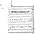
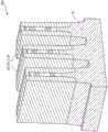
图1根据一些实施例方案示出在半导体制造过程期间的半导体器件100的一部分的示意视图。在图1实例中,Si/SiGe鳍蚀刻已经完成,并且衬垫氧化物/SiN盖层留在鳍的顶部上。在这个特定情况下,鳍蚀刻已经在鳍蚀刻过程之前进行。这意味着在STI下面的硅被认为在鳍之间的区域中是“平坦”的。利用鳍最后切割方法,在这个步骤之前蚀刻虚设鳍,如此在鳍之间的硅内提供深凹陷,这使形成埋入式电力轨道更加困难。因此,对于将埋入式电力轨道合并到这个实例集成中,合并用于鳍式图案定义的鳍先切割或鳍中间切割方法是优选的。以下图式示出示例结果。FIG. 1 shows a schematic view of a portion of a
图2示出在通过沉积氧化物和CMP回到Si/SiGe鳍式结构的顶部进行浅沟槽隔离(STI)之后的半导体器件100的示意视图。2 shows a schematic view of
图3示出在光刻胶层中产生用于轨道沟槽的图案之后的半导体器件100的示意视图。在图3实例中,将多层光刻堆叠用于图案转移。所述多层光刻堆叠包括旋涂碳(SOC)的底部层、含硅抗反射涂层(SiARC)的中间层和顶部层光刻胶。在一实例中,首先将光刻胶中的图案转移到中间层SiARC和底部层SOC。然后,例如通过轨道沟槽蚀刻将中间层SiARC和底部层SOC中的图案向下转移到STI氧化物。FIG. 3 shows a schematic view of the
图4示出在埋入式轨道沟槽蚀刻之后的半导体器件100的示意视图。请注意,在STI氧化物的顶部上图案化埋入式轨道沟槽,并且例如通过蚀刻穿过STI氧化物转移埋入式轨道沟槽。在一实例中,图案转移在STI氧化物的深度内完全停止。在另一实例中,图案转移完全穿过STI氧化物的深度并且延伸到块状硅中来蚀刻。对于宽(与布线线相比,1.5T到4T宽的轨道)电力轨道的情况,这个沟槽的高宽比为大约2.5到5.0。深且窄的轨道能够具有至多3倍的高宽比,或7.5到15.0。这个蚀刻过程将产生极薄(<12nm)的STI氧化物,所述STI氧化物能够深达埋入式电力轨道在STI内的期望深度。在鳍之间的氧化物填充物内转移这些窄沟槽的挑战包括埋入式电力轨道之间的间隔的倒塌余度和失真。以下图式示出示例结果。FIG. 4 shows a schematic view of the
在FINFET应用中,块状硅能够是重掺杂的,并且将轨道完全保持在STI内是优选的。然而,在STI内保持深轨道使鳍的初始高度比常规制造的鳍大得多。典型地,对于FINFET,鳍尺寸围绕75A延伸,因此在这个示例实施方案中,鳍的高宽比能够扩大超过15-1并且甚至接近20-1。由于这是极其攻击性的并且倾向于导致鳍形状的失真,因此对于一些实施方案,优选的是将埋入式轨道赶到硅中。在一个实施方案中,能够通过自对准过程来形成窄的埋入式轨道,其中初始沟槽是更一般的1.5T到4T电力轨道的大小,尽管初始沟槽是穿过STI蚀刻。In FINFET applications, the bulk silicon can be heavily doped, and keeping the tracks completely within the STI is preferred. However, maintaining deep orbits within the STI allows the initial height of the fins to be much larger than conventionally fabricated fins. Typically, for FINFETs, the fin size extends around 75A, so in this example embodiment, the aspect ratio of the fin can expand beyond 15-1 and even approach 20-1. Since this is extremely aggressive and tends to distort the fin shape, for some embodiments it is preferable to drive the buried track into the silicon. In one embodiment, narrow buried tracks can be formed by a self-alignment process, where the initial trenches are the size of a more typical 1.5T to 4T power track, although the initial trenches are etched through STI.
在埋入式轨道沟槽向下延伸到块状硅的实施方案中,埋入式轨道获益于通过在图案转移到块状硅中之后将介电质共形沉积到沟槽中而与块状硅物理上隔离。In embodiments in which the buried track trenches extend down into the bulk silicon, the buried tracks benefit from a The silicon is physically isolated.
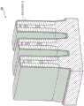
图5示出在沉积线性、例如原子层沉积(ALD)SiO衬里之后的半导体器件100的示意视图。5 shows a schematic view of a
在达到埋入式电力轨道的期望深度后,能够在沟槽内共形地沉积蚀刻选择性薄膜以在沟槽的两侧上形成“隔离物”。这种蚀刻选择性材料接着能够经受一般“隔离物打开”蚀刻以去除沟槽的底部处的共形沉积,从而仅留下沿着宽沟槽的侧壁的蚀刻选择性材料。After reaching the desired depth of the buried power track, an etch selective film can be conformally deposited within the trench to form "spacers" on both sides of the trench. This etch-selective material can then be subjected to a general "spacer-on" etch to remove the conformal deposition at the bottom of the trench, leaving only the etch-selective material along the sidewalls of the wide trench.
在本文中的一个实施方案中,也能够通过自对准过程形成窄的埋入式轨道,其中初始沟槽具有更一般的1.5T到4T电力轨道的大小,尽管初始沟槽是穿过STI蚀刻。在达到埋入式电力轨道的期望深度后,能够在沟槽内共形地沉积蚀刻选择性薄膜以在沟槽的两侧上形成“隔离物”。In one embodiment herein, it is also possible to form narrow buried tracks by a self-aligned process, where the initial trenches have the size of a more typical 1.5T to 4T power track, although the initial trenches are etched through STI . After reaching the desired depth of the buried power track, an etch selective film can be conformally deposited within the trench to form "spacers" on both sides of the trench.
图6示出在沉积蚀刻选择性薄膜(例如,ALD牺牲膜)之后的半导体器件100的示意视图。6 shows a schematic view of the
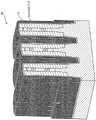
这种蚀刻选择性材料接着能够经受一般“隔离物开口”蚀刻以去除沟槽的底部处的共形沉积,从而仅留下沿着宽沟槽的侧壁的蚀刻选择性材料。接着使用氧化物或其他介电衬里和/或填充材料以填充沟槽的剩余部分,然后对氧化物或其他介电衬里和/或填充材料进行平面化(例如CMP)或进行向下的干式或湿式凹陷以暴露“A/B”基质,其中A是STI氧化物或填充氧化物,而B是沟槽内的蚀刻选择性材料。This etch selective material can then be subjected to a general "spacer opening" etch to remove the conformal deposition at the bottom of the trench, leaving only the etch selective material along the sidewalls of the wide trench. An oxide or other dielectric liner and/or fill material is then used to fill the remainder of the trench, and the oxide or other dielectric liner and/or fill material is then planarized (eg, CMP) or dry down Or wet recessed to expose the "A/B" matrix, where A is the STI oxide or fill oxide and B is the etch selective material within the trench.
图7示出在氧化物填充之后的半导体器件100的示意视图。FIG. 7 shows a schematic view of the
此外,接着能够使用非攻击性蚀刻过程以挖出蚀刻选择性材料“B”,这将导致形成两个相同的沟槽。Furthermore, a non-aggressive etch process can then be used to dig out the etch selective material "B", which will result in the formation of two identical trenches.
图8示出在形成两个相同沟槽之后的半导体器件100的示意视图。FIG. 8 shows a schematic view of the
在一实施方案中,所述两个沟槽能够相同,这是因为所述两个沟槽最初是通过单一的共形沉积过程形成。存在放置两个邻近窄沟槽之间的氧化物塌陷的多种低攻击性蚀刻过程。一个此种过程是能够达成至多百分之一的选择性的化学氧化物去除(COR)气相蚀刻,以及其他准原子层蚀刻(ALE)和湿式和或干式蚀刻。以下图式示出示例结果。In one embodiment, the two trenches can be identical because the two trenches are initially formed by a single conformal deposition process. There are various low-aggressive etch processes that place oxide collapses between two adjacent narrow trenches. One such process is Chemical Oxide Removal (COR) vapor phase etching capable of achieving selectivity of up to one percent, as well as other quasi-atomic layer etching (ALE) and wet and or dry etching. The following graphs show example results.
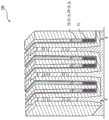
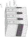
接下来,在一实例中,用将用于埋入式电力轨道的金属和/或衬里填充沟槽的底部。对用于埋入式电力轨道的金属化的选择是基于在集成流程中的什么位置形成轨道并且对轨道进行金属化。对于恰好在进行S/D外延的尖端退火之前形成并且金属化埋入式轨道的情况,金属必须具有极好的在氧化物上的热特性-确切地说,金属能够在介于700C与1100C之间的尖端退火温度以及用于金属栅极中的薄膜的沉积温度下稳定。对于埋入式轨道是在金属栅极沉积和S/D尖端退火之前放置的实施方案,这将排除例如铜(<450C热稳定性)、钴或铝的金属的使用。然而,可选择钌以用于在集成中的这一点处将埋入式电力轨道金属化,条件是钌与氧化物相比具有极好的热稳定性,并且也能够使用自底向上沉积过程将钌沉积到深沟槽中。然而,如果使用例如钌的金属;由于钌的电阻率及其随后电阻,这将使埋入式电力轨道变成窄轨道而不是1.5T到4T大小的轨道。由于自底向上形成到窄电力轨道的连接可能更困难,因此在一些实施方案中,到金属漏极的连接能够自对准。以下图式示出示例结果。Next, in one example, the bottom of the trench is filled with the metal and/or liner that will be used for the buried power rail. The choice of metallization for buried power rails is based on where in the integration flow the rails are formed and metallized. For buried tracks to be formed and metallized just before tip annealing for S/D epitaxy, the metal must have excellent thermal properties on the oxide - to be precise, the metal can operate between 700C and 1100C Stable between tip annealing temperatures and deposition temperatures for thin films in metal gates. For embodiments where the buried track is placed prior to metal gate deposition and S/D tip annealing, this would preclude the use of metals such as copper (<450C thermal stability), cobalt or aluminum. However, ruthenium can be selected for metallization of the buried power rails at this point in the integration, provided that ruthenium has excellent thermal stability compared to oxides and can also be deposited using a bottom-up deposition process. Ruthenium is deposited into deep trenches. However, if a metal such as ruthenium is used; this will make the buried power track a narrow track instead of a 1.5T to 4T sized track due to the resistivity of ruthenium and its subsequent resistance. Since bottom-up connections to narrow power rails can be more difficult, in some implementations, connections to metal drains can be self-aligned. The following graphs show example results.
图9示出在用钌填充沟槽的底部之后的半导体器件100的示意视图。在一实例中,在沟槽和表面上方填充钌,并且将钌回蚀(凹陷)到沟槽的底部。FIG. 9 shows a schematic view of the
本文中的技术包括通过在凹陷钌(或任何其他金属)上方使用蚀刻选择性盖层而将电力轨道自底向上自对准到金属漏极。请注意,当通过替换方法形成电力轨道时,金属化能够在S/D尖端退火之后或在实际金属漏极金属化期间执行。对于钌的情况,盖层可以是(a)介电质并且具有足够大小以成为电力轨道与位于轨道上方的金属漏极之间的真正介电质,或(b)或对边界STI氧化物或介电衬里具有蚀刻选择性。The techniques herein include bottom-up self-alignment of power rails to metal drains by using an etch selective cap layer over recessed ruthenium (or any other metal). Note that when the power rails are formed by alternative methods, the metallization can be performed after the S/D tip anneal or during the actual metal drain metallization. In the case of ruthenium, the capping layer can be either (a) a dielectric and of sufficient size to be the true dielectric between the power track and the metal drain above the track, or (b) either a boundary STI oxide or The dielectric liner has etch selectivity.
图10示出在凹陷的钌上方形成蚀刻选择性盖层之后的半导体器件100的示意视图。10 shows a schematic view of a
接着用STI氧化物或其他介电质填充埋入式轨道沟槽的剩余部分,接着向下抛光到鳍式结构的顶部。The remainder of the buried track trench is then filled with STI oxide or other dielectric, and then polished down to the top of the fin structure.
图11示出在填充STI氧化物并且进行向下抛光之后的半导体器件100的示意视图。FIG. 11 shows a schematic view of the
接下来,能够执行STI凹陷蚀刻过程以使STI下降到有效鳍的顶部或下降到用于互补式堆叠式纳米片的这个实例的SiGe。STI蚀刻能够在埋入式电力轨道上方在蚀刻选择性介电质盖层的顶部处停止。Next, an STI recess etch process can be performed to bring the STI down to the top of the active fin or down to SiGe for this example of the complementary stacked nanosheet. The STI etch can be stopped at the top of the etch selective dielectric cap above the buried power rails.
图12示出在STI凹陷蚀刻过程之后的半导体器件100的示意视图。FIG. 12 shows a schematic view of the
请注意,能够使用其他任选实施方案将埋入式电力轨道金属化,以达到除钌外的金属选择或其他可选择性沉积的金属。使其他金属能够并入到埋入式电力轨道中的另一选项是形成完全替换金属轨道,其中在埋入式轨道沟槽限定过程期间,替代用金属填充轨道并且用蚀刻选择性介电质封盖,用介电质完全填充沟槽,然后将沟槽向下凹陷到金属化的埋入式轨道的期望高度。在到金属漏极的后续连接期间,能够各向同性地去除整个替换轨道,然后用金属进行重新填充。埋入式电力轨道非分散地在给定单元上延伸并且达到邻近的给定单元是有益的。具有这种连续的电力轨道金属可以是挑战。在这种实施方案中,从到金属漏极的有效接触点以及不需要连接的点去除整个替换轨道。当填充金属时,这种情况下的填充将执行为“地下”填充(而不是简单的自上而下或自底向上填充),其中金属沿着在金属漏极下延伸的埋入式轨道的长度延伸,不需要到轨道的连接。Note that buried power rails can be metallized using other optional embodiments to achieve metal options other than ruthenium or other selectively depositable metals. Another option to enable the incorporation of other metals into the buried power rails is to form full replacement metal rails, where the rails are instead filled with metal and sealed with an etch selective dielectric during the buried rail trench definition process. cover, completely fill the trench with dielectric, and then recess the trench down to the desired height of the metallized buried track. During subsequent connections to the metal drain, the entire replacement track can be removed isotropically and then refilled with metal. It is beneficial for buried power rails to extend non-distributedly over a given cell and reach adjacent given cells. Having such a continuous power track metal can be challenging. In such an embodiment, the entire replacement track is removed from the active contact point to the metal drain and the point where no connection is required. When filling metal, the filling in this case will be performed as an "underground" filling (rather than a simple top-down or bottom-up filling), where the metal follows the direction of the buried track extending under the metal drain The length is extended and no connection to the track is required.
继续本文中的集成实施方案,其中轨道恰被金属化并且用蚀刻选择性介电质盖层封盖,过程流程继续到在S/D已经通过尖端退火和以后的替换金属栅极金属化形成之后。在集成流程中的这一点,实现期望金属漏极与到电力轨道的选定接触点之间的接触。Continuing with the integrated embodiment herein, where the tracks are just metallized and capped with an etch selective dielectric cap layer, the process flow continues after the S/D has been formed by tip annealing and subsequent replacement metal gate metallization . At this point in the integration flow, the contact between the desired metal drain and the selected contact point to the power rail is achieved.
示例性实施方案使用互补式FET堆叠式纳米片作为实例,描述主要关注从金属漏极到Vss的分接头,所述分接头连接到两个堆叠式电极的大部分底部(底部为NMOS并且顶部为PMOS)。Using complementary FET stacked nanosheets as an example, the description focuses on the tap from the metal drain to Vss that connects to most of the bottom of the two stacked electrodes (NMOS on the bottom and NMOS on the top). PMOS).
此时,金属漏极还没有被金属化,并且在金属栅极的金属化期间用氧化物填充金属漏极。此时,金属漏极内的氧化物向下凹陷到在埋入式电力轨道上方的蚀刻选择性介电质盖层的顶部(或氧化物能够全部去除,如果STI与金属漏极填充氧化物之间存在蚀刻止挡件)。并入盖层的蚀刻选择性性质确保当打开金属漏极时,能够使用自对准的蚀刻过程,其中盖层能够在不另外打开沿着埋入式轨道的轴线的STI氧化物的情况下被打开。这也使得整个金属漏极能够将盖层打开到埋入式电力轨道,并且始终控制分接头具有与初始埋入式轨道沟槽的大小相同的大小,所述大小也等于埋入式电力轨道本身的大小减去沟槽内的另外沉积的衬里的大小。这允许完全自由地使用金属漏极的大小,这对接脚访问有限的面积级器件有益。At this point, the metal drain has not been metallized, and the metal drain is filled with oxide during the metallization of the metal gate. At this point, the oxide in the metal drain is recessed down to the top of the etch selective dielectric cap layer over the buried power rails (or the oxide can be completely removed, if the STI is between the metal drain fill oxide There is an etch stop in between). The etch selectivity nature of the incorporated capping layer ensures that a self-aligned etch process can be used when opening the metal drain, wherein the capping layer can be removed without additionally opening the STI oxide along the axis of the buried track. Open. This also enables the entire metal drain to open the cap layer to the buried power rail and always control the tap to have the same size as the initial buried rail trench, which is also equal to the buried power rail itself minus the size of the additional deposited liner within the trench. This allows complete freedom to use the size of the metal drain, which is beneficial for area-level devices with limited pin access.
图13示出在将金属漏极内的氧化物向下凹陷到蚀刻选择性介电质盖层的顶部之后的半导体器件100的示意视图。13 shows a schematic view of the
能够用氧化物(如果氧化物与STI之间存在止挡层)或用通常被称为替换触点的某一其他材料来填充金属漏极。替换触点一般具有对多个薄膜的极好选择性:(a)STI中的氧化物;(b)保护埋入式轨道的介电质盖层;(c)保护金属栅极的盖层,其通常是某一类型的氮化物;和(d)低k栅极隔离物。以下图式示出示例结果。The metal drain can be filled with oxide (if there is a stop layer between oxide and STI) or with some other material commonly referred to as a replacement contact. Replacement contacts generally have excellent selectivity to multiple films: (a) oxide in STI; (b) dielectric cap protecting buried track; (c) cap protecting metal gate, It is usually some type of nitride; and (d) a low-k gate spacer. The following graphs show example results.
图14示出在用替换触点填充之后的半导体器件100的示意视图。FIG. 14 shows a schematic view of the
到电力轨道的电力分接头被成像(图案化)并且穿过替换触点向下转移。由于埋入式电力轨道会使BEOL金属线成为一系列致密的布线线,因此南北定向上的单元之间的间隔将仅为1/2临界金属间距,或出于铸造N5技术的考虑,大致为12nm。对于沿着电力轨道纵向轴线的到同一位置的由两个邻近单元形成的电力分接头,这意味着将难以对离散通孔成像,即使是利用EUV多图案化。因此自对准是有益的,以便确保这种情形不造成邻近单元之间的短接。这是自对准是因为初始的宽沟槽经过自对准图案化以形成两个相同的窄轨道的情况。因此,每一“对”轨道将与Vdd或Vss对应,这是因为南北定向上的单元共享Vss或Vdd轨道,这种自对准方法不仅提供电阻改进,而且确定两个邻近单元不短接。The power taps to the power rails are imaged (patterned) and transferred down through the replacement contacts. Since the buried power rails would make the BEOL wire a series of dense wiring, the spacing between cells in a north-south orientation would be only 1/2 the critical metal spacing, or roughly for cast N5 technology considerations 12nm. For a power tap formed by two adjacent cells to the same location along the longitudinal axis of the power rail, this means that it will be difficult to image discrete vias, even with EUV multi-patterning. Self-alignment is therefore beneficial in order to ensure that this situation does not create shorts between adjacent cells. This is the case for self-alignment because the initial wide trenches are self-aligned patterned to form two identical narrow tracks. Thus, each "pair" of tracks will correspond to Vdd or Vss, since cells in a north-south orientation share the Vss or Vdd track, this self-alignment approach not only provides resistance improvement, but also ensures that two adjacent cells are not shorted.
图15示出在将电力分接头在例如来自光刻胶层的SiARC层和SOC层中成像之后的半导体器件100的示意视图。15 shows a schematic view of the
在需要到电力轨道的分接的情况下,能够去除电力轨道上方的蚀刻选择性盖层以实现金属漏极触点。In the event that a tap to the power rail is required, the etch selective cap layer over the power rail can be removed to achieve a metal drain contact.
图16示出在去除蚀刻选择性盖层之后的半导体器件100的示意视图。FIG. 16 shows a schematic view of the
接着能够去除金属漏极中的替换触点材料。The replacement contact material in the metal drain can then be removed.
图17示出在去除替换触点之后的半导体器件100的示意视图。FIG. 17 shows a schematic view of the
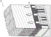
接着可对金属漏极进行金属化,其中到所要轨道的连接被相等地填充,而不需要的连接仍被蚀刻选择性盖层堵塞,所述蚀刻选择性盖层在穿过金属漏极转移分接头期间不打开。The metal drain can then be metallized, with connections to the desired tracks being equally filled, while the unwanted connections remain blocked by an etch-selective cap layer that transfers the separation through the metal drain. Do not open during splice.
图18示出在底部电极的漏极金属化之后的半导体器件100的示意视图。Figure 18 shows a schematic view of the
对于互补式堆叠式纳米片FET的情况,需要将底部电极(NMOS)与上部电极(PMOS)分开进行金属化。同样地,到Vss轨道和Vdd轨道的电力分接头针对两组电极出现。在本文中的实施方案中,可使用多个金属化和蚀刻步骤或经由选择性沉积来执行单独的金属化。In the case of complementary stacked nanosheet FETs, the bottom electrode (NMOS) needs to be metallized separately from the top electrode (PMOS). Likewise, power taps to the Vss rail and the Vdd rail occur for both sets of electrodes. In embodiments herein, a single metallization may be performed using multiple metallization and etch steps or via selective deposition.
图19示出在图案化底部电极的金属化和沉积氧化物层之后的半导体器件100的示意视图。19 shows a schematic view of the
图20示出在顶部电极的漏极金属化和沉积氧化物层之后的半导体器件100的示意视图。20 shows a schematic view of the
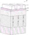
请注意,在半导体器件100中,每个电力轨道包括两个使用开放式隔离物技术形成的轨道线。可修改所述过程以形成例如图21到图30所示的宽电力轨道。Note that in
图21根据一些实施方案示出在半导体制造过程期间的半导体器件200的一部分的示意视图。图21类似于图1。在图21实例中,Si/SiGe鳍蚀刻已经完成,并且衬垫氧化物/SiN盖层留在鳍的顶部上。21 shows a schematic view of a portion of a
图22示出在通过沉积氧化物并且CMP回到Si/SiGe鳍式结构的顶部进行浅沟槽隔离(STI)之后的半导体器件200的示意视图。图22类似于图2。22 shows a schematic view of a
图23示出在光刻胶层中产生用于轨道沟槽的图案之后的半导体器件200的示意视图。图23类似于图3。23 shows a schematic view of a
图24示出当例如通过蚀刻来穿过STI氧化物转移图案时的半导体器件200的示意视图。24 shows a schematic view of a
图25示出当将图案另外转移到块状硅中时的半导体器件200的示意视图。在一实例中,在图案转移到硅中之前沉积隔离物层以帮助到硅中的图案转移。FIG. 25 shows a schematic view of a
图26示出在沉积例如SiO/TaN衬里的蚀刻选择薄膜之后的半导体器件200的示意视图。FIG. 26 shows a schematic view of a
图27示出在钌底部填充之后的半导体器件200的示意视图。FIG. 27 shows a schematic view of a
图28示出在回蚀钌之后的半导体器件200的示意视图。钌在轨道沟槽中蚀刻凹陷到特定深度。此外,去除衬里中的TaN。FIG. 28 shows a schematic view of a
图29示出在凹陷的钌上方形成蚀刻选择性盖层之后的半导体器件200的示意视图。29 shows a schematic view of a
图30示出在对STI氧化物进行填充和向下抛光之后的半导体器件200的示意视图。30 shows a schematic view of a
此外,参考图12到图20所描述的类似过程能够用于继续关于半导体器件200的制造过程。Furthermore, similar processes described with reference to FIGS. 12-20 can be used to continue the fabrication process with respect to the
请注意,半导体器件100和200是具有堆叠式器件的3D器件。用于制造埋入式电力轨道的操作能够整合以实现不堆叠的规则FINFET。图31到图39根据公开的一些实施方案示出用于形成FINFET器件的埋入式电力轨道的中间阶段的各种示意视图。Note that the
图31根据一些实施方案示出在半导体制造过程期间的半导体器件300的一部分的示意视图。在图31实例中,Si鳍蚀刻已经完成,并且衬垫氧化物/SiN盖层留在鳍的顶部上。31 shows a schematic view of a portion of a
图32示出在通过沉积氧化物并且CMP回到Si/SiGe鳍式结构的顶部进行浅沟槽隔离(STI)之后的半导体器件300的示意视图。32 shows a schematic view of a
图33示出当例如通过蚀刻穿过STI氧化物转移图案时的半导体器件300的示意视图。33 shows a schematic view of a
图34示出在沉积隔离物层之后的半导体300的示意视图。隔离物层能够通过以下操作帮助到硅中的图案转移:(a)确保任何打开的硅或SiGe鳍式结构在将埋入式轨道沟槽图案转移到块状硅中期间不被蚀刻;和(b)经由原子层沉积确保最后的埋入式电力轨道与硅、SiGe或硅/SiGe鳍式结构之间存在固定并且可控的距离。FIG. 34 shows a schematic view of
图35示出当将图案另外转移到块状硅中时的半导体器件300的示意视图。35 shows a schematic view of a
图36示出当沉积例如SiO/TaN衬里的蚀刻选择性薄膜,然后从沟槽的底部填充钌时的的半导体器件300的示意视图。36 shows a schematic view of a
图37示出在对钌回蚀之后的半导体器件300的示意视图。钌在轨道沟槽中蚀刻凹陷到特定深度。此外,去除衬里中的TaN。FIG. 37 shows a schematic view of a
图38示出在凹陷的钌上方形成蚀刻选择性盖层之后的半导体器件300的示意视图。38 shows a schematic view of a
图39示出在晶片制造过程之后的半导体器件300的示意视图。FIG. 39 shows a schematic view of a
如上所述,本文中的示例实施方案关注埋入式电力轨道的应用。这只是一个示例实施方案,能够扩展本文中的技术以覆盖任何背面接线,例如存在于物理设备或晶体管器件下面的布线线或局部互连或单元到单元互连线。As mentioned above, example embodiments herein focus on the application of buried power rails. This is just one example embodiment, and the techniques herein can be extended to cover any backside wiring, such as wiring lines or local interconnects or cell-to-cell interconnects that exist under a physical device or transistor device.
在先前描述中,已经描述特定细节,例如处理系统的特定几何形状和对本文中所使用的各种部件和过程的描述。然而,应了解,可以在背离这些特定细节的其他实施方案中实践本文中的技术,并且这些细节用于解释目的,而不是限制。已经参考附图描述本文中公开的实施方案。类似地,出于解释目的,已经陈述特定的数字、材料和配置,以便提供透彻理解。尽管如此,可以在不具有这些特定细节的情况下实践实施方案。具有基本上相同的功能构造的部件是由类似的参考字符表示,并且因此可以省略任何冗余的描述。In the previous description, specific details have been described, such as the specific geometry of the processing system and descriptions of various components and processes used herein. It is to be understood, however, that the techniques herein may be practiced in other embodiments that depart from these specific details, and these details are for purposes of explanation and not limitation. The embodiments disclosed herein have been described with reference to the accompanying drawings. Similarly, for purposes of explanation, specific numbers, materials and configurations have been set forth in order to provide a thorough understanding. Nonetheless, embodiments may be practiced without these specific details. Components having substantially the same functional configuration are denoted by similar reference characters, and thus any redundant description may be omitted.
已将各种技术描述为多个离散操作以帮助理解各种实施方案。描述的次序不应解释为暗示这些操作必须取决于次序。实际上,这些操作不必按呈现的次序执行。可以用不同于所描述实施方案的次序执行所描述的操作。在额外实施方案中,可以执行各种额外操作和/或可以省略所描述操作。Various techniques have been described as multiple discrete operations to assist in understanding the various embodiments. The order of description should not be construed to imply that these operations are necessarily order dependent. In fact, these operations do not have to be performed in the order presented. Operations described may be performed in an order different from that of the described embodiments. In additional embodiments, various additional operations may be performed and/or described operations may be omitted.
如本文中所使用的“衬底”或“目标衬底”通常是指根据本发明加以处理的物件。衬底可以包括器件、特别是半导体器件或其他电子器件的任何材料部分或结构,并且可以是例如基底衬底结构,例如半导体晶片、光罩或在例如薄膜的基底衬底结构上或上覆的层。因此,衬底不限于经图案化或未图案化的任何特定的基底结构、下伏层或上覆层,而是预期包括任何此层或基底结构,和层和/或基底结构的任何组合。描述可以参考特定类型的衬底,但是这仅用于说明目的。A "substrate" or "target substrate" as used herein generally refers to an item that is processed in accordance with the present invention. The substrate may comprise any material portion or structure of a device, particularly a semiconductor device or other electronic device, and may be, for example, a base substrate structure such as a semiconductor wafer, a photomask, or on or overlying a base substrate structure such as a thin film Floor. Thus, the substrate is not limited to any particular base structure, underlying layer, or overlying layer, patterned or unpatterned, but is intended to include any such layer or base structure, and any combination of layers and/or base structures. The description may refer to a particular type of substrate, but this is for illustration purposes only.
本领域的技术人员还将理解,能够对上文解释的技术的操作作出许多改变,同时仍实行本发明的相同目标。这些改变意图被本公开的范围覆盖。因而,本发明的实施方案的先前描述并不意图是限制性的。实际上,在权利要求中提出对本发明的实施方案的任何限制。Those skilled in the art will also appreciate that many changes can be made to the operation of the techniques explained above while still carrying out the same objectives of the present invention. These changes are intended to be covered by the scope of this disclosure. Thus, the foregoing description of embodiments of the present invention is not intended to be limiting. Indeed, any limitations to embodiments of the invention are set forth in the claims.
Claims (22)
Applications Claiming Priority (3)
| Application Number | Priority Date | Filing Date | Title |
|---|---|---|---|
| US201762523704P | 2017-06-22 | 2017-06-22 | |
| US62/523,704 | 2017-06-22 | ||
| PCT/US2018/038678WO2018237106A1 (en) | 2017-06-22 | 2018-06-21 | FEEDING RAILS |
Publications (2)
| Publication Number | Publication Date |
|---|---|
| CN110800113Atrue CN110800113A (en) | 2020-02-14 |
| CN110800113B CN110800113B (en) | 2023-06-06 |
Family
ID=64692751
Family Applications (1)
| Application Number | Title | Priority Date | Filing Date |
|---|---|---|---|
| CN201880041590.9AActiveCN110800113B (en) | 2017-06-22 | 2018-06-21 | Buried Power Track |
Country Status (6)
| Country | Link |
|---|---|
| US (1) | US10586765B2 (en) |
| JP (1) | JP6865864B2 (en) |
| KR (1) | KR102380098B1 (en) |
| CN (1) | CN110800113B (en) |
| TW (1) | TWI734919B (en) |
| WO (1) | WO2018237106A1 (en) |
Cited By (4)
| Publication number | Priority date | Publication date | Assignee | Title |
|---|---|---|---|---|
| CN113206080A (en)* | 2020-04-30 | 2021-08-03 | 台湾积体电路制造股份有限公司 | Integrated circuit and forming method thereof |
| CN113299648A (en)* | 2020-06-05 | 2021-08-24 | 台湾积体电路制造股份有限公司 | Semiconductor device and method for manufacturing the same |
| WO2023029746A1 (en)* | 2021-09-01 | 2023-03-09 | International Business Machines Corporation | Complementary fet (cfet) buried sidewall contact with spacer foot |
| TWI818638B (en)* | 2021-11-16 | 2023-10-11 | 美商萬國商業機器公司 | Replacement buried power rail |
Families Citing this family (93)
| Publication number | Priority date | Publication date | Assignee | Title |
|---|---|---|---|---|
| US10700207B2 (en)* | 2017-11-30 | 2020-06-30 | Taiwan Semiconductor Manufacturing Company Ltd. | Semiconductor device integrating backside power grid and related integrated circuit and fabrication method |
| DE102018127448B4 (en) | 2017-11-30 | 2023-06-22 | Taiwan Semiconductor Manufacturing Co. Ltd. | Metal busbar for non-planar semiconductor devices |
| US10672665B2 (en)* | 2018-09-28 | 2020-06-02 | Taiwan Semiconductor Manufacturing Co., Ltd. | Fin field effect transistor device structure and method for forming the same |
| US11527640B2 (en) | 2019-01-03 | 2022-12-13 | Intel Corporation | Wrap-around contact structures for semiconductor nanowires and nanoribbons |
| US12354991B2 (en) | 2019-02-19 | 2025-07-08 | Tokyo Electron Limited | Replacement buried power rail in backside power delivery |
| US10985103B2 (en) | 2019-03-01 | 2021-04-20 | Samsung Electronics Co., Ltd | Apparatus and method of forming backside buried conductor in integrated circuit |
| KR102798340B1 (en) | 2019-05-16 | 2025-04-23 | 삼성전자주식회사 | Semiconductor device |
| KR102760926B1 (en)* | 2019-05-20 | 2025-02-03 | 삼성전자주식회사 | Integrated circuit device and method of manufacturing the same |
| US11195797B2 (en) | 2019-05-21 | 2021-12-07 | Samsung Electronics Co., Ltd. | Applications of buried power rails |
| KR102801648B1 (en)* | 2019-05-21 | 2025-05-02 | 삼성전자주식회사 | Semiconductor device |
| US10886224B2 (en) | 2019-05-22 | 2021-01-05 | Samsung Electronics Co., Ltd. | Power distribution network using buried power rail |
| KR102712328B1 (en) | 2019-05-22 | 2024-09-30 | 삼성전자주식회사 | Semiconductor device |
| WO2020235084A1 (en) | 2019-05-23 | 2020-11-26 | 株式会社ソシオネクスト | Semiconductor device |
| WO2020235082A1 (en) | 2019-05-23 | 2020-11-26 | 株式会社ソシオネクスト | Semiconductor device |
| US11335599B2 (en)* | 2019-05-24 | 2022-05-17 | Tokyo Electron Limited | Self-aligned contacts for 3D logic and memory |
| US11233008B2 (en) | 2019-06-19 | 2022-01-25 | Samsung Electronics Co., Ltd. | Method of manufacturing an integrated circuit with buried power rail |
| US11101217B2 (en) | 2019-06-27 | 2021-08-24 | International Business Machines Corporation | Buried power rail for transistor devices |
| EP3770952B1 (en)* | 2019-07-24 | 2025-05-14 | Imec VZW | Method for forming a buried metal line in a semiconductor substrate |
| US11735525B2 (en) | 2019-10-21 | 2023-08-22 | Tokyo Electron Limited | Power delivery network for CFET with buried power rails |
| US12057322B2 (en) | 2019-10-21 | 2024-08-06 | Tokyo Electron Limited | Methods for etching metal films using plasma processing |
| CN112701082B (en)* | 2019-10-23 | 2024-12-20 | 中芯国际集成电路制造(上海)有限公司 | Semiconductor structure and method for forming the same |
| US11309240B2 (en) | 2019-10-31 | 2022-04-19 | Taiwan Semiconductor Manufacturing Co., Ltd. | Conductive rail structure for semiconductor devices |
| EP3836196B1 (en)* | 2019-12-13 | 2023-04-26 | Imec VZW | Self-aligned contacts for nanosheet field effect transistor devices |
| EP3840054B1 (en) | 2019-12-20 | 2023-07-05 | Imec VZW | Self-aligned contacts for walled nanosheet and forksheet field effect transistor devices |
| DE102020125647A1 (en)* | 2020-01-31 | 2021-08-05 | Taiwan Semiconductor Manufacturing Co., Ltd. | Complementary field effect transistor semiconductor device of buried logic conductor type, layout diagram manufacturing method and system therefor |
| US11362090B2 (en)* | 2020-01-31 | 2022-06-14 | Taiwan Semiconductor Manufacturing Company, Ltd. | Semiconductor device having buried logic conductor type of complementary field effect transistor, method of generating layout diagram and system for same |
| US11195794B2 (en) | 2020-02-05 | 2021-12-07 | Samsung Electronics Co., Ltd. | Stacked integrated circuit devices including a routing wire |
| US11217533B2 (en) | 2020-02-07 | 2022-01-04 | Globalfoundries U.S. Inc. | Semiconductor device with metal structure under an active layer |
| US11145550B2 (en) | 2020-03-05 | 2021-10-12 | International Business Machines Corporation | Dummy fin template to form a self-aligned metal contact for output of vertical transport field effect transistor |
| US11217528B2 (en) | 2020-04-01 | 2022-01-04 | Taiwan Semiconductor Manufacturing Company, Ltd. | Semiconductor structure having buried power rail disposed between two fins and method of making the same |
| US11342413B2 (en)* | 2020-04-24 | 2022-05-24 | Taiwan Semiconductor Manufacturing Co., Ltd. | Selective liner on backside via and method thereof |
| DE102021102235A1 (en)* | 2020-04-29 | 2021-11-04 | Taiwan Semiconductor Manufacturing Co., Ltd. | INTEGRATED CIRCUIT WITH REAR CONTACT |
| US11676896B2 (en)* | 2020-04-30 | 2023-06-13 | Taiwan Semiconductor Manufacturing Company, Ltd. | Integrated circuit and method for forming the same |
| DE102021103469B4 (en) | 2020-04-30 | 2024-09-26 | Taiwan Semiconductor Manufacturing Co., Ltd. | INTEGRATED CIRCUIT AND METHOD FOR MANUFACTURING THE SAME |
| DE102020132602B4 (en) | 2020-05-13 | 2023-06-29 | Taiwan Semiconductor Manufacturing Co., Ltd. | SEMICONDUCTOR DEVICE WITH BURIED CONDUCTIVE FINGERS AND ITS METHOD OF MANUFACTURE |
| US12027461B2 (en)* | 2020-05-13 | 2024-07-02 | Taiwan Semiconductor Manufacturing Company, Ltd. | Semiconductor device including buried conductive fingers and method of making the same |
| KR20210138995A (en) | 2020-05-13 | 2021-11-22 | 삼성전자주식회사 | Integrated circuit including standard cells, and method for fabricating the same |
| WO2021229740A1 (en)* | 2020-05-14 | 2021-11-18 | 株式会社ソシオネクスト | Semiconductor device and method for manufacturing same |
| DE102021106180A1 (en)* | 2020-05-14 | 2021-11-18 | Taiwan Semiconductor Manufacturing Co., Ltd. | INTEGRATED CIRCUIT, SYSTEM, AND PROCESS FOR ITS MANUFACTURING |
| US11569168B2 (en) | 2020-05-14 | 2023-01-31 | Taiwan Semiconductor Manufacturing Company, Ltd. | Integrated circuit, system and method of forming the same |
| US11257758B2 (en)* | 2020-06-24 | 2022-02-22 | Taiwan Semiconductor Manufacturing Company Limited | Backside connection structures for nanostructures and methods of forming the same |
| WO2021259479A1 (en)* | 2020-06-25 | 2021-12-30 | Huawei Technologies Co., Ltd. | Semiconductor device, semiconductor die, and method of manufacturing a semiconductor device |
| US11569246B2 (en) | 2020-06-29 | 2023-01-31 | Taiwan Semiconductor Manufacturing Company, Ltd. | Four CPP wide memory cell with buried power grid, and method of fabricating same |
| US11393819B2 (en)* | 2020-07-09 | 2022-07-19 | Qualcomm Incorporated | Semiconductor device implemented with buried rails |
| US11915984B2 (en) | 2020-07-17 | 2024-02-27 | Synopsys, Inc. | Forming a wrap-around contact to connect a source or drain epitaxial growth of a complimentary field effect transistor (CFET) to a buried power rail (BPR) of the CFET |
| US12080608B2 (en)* | 2020-07-17 | 2024-09-03 | Synopsys, Inc. | Self-limiting manufacturing techniques to prevent electrical shorts in a complementary field effect transistor (CFET) |
| US11710634B2 (en) | 2020-07-17 | 2023-07-25 | Synopsys, Inc. | Fabrication technique for forming ultra-high density integrated circuit components |
| US11742247B2 (en)* | 2020-07-17 | 2023-08-29 | Synopsys, Inc. | Epitaxial growth of source and drain materials in a complementary field effect transistor (CFET) |
| US20220037519A1 (en)* | 2020-07-29 | 2022-02-03 | Fu-Chang Hsu | Transistor structures and associated processes |
| US11646318B2 (en) | 2020-09-30 | 2023-05-09 | Tokyo Electron Limited | Connections from buried interconnects to device terminals in multiple stacked devices structures |
| US11836432B2 (en)* | 2020-11-06 | 2023-12-05 | Arm Limited | Cell architecture with backside power rails |
| US11521927B2 (en) | 2020-11-10 | 2022-12-06 | International Business Machines Corporation | Buried power rail for scaled vertical transport field effect transistor |
| US11769728B2 (en) | 2020-11-13 | 2023-09-26 | Samsung Electronics Co., Ltd. | Backside power distribution network semiconductor package and method of manufacturing the same |
| CN114284267A (en) | 2020-11-13 | 2022-04-05 | 台湾积体电路制造股份有限公司 | Integrated circuit and method of manufacturing the same |
| KR20230113756A (en)* | 2020-12-02 | 2023-08-01 | 도쿄엘렉트론가부시키가이샤 | Method for Incorporating a Filling Material in an Opening Formed on a Patterned Substrate |
| EP4009360B1 (en)* | 2020-12-03 | 2023-05-03 | Imec VZW | Buried power rail contact formation |
| US12057387B2 (en) | 2020-12-03 | 2024-08-06 | International Business Machines Corporation | Decoupling capacitor inside gate cut trench |
| KR102864985B1 (en)* | 2020-12-31 | 2025-09-25 | 삼성전자주식회사 | Semiconductor device |
| US11621332B2 (en) | 2021-01-14 | 2023-04-04 | International Business Machines Corporation | Wraparound contact to a buried power rail |
| US20220238679A1 (en)* | 2021-01-22 | 2022-07-28 | Taiwan Semiconductor Manufacturing Company, Ltd. | Semiconductor devices and methods of manufacturing thereof |
| KR20220138197A (en) | 2021-04-05 | 2022-10-12 | 삼성전자주식회사 | Semiconductor device |
| US11915966B2 (en) | 2021-06-09 | 2024-02-27 | International Business Machines Corporation | Backside power rail integration |
| US11984401B2 (en) | 2021-06-22 | 2024-05-14 | International Business Machines Corporation | Stacked FET integration with BSPDN |
| US12002874B2 (en)* | 2021-07-26 | 2024-06-04 | International Business Machines Corporation | Buried power rail contact |
| US11804436B2 (en) | 2021-09-03 | 2023-10-31 | International Business Machines Corporation | Self-aligned buried power rail cap for semiconductor devices |
| US11764298B2 (en) | 2021-09-17 | 2023-09-19 | International Business Machines Corporation | VTFET with buried power rails |
| US12046643B2 (en) | 2021-09-20 | 2024-07-23 | International Business Machines Corporation | Semiconductor structures with power rail disposed under active gate |
| US12001772B2 (en) | 2021-09-24 | 2024-06-04 | International Business Machines Corporation | Ultra-short-height standard cell architecture |
| US11990412B2 (en) | 2021-09-29 | 2024-05-21 | International Business Machines Corporation | Buried power rails located in a base layer including first, second, and third etch stop layers |
| US12057371B2 (en) | 2021-10-26 | 2024-08-06 | International Business Machines Corporation | Semiconductor device with early buried power rail (BPR) and backside power distribution network (BSPDN) |
| US12324236B2 (en)* | 2021-11-09 | 2025-06-03 | International Business Machines Corporation | Bottom contact for stacked GAA FET |
| US12394660B2 (en) | 2021-11-22 | 2025-08-19 | International Business Machines Corporation | Buried power rail after replacement metal gate |
| TWI843157B (en)* | 2021-12-08 | 2024-05-21 | 美商萬國商業機器公司 | Semiconductor device and method of manufacturing the same |
| US12414336B2 (en) | 2021-12-23 | 2025-09-09 | International Business Machines Corporation | Semiconductor structure having stacked power rails |
| US12268031B2 (en) | 2021-12-27 | 2025-04-01 | International Business Machines Corporation | Backside power rails and power distribution network for density scaling |
| US12268016B2 (en) | 2021-12-29 | 2025-04-01 | International Business Machines Corporation | Buried power rail formation for vertical field effect transistors |
| US12354882B2 (en) | 2022-01-07 | 2025-07-08 | Mediatek Inc. | Semiconductor structure and method for forming the same |
| US12002705B2 (en) | 2022-02-14 | 2024-06-04 | Applied Materials, Inc. | Methods and apparatus for forming backside power rails |
| US12243913B2 (en) | 2022-02-23 | 2025-03-04 | International Business Machines Corporation | Self-aligned backside contact integration for transistors |
| KR20230139702A (en)* | 2022-03-28 | 2023-10-05 | 삼성전자주식회사 | Three dimensional semiconductor device and method for manufacturing the same |
| US12438085B2 (en) | 2022-05-11 | 2025-10-07 | International Business Machines Corporation | Via to backside power rail through active region |
| US12412836B2 (en) | 2022-05-11 | 2025-09-09 | International Business Machines Corporation | Backside power plane |
| US12278147B2 (en)* | 2022-05-16 | 2025-04-15 | Taiwan Semiconductor Manufacturing Company, Ltd. | Semiconductor structure and method for forming the same |
| US20230377998A1 (en)* | 2022-05-20 | 2023-11-23 | Tokyo Electron Limited | Method of forming confined growth s/d contact with selective deposition of inner spacer for cfet |
| EP4283663A1 (en)* | 2022-05-24 | 2023-11-29 | Imec VZW | A method for forming a stacked transistor device |
| US12412830B2 (en) | 2022-06-22 | 2025-09-09 | International Business Machines Corporation | Semiconductor device with power via |
| US12362278B2 (en) | 2022-08-31 | 2025-07-15 | International Business Machines Corporation | Transistors with dual power and signal lines |
| US12396227B2 (en) | 2022-08-31 | 2025-08-19 | International Business Machines Corporation | Full wrap around backside contact |
| US12424539B2 (en) | 2022-09-06 | 2025-09-23 | International Business Machines Corporation | Local enlarged via-to-backside power rail |
| US12341099B2 (en) | 2022-09-23 | 2025-06-24 | International Business Machines Corporation | Semiconductor backside transistor integration with backside power delivery network |
| US12419080B2 (en) | 2022-10-18 | 2025-09-16 | International Business Machines Corporation | Semiconductor structure with wrapped-around backside contact |
| EP4391032A1 (en)* | 2022-12-23 | 2024-06-26 | Imec VZW | Integrated circuit chips comprising forksheet devices connected with buried power rails |
| US20250167110A1 (en)* | 2023-11-20 | 2025-05-22 | Samsung Electronics Co., Ltd. | Cell block for high-performance semiconductor device |
Citations (5)
| Publication number | Priority date | Publication date | Assignee | Title |
|---|---|---|---|---|
| CN1647280A (en)* | 2002-09-02 | 2005-07-27 | 因芬尼昂技术股份公司 | Bitline structure and method for production thereof |
| CN105826386A (en)* | 2015-01-23 | 2016-08-03 | 万国半导体股份有限公司 | Power device with high aspect ratio trench contacts and submicron pitches between trenches |
| US20160365385A1 (en)* | 2013-09-27 | 2016-12-15 | Intel Corporation | Hybrid phase field effect transistor |
| US20170054004A1 (en)* | 2015-08-19 | 2017-02-23 | International Business Machines Corporation | Forming a gate contact in the active area |
| US20170125530A1 (en)* | 2015-10-30 | 2017-05-04 | Globalfoundries Inc. | Method of forming a gate contact structure for a semiconductor device |
Family Cites Families (96)
| Publication number | Priority date | Publication date | Assignee | Title |
|---|---|---|---|---|
| JPH0373530A (en)* | 1989-08-14 | 1991-03-28 | Oki Electric Ind Co Ltd | Interconnection structure |
| JPH1126584A (en)* | 1997-07-04 | 1999-01-29 | Sony Corp | Semiconductor device and its manufacture |
| KR100285701B1 (en)* | 1998-06-29 | 2001-04-02 | 윤종용 | Manufacturing method and structure of trench isolation |
| JP2005032839A (en)* | 2003-07-08 | 2005-02-03 | Toshiba Microelectronics Corp | Semiconductor integrated circuit and master chip |
| US20060171200A1 (en) | 2004-02-06 | 2006-08-03 | Unity Semiconductor Corporation | Memory using mixed valence conductive oxides |
| US7082052B2 (en) | 2004-02-06 | 2006-07-25 | Unity Semiconductor Corporation | Multi-resistive state element with reactive metal |
| US7538338B2 (en) | 2004-09-03 | 2009-05-26 | Unity Semiconductor Corporation | Memory using variable tunnel barrier widths |
| US7229895B2 (en) | 2005-01-14 | 2007-06-12 | Micron Technology, Inc | Memory array buried digit line |
| US20130043452A1 (en) | 2011-08-15 | 2013-02-21 | Unity Semiconductor Corporation | Structures And Methods For Facilitating Enhanced Cycling Endurance Of Memory Accesses To Re-Writable Non Volatile Two Terminal Memory Elements |
| US8559209B2 (en) | 2011-06-10 | 2013-10-15 | Unity Semiconductor Corporation | Array voltage regulating technique to enable data operations on large cross-point memory arrays with resistive memory elements |
| US7889571B2 (en) | 2008-01-09 | 2011-02-15 | Unity Semiconductor Corporation | Buffering systems methods for accessing multiple layers of memory in integrated circuits |
| US9058300B2 (en) | 2005-03-30 | 2015-06-16 | Unity Semiconductor Corporation | Integrated circuits and methods to control access to multiple layers of memory |
| US20130082228A1 (en) | 2011-09-30 | 2013-04-04 | Unity Semiconductor Corporation | Memory Device Using Multiple Tunnel Oxide Layers |
| US8314024B2 (en) | 2008-12-19 | 2012-11-20 | Unity Semiconductor Corporation | Device fabrication |
| US8003511B2 (en) | 2008-12-19 | 2011-08-23 | Unity Semiconductor Corporation | Memory cell formation using ion implant isolated conductive metal oxide |
| US8270193B2 (en) | 2010-01-29 | 2012-09-18 | Unity Semiconductor Corporation | Local bit lines and methods of selecting the same to access memory elements in cross-point arrays |
| US7897951B2 (en) | 2007-07-26 | 2011-03-01 | Unity Semiconductor Corporation | Continuous plane of thin-film materials for a two-terminal cross-point memory |
| US20130082232A1 (en) | 2011-09-30 | 2013-04-04 | Unity Semiconductor Corporation | Multi Layered Conductive Metal Oxide Structures And Methods For Facilitating Enhanced Performance Characteristics Of Two Terminal Memory Cells |
| US8111572B2 (en) | 2007-12-12 | 2012-02-07 | Unity Semiconductor Corporation | Disturb control circuits and methods to control memory disturbs among multiple layers of memory |
| US8937292B2 (en) | 2011-08-15 | 2015-01-20 | Unity Semiconductor Corporation | Vertical cross point arrays for ultra high density memory applications |
| US8565003B2 (en) | 2011-06-28 | 2013-10-22 | Unity Semiconductor Corporation | Multilayer cross-point memory array having reduced disturb susceptibility |
| US8139409B2 (en) | 2010-01-29 | 2012-03-20 | Unity Semiconductor Corporation | Access signal adjustment circuits and methods for memory cells in a cross-point array |
| US8031509B2 (en) | 2008-12-19 | 2011-10-04 | Unity Semiconductor Corporation | Conductive metal oxide structures in non-volatile re-writable memory devices |
| JP4099510B2 (en) | 2005-06-03 | 2008-06-11 | 株式会社エヌ・ティ・ティ・ドコモ | Communication terminal device |
| US7723204B2 (en)* | 2006-03-27 | 2010-05-25 | Freescale Semiconductor, Inc. | Semiconductor device with a multi-plate isolation structure |
| KR101002548B1 (en) | 2007-10-10 | 2010-12-17 | 주식회사 하이닉스반도체 | Device Separator Formation Method of Semiconductor Device |
| WO2010028318A1 (en) | 2008-09-06 | 2010-03-11 | Carlson Pet Products, Inc. | Quickly slideable and incrementally adjustable barrier |
| US8264864B2 (en) | 2008-12-19 | 2012-09-11 | Unity Semiconductor Corporation | Memory device with band gap control |
| US8390100B2 (en) | 2008-12-19 | 2013-03-05 | Unity Semiconductor Corporation | Conductive oxide electrodes |
| US8027215B2 (en) | 2008-12-19 | 2011-09-27 | Unity Semiconductor Corporation | Array operation using a schottky diode as a non-ohmic isolation device |
| US8419345B2 (en) | 2008-12-30 | 2013-04-16 | Rolls-Royce Corporation | Actuator |
| US8362800B2 (en) | 2010-10-13 | 2013-01-29 | Monolithic 3D Inc. | 3D semiconductor device including field repairable logics |
| US20110199116A1 (en) | 2010-02-16 | 2011-08-18 | NuPGA Corporation | Method for fabrication of a semiconductor device and structure |
| US8373439B2 (en) | 2009-04-14 | 2013-02-12 | Monolithic 3D Inc. | 3D semiconductor device |
| US8115511B2 (en) | 2009-04-14 | 2012-02-14 | Monolithic 3D Inc. | Method for fabrication of a semiconductor device and structure |
| US8427200B2 (en) | 2009-04-14 | 2013-04-23 | Monolithic 3D Inc. | 3D semiconductor device |
| US9711407B2 (en) | 2009-04-14 | 2017-07-18 | Monolithic 3D Inc. | Method of manufacturing a three dimensional integrated circuit by transfer of a mono-crystalline layer |
| US8362482B2 (en) | 2009-04-14 | 2013-01-29 | Monolithic 3D Inc. | Semiconductor device and structure |
| US8405420B2 (en) | 2009-04-14 | 2013-03-26 | Monolithic 3D Inc. | System comprising a semiconductor device and structure |
| US20110031997A1 (en) | 2009-04-14 | 2011-02-10 | NuPGA Corporation | Method for fabrication of a semiconductor device and structure |
| US7986042B2 (en) | 2009-04-14 | 2011-07-26 | Monolithic 3D Inc. | Method for fabrication of a semiconductor device and structure |
| US8395191B2 (en) | 2009-10-12 | 2013-03-12 | Monolithic 3D Inc. | Semiconductor device and structure |
| US9577642B2 (en) | 2009-04-14 | 2017-02-21 | Monolithic 3D Inc. | Method to form a 3D semiconductor device |
| US8378715B2 (en) | 2009-04-14 | 2013-02-19 | Monolithic 3D Inc. | Method to construct systems |
| US7964916B2 (en) | 2009-04-14 | 2011-06-21 | Monolithic 3D Inc. | Method for fabrication of a semiconductor device and structure |
| US8384426B2 (en) | 2009-04-14 | 2013-02-26 | Monolithic 3D Inc. | Semiconductor device and structure |
| US8258810B2 (en) | 2010-09-30 | 2012-09-04 | Monolithic 3D Inc. | 3D semiconductor device |
| US9509313B2 (en) | 2009-04-14 | 2016-11-29 | Monolithic 3D Inc. | 3D semiconductor device |
| US7960242B2 (en) | 2009-04-14 | 2011-06-14 | Monolithic 3D Inc. | Method for fabrication of a semiconductor device and structure |
| US8058137B1 (en) | 2009-04-14 | 2011-11-15 | Monolithic 3D Inc. | Method for fabrication of a semiconductor device and structure |
| US8669778B1 (en) | 2009-04-14 | 2014-03-11 | Monolithic 3D Inc. | Method for design and manufacturing of a 3D semiconductor device |
| US8754533B2 (en) | 2009-04-14 | 2014-06-17 | Monolithic 3D Inc. | Monolithic three-dimensional semiconductor device and structure |
| US8563425B2 (en)* | 2009-06-01 | 2013-10-22 | Advanced Micro Devices | Selective local interconnect to gate in a self aligned local interconnect process |
| US9941332B2 (en) | 2009-10-12 | 2018-04-10 | Monolithic 3D Inc. | Semiconductor memory device and structure |
| US9299641B2 (en) | 2012-08-10 | 2016-03-29 | Monolithic 3D Inc. | Semiconductor system, device and structure with heat removal |
| US10388863B2 (en) | 2009-10-12 | 2019-08-20 | Monolithic 3D Inc. | 3D memory device and structure |
| US8536023B2 (en) | 2010-11-22 | 2013-09-17 | Monolithic 3D Inc. | Method of manufacturing a semiconductor device and structure |
| US8476145B2 (en) | 2010-10-13 | 2013-07-02 | Monolithic 3D Inc. | Method of fabricating a semiconductor device and structure |
| US9892972B2 (en) | 2009-10-12 | 2018-02-13 | Monolithic 3D Inc. | 3D semiconductor device and structure |
| US8148728B2 (en) | 2009-10-12 | 2012-04-03 | Monolithic 3D, Inc. | Method for fabrication of a semiconductor device and structure |
| US8742476B1 (en) | 2012-11-27 | 2014-06-03 | Monolithic 3D Inc. | Semiconductor device and structure |
| US9099424B1 (en) | 2012-08-10 | 2015-08-04 | Monolithic 3D Inc. | Semiconductor system, device and structure with heat removal |
| US9853089B2 (en) | 2009-10-12 | 2017-12-26 | Monolithic 3D Inc. | Semiconductor device and structure |
| US9953972B2 (en) | 2009-10-12 | 2018-04-24 | Monolithic 3D Inc. | Semiconductor system, device and structure |
| US8450804B2 (en) | 2011-03-06 | 2013-05-28 | Monolithic 3D Inc. | Semiconductor device and structure for heat removal |
| US9385088B2 (en) | 2009-10-12 | 2016-07-05 | Monolithic 3D Inc. | 3D semiconductor device and structure |
| US8363443B2 (en) | 2010-02-01 | 2013-01-29 | Unity Semiconductor Corporation | Circuits and techniques to compensate data signals for variations of parameters affecting memory cells in cross-point arrays |
| US8461035B1 (en) | 2010-09-30 | 2013-06-11 | Monolithic 3D Inc. | Method for fabrication of a semiconductor device and structure |
| US8298875B1 (en) | 2011-03-06 | 2012-10-30 | Monolithic 3D Inc. | Method for fabrication of a semiconductor device and structure |
| US8373230B1 (en) | 2010-10-13 | 2013-02-12 | Monolithic 3D Inc. | Method for fabrication of a semiconductor device and structure |
| US8492886B2 (en) | 2010-02-16 | 2013-07-23 | Monolithic 3D Inc | 3D integrated circuit with logic |
| US9099526B2 (en) | 2010-02-16 | 2015-08-04 | Monolithic 3D Inc. | Integrated circuit device and structure |
| US8026521B1 (en) | 2010-10-11 | 2011-09-27 | Monolithic 3D Inc. | Semiconductor device and structure |
| US8541819B1 (en) | 2010-12-09 | 2013-09-24 | Monolithic 3D Inc. | Semiconductor device and structure |
| US9219005B2 (en) | 2011-06-28 | 2015-12-22 | Monolithic 3D Inc. | Semiconductor system and device |
| US9953925B2 (en) | 2011-06-28 | 2018-04-24 | Monolithic 3D Inc. | Semiconductor system and device |
| US8901613B2 (en) | 2011-03-06 | 2014-12-02 | Monolithic 3D Inc. | Semiconductor device and structure for heat removal |
| US8642416B2 (en) | 2010-07-30 | 2014-02-04 | Monolithic 3D Inc. | Method of forming three dimensional integrated circuit devices using layer transfer technique |
| US8273610B2 (en) | 2010-11-18 | 2012-09-25 | Monolithic 3D Inc. | Method of constructing a semiconductor device and structure |
| US9613844B2 (en) | 2010-11-18 | 2017-04-04 | Monolithic 3D Inc. | 3D semiconductor device having two layers of transistors |
| US10497713B2 (en) | 2010-11-18 | 2019-12-03 | Monolithic 3D Inc. | 3D semiconductor memory device and structure |
| US8163581B1 (en) | 2010-10-13 | 2012-04-24 | Monolith IC 3D | Semiconductor and optoelectronic devices |
| US9941319B2 (en) | 2010-10-13 | 2018-04-10 | Monolithic 3D Inc. | Semiconductor and optoelectronic methods and devices |
| US9197804B1 (en) | 2011-10-14 | 2015-11-24 | Monolithic 3D Inc. | Semiconductor and optoelectronic devices |
| KR101096167B1 (en)* | 2010-12-17 | 2011-12-20 | 주식회사 하이닉스반도체 | Method of manufacturing semiconductor device with buried word line |
| KR20120097663A (en)* | 2011-02-25 | 2012-09-05 | 에스케이하이닉스 주식회사 | Method for manufacturing buried bit line in semiconductor device |
| US8975670B2 (en) | 2011-03-06 | 2015-03-10 | Monolithic 3D Inc. | Semiconductor device and structure for heat removal |
| JP2012253148A (en)* | 2011-06-01 | 2012-12-20 | Toshiba Corp | Semiconductor device and manufacturing method of the same |
| US9773888B2 (en)* | 2014-02-26 | 2017-09-26 | Micron Technology, Inc. | Vertical access devices, semiconductor device structures, and related methods |
| US9502414B2 (en) | 2015-02-26 | 2016-11-22 | Qualcomm Incorporated | Adjacent device isolation |
| KR102383650B1 (en)* | 2015-06-04 | 2022-04-06 | 삼성전자주식회사 | Semiconductor devices |
| US9570395B1 (en)* | 2015-11-17 | 2017-02-14 | Samsung Electronics Co., Ltd. | Semiconductor device having buried power rail |
| US10672708B2 (en)* | 2015-11-30 | 2020-06-02 | Taiwan Semiconductor Manufacturing Co., Ltd. | Standard-cell layout structure with horn power and smart metal cut |
| US10475692B2 (en)* | 2017-04-07 | 2019-11-12 | Globalfoundries Inc. | Self aligned buried power rail |
| US10170318B2 (en)* | 2017-04-28 | 2019-01-01 | Taiwan Semiconductor Manufacturing Company, Ltd. | Self-aligned contact and manufacturing method thereof |
| US10109646B1 (en)* | 2017-06-05 | 2018-10-23 | Qualcomm Incorporated | Selectively recessing trench isolation in three-dimensional (3D) transistors to vary channel structure exposures from trench isolation to control drive strength |
- 2018
- 2018-06-18USUS16/011,377patent/US10586765B2/enactiveActive
- 2018-06-21TWTW107121263Apatent/TWI734919B/enactive
- 2018-06-21WOPCT/US2018/038678patent/WO2018237106A1/ennot_activeCeased
- 2018-06-21CNCN201880041590.9Apatent/CN110800113B/enactiveActive
- 2018-06-21JPJP2019570902Apatent/JP6865864B2/enactiveActive
- 2018-06-21KRKR1020197037500Apatent/KR102380098B1/enactiveActive
Patent Citations (5)
| Publication number | Priority date | Publication date | Assignee | Title |
|---|---|---|---|---|
| CN1647280A (en)* | 2002-09-02 | 2005-07-27 | 因芬尼昂技术股份公司 | Bitline structure and method for production thereof |
| US20160365385A1 (en)* | 2013-09-27 | 2016-12-15 | Intel Corporation | Hybrid phase field effect transistor |
| CN105826386A (en)* | 2015-01-23 | 2016-08-03 | 万国半导体股份有限公司 | Power device with high aspect ratio trench contacts and submicron pitches between trenches |
| US20170054004A1 (en)* | 2015-08-19 | 2017-02-23 | International Business Machines Corporation | Forming a gate contact in the active area |
| US20170125530A1 (en)* | 2015-10-30 | 2017-05-04 | Globalfoundries Inc. | Method of forming a gate contact structure for a semiconductor device |
Cited By (7)
| Publication number | Priority date | Publication date | Assignee | Title |
|---|---|---|---|---|
| CN113206080A (en)* | 2020-04-30 | 2021-08-03 | 台湾积体电路制造股份有限公司 | Integrated circuit and forming method thereof |
| CN113206080B (en)* | 2020-04-30 | 2023-07-21 | 台湾积体电路制造股份有限公司 | Integrated circuits and methods of forming them |
| CN113299648A (en)* | 2020-06-05 | 2021-08-24 | 台湾积体电路制造股份有限公司 | Semiconductor device and method for manufacturing the same |
| CN113299648B (en)* | 2020-06-05 | 2024-12-24 | 台湾积体电路制造股份有限公司 | Semiconductor device and method for manufacturing the same |
| WO2023029746A1 (en)* | 2021-09-01 | 2023-03-09 | International Business Machines Corporation | Complementary fet (cfet) buried sidewall contact with spacer foot |
| US11710699B2 (en) | 2021-09-01 | 2023-07-25 | International Business Machines Corporation | Complementary FET (CFET) buried sidewall contact with spacer foot |
| TWI818638B (en)* | 2021-11-16 | 2023-10-11 | 美商萬國商業機器公司 | Replacement buried power rail |
Also Published As
| Publication number | Publication date |
|---|---|
| CN110800113B (en) | 2023-06-06 |
| US10586765B2 (en) | 2020-03-10 |
| JP6865864B2 (en) | 2021-04-28 |
| US20180374791A1 (en) | 2018-12-27 |
| KR102380098B1 (en) | 2022-03-28 |
| TWI734919B (en) | 2021-08-01 |
| TW201917893A (en) | 2019-05-01 |
| WO2018237106A1 (en) | 2018-12-27 |
| JP2020524907A (en) | 2020-08-20 |
| KR20200011035A (en) | 2020-01-31 |
Similar Documents
| Publication | Publication Date | Title |
|---|---|---|
| CN110800113B (en) | Buried Power Track | |
| JP7486058B2 (en) | Replacement buried power rails in rear power supply. | |
| CN111699550B (en) | Three-dimensional device and method of forming the same | |
| US12211853B2 (en) | Integrated circuit devices and fabrication techniques | |
| CN109643715B (en) | Three-dimensional semiconductor device and method for manufacturing the same | |
| TW201921454A (en) | Method and apparatus for incorporating a single diffusion interrupt in a nanochannel structure of a FET element | |
| TWI575582B (en) | Method of forming a contact structure for a semiconductor device and the resulting device | |
| US9461171B2 (en) | Methods of increasing silicide to epi contact areas and the resulting devices | |
| KR20190064514A (en) | Buried metal for finfet device and method | |
| TW202230530A (en) | Semiconductor structure and method of forming the same | |
| US8227301B2 (en) | Semiconductor device structures with floating body charge storage and methods for forming such semiconductor device structures | |
| US12394660B2 (en) | Buried power rail after replacement metal gate | |
| CN109300780B (en) | Method of forming conductive spacers for gate contacts and resulting devices | |
| CN118073283A (en) | Method for preparing semiconductor structure, memory and device | |
| US20250071964A1 (en) | Stacked transistor memory cells and methods of forming the same | |
| US20240120375A1 (en) | High performance 3d channels with upsilon nanosheets |
Legal Events
| Date | Code | Title | Description |
|---|---|---|---|
| PB01 | Publication | ||
| PB01 | Publication | ||
| SE01 | Entry into force of request for substantive examination | ||
| SE01 | Entry into force of request for substantive examination | ||
| GR01 | Patent grant | ||
| GR01 | Patent grant |