CN110800059A - Electric field to reduce select gate threshold voltage shift - Google Patents
Electric field to reduce select gate threshold voltage shiftDownload PDFInfo
- Publication number
- CN110800059A CN110800059ACN201880041134.4ACN201880041134ACN110800059ACN 110800059 ACN110800059 ACN 110800059ACN 201880041134 ACN201880041134 ACN 201880041134ACN 110800059 ACN110800059 ACN 110800059A
- Authority
- CN
- China
- Prior art keywords
- voltage
- memory
- string
- string select
- line
- Prior art date
- Legal status (The legal status is an assumption and is not a legal conclusion. Google has not performed a legal analysis and makes no representation as to the accuracy of the status listed.)
- Granted
Links
- 230000005684electric fieldEffects0.000titleabstractdescription32
- 238000000034methodMethods0.000claimsabstractdescription64
- 238000007667floatingMethods0.000claimsdescription31
- 239000000463materialSubstances0.000claimsdescription19
- 238000004891communicationMethods0.000claimsdescription6
- 230000008878couplingEffects0.000claimsdescription4
- 238000010168coupling processMethods0.000claimsdescription4
- 238000005859coupling reactionMethods0.000claimsdescription4
- 101000949825Homo sapiens Meiotic recombination protein DMC1/LIM15 homologProteins0.000claimsdescription3
- 101001046894Homo sapiens Protein HID1Proteins0.000claimsdescription3
- 102100022877Protein HID1Human genes0.000claimsdescription3
- 230000003247decreasing effectEffects0.000claimsdescription3
- FWYUJENICVGSJH-UHFFFAOYSA-Msodium;2-[bis[2-[2-(2-methyl-5-nitroimidazol-1-yl)ethoxy]-2-oxoethyl]amino]acetateChemical compound[Na+].CC1=NC=C([N+]([O-])=O)N1CCOC(=O)CN(CC([O-])=O)CC(=O)OCCN1C([N+]([O-])=O)=CN=C1CFWYUJENICVGSJH-UHFFFAOYSA-M0.000claimsdescription3
- 230000009194climbingEffects0.000claims2
- 239000010410layerSubstances0.000description133
- 230000008569processEffects0.000description44
- 238000010586diagramMethods0.000description21
- 239000004020conductorSubstances0.000description14
- 230000006870functionEffects0.000description14
- 239000000758substrateSubstances0.000description12
- 101000578349Homo sapiens Nucleolar MIF4G domain-containing protein 1Proteins0.000description11
- 102100027969Nucleolar MIF4G domain-containing protein 1Human genes0.000description11
- 238000009826distributionMethods0.000description8
- 230000004044responseEffects0.000description8
- 239000011232storage materialSubstances0.000description8
- 238000012360testing methodMethods0.000description8
- 230000005641tunnelingEffects0.000description8
- 230000008859changeEffects0.000description7
- 101100186130Arabidopsis thaliana NAC052 geneProteins0.000description6
- 101100529509Arabidopsis thaliana RECQL4A geneProteins0.000description6
- 101100203168Saccharomyces cerevisiae (strain ATCC 204508 / S288c) SGS1 geneProteins0.000description6
- 238000012795verificationMethods0.000description6
- 229910052751metalInorganic materials0.000description5
- 239000002184metalSubstances0.000description5
- VYPSYNLAJGMNEJ-UHFFFAOYSA-NSilicium dioxideChemical compoundO=[Si]=OVYPSYNLAJGMNEJ-UHFFFAOYSA-N0.000description4
- 239000008186active pharmaceutical agentSubstances0.000description4
- 230000004888barrier functionEffects0.000description4
- 239000000872bufferSubstances0.000description4
- 230000000670limiting effectEffects0.000description4
- 239000007787solidSubstances0.000description4
- 238000003491arrayMethods0.000description3
- 239000010408filmSubstances0.000description3
- 230000005291magnetic effectEffects0.000description3
- TWNQGVIAIRXVLR-UHFFFAOYSA-Noxo(oxoalumanyloxy)alumaneChemical compoundO=[Al]O[Al]=OTWNQGVIAIRXVLR-UHFFFAOYSA-N0.000description3
- 229910021420polycrystalline siliconInorganic materials0.000description3
- 229920005591polysiliconPolymers0.000description3
- 239000004065semiconductorSubstances0.000description3
- WFKWXMTUELFFGS-UHFFFAOYSA-NtungstenChemical compound[W]WFKWXMTUELFFGS-UHFFFAOYSA-N0.000description3
- 229910052721tungstenInorganic materials0.000description3
- 239000010937tungstenSubstances0.000description3
- 101710186414N-succinylglutamate 5-semialdehyde dehydrogenaseProteins0.000description2
- -1SGSOProteins0.000description2
- 229910052581Si3N4Inorganic materials0.000description2
- 229910004298SiO 2Inorganic materials0.000description2
- 238000013459approachMethods0.000description2
- 239000003990capacitorSubstances0.000description2
- 229910052681coesiteInorganic materials0.000description2
- 238000012937correctionMethods0.000description2
- 229910052906cristobaliteInorganic materials0.000description2
- 150000002500ionsChemical class0.000description2
- 230000005415magnetizationEffects0.000description2
- 238000012986modificationMethods0.000description2
- 230000004048modificationEffects0.000description2
- 230000009467reductionEffects0.000description2
- 239000000377silicon dioxideSubstances0.000description2
- 235000012239silicon dioxideNutrition0.000description2
- HQVNEWCFYHHQES-UHFFFAOYSA-Nsilicon nitrideChemical compoundN12[Si]34N5[Si]62N3[Si]51N64HQVNEWCFYHHQES-UHFFFAOYSA-N0.000description2
- 239000007784solid electrolyteSubstances0.000description2
- 229910052682stishoviteInorganic materials0.000description2
- 229910052905tridymiteInorganic materials0.000description2
- TVZRAEYQIKYCPH-UHFFFAOYSA-N3-(trimethylsilyl)propane-1-sulfonic acidChemical compoundC[Si](C)(C)CCCS(O)(=O)=OTVZRAEYQIKYCPH-UHFFFAOYSA-N0.000description1
- 101100481702Arabidopsis thaliana TMK1 geneProteins0.000description1
- 206010010144Completed suicideDiseases0.000description1
- RYGMFSIKBFXOCR-UHFFFAOYSA-NCopperChemical compound[Cu]RYGMFSIKBFXOCR-UHFFFAOYSA-N0.000description1
- 230000005689Fowler Nordheim tunnelingEffects0.000description1
- 229910017629Sb2Te3Inorganic materials0.000description1
- XUIMIQQOPSSXEZ-UHFFFAOYSA-NSiliconChemical compound[Si]XUIMIQQOPSSXEZ-UHFFFAOYSA-N0.000description1
- ATJFFYVFTNAWJD-UHFFFAOYSA-NTinChemical compound[Sn]ATJFFYVFTNAWJD-UHFFFAOYSA-N0.000description1
- 230000002411adverseEffects0.000description1
- 230000006399behaviorEffects0.000description1
- 230000008901benefitEffects0.000description1
- 230000005540biological transmissionEffects0.000description1
- 230000000903blocking effectEffects0.000description1
- 230000001413cellular effectEffects0.000description1
- 239000005387chalcogenide glassSubstances0.000description1
- 229910052802copperInorganic materials0.000description1
- 239000010949copperSubstances0.000description1
- 239000012792core layerSubstances0.000description1
- 239000003989dielectric materialSubstances0.000description1
- 238000005516engineering processMethods0.000description1
- 230000005294ferromagnetic effectEffects0.000description1
- 239000000835fiberSubstances0.000description1
- GNPVGFCGXDBREM-UHFFFAOYSA-Ngermanium atomChemical group[Ge]GNPVGFCGXDBREM-UHFFFAOYSA-N0.000description1
- 230000036541healthEffects0.000description1
- 238000002347injectionMethods0.000description1
- 239000007924injectionSubstances0.000description1
- 238000013507mappingMethods0.000description1
- 230000007246mechanismEffects0.000description1
- 238000001465metallisationMethods0.000description1
- 150000002739metalsChemical class0.000description1
- 239000012778molding materialSubstances0.000description1
- 150000004767nitridesChemical class0.000description1
- 230000008520organizationEffects0.000description1
- 230000002093peripheral effectEffects0.000description1
- 230000010399physical interactionEffects0.000description1
- 238000012545processingMethods0.000description1
- 238000011084recoveryMethods0.000description1
- 230000000717retained effectEffects0.000description1
- 230000002441reversible effectEffects0.000description1
- 230000011664signalingEffects0.000description1
- 229910052710siliconInorganic materials0.000description1
- 239000010703siliconSubstances0.000description1
- 229910052709silverInorganic materials0.000description1
- 239000004332silverSubstances0.000description1
- 238000013403standard screening designMethods0.000description1
- 239000010409thin filmSubstances0.000description1
- 238000012546transferMethods0.000description1
- 230000007704transitionEffects0.000description1
- 238000013519translationMethods0.000description1
Images


Classifications
- G—PHYSICS
- G11—INFORMATION STORAGE
- G11C—STATIC STORES
- G11C16/00—Erasable programmable read-only memories
- G11C16/02—Erasable programmable read-only memories electrically programmable
- G11C16/06—Auxiliary circuits, e.g. for writing into memory
- G11C16/08—Address circuits; Decoders; Word-line control circuits
- G—PHYSICS
- G11—INFORMATION STORAGE
- G11C—STATIC STORES
- G11C11/00—Digital stores characterised by the use of particular electric or magnetic storage elements; Storage elements therefor
- G11C11/56—Digital stores characterised by the use of particular electric or magnetic storage elements; Storage elements therefor using storage elements with more than two stable states represented by steps, e.g. of voltage, current, phase, frequency
- G11C11/5621—Digital stores characterised by the use of particular electric or magnetic storage elements; Storage elements therefor using storage elements with more than two stable states represented by steps, e.g. of voltage, current, phase, frequency using charge storage in a floating gate
- G11C11/5628—Programming or writing circuits; Data input circuits
- G—PHYSICS
- G11—INFORMATION STORAGE
- G11C—STATIC STORES
- G11C11/00—Digital stores characterised by the use of particular electric or magnetic storage elements; Storage elements therefor
- G11C11/56—Digital stores characterised by the use of particular electric or magnetic storage elements; Storage elements therefor using storage elements with more than two stable states represented by steps, e.g. of voltage, current, phase, frequency
- G11C11/5621—Digital stores characterised by the use of particular electric or magnetic storage elements; Storage elements therefor using storage elements with more than two stable states represented by steps, e.g. of voltage, current, phase, frequency using charge storage in a floating gate
- G11C11/5642—Sensing or reading circuits; Data output circuits
- G—PHYSICS
- G11—INFORMATION STORAGE
- G11C—STATIC STORES
- G11C16/00—Erasable programmable read-only memories
- G11C16/02—Erasable programmable read-only memories electrically programmable
- G11C16/04—Erasable programmable read-only memories electrically programmable using variable threshold transistors, e.g. FAMOS
- G11C16/0483—Erasable programmable read-only memories electrically programmable using variable threshold transistors, e.g. FAMOS comprising cells having several storage transistors connected in series
- G—PHYSICS
- G11—INFORMATION STORAGE
- G11C—STATIC STORES
- G11C16/00—Erasable programmable read-only memories
- G11C16/02—Erasable programmable read-only memories electrically programmable
- G11C16/06—Auxiliary circuits, e.g. for writing into memory
- G11C16/10—Programming or data input circuits
- G—PHYSICS
- G11—INFORMATION STORAGE
- G11C—STATIC STORES
- G11C16/00—Erasable programmable read-only memories
- G11C16/02—Erasable programmable read-only memories electrically programmable
- G11C16/06—Auxiliary circuits, e.g. for writing into memory
- G11C16/10—Programming or data input circuits
- G11C16/12—Programming voltage switching circuits
- G—PHYSICS
- G11—INFORMATION STORAGE
- G11C—STATIC STORES
- G11C16/00—Erasable programmable read-only memories
- G11C16/02—Erasable programmable read-only memories electrically programmable
- G11C16/06—Auxiliary circuits, e.g. for writing into memory
- G11C16/24—Bit-line control circuits
- G—PHYSICS
- G11—INFORMATION STORAGE
- G11C—STATIC STORES
- G11C16/00—Erasable programmable read-only memories
- G11C16/02—Erasable programmable read-only memories electrically programmable
- G11C16/06—Auxiliary circuits, e.g. for writing into memory
- G11C16/26—Sensing or reading circuits; Data output circuits
- G11C16/28—Sensing or reading circuits; Data output circuits using differential sensing or reference cells, e.g. dummy cells
- G—PHYSICS
- G11—INFORMATION STORAGE
- G11C—STATIC STORES
- G11C16/00—Erasable programmable read-only memories
- G11C16/02—Erasable programmable read-only memories electrically programmable
- G11C16/06—Auxiliary circuits, e.g. for writing into memory
- G11C16/34—Determination of programming status, e.g. threshold voltage, overprogramming or underprogramming, retention
- G11C16/3418—Disturbance prevention or evaluation; Refreshing of disturbed memory data
- G11C16/3427—Circuits or methods to prevent or reduce disturbance of the state of a memory cell when neighbouring cells are read or written
- G—PHYSICS
- G11—INFORMATION STORAGE
- G11C—STATIC STORES
- G11C16/00—Erasable programmable read-only memories
- G11C16/02—Erasable programmable read-only memories electrically programmable
- G11C16/06—Auxiliary circuits, e.g. for writing into memory
- G11C16/34—Determination of programming status, e.g. threshold voltage, overprogramming or underprogramming, retention
- G11C16/3436—Arrangements for verifying correct programming or erasure
- G11C16/3454—Arrangements for verifying correct programming or for detecting overprogrammed cells
- G11C16/3459—Circuits or methods to verify correct programming of nonvolatile memory cells
Landscapes
- Engineering & Computer Science (AREA)
- Microelectronics & Electronic Packaging (AREA)
- Computer Hardware Design (AREA)
- Read Only Memory (AREA)
- Semiconductor Memories (AREA)
- Non-Volatile Memory (AREA)
Abstract
Description
Translated fromChinese背景技术Background technique
半导体存储器广泛用于各种电子设备,诸如蜂窝电话、数码相机、个人数字助理、医疗电子器件、移动计算设备、服务器、固态驱动器、非移动计算设备和其他设备。半导体存储器可以包括非易失性存储器或易失性存储器。即使当非易失性存储器未连接到电源(例如,电池)时,非易失性存储器也允许存储和保留信息。非易失性存储器的示例包括闪存存储器(例如,NAND型和NOR型闪存存储器)。Semiconductor memory is widely used in various electronic devices such as cellular telephones, digital cameras, personal digital assistants, medical electronics, mobile computing devices, servers, solid state drives, non-mobile computing devices and others. Semiconductor memory may include nonvolatile memory or volatile memory. Non-volatile memory allows information to be stored and retained even when the non-volatile memory is not connected to a power source (eg, a battery). Examples of nonvolatile memory include flash memory (eg, NAND-type and NOR-type flash memory).
存储器系统可以用于存储由主机设备、客户端、用户或其他实体提供的数据。然后,可以读取数据并响应于读取请求而提供数据。重要的是,存储系统中存储的数据不丢失。存储器系统的性能(诸如操作速度)对于主机、客户端、用户等也很重要。Memory systems may be used to store data provided by host devices, clients, users, or other entities. The data can then be read and provided in response to the read request. It is important that the data stored in the storage system is not lost. The performance of the memory system, such as the speed of operation, is also important to the host, client, user, and so on.
附图说明Description of drawings
类似编号的元件是指不同的图中的共同部件。Like-numbered elements refer to common parts in different figures.
图1A示出了存储器单元。Figure 1A shows a memory cell.
图1B示出了在感测操作期间施加到存储器单元控制栅极(CG)的电压、以及沟道电压的时序图。Figure IB shows a timing diagram of the voltage applied to the control gate (CG) of the memory cell, and the channel voltage during a sensing operation.
图1C示出了具有选择栅极的存储器单元串的一部分。Figure 1C shows a portion of a string of memory cells with select gates.
图1D示出了与图1C相同但具有不同电场的存储器单元和选择栅极。Figure ID shows the same memory cell and select gate as Figure 1C but with a different electric field.
图2A是3D堆叠的非易失性存储器设备的透视图。2A is a perspective view of a 3D stacked non-volatile memory device.
图2B是存储器设备(诸如图2A的3D堆叠的非易失性存储器设备100)的功能框图。Figure 2B is a functional block diagram of a memory device, such as the 3D stacked
图3是描绘存储器系统的一个实施方案的框图。3 is a block diagram depicting one embodiment of a memory system.
图3A是描绘存储器系统的一个实施方案的框图。3A is a block diagram depicting one embodiment of a memory system.
图4是单片三维存储器结构的一个实施方案的一部分的透视图。4 is a perspective view of a portion of one embodiment of a monolithic three-dimensional memory structure.
图4A是具有两个平面的存储器结构的框图。Figure 4A is a block diagram of a memory structure with two planes.
图4B描绘了存储器单元的块的一部分的顶视图。Figure 4B depicts a top view of a portion of a block of memory cells.
图4C描绘了存储器单元的块的一部分的剖视图。4C depicts a cross-sectional view of a portion of a block of memory cells.
图4D描绘了选择栅极层和字线层的视图。4D depicts a view of the select gate layer and word line layer.
图4E是存储器单元的竖直列的剖视图。4E is a cross-sectional view of a vertical column of memory cells.
图4F是多个NAND串的示意图。4F is a schematic diagram of multiple NAND strings.
图5描绘了阈值电压分布。Figure 5 depicts the threshold voltage distribution.
图6A是描述用于编程的过程的一个实施方案的流程图。6A is a flowchart describing one embodiment of a process for programming.
图6B是描述用于编程的过程的一个实施方案的流程图。Figure 6B is a flowchart describing one embodiment of a process for programming.
图7A是行解码器的一个实施方案的简化示意图。Figure 7A is a simplified schematic diagram of one embodiment of a row decoder.
图7B是向存储器单元的块提供电压的行解码器的一个实施方案的简化示意图。Figure 7B is a simplified schematic diagram of one embodiment of a row decoder that provides voltages to blocks of memory cells.
图8是操作非易失性存储装置的过程800的一个实施方案的流程图。FIG. 8 is a flow diagram of one embodiment of a
图9A至图9D示出了针对过程800的一个实施方案的在字线和选择线上的示例性电压。FIGS. 9A-9D illustrate exemplary voltages on word lines and select lines for one embodiment of
图10是操作非易失性存储装置的过程1000的一个实施方案的流程图。10 is a flow diagram of one embodiment of a
图11A至图11G描绘了在过程1000的一个实施方案期间对信号进行定时。11A-11G depict timing of signals during one embodiment of
具体实施方式Detailed ways
公开了非易失性存储系统以及操作非易失性存储系统的方法。在感测操作之后,与选择晶体管相邻的存储器单元的控制栅极上的电压可能爬升。该爬升电压可以在存储器单元与选择晶体管之间形成电场。该电场可以造成选择晶体管的阈值电压的永久变化。A non-volatile storage system and method of operating the non-volatile storage system are disclosed. After the sensing operation, the voltage on the control gate of the memory cell adjacent to the select transistor may climb. This ramp-up voltage can create an electric field between the memory cell and the select transistor. This electric field can cause a permanent change in the threshold voltage of the select transistor.
在感测操作之后,本文公开的实施方案在选择晶体管和与选择晶体管相邻的存储器单元之间生成电场。在一些实施方案中,在感测操作之后,选择晶体管的控制栅极上的电压增大。然后,选择晶体管的控制栅极和与选择晶体管相邻的存储器单元的控制栅极浮动。这可以在存储器单元与选择晶体管之间生成电场。电场可以阻止或至少减小在感测操作之后可能发生的选择晶体管的阈值电压的永久变化。电场可以解决其他技术问题。Following the sensing operation, embodiments disclosed herein generate an electric field between the select transistor and the memory cell adjacent to the select transistor. In some implementations, after the sensing operation, the voltage on the control gate of the select transistor increases. Then, the control gates of the select transistors and the control gates of the memory cells adjacent to the select transistors float. This can generate an electric field between the memory cell and the select transistor. The electric field can prevent or at least reduce permanent changes in the threshold voltage of the select transistors that may occur after a sensing operation. Electric fields can solve other technical problems.
一些实施方案在其中存储器单元具有包括诸如氮化硅或其他氮化物等的电荷捕集材料的电荷存储区域的存储器设备中实践。电荷捕集材料通过隧穿层与沟道层分离。例如,电荷捕集存储器设备可以是3D存储器设备,其中形成了交替的导电层和介电层的堆叠。在堆叠中蚀刻存储器孔,并且在孔中沉积膜,使得在导电层与存储器孔相交的地方形成存储器单元或选择栅极晶体管。膜可以包括沿单独单元或整个NAND串竖直地延伸的电荷捕集层、隧穿层和沟道层。导电层中的一些用作存储器单元的控制栅极(或字线),而其他导电层用作选择栅极晶体管(诸如NAND串中的漏极或源极侧晶体管)的控制栅极。在一些实施方案中,电荷捕集材料用于2D NAND中的存储器单元中。Some embodiments are practiced in memory devices in which the memory cells have charge storage regions including charge trapping materials such as silicon nitride or other nitrides. The charge trapping material is separated from the channel layer by the tunneling layer. For example, the charge trapping memory device may be a 3D memory device in which a stack of alternating conductive and dielectric layers is formed. Memory holes are etched in the stack and a film is deposited in the holes such that a memory cell or select gate transistor is formed where the conductive layer intersects the memory hole. The films may include charge trapping layers, tunneling layers, and channel layers that extend vertically along individual cells or the entire NAND string. Some of the conductive layers serve as control gates (or word lines) for memory cells, while other conductive layers serve as control gates for select gate transistors, such as drain or source side transistors in NAND strings. In some embodiments, charge trapping materials are used in memory cells in 2D NAND.
图1A示出具有控制栅极154、介电阻挡层152、电荷存储区域473、隧穿介电层472以及沟道471的存储器单元106。存储器单元也可以被称为“存储器单元晶体管”,因为其可以用作晶体管。存储器单元可以是串(例如,NAND串)上的许多存储器单元中的一个。存储器单元的串可以共用沟道471。存储器单元的串可以在3D存储器阵列或2D存储器阵列中。感测操作可以用于确定单独存储器单元的阈值电压。FIG. 1A shows
图1B示出了在感测操作期间施加到存储器单元控制栅极(CG)的电压、以及沟道电压的时序图。感测操作可以是例如读取或编程验证。感测操作通常包括向串上的未选择的存储器单元的控制栅极施加读取通过电压(例如,Vread),而同时向已经被选择用于感测的存储器单元(例如,“所选择的存储器单元”)的控制栅极施加参考电压(例如,Vcgr)。未选择的存储器单元可以包括“虚设存储器单元”。虚设存储器单元不存储主机数据(从主机提供的数据,诸如来自主机的用户的数据),而数据存储器单元有资格存储主机数据。Figure IB shows a timing diagram of the voltage applied to the control gate (CG) of the memory cell, and the channel voltage during a sensing operation. The sensing operation may be, for example, a read or program verify. A sensing operation typically involves applying a read pass voltage (eg, Vread) to the control gates of unselected memory cells on the string, while simultaneously applying a read pass voltage (eg, Vread) to memory cells that have been selected for sensing (eg, "Selected Memory"). cell") to apply a reference voltage (eg, Vcgr). Unselected memory cells may include "dummy memory cells." Dummy memory cells do not store host data (data provided from the host, such as data from users of the host), whereas data memory cells are eligible to store host data.
参考电压可以是用于读取操作的读取参考电压、用于编程验证操作的验证电压等。在一些实施方案中,在感测到所选择的存储器单元之后,其控制栅极电压被升高到读取通过电压。因此,串上的所有存储器单元的所有控制栅极可以在感测操作即将结束时处于读取通过电压。假设导通状态的阈值电压在分配到不同数据状态的阈值电压的范围内,读取通过电压是足以将存储器单元置于导通状态下的电压。对于串上的所有存储器单元,不要求读取通过电压具有相同量值,但是这是一种可能性。The reference voltage may be a read reference voltage for a read operation, a verify voltage for a program verify operation, or the like. In some implementations, after the selected memory cell is sensed, its control gate voltage is raised to the read pass voltage. Therefore, all control gates of all memory cells on the string can be at the read pass voltage near the end of the sensing operation. The read pass voltage is a voltage sufficient to place the memory cell in the on state, assuming that the threshold voltage of the on state is within the range of threshold voltages assigned to the different data states. The read pass voltages are not required to be of the same magnitude for all memory cells on the string, but it is a possibility.
在感测操作期间,串上的各种存储器单元可以处于导通状态。因此,在沟道中可能有电子。如图1B所描绘,在感测到所选择的存储器单元之后,控制栅极电压可以从读取通过电压一直放电到较低电压。该较低电压可以等于或接近稳态电压(例如,Vss)。在该放电期间,电子中的一些可能留在沟道的一些部分中。如图1B所描绘,在已经将存储器单元控制栅极放电到较低电压之后,可以使存储器单元控制栅极浮动。在感测操作之后,沟道与存储器单元控制栅极之间的电容耦合可能导致存储器单元控制栅极上的电压爬升。During a sensing operation, the various memory cells on the string may be in a conducting state. Therefore, there may be electrons in the channel. As depicted in Figure IB, after sensing the selected memory cell, the control gate voltage may discharge from the read pass voltage all the way to a lower voltage. The lower voltage may be equal to or close to the steady state voltage (eg, Vss). During this discharge, some of the electrons may remain in some parts of the channel. After the memory cell control gate has been discharged to a lower voltage, as depicted in Figure IB, the memory cell control gate may be floated. After a sensing operation, capacitive coupling between the channel and the control gate of the memory cell may cause the voltage on the control gate of the memory cell to climb.
图1C示出了具有选择栅极的存储器单元串的一部分。图1C用于示出在感测串上的存储器单元之后可能发生的技术问题。图1C仅示出了一个存储器单元160和一个选择栅极162。通常,在串上有许多存储器单元。在一些情况下,在串的每一端处都有一个选择栅极。在一些架构中,这些被称为漏极选择栅极和源极选择栅极。需注意,每个选择栅极可以包括一个或多个晶体管。在图1C的示例中,选择栅极162具有单一晶体管,因此可以另选地称为选择晶体管162。在一个实施方案中,该串是NAND串。存储器单元160与选择晶体管162相邻,这意味着在存储器单元160与选择晶体管162之间的串上没有其他存储器单元。Figure 1C shows a portion of a string of memory cells with select gates. FIG. 1C is used to illustrate technical problems that may occur after sensing memory cells on a string. FIG. 1C shows only one
在图1C的示例中,电荷存储材料473是由存储器单元160和选择栅极162共用的连续区域。图1C示出了与存储器单元控制栅极154相邻的电荷存储材料473中的电荷151a和与选择晶体管控制栅极164相邻的电荷存储材料473中的电荷151b。与存储器单元控制栅极154相邻的电荷151a是白色的,以指示这些电荷可以是空穴。可以通过与存储器单元控制栅极相邻的电荷存储材料473中的电荷量来控制存储器单元晶体管的阈值电压。同样,可以通过与选择晶体管控制栅极164相邻的电荷存储材料473中的电荷量来控制选择晶体管162的阈值电压。In the example of FIG. 1C ,
与选择晶体管控制栅极164相邻的电荷151b是黑色的,以指示这些电荷可以是电子。一种可能性是使在选择晶体管旁边的存储器单元处于擦除状态,尽管这不是要求的。在一些情况下,与选择栅极相邻的存储器单元是虚设存储器单元,其通常不用于存储数据。Charges 151b adjacent to select
图1C描绘了在存储器单元控制栅极154与选择晶体管控制栅极164之间存在电场的情况。该电场的一种可能原因是存储器单元控制栅极154的电势可能高于选择晶体管控制栅极164的电势。假设选择晶体管控制栅极164处于比爬升电压低的电压,那么在感测操作之后,如果存储器单元控制栅极154上的电压将爬升,那么可能发生这种状况。需注意,为了正确地操作,选择晶体管控制栅极164可以处于某种低电势,诸如接地或接近接地。FIG. 1C depicts the situation where an electric field exists between the memory
如图1C所示,电场可以延伸到电荷存储材料473中。电场有可能会引起与选择晶体管控制栅极164相邻的电荷存储材料473中的净电荷的减少。例如,与存储器单元相邻的空穴有可能会在电场中移动到电荷存储材料473中的与选择晶体管162相邻的部分。因此,可以更改选择晶体管162的阈值电压。例如,可以减小选择晶体管162的阈值电压。选择晶体管162的阈值电压的减小可能不利地影响存储器阵列操作的性能。一个可能不利影响是禁止对未选择的串进行编程的技术可能变得不太有效。因此,未选择的串上的存储器单元可能遭受编程干扰。As shown in FIG. 1C , the electric field may extend into the
本文公开的一些实施方案在感测操作之后在选择晶体管和与选择晶体管相邻的存储器单元之间生成电场。图1D示出了与图1C相同的存储器单元160和选择栅极162,但是电场是不同的。图1D中的电场与图1C的电场的方向相反。图1D中的电场可以阻止或至少减慢空穴从存储器单元控制栅极154下方到在选择晶体管控制栅极164下方的电荷捕集材料473的区域的移动。因此,电场可以阻止或至少减小选择晶体管162的阈值电压的变化。附加问题也可以通过图1D中的电场来解决。Some embodiments disclosed herein generate an electric field between a select transistor and a memory cell adjacent to the select transistor after a sensing operation. Figure ID shows the
在一些实施方案中,图1D中的电场通过使选择晶体管162的控制栅极164上的电压大于存储器单元160的控制栅极150上的电压来形成。存储器单元控制栅极154上的电压可以是在感测串上的存储器单元之后的爬升电压。在一些实施方案中,控制电路将选择晶体管控制栅极164上的电压增大到在感测操作之后存储器单元控制栅极154将爬升到的电压的量值。在增大选择栅极控制栅极164上的电压之后,控制电路可以使选择栅极控制栅极164和存储器单元控制栅极154两者浮动。图1D中描绘的电场可以在选择晶体管控制栅极164和存储器单元控制栅极154浮动时发生。In some implementations, the electric field in FIG. 1D is created by making the voltage on the
图2A至图4F描述了可用于实现本文提出的技术的存储器系统的一个示例。图2A是三维(3D)堆叠的非易失性存储器设备的透视图。存储器设备100包括基板101。基板上和基板上方的为存储器单元的示例性块BLK0和BLK1(非易失性存储装置元件)。同样也在基板101上的为外围区域104,该外围区域具有供所述块使用的支撑电路。基板101也可在块的下方承载电路,连同一个或多个下金属层,这些下金属层在导电路径中被图案化以承载电路的信号。块形成在存储器设备的中间区域102中。在存储器设备的上区域103中,一个或多个上金属层在导电路径中被图案化以承载电路的信号。每个块包括存储器单元的堆叠区域,其中堆叠的交替层表示字线。虽然只有两个块被描绘作示例,但是可使用沿x方向和/或y方向延伸的附加块。2A-4F depict one example of a memory system that may be used to implement the techniques presented herein. 2A is a perspective view of a three-dimensional (3D) stacked non-volatile memory device. The
在一个示例性的具体实施中,x方向上平面的长度表示字线信号路径延伸的方向(字线方向或SGD线方向),y方向上平面的宽度表示位线信号路径延伸的方向(位线方向)。z方向表示存储器设备的高度。In an exemplary implementation, the length of the plane in the x-direction represents the direction in which the wordline signal path extends (wordline direction or SGD line direction), and the width of the plane in the y-direction represents the direction in which the bitline signal path extends (the bitline direction). direction). The z-direction represents the height of the memory device.
图2B是示例性存储器设备(诸如图2A的3D堆叠的非易失性存储器设备100)的功能框图。图2B中描绘的部件是电路。存储器系统100包括一个或多个存储器管芯108。每个存储器管芯108包括存储器单元的三维存储器结构126(诸如例如存储器单元的3D阵列)、控制电路110和读/写电路128。在其他实施方案中,可使用存储器单元的二维阵列。存储器结构126能够经由行解码器124由字线来寻址,并且经由列解码器132由位线来寻址。读/写电路128包括多个感测块150,包括SB1、SB2、…、SBp(感测电路),并且允许存储器单元的页面被并行地读取或编程。在一些系统中,控制器122被包括在与一个或多个存储器管芯108相同的存储器设备100(例如,可移除存储卡)中。然而,在其他系统中,控制器可与存储器管芯108分开。在一些实施方案中,控制器122将位于不同于存储器管芯108的管芯上。在一些实施方案中,一个控制器122将与多个存储器管芯108通信。在其他实施方案中,每个存储器管芯108具有其自己的控制器。命令和数据经由数据总线120在主机140与控制器122之间传送,并且经由线118在控制器122与一个或多个存储器管芯108之间传送。在一个实施方案中,存储器管芯108包括连接到线118的一组输入和/或输出(I/O)引脚。2B is a functional block diagram of an exemplary memory device, such as the 3D stacked
存储器结构126可以包括一个或多个存储器单元阵列,该存储器单元阵列包括3D阵列。存储器结构可包括单片三维存储器结构,其中多个存储器级形成在诸如晶片的单个基板上方(而不在其中),没有居间基板。存储器结构可包括任何类型的非易失性存储器,该非易失性存储器在具有设置在硅基板上方的有源区域的存储器单元阵列的一个或多个物理级中单片地形成。存储器结构可在非易失性存储器设备中,该非易失性存储器设备具有与存储器单元的操作相关联的电路,无论相关联的电路是在基板上方还是在基板内。在一个实施方案中,存储器结构126实现三维NAND闪存存储器。其他实施方案包括二维NAND闪存存储器、二维NOR闪存存储器、ReRAM交叉点存储器、磁阻存储器(例如MRAM)、相变存储器(例如PCRAM)等。
控制电路110与读/写电路128配合以在存储器结构126上执行存储器操作(例如,擦除、编程、读取等),并且包括状态机112、芯片上地址解码器114、功率控制模块116。状态机112提供存储器操作的管芯级控制。在一个实施方案中,状态机112由软件编程。在其他实施方案中,状态机112不使用软件并完全地在硬件(例如,电子电路)中实现。在一个实施方案中,控制电路110包括寄存器、ROM熔丝和用于存储默认值(诸如基准电压和其他参数)的其他存储设备。
芯片上地址解码器114将主机140或控制器122使用的地址之间的地址接口提供给解码器124和解码器132使用的硬件地址。功率控制模块116控制在存储器操作期间提供给字线和位线的功率和电压。其可包括用于3D配置中的字线层(下文所讨论)的驱动器、选择晶体管(例如,下文所述的SGS和SGD晶体管)和源极线。功率控制模块116可以包括用于产生电压的充电泵。感测块包括位线驱动器。SGS晶体管为在NAND串的源极端处的选择栅极晶体管,并且SGD晶体管为在NAND串漏极端处的选择栅极晶体管。On-
控制电路110、状态机112、解码器114/124/132、功率控制模块116、感测块150、读/写电路128以及控制器122中的任一个或任何组合可以被认为是执行本文所述的功能的控制电路。Any one or any combination of
(芯片上或芯片外)控制器122(在一个实施方案中为电路)可包括一个或多个处理器122c、ROM 122a、RAM 122b、存储器接口122d,所有这些都是互相连接的。一个或多个处理器122c为控制电路的一个示例。其他实施方案可使用状态机或其他设计用于执行一个或多个功能的定制电路。存储设备(ROM 122a,RAM 122b)包括代码,诸如指令集,并且处理器122c可操作来执行该指令集以提供本文所述的功能。另选地或除此之外,处理器122c可从存储器结构中的存储设备访问代码,诸如连接到一个或多个字线的存储器单元的保留区域。与ROM 122a、RAM 122b和处理器122c通信的存储器接口122d是在控制器122与一个或多个存储器管芯108之间提供电接口的电路(电接口)。例如,存储器接口122d可改变信号的格式或定时、提供缓冲器、与浪涌隔离、锁存I/O等。处理器122c可通过存储器接口122d向控制电路110下命令(或存储器管芯108的任何其他部件)。The (on-chip or off-chip) controller 122 (circuitry in one embodiment) may include one or more processors 122c,
存储器结构126中的多个存储器元件可以被配置为使得它们串联地连接或使得每个元件是可单独地访问的。作为非限制性示例,NAND配置(NAND闪存存储器)中的闪存存储器设备通常包含串联连接的存储器元件。NAND串是一组串联连接的存储器单元和选择栅极晶体管的示例。The multiple memory elements in
可配置NAND闪存存储器阵列,使得阵列由多个NAND串构成,该NAND串由多个共享单一位线并作为组访问的存储器单元构成。另选地,可配置存储器元件,使得每个元件可被单独访问,例如NOR存储器阵列。NAND和NOR存储器配置是示例性的,并且可以其他方式配置存储器单元。A NAND flash memory array can be configured such that the array is made up of multiple NAND strings made up of multiple memory cells that share a single bit line and are accessed as groups. Alternatively, the memory elements can be configured such that each element can be accessed individually, such as a NOR memory array. NAND and NOR memory configurations are exemplary and memory cells may be configured in other ways.
存储器单元可以有序阵列布置在单个存储器设备级中,诸如以多个行和/或列布置。然而,存储器元件可以非规则配置或非正交配置排列,或者以不视作阵列的结构排列。Memory cells may be arranged in an ordered array in a single memory device level, such as in multiple rows and/or columns. However, the memory elements may be arranged in a non-regular or non-orthogonal arrangement, or in a configuration not considered an array.
布置三维存储器阵列,使得存储器单元占据多个平面或多个存储器设备级,从而形成三维结构(即x,y和z方向,其中z方向基本上垂直,并且x方向和y方向基本上平行于基板的主表面)。Arranging the three-dimensional memory array such that the memory cells occupy multiple planes or multiple levels of memory devices, forming a three-dimensional structure (i.e., x, y, and z directions, where the z direction is substantially perpendicular and the x and y directions are substantially parallel to the substrate main surface).
作为非限制性示例,三维存储器结构可被垂直地布置为多个二维存储器设备级的堆叠。作为另一个非限制性示例,三维存储器阵列可被布置为多个垂直列(例如,基本上垂直于基板的主表面延伸的列,即沿y方向),每列具有多个存储器单元。垂直列可以二维配置布置,例如,在x-y平面中由存储器单元的三维布置产生的配置,其中存储器单元位于多个垂直堆叠的存储器平面上。三维存储器元件的其他配置也可构成三维存储器阵列。As a non-limiting example, a three-dimensional memory structure may be arranged vertically as a stack of multiple two-dimensional memory device levels. As another non-limiting example, a three-dimensional memory array may be arranged in a plurality of vertical columns (eg, columns extending substantially perpendicular to the major surface of the substrate, ie, in the y-direction), each column having a plurality of memory cells. The vertical columns may be arranged in a two-dimensional configuration, eg, a configuration resulting from a three-dimensional arrangement of memory cells in the x-y plane, where the memory cells are located on a plurality of vertically stacked memory planes. Other configurations of three-dimensional memory elements may also constitute three-dimensional memory arrays.
作为非限制性示例,在三维NAND存储器阵列中,存储器元件可耦接在一起以形成横穿多个水平级的垂直NAND串。可设想到其他三维配置,其中一些NAND串包含在单个存储器级中的存储器元件,而其他串则包含跨越多个存储器级的存储器元件。三维存储器阵列也可以NOR配置以及ReRAM配置来设计。As a non-limiting example, in a three-dimensional NAND memory array, memory elements may be coupled together to form vertical NAND strings that traverse multiple horizontal levels. Other three-dimensional configurations are contemplated where some NAND strings contain memory elements in a single memory level, while other strings contain memory elements spanning multiple memory levels. Three-dimensional memory arrays can also be designed in NOR configuration as well as ReRAM configuration.
本领域普通技术人员将认识到,本文所述的技术不限于单个特定存储器结构,但涵盖了在本文所述和如本领域普通技术人员所理解的技术实质与范围内的许多相关的存储器结构。Those of ordinary skill in the art will recognize that the techniques described herein are not limited to a single particular memory structure, but cover many related memory structures within the spirit and scope of the technology described herein and as understood by those of ordinary skill in the art.
图3是示例性存储器系统100的框图,其描绘了控制器122的一个实施方案的更多细节。如本文所用,闪存存储器控制器是管理存储在闪存存储器上的数据并且与主机诸如计算机或电子设备通信的设备。除了这里描述的特定功能外,闪存存储器控制器可以具有各种功能。例如,闪存存储器控制器可以格式化闪存存储器以确保存储器正常运行、映射出坏的闪存存储器单元,并分配备用存储器单元以替换日后的故障单元。备用单元中的部分备用单元可以用来容纳固件以操作闪存存储器控制器并实现其他特征。在操作中,当主机需要从闪存存储器读取数据或向闪存存储器写入数据时,它将与闪存存储器控制器通信。如果主机提供要读取/写入数据的逻辑地址,则闪存存储器控制器可以将从主机接收的逻辑地址转换为闪存存储器中的物理地址。(或者,主机可以提供物理地址)。闪存存储器控制器可还执行各种存储器管理功能,诸如但不限于损耗均衡(分配写入以避免损耗否则将被重复写入的特定存储器块)和垃圾收集(在块已满之后,仅将有效的数据页面移动到新块,因此可以擦除并且重用完整块)。FIG. 3 is a block diagram of an
控制器122与非易失性存储器管芯108之间的接口可以是任何合适的闪存接口,诸如切换模式200、400或800。在一个实施方案中,存储器系统100可为基于卡的系统,诸如安全数字(SD)或微型安全数字(micro-SD)卡。在另选的实施方案中,存储器系统100可为嵌入式存储器系统的一部分。例如,闪存存储器可以嵌入在主机内。在其他示例中,存储器系统100可以固态驱动器(SSD)的形式驱动。The interface between
在一些实施方案中,非易失性存储器系统100包括控制器122与非易失性存储器管芯108之间的单个沟道,本文描述的主题不限于具有单个存储器沟道。例如,在一些存储器系统架构中,控制器和存储器管芯之间存在2、4、8个或更多个沟道,取决于控制器的能力。在本文描述的任何实施方案中,即使在附图中示出单个沟道,控制器和存储器管芯之间也可以存在超过一个单个沟道。In some embodiments, the
如图3所描绘,控制器122包括与主机交接的前端模块208、与一个或多个非易失性存储器管芯108交接的后端模块210、以及执行现在将详细地描述的功能的各种其他模块。As depicted in FIG. 3, the
图3中描绘的控制器122的部件可以采用例如设计用于与其他部件一起使用的封装功能硬件单元(例如,电路)、可由通常执行相关功能的特定功能的(微)处理器或处理电路执行的程序代码(例如,软件或固件)的一部分、或与较大系统交接的独立硬件或软件部件的形式。例如,每个模块可包括专用集成电路(ASIC),现场可编程门阵列(FPGA),电路,数字逻辑电路,模拟电路,离散电路、门或任何其他类型的硬件的组合,或者其组合。另选地或除此之外,每个模块可包括存储在处理器可读设备(例如,存储器)中的软件,以对处理器进行编程,以使控制器122执行本文所述的功能。图3中描绘的架构是可以(或可以不)使用图2中描绘的控制器122的部件(即,RAM、ROM、处理器、接口)的一个示例性实施方式。The components of
再次参考控制器122的模块,缓冲区管理器/总线控制器214管理随机存取存储器(RAM)216中的缓冲区,并且控制控制器122的内部总线仲裁。只读存储器(ROM)218存储系统引导代码。虽然图3中被示为与控制器122分开地定位,但是在其他实施方案中,RAM 216和ROM 218中的一个或两者可以位于控制器内。在又其他实施方案中,RAM和ROM的部分可以位于控制器122内和控制器之外。此外,在一些具体实施中,控制器122、RAM 216和ROM 218可位于分离的半导体管芯上。Referring again to the modules of
前端模块208包括提供与主机或下一级存储控制器的电接口的主机接口220和物理层接口(PHY)222。可以取决于所使用的存储器的类型来选择主机接口220的类型。主机接口220的示例包括但不限于SATA、SATA Express、SAS、光纤信道、USB、PCIe以及NVMe。主机接口220通常便于数据、控制信号和定时信号的传送。The
后端模块210包括错误校正代码(ECC)引擎224,该ECC引擎对从主机接收的数据字节进行编码,并且对从非易失性存储器读取的数据字节进行解码和错误校正。命令定序器226生成命令序列,诸如编程命令序列和擦除命令序列,以传输到非易失性存储器管芯108。RAID(独立管芯的冗余阵列)模块228管理RAID奇偶校验的生成和故障数据的恢复。RAID奇偶校验可用作写入到非易失性存储器系统100中的数据的附加级的完整性保护。在一些情况下,RAID模块228可以是ECC引擎224的一部分。需注意,RAID奇偶校验可以作为额外的一个或多个管芯添加,如公共名称所暗示的那样,但也可以在存在的管芯内添加,例如,作为额外的平面、或额外的块、或块内的额外WL。存储器接口230向非易失性存储器管芯108提供命令序列并从非易失性存储器管芯108接收状态信息。在一个实施方案中,存储器接口230可以是双倍数据速率(DDR)接口,诸如切换模式200、400或800接口。闪存控制层232控制后端模块210的整体操作。
图3所示的系统100的附加部件包括媒体管理层238,该媒体管理层执行非易失性存储器管芯108的存储器单元的磨损均衡。系统100还包括其他分立部件240,诸如外部电接口、外部RAM、电阻器、电容器或可与控制器122交接的其他部件。在另选的实施方案中,物理层接口222、RAID模块228、媒体管理层238和缓冲区管理/总线控制器214中的一者或多者是控制器122中不必要的任选部件。Additional components of the
闪存转换层(FTL)或媒体管理层(MML)238可被集成为可以处理闪存错误并与主机界面交接的闪存管理的一部分。具体地讲,MML可以是闪存管理中的模块,并且可以负责NAND管理的内部。具体地,MML 238可以包括存储器设备固件中的算法,该算法将来自主机的写入转换为对管芯108的闪存存储器126的写入。可能需要MML 238,因为:1)闪存存储器可能具有有限的耐久性;2)该闪存存储器126可以只写入多个页面;并且/或者3)除非将闪存存储器作为块擦除,否则可以不写入该闪存存储器126。MML 238理解闪存存储器126的这些潜在限制,这些潜在限制可能对主机不可见。因此,MML 238尝试将来自主机的写入转换为向闪存存储器126的写入。如下所述,可以使用MML 238来识别和记录不稳定位。该不稳定位的记录可用于评估块和/或字线(字线上的存储器单元)的健康状况。A flash translation layer (FTL) or media management layer (MML) 238 can be integrated as part of flash management that can handle flash errors and interface with the host. Specifically, the MML can be a module in flash management and can be responsible for the internals of NAND management. Specifically, the
控制器122可以与一个或多个存储器管芯108进行交接。在一个实施方案中,控制器122和多个存储器管芯(一起构成非易失性存储器系统100)实现固态驱动器(SSD),其可以模拟、替换或代替主机(如NAS设备)、膝上型电脑、平板电脑等内的硬盘驱动器使用。附加地,SSD不需要作为硬盘驱动器工作。The
非易失性存储系统的一些实施方案将包括连接到一个控制器122的一个存储器管芯108。然而,其他实施方案可以包括与一个或多个控制器122通信的多个存储器管芯108。在图3A中描绘的一个示例中,多个存储器管芯可以被分组为一组存储器封装。每个存储器封装件包括与控制器122通信的一个或多个存储器管芯。图6示出了N+1个存储器封装(封装0至封装N),以及用于控制器122与相应存储器封装0至N的存储器管芯108之间的通信的N+1个沟道(沟道0至沟道N)。在一个实施方案中,存储器封装包括印刷电路板(或类似的结构),该印刷电路板上安装有一个或多个存储器管芯108。在一些实施方案中,存储器封装可以包括模制材料以包封存储器封装的存储器管芯108。在一个实施方案中,存储器封装可以是单个存储器管芯108。在一些实施方案中,控制器122在物理上与任何存储器封装件分离。Some embodiments of non-volatile memory systems will include one memory die 108 connected to a
图4是包括多个存储器单元的单片三维存储器结构126的一个示例性实施方案的一部分的透视图。例如,图4示出了一个存储器块的一部分。所描绘的结构包括一组位线BL,其位于交替的介电层和导电层的堆叠上方。出于示例目的,将介电层中的一个标记为D,并且将导电层中的一个(也被称为字线层)标记为W。交替的介电层和导电层的数量可以基于特定实施要求而变化。一组实施方案包括在108个至216个之间的交替的介电层和导电层,例如,96个数据字线层、8个选择层、4个虚设字线层以及108个介电层。也可以使用多于或少于108至216个层。如将在下面所说明,交替的介电层和导电层被局部互连LI分成四个“指状部”。图4仅示出了两个指状部和两个局部互连LI。在交替的介电层和字线层下方和之间的是源极线层SL。在交替的介电层和导电层的堆叠中形成存储器孔。例如,存储器孔被标记为MH。需注意,在图4中,介电层被描绘为透视图,使得读者可以看到位于交替的介电层和导电层的堆叠中的存储器孔。在一个实施方案中,通过用包括电荷捕集层的材料填充存储器孔以形成存储器单元的竖直列来形成NAND串。每个存储器单元可以存储一个或多个数据位。下面关于图4A至图4F提供三维单片存储器结构126的更多细节。FIG. 4 is a perspective view of a portion of an exemplary embodiment of a monolithic three-
图4A是说明存储器结构126的一个示例性组织的框图,该存储器结构被分为两个平面302和304。然后,将每个平面分成M个块。在一个示例中,每个平面具有约2000个块。然而,也可以使用不同数量的块和平面。在一个实施方案中,对于两个平面存储器,块ID通常使得偶数块属于一个平面,而奇数块属于另一个平面;因此,平面302包括块0、2、4、6、…,而平面304包括块1、3、5、7、…。在一个实施方案中,存储器单元的块是擦除单位。即,一个块的所有存储器单元一起被擦除。在其他实施方案中,可以出于其他原因将存储器单元分组为块,诸如为了组织存储器结构126以启用信令和选择电路。FIG. 4A is a block diagram illustrating an exemplary organization of
图4B至图4F描绘了示例性3D NAND结构。图4B是描绘来自存储器结构126的一个块的一部分的顶视图的框图。图4B中描绘的框的部分对应于图4A的框2中的部分306。从图4B中可以看出,图4B中描绘的块沿332的方向延伸。在一个实施方案中,存储器阵列将具有60个层。其他实施方案具有少于或多于60个层。然而,图4B仅示出了顶层。4B-4F depict exemplary 3D NAND structures. FIG. 4B is a block diagram depicting a top view from a portion of a block of
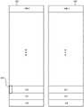
图4B描绘了表示竖直列的多个圆圈。竖直列中的每个包括多个选择晶体管和多个存储器单元。在一个实施方案中,每个竖直列实现一个NAND串。例如,图4B描绘了竖直列422、432、442和452。竖直列422实现NAND串482。竖直列432实现NAND串484。竖直列442实现NAND串486。竖直列452实现NAND串488。下面提供了竖直列的更多细节。由于图4B中描绘的块在箭头330的方向上和在箭头332的方向上延伸,因此该块包括比图4B中描绘的更多的竖直列Figure 4B depicts a plurality of circles representing vertical columns. Each of the vertical columns includes multiple select transistors and multiple memory cells. In one embodiment, each vertical column implements one NAND string. For example, FIG. 4B depicts
图4B还描绘了一组位线415,包括位线411、412、413、414、…、419。图4B示出了二十四个位线,因为仅示出了该块的一部分。设想的是,多于二十四个位线连接到该块的竖直列。表示竖直列的每个圆圈都有一个“x”以指示其与一个位线连接。例如,位线414连接到竖直列422、432、442和452。FIG. 4B also depicts a set of
图4B中描绘的块包括一组局部互连402、404、406、408和410,该组局部互连将各个层连接到在竖直列下方的源极线。局部互连402、404、406、408和410还用于将块的每个层分为四个区域;例如,图4B中描绘的顶层被分为区域420、430、440和450,这些区域被称为指状部。在实现存储器单元的块的层中,这四个区域被称为字线指状部,它们被局部互连分开。在一个实施方案中,在块的公共级上的字线指状部在块的端部处连接在一起以形成单一字线。在另一个实施方案中,在同一级上的字线指状部不连接在一起。在一个示例性实施方式中,位线仅连接到区域420、430、440和450中的每个中的一个竖直列。在该实施方式中,每个块具有十六行活动列,并且每个位线连接到每个块中的四个行。在一个实施方案中,连接到公共位线的所有四个行都连接到同一字线(经由连接在一起的在同一级上的不同字线指状部);因此,系统使用源极侧选择线和漏极侧选择线来选择四个中的要进行存储器操作(编程、验证、读取和/或擦除)的一个(或另一个子集)。The block depicted in Figure 4B includes a set of
尽管图4B示出了在一个块中每个区域具有四行竖直列,四个区域就有十六行竖直列,但是这些确切数字是示例性实施方式。其他实施方案可以包括每一块更多或更少的区域、每一区域更多行或更少行的竖直列、以及每一块更多行或更少行的竖直列。Although FIG. 4B shows that each region in a block has four rows of vertical columns, there are sixteen rows of vertical columns for four regions, these exact numbers are exemplary implementations. Other embodiments may include more or fewer regions per block, more or fewer rows of vertical columns per region, and more or fewer rows of vertical columns per block.
图4B还示出了竖直列是交错的。在其他实施方案中,可以使用不同交错模式。在一些实施方案中,竖直列不交错。Figure 4B also shows that the vertical columns are staggered. In other embodiments, different interleaving patterns may be used. In some embodiments, the vertical columns are not staggered.
图4C描绘了三维存储器结构126的实施方案的一部分,其示出了沿图4B的线AA的剖视图。该剖视图切穿竖直列432和434以及区域430(参见图4B)。图4C的结构包括:两个漏极侧选择层SGD0和SGD1;两个源极侧选择层SGS0和SGS1;四个虚设字线层DD0、DD1、DS0以及DS1;以及四十八个数据字线层WLL0至WLL47,该数据字线层用于连接到数据存储器单元。其他实施方案可以实现多于或少于两个的漏极侧选择层、多于或少于两个的源极侧选择层、多于或少于四个的虚设字线层以及多于或少于四十八个的字线层(例如,96个字线层)。竖直列432和434被描绘为突出穿过漏极侧选择层、源极侧选择层、虚设字线层以及字线层。在一个实施方案中,每个竖直列都包括了NAND串。例如,竖直列432包括NAND串484。在竖直列和下面列出的层之下的是基板101、基板上的绝缘膜454以及源极线SL。竖直列432的NAND串在堆叠的底部处具有源极端并在堆叠的顶部处具有漏极端。与图4B一致,图4C示出了经由连接器407连接到位线414的竖直列432。还描绘了局部互连404和406。Figure 4C depicts a portion of an embodiment of a three-
为了易于参照,以下统称为导电层:漏极侧选择层SGD0和SGD;源极侧选择层SGS0和SGS1;虚设字线层DD0、DD1、DS0以及DS1;以及字线层WLL0至WLL47。在一个实施方案中,导电层由TiN和钨的组合制成。在其他实施方案中,可以使用其他材料形成导电层,诸如掺杂的多晶硅、金属(诸如钨或金属硅化物)。在一些实施方案中,不同导电层可以由不同材料形成。在导电层之间的是介电层DL0至DL55。例如,介电层DL47在字线层WLL43上方和字线层WLL44下方。在一个实施方案中,介电层由SiO2制成。在其他实施方案中,可以使用其他介电材料形成介电层。For ease of reference, the following are collectively referred to as conductive layers: drain side selection layers SGD0 and SGD; source side selection layers SGS0 and SGS1; dummy word line layers DD0, DD1, DS0 and DS1; and word line layers WLL0 to WLL47. In one embodiment, the conductive layer is made of a combination of TiN and tungsten. In other embodiments, other materials may be used to form the conductive layer, such as doped polysilicon, metals such as tungsten or metal suicides. In some embodiments, the different conductive layers may be formed of different materials. Between the conductive layers are dielectric layers DL0 to DL55. For example, the dielectric layer DL47 is above the word line layer WLL43 and below the word line layer WLL44. In one embodiment, the dielectric layer is made ofSiO2 . In other embodiments, other dielectric materials may be used to form the dielectric layer.
非易失性存储器单元沿竖直列形成,该竖直列延伸穿过堆叠中的交替的导电层和介电层。在一个实施方案中,存储器单元布置在NAND串中。字线层WLL0至WLL47连接到存储器单元(也被称为数据存储器单元)。虚设字线层DD0、DD1、DS0以及DS1连接到虚设存储器单元。虚设存储器单元不存储主机数据(从主机提供的数据,诸如来自主机的用户的数据),而数据存储器单元有资格存储主机数据。漏极侧选择层SGD0和SGD1用于将NAND串与位线电连接和断开。源极侧选择层SGS0和SGS1用于将NAND串与源极线SL电连接和断开。Non-volatile memory cells are formed along vertical columns extending through alternating conductive and dielectric layers in the stack. In one embodiment, the memory cells are arranged in NAND strings. The word line layers WLL0 to WLL47 are connected to memory cells (also referred to as data memory cells). The dummy word line layers DD0, DD1, DS0, and DS1 are connected to the dummy memory cells. Dummy memory cells do not store host data (data provided from the host, such as data from users of the host), whereas data memory cells are eligible to store host data. The drain side selection layers SGD0 and SGD1 are used to electrically connect and disconnect the NAND strings from the bit lines. The source side selection layers SGS0 and SGS1 are used to electrically connect and disconnect the NAND strings from the source lines SL.
图4D描绘了图4C中部分地描绘的块的导电层(SGD0、SGD1、SGS0、SGS1、DD0、DD1、DS0、DS1以及WLL0至WLL47)的逻辑表示。SGD层SGD0和SGD0各自包括与一组NAND串的漏极侧相关联的平行选择栅极线行。例如,SGD0包括漏极侧选择栅极区域426、427、428和429。如上面关于图4B所述,在一个实施方案中,局部互连402、404、406、408和410将每个导电层分成四个区域或指状部。在一个实施方案中,在同一级上的四个选择栅极区域被连接在一起。在另一个实施方案中,每个选择栅极区域作为单独选择线操作。Figure 4D depicts a logical representation of the conductive layers (SGDO, SGD1, SGSO, SGS1, DDO, DD1, DS0, DS1, and WLL0 to WLL47) of the block partially depicted in Figure 4C. The SGD layers SGD0 and SGD0 each include a row of parallel select gate lines associated with the drain sides of a set of NAND strings. For example, SGD0 includes drain side
在SGD层下面是漏极侧虚设字线层。在一种方法中,每个虚设字线层表示字线,并且在堆叠中的给定高度处连接到一组虚设存储器单元。例如,DD0包括字线层区域447、449、451和453。虚设存储器单元(也称为非数据存储器单元)不存储数据并且无法存储数据,而数据存储器单元有资格存储数据。此外,虚设存储器单元的Vth通常在制造商时固定或者可以周期性地调整,而数据存储器单元的Vth更频繁地改变,例如,在数据存储器单元的擦除和编程操作期间。Below the SGD layer is the drain side dummy word line layer. In one approach, each dummy word line layer represents a word line and is connected to a set of dummy memory cells at a given height in the stack. For example, DD0 includes word
虚设字线层下面是数据字线层。例如,WLL47包括与图4A一致的字线层区域461、462、463和464。在数据字线层下方的是源极侧虚设字线层DS1和DS0。Below the dummy word line layer is a data word line layer. For example, WLL 47 includes word
源极侧虚设字线层下面是SGS层。SGS层SGS0和SGS1各自包括与一组NAND串的源极侧相关联的平行选择栅极线行。例如,SGS0包括源极侧选择栅极线455、456、457和458。在一种方法中,每个选择栅极线可以被独立地控制。或者,选择栅极线可以被连接并共同地控制。Below the dummy word line layer on the source side is the SGS layer. The SGS layers SGS0 and SGS1 each include a row of parallel select gate lines associated with the source side of a set of NAND strings. For example, SGS0 includes source side
图4E描绘了包括竖直列432的一部分的图4C的区域429的剖视图。在一个实施方案中,竖直列是圆形的并包括四个层;然而,在其他实施方案中,可以包括多于或少于四个层,并且可以使用其他形状。在一个实施方案中,竖直列432包括由诸如SiO2的电介质制成的内芯层470。也可以使用其他材料。包围内芯470的是多晶硅沟道471。也可以使用除了多晶硅之外的材料。需注意,沟道471连接到位线。包围沟道471的是隧穿电介质472。在一个实施方案中,隧穿电介质472具有ONO结构。包围隧穿电介质472的是电荷捕集层473,诸如(例如)氮化硅。也可以使用其他存储器材料和结构。本文所述的技术不限于任何特定材料或结构。FIG. 4E depicts a cross-sectional view of
图4E示出了介电层DLL51、DLL52、DLL53、DLL54和DLL55,还有字线层WLL47、虚设字线层DD0和DD1以及漏极侧选择层SGD0和SGD1。导电层(WLL47、DD0、DD1、SGD0和SGD1)中的每个包括被氧化铝层477包围的导电区域476,该氧化铝层被阻挡氧化物(SiO2)层478包围。需注意,导电层的与竖直列432相邻的部分可以被认为是存储器单元160的控制栅极154或选择栅极162的控制栅极164。氧化铝层477和/或阻挡氧化物(SiO2)层478是阻挡层152的一个示例。字线层与竖直列的物理相互作用形成存储器单元和选择栅极。因此,在一个实施方案中,存储器单元包括沟道471、隧穿电介质472、电荷捕集层473、阻挡氧化物层478、氧化铝层477以及字线区域476。例如,字线层WLL47的一部分和竖直列432的一部分包括存储器单元MC1。虚设字线层DD1的一部分和竖直列432的一部分包括虚设存储器单元DMC1。虚设字线层DD0的一部分和竖直列432的一部分包括虚设存储器单元DMC0。在一个实施方案中,导电层SGD1的一部分和竖直列432的一部分包括漏极侧选择晶体管DSST1。在一个实施方案中,导电层SGD0的一部分和竖直列432的一部分包括漏极侧选择晶体管DSST0。在一些实施方案中,导电层SGD1和SGD0被电连接(图4E中未示出被连接)。在其他架构中,选择栅极和存储器单元可以具有不同结构。4E shows dielectric layers DLL51, DLL52, DLL53, DLL54 and DLL55, as well as word line layer WLL47, dummy word line layers DD0 and DD1, and drain side selection layers SGD0 and SGD1. Each of the conductive layers ( WLL 47 , DD0 , DD1 , SGD0 and SGD1 ) includes a
当对存储器单元进行编程时,电子存储在与存储器单元相关联的电荷捕集层473的一部分中。响应于字线区域476上的适当电压,这些电子通过隧穿电介质472从沟道471被吸引到电荷捕集层473中。存储器单元的阈值电压(Vth)可以与所存储的电荷量成比例地增大。在一个实施方案中,通过电子的福勒-诺得海姆(Fowler-Nordheim)隧穿到电荷捕集层中来实现编程。在擦除操作期间,电子返回到沟道或空穴被注入到电荷捕集层中以与电子重组。在一个实施方案中,使用经由诸如栅极感应的漏极泄漏(GIDL)的物理机制的空穴注入到电荷捕集层中来实现擦除。When a memory cell is programmed, electrons are stored in a portion of the
需注意,数据和虚设存储器单元都可以被编程。在一些实施方案中,虚设存储器单元被擦除,并且在存储器阵列的操作期间保持处于擦除状态。因此,虚设存储器单元可以具有低阈值电压。此外,虚设存储器单元可以在其电荷捕集层中具有大量空穴。Note that both data and dummy memory cells can be programmed. In some embodiments, the dummy memory cells are erased and remain in an erased state during operation of the memory array. Therefore, the dummy memory cells may have low threshold voltages. Additionally, dummy memory cells can have large numbers of holes in their charge trapping layers.
还需注意,选择栅极晶体管也可以类似于对存储器单元进行编程的方式进行编程。在一些实施方案中,选择栅极晶体管被编程为具有用于最佳存储器阵列操作的目标阈值电压。本文公开的实施方案阻止或减小选择栅极晶体管的阈值电压的不期望的变化。Note also that the select gate transistors can also be programmed in a manner similar to programming memory cells. In some implementations, the select gate transistors are programmed to have a target threshold voltage for optimal memory array operation. Embodiments disclosed herein prevent or reduce undesired changes in the threshold voltage of select gate transistors.
图4F示出了跨整个块延伸的物理字线WLL0至WLL47。物理虚设字线DD0和DD1也跨整个块延伸。图4F的结构对应于图4A至图4B的块2中的部分306,包括位线411、412、413、414、…、419。在该块内,每个位线连接到四个NAND串。漏极侧选择线SGD用于确定四个NAND串中的哪一个连接到相关联的位线。还可以考虑将该块划分为四个子块SBA、SBB、SBC以及SBD。FIG. 4F shows physical word lines WLL0 through WLL47 extending across the entire block. Physical dummy word lines DD0 and DD1 also extend across the entire block. The structure of FIG. 4F corresponds to
子块SBA对应于由SGD0A、SGD1A、SGS1A和SGS0A控制的那些竖直NAND串。需注意,SGD0A和SGD1A可以被施加有相同电压。例如,SGD0A和SGD1A可以被电连接(尽管这不是要求的)。同样,SGS0A和SGS1A可以被施加有相同电压。例如,SGS0A和SGDSA可以被电连接(尽管这不是要求的)。Sub-block SBA corresponds to those vertical NAND strings controlled by SGD0A, SGD1A, SGS1A and SGS0A. Note that SGD0A and SGD1A can be applied with the same voltage. For example, SGD0A and SGD1A may be electrically connected (although this is not required). Likewise, SGS0A and SGS1A can be applied with the same voltage. For example, SGS0A and SGDSA may be electrically connected (although this is not required).
子块SBB对应于由SGD0B、SGD1B、SGS1B和SGS0B控制的那些竖直NAND串。需注意,SGD0B和SGD1B可以被施加有相同电压。例如,SGD0B和SGD1B可以被电连接(尽管这不是要求的)。同样,SGS0B和SGS1B可以被施加有相同电压。例如,SGS0B和SGDSB可以被电连接(尽管这不是要求的)。Sub-block SBB corresponds to those vertical NAND strings controlled by SGD0B, SGD1B, SGS1B and SGS0B. Note that SGD0B and SGD1B can be applied with the same voltage. For example, SGD0B and SGD1B may be electrically connected (although this is not required). Likewise, SGS0B and SGS1B can be applied with the same voltage. For example, SGS0B and SGDSB may be electrically connected (although this is not required).
子块SBC对应于由SGD0C、SGD1C、SGS1C和SGS0C控制的那些竖直NAND串。需注意,SGD0C和SGD1C可以被施加有相同电压。例如,SGD0C和SGD1C可以被电连接(尽管这不是要求的)。同样,SGS0C和SGS1C可以一起被控制。例如,SGS0C和SGDSC可以被电连接(尽管这不是要求的)。Sub-block SBC corresponds to those vertical NAND strings controlled by SGD0C, SGD1C, SGS1C and SGSOC. Note that SGD0C and SGD1C can be applied with the same voltage. For example, SGD0C and SGD1C may be electrically connected (although this is not required). Likewise, SGSOC and SGS1C can be controlled together. For example, the SGSOC and SGDSC may be electrically connected (although this is not required).
子块SBD对应于由SGD0D、SGD1D、SGS1D以及SGS0D控制的那些竖直NAND串。需注意,SGD0D和SGD1D可以被施加有相同电压。例如,SGD0D和SGD1D可以被电连接(尽管这不是要求的)。同样,SGS0D和SGS1D可以一起被控制。例如,SGS0D和SGS1D可以被电连接(尽管这不是要求的)。Sub-block SBD corresponds to those vertical NAND strings controlled by SGD0D, SGD1D, SGS1D, and SGS0D. Note that SGD0D and SGD1D can be applied with the same voltage. For example, SGD0D and SGD1D may be electrically connected (although this is not required). Likewise, SGS0D and SGS1D can be controlled together. For example, SGS0D and SGS1D may be electrically connected (although this is not required).
需注意,每个SGD0A可以对应于图4D中的区域426。同样,每个SGD0B可以对应于图4D中的区域427。同样,每个SGD0C可以对应于图4D中的区域428。同样,每个SGD0D可以对应于图4D中的区域429。需注意,每个SGS0A可以对应于图4D中的区域455。同样,每个SGS0B可以对应于图4D中的区域455。同样,每个SGS0C可以对应于图4D中的区域456。同样,每个SGS0D可以对应于图4D中的区域457。Note that each SGD0A may correspond to
另外地,需注意,在图4F的示意图中,所描绘的各个存储器单元具有两个“栅极”。存储器单元栅极中的一个是控制栅极154,另一个“栅极”是指电荷捕集区域473。选择晶体管被描绘为具有单个栅极(例如,控制栅极164),以帮助示出选择栅极与存储器单元之间的区别。需注意,选择晶体管还可以具有电荷捕集区域。此外,该电荷捕集材料可以与存储器单元共用。例如,图1C示出了作为由存储器单元160和选择栅极162共用的连续区域的电荷捕集材料473。同样,图4E将电荷捕集材料473描绘为由数据存储器单元MC1、虚设存储器单元DMC1、DMC2以及选择栅极晶体管SGD1、SGD0共用的连续区域。Additionally, note that in the schematic diagram of Figure 4F, each memory cell depicted has two "gates." One of the memory cell gates is the
虽然图4至图4F的示例性存储器系统是包括具有电荷捕集材料的竖直NAND串的三维存储器结构,但是其他(2D和3D)存储器结构也可以与本文所述的技术一起使用。例如,也可以使用浮栅存储器(例如,NAND型和NOR型闪存存储器)、ReRAM存储器、磁阻存储器(例如,MRAM)和相变存储器(例如,PCRAM)。Although the exemplary memory system of FIGS. 4-4F is a three-dimensional memory structure including vertical NAND strings with charge trapping material, other (2D and 3D) memory structures may also be used with the techniques described herein. For example, floating gate memory (eg, NAND-type and NOR-type flash memory), ReRAM memory, magnetoresistive memory (eg, MRAM), and phase-change memory (eg, PCRAM) may also be used.
ReRAM存储器的一个示例包括可逆电阻切换元件,其布置在由X线和Y线(例如,字线和位线)访问的交叉点阵列中。在另一个实施方案中,存储器单元可包括导电桥存储器元件。导电桥存储器元件也可称为可编程金属化单元。基于固体电解质内的离子的物理重新定位,导电桥存储器元件可用作状态改变元件。在一些情况下,导电桥存储器元件可包括两个固体金属电极,一个是相对惰性的(例如,钨),而另一个是电化学活性的(例如,银或铜),在两个电极之间具有固体电解质的薄膜。随着温度升高,离子的迁移率也增加,这导致导电桥存储器单元的编程阈值降低。因此,导电桥存储器元件可在整个温度范围内具有宽范围的编程阈值。One example of a ReRAM memory includes reversible resistance-switching elements arranged in a cross-point array accessed by X and Y lines (eg, word lines and bit lines). In another embodiment, the memory cells may include conductive bridge memory elements. Conductive bridge memory elements may also be referred to as programmable metallization cells. Conductive bridge memory elements can be used as state change elements based on the physical relocation of ions within the solid electrolyte. In some cases, the conductive bridge memory element may include two solid metal electrodes, one relatively inert (eg, tungsten) and the other electrochemically active (eg, silver or copper), between the two electrodes Thin films with solid electrolytes. As the temperature increases, the mobility of the ions also increases, which leads to a decrease in the programming threshold of the conductive bridge memory cells. Thus, conductive bridge memory elements can have a wide range of programming thresholds over the entire temperature range.
磁阻存储器(MRAM)通过磁存储元件存储数据。元件由两个铁磁板形成,每个铁磁板可保持磁化,由薄的绝缘层隔开。两个板中的一个是设置为特定极性的永磁体;可以改变另一个板的磁化以匹配外磁场的磁化来存储内存。该配置称为自旋阀,并且是MRAM位的最简单结构。存储器设备由此类存储器单元的网格构建。在用于编程的一个实施方案中,每个存储器单元位于一对写入线之间,该对写入线被布置成彼此成直角,与单元平行,一个在单元上方并且一个在单元下方。当电流通过它们时,产生感应磁场。Magnetoresistive memory (MRAM) stores data through magnetic storage elements. The element is formed from two ferromagnetic plates, each of which holds the magnetization, separated by a thin insulating layer. One of the two plates is a permanent magnet set to a specific polarity; the magnetization of the other plate can be changed to match that of the external magnetic field to store the memory. This configuration is called a spin valve and is the simplest structure of an MRAM bit. A memory device is constructed from a grid of such memory cells. In one embodiment for programming, each memory cell is located between a pair of write lines arranged at right angles to each other, parallel to the cell, one above and one below the cell. When current is passed through them, an induced magnetic field is created.
相变存储器(PCRAM)利用了硫属化物玻璃的独特行为。一个实施方案使用GeTe-Sb2Te3超晶格通过仅利激光脉冲(或来自另一个源的光脉冲)改变锗原子的配位状态来实现非热相变。因此,编程的剂量是激光脉冲。可以通过阻止存储器单元接收光来抑制存储器单元。应当注意,在该文件中使用“脉冲”不需要正方形脉冲,但包括声音、电流、电压光或其他波的(连续或非连续)振动或脉冲串。Phase change memory (PCRAM) takes advantage of the unique behavior of chalcogenide glasses. One embodiment uses a GeTe-Sb2Te3 superlattice to achieve athermal phase transitions by only changing the coordination state of germanium atoms with laser pulses (or light pulses from another source). Therefore, the programmed dose is a laser pulse. Memory cells can be inhibited by preventing them from receiving light. It should be noted that the use of "pulse" in this document does not require square pulses, but includes (continuous or discontinuous) vibrations or pulse trains of sound, current, voltage light or other waves.
上面讨论的存储器系统可以被擦除、编程和读取。在成功编程过程(具有验证)结束时,在适当时,存储器单元的阈值电压应当在用于经编程的存储器单元的阈值电压的一个或多个分布内或在经擦除的存储器单元的阈值电压的分布内。图5示出了当每个存储器单元存储三位数据时用于存储器单元阵列的示例性阈值电压分布。然而,其他实施方案可以使用每一存储器单元其他数据容量(例如,诸如每一存储器单元一位数据、二位数据、四位数据或五位数据)。图5示出了八个阈值电压分布,其对应于八个数据状态。第一阈值电压分布(数据状态)S0表示被擦除的存储器单元。其他七个阈值电压分布(数据状态)S1至S7表示被编程的存储器单元,并且因此也被称为经编程的状态。每个阈值电压分布(数据状态)对应于一组数据位的预确定值。编程到存储器单元中的数据与该单元的阈值电压电平之间的具体关系取决于该单元所采纳的数据编码方案。在一个实施方案中,使用格雷码分配将数据值分配到阈值电压范围,使得如果存储器的阈值电压错误地移位到其相邻物理状态,那么将仅影响一个位。The memory systems discussed above can be erased, programmed and read. At the end of a successful programming process (with verify), the threshold voltages of the memory cells should be within one or more distributions of threshold voltages for programmed memory cells or within the threshold voltages of erased memory cells, as appropriate within the distribution. Figure 5 shows an exemplary threshold voltage distribution for an array of memory cells when each memory cell stores three bits of data. However, other implementations may use other data capacities per memory cell (eg, such as one bit of data, two bits of data, four bits of data, or five bits of data per memory cell). Figure 5 shows eight threshold voltage distributions, which correspond to eight data states. The first threshold voltage distribution (data state) S0 represents erased memory cells. The other seven threshold voltage distributions (data states) S1 to S7 represent programmed memory cells and are therefore also referred to as programmed states. Each threshold voltage distribution (data state) corresponds to a predetermined value for a set of data bits. The specific relationship between the data programmed into a memory cell and the threshold voltage level of the cell depends on the data encoding scheme adopted for the cell. In one embodiment, Gray code assignment is used to assign data values to a range of threshold voltages such that if the threshold voltage of the memory is erroneously shifted to its adjacent physical state, only one bit will be affected.
图5还示出了七个读取参考电压Vr1、Vr2、Vr3、Vr4、Vr5、Vr6以及Vr7,以用于从存储器单元读取数据。通过测试(例如,执行感测操作)给定存储器单元的阈值电压是高于还是低于七个读取参考电压,系统可以确定存储器单元所处于的数据状态(即,S0、S1、S2、S3、…)。Figure 5 also shows seven read reference voltages Vr1, Vr2, Vr3, Vr4, Vr5, Vr6 and Vr7 for reading data from memory cells. By testing (eg, performing a sensing operation) whether the threshold voltage of a given memory cell is above or below the seven read reference voltages, the system can determine which data state the memory cell is in (ie, S0, S1, S2, S3 ,…).
图5还示出了七个验证参考电压Vv1、Vv2、Vv3、Vv4、Vv5、Vv6和Vv7。当将存储器单元编程为数据状态S1时,系统将测试这些存储器单元是否具有大于或等于Vv1的阈值电压。当将存储器单元编程为数据状态S2时,系统将测试存储器单元是否具有大于或等于Vv2的阈值电压。当将存储器单元编程为数据状态S3时,系统将确定存储器单元是否具有大于或等于Vv3的阈值电压。当将存储器单元编程为数据状态S4时,系统将测试这些存储器单元是否具有大于或等于Vv4的阈值电压。当将存储器单元编程为数据状态S5时,系统将测试这些存储器单元是否具有大于或等于Vv5的阈值电压。当将存储器单元编程为数据状态S6时,系统将测试这些存储器单元是否具有大于或等于Vv6的阈值电压。当将存储器单元编程为数据状态S7时,系统将测试这些存储器单元是否具有大于或等于Vv7的阈值电压。Figure 5 also shows seven verify reference voltages Vv1, Vv2, Vv3, Vv4, Vv5, Vv6 and Vv7. When programming memory cells to data state S1, the system will test whether the memory cells have a threshold voltage greater than or equal to Vv1. When programming a memory cell to data state S2, the system will test whether the memory cell has a threshold voltage greater than or equal to Vv2. When programming a memory cell to data state S3, the system will determine whether the memory cell has a threshold voltage greater than or equal to Vv3. When programming memory cells to data state S4, the system will test whether the memory cells have a threshold voltage greater than or equal to Vv4. When programming memory cells to data state S5, the system will test whether the memory cells have a threshold voltage greater than or equal to Vv5. When programming memory cells to data state S6, the system will test whether the memory cells have a threshold voltage greater than or equal to Vv6. When programming memory cells to data state S7, the system will test whether the memory cells have a threshold voltage greater than or equal to Vv7.
图6A是描述由控制器122执行的用于编程的过程的一个实施方案的流程图。在一些实施方案中,主机可以执行控制器的功能,而不是具有专用控制器。在步骤602中,控制器122将指令发送到一个或多个存储器管芯108以对数据进行编程。在步骤604中,控制器122将一个或多个地址发送到一个或多个存储器管芯108。一个或多个逻辑地址指示在何处对数据进行编程。在步骤606中,控制器122将要编程的数据发送到一个或多个存储器管芯108。在步骤608中,控制器122从一个或多个存储器管芯108接收该编程的结果。示例性结果包括成功地对数据进行编程、表明编程操作失败的指示以及表明数据已经被编程但在不同位置处的指示,或者其他结果。在步骤610中,响应于在步骤608中接收到的结果,控制器122更新其维护的系统信息。在一个实施方案中,系统维护指示每个块的状态信息的数据表。该信息可以包括逻辑地址到物理地址的映射、哪些块/字线打开/关闭(或部分地打开/关闭)、哪些块/字线是坏的等。FIG. 6A is a flowchart describing one embodiment of a process performed by the
在一些实施方案中,在步骤602之前,控制器122将会接收主机数据和来自主机的编程指令,并且控制器将会运行ECC引擎224以从主机数据创建码字,如本领域中已知并将在下文更多地描述。这些码字是在步骤606中传输的数据。控制器还可以对数据进行加密以实现相对于存储器单元的磨损均衡。In some embodiments, prior to step 602, the
图6B是描述用于编程的过程的一个实施方案的流程图。图6B的过程由存储器管芯响应于图6A的步骤(即,响应于来自控制器122的指令、数据和地址)而执行。在一个示例性实施方案中,图6B的过程在状态机112的指引下使用上面讨论的一个或多个控制电路在存储器管芯108上执行。图6B的过程也可以用来实现上面讨论的全序列编程。另外地,图6B的过程可以用于实现多阶段编程过程中的每个阶段。Figure 6B is a flowchart describing one embodiment of a process for programming. The process of FIG. 6B is performed by the memory die in response to the steps of FIG. 6A (ie, in response to instructions, data, and addresses from controller 122). In one exemplary embodiment, the process of FIG. 6B is executed on memory die 108 under the direction of
通常,在编程操作期间(经由所选择的字线)施加到控制栅极的编程电压被施加为一系列编程脉冲。在编程脉冲之间的是一组验证脉冲以执行验证。在许多实施方式中,编程脉冲的幅值随每个连续脉冲而增大预确定的步长。在图6B的步骤660中,将编程电压(Vpgm)初始化为起始幅值(例如,约12V至16V,或另一个合适的电平),并且将由状态机112维持的编程计数器PC初始化为1。在步骤662中,将编程信号Vpgm的编程脉冲施加到所选择的字线(被选择用于编程的字线)。在一个实施方案中,被同时地编程的一组存储器单元全部都连接到同一字线(所选择的字线)。未选择的字线接收一个或多个升压电压(例如,约6伏至11伏)以执行本领域中已知的升压方案。如果存储器单元应当进行编程,那么对应位线接地。另一方面,如果存储器单元应当保持在其当前阈值电压,那么对应位线连接到Vdd以禁止编程。在步骤662中,将编程脉冲同时地施加到连接到所选择的字线的所有存储器单元,使得同时地对连接到所选择的字线的所有存储器单元进行编程。也就是说,它们在同一时间上或在重叠时间期间(两者都被视为是同时的)进行编程。以此方式,除非已经将它们锁定以阻止进行编程,否则连接到所选择的字线的所有存储器单元将同时地具有其阈值电压变化。Typically, the programming voltage applied to the control gate (via a selected word line) during a programming operation is applied as a series of programming pulses. Between the programming pulses is a set of verify pulses to perform verification. In many embodiments, the amplitude of the programming pulses increases by a predetermined step size with each successive pulse. In
在步骤664中,使用一组适当验证参考电压以执行一个或多个验证操作来验证适当存储器单元。在一个实施方案中,通过应用被选择用于编程的存储器单元的阈值电压是否已经达到适当验证参考电压的测试来执行验证过程。In
在步骤666中,确定是否所有存储器单元都已经达到其目标阈值电压(通过)。若是如此,那么编程过程完成并是成功的,因为所有选择的存储器单元都被编程并验证了其目标状态。在步骤668中,报告状态“通过”。如果在666中确定不是所有存储器单元都已经达到其目标阈值电压(失败),那么编程过程将继续到步骤680。In
在步骤680中,该系统对尚未达到其相应的目标阈值电压分布的存储器单元的数量进行计数。即,该系统对目前为止验证过程已经失败的存储器单元的数量进行计数。该计数可以由状态机、控制器或其他逻辑来完成。在一个实施方式中,感测块中的每个将存储其相应的单元的状态(通过/失败)。在一个实施方案中,存在一个总计数,其反映了最后一个验证步骤已经失败的当前正在编程的存储器单元的总数。在另一个实施方案中,为每个数据状态保留单独计数。In
在步骤682中,确定来自步骤680的计数是否小于或等于预确定的极限。在一个实施方案中,预确定的极限是在存储器单元的页面的读取过程期间可通过纠错码(ECC)校正的位的数量。如果失败的存储器单元的数量小于或等于预确定的极限,那么编程过程可以停止并在步骤668中报告“通过”状态。在这种情况下,足够的存储器单元被正确地编程,使得可以在读取过程期间使用ECC来校正校正尚未完全地编程的剩余几个存储器单元。在一些实施方案中,步骤680将针对每个扇区、每个目标数据状态或其他单元对失败的单元的数量进行计数,并且在步骤682中将这些计数单独地或共同地与阈值进行比较。In
在另一个实施方案中,预确定的极限可以小于在读取过程期间可由ECC校正的位的数量以考虑导未来错误。当对页面的少于所有的存储器单元进行编程、或比较仅一个数据状态(或少于所有的状态)的计数时,预确定的极限就可以是在存储器单元的页面的读取过程期间ECC可校正的位的数量的一部分(按比例或不按比例)。在一些实施方案中,该极限不是预确定的。相反,它基于已经为页面计数的错误数量、所执行的编程擦除周期数量或其他标准来改变。In another embodiment, the predetermined limit may be less than the number of bits that can be corrected by ECC during the read process to account for future errors. When programming less than all memory cells of a page, or comparing counts of only one data state (or less than all states), the predetermined limit may be that the ECC may be available during a read process of a page of memory cells The fraction of the number of bits corrected (scaled or not). In some embodiments, this limit is not predetermined. Rather, it varies based on the number of errors that have been counted for the page, the number of program-erase cycles performed, or other criteria.
如果失败的存储器单元的数量不小于预确定的极限,那么编程过程在步骤684处继续并对照编程极限值(PL)检查编程计数器PC。编程极限值的示例包括12、20和30;然而,可以使用其他值。如果编程计数器PC不小于编程极限值PL,那么认为编程过程已经失败并在步骤688中报告失败状态。这是编程故障的一个示例。如果编程计数器PC小于编程极限值PL,那么过程在步骤686处继续,在此期间,编程计数器PC递增了1,并且编程电压Vpgm被提高到下一量值。例如,下一脉冲将具有比前一脉冲大一个步长(例如,0.1伏至0.5伏的步长)的幅值。在步骤686之后,该过程循环回到步骤662,并且另一个编程脉冲被施加到所选择的字线,使得执行图6B的编程过程的另一个迭代(步骤662至686)。If the number of failed memory cells is not less than the predetermined limit, the programming process continues at
一般来讲,在验证操作和读取操作期间,将所选择的字线连接到电压(参考信号的一个示例),该电压的电平针对每个读取操作(例如,参见图5的读取比较电平Vr1、Vr2、Vr3、Vr4、Vr5、Vr6和Vr7)或验证操作(例如,参见图5的验证目标电平Vv1、Vv2、Vv3、Vv4、Vv5、Vv6和Vv7)指定,以便确定相关存储器单元的阈值电压是否已经达到这个水平。在施加字线电压之后,测量存储器单元的传导电流以确定该存储器单元是否响应于施加到字线的电压而接通(被传导电流)。如果传导电流被测量为大于特定值,那么假设存储器单元被接通并且施加到字线的电压大于存储器单元的阈值电压。如果传导电流未测量为大于特定值,那么假设存储器单元未接通并且施加到字线的电压不大于存储器单元的阈值电压。在读取或验证过程期间,未选择的存储器单元在其控制栅极处被提供了一个或多个读取通过电压,使得这些存储器单元将作为通过栅极操作(例如,不管这些存储器单元是被编程还是被擦除都传导电流)。In general, during verify and read operations, the selected word line is connected to a voltage (an example of a reference signal) at a level for each read operation (see, eg, the read of FIG. 5 ). Compare levels Vr1, Vr2, Vr3, Vr4, Vr5, Vr6, and Vr7) or verify operation (see, for example, verify target levels Vv1, Vv2, Vv3, Vv4, Vv5, Vv6, and Vv7 of Figure 5) designation in order to determine the correlation Whether the threshold voltage of the memory cell has reached this level. After the word line voltage is applied, the conduction current of the memory cell is measured to determine whether the memory cell turns on (conducts current) in response to the voltage applied to the word line. If the conduction current is measured to be greater than a certain value, it is assumed that the memory cell is turned on and the voltage applied to the word line is greater than the threshold voltage of the memory cell. If the conduction current is not measured to be greater than a certain value, then it is assumed that the memory cell is not turned on and the voltage applied to the word line is not greater than the threshold voltage of the memory cell. During a read or verify process, unselected memory cells are provided with one or more read pass voltages at their control gates such that these memory cells will operate as pass gates (eg, regardless of whether the memory cells are Whether programming or erasing conducts current).
有许多方法来在读取或验证操作期间测量存储器单元的传导电流。在一个示例中,以存储器单元对感测放大器中的专用电容器放电或充电的速率来测量该存储器单元的传导电流。在另一个示例中,所选择的存储器单元的传导电流允许(或不允许)包括存储器单元的NAND串对对应位线放电。在某时间段之后测量位线上的电压,以查看其是否已经放电。需注意,本文所述的技术可以与本领域中已知的用于验证/读取的不同方法一起使用。也可以使用本领域中已知的其他读取和验证技术。There are many ways to measure the conduction current of a memory cell during a read or verify operation. In one example, the conduction current of a memory cell is measured as the rate at which the memory cell discharges or charges a dedicated capacitor in the sense amplifier. In another example, the conduction current of the selected memory cell allows (or does not allow) the NAND string comprising the memory cell to discharge the corresponding bit line. The voltage on the bit line is measured after a certain period of time to see if it has discharged. Note that the techniques described herein can be used with different methods known in the art for verification/reading. Other reading and verification techniques known in the art can also be used.
在一些实施方案中,控制器122从主机(或客户端、用户等)接收请求以将主机数据(从主机接收的数据)编程到存储器系统中。在一些实施方案中,控制器122将要编程的主机数据布置到数据单元中。例如,控制器122可以将主机数据布置到页面、字线单元、块、巨型块或其他单元中。In some embodiments, the
图7A是向存储器单元的块(块0、…、块m-1)提供电压的行解码器124的一个实施方案的简化示意图。块可以全部在同一平面上,如在图4A的示例中的那样。每个块具有许多导线(SGD、DD、WLL0至WLLn、DS以及SGS)。导线是本文提出的架构示例中的一些的简化。需注意,由于常用术语“选择线”和“字线”,因此使用术语“线”。然而,将了解,导“线”不限于几何形线,而可以具有多种几何形状。导线可以另选地称为导电区域。行解码器124具有晶体管702、704、706、708、710以向导线提供电压。通过向导线提供电压,向数据存储器单元、虚设存储器单元和选择晶体管的控制栅极提供电压,这视情况而定。7A is a simplified schematic diagram of one embodiment of a
块选择线(BLKSEL 720)用于控制晶体管702至710。在该示例中,一对块选择线(BLKSEL 720,BLKSELn 722)与每个块相关联。为了选择块,BLKSEL 720可以为高。这可以接通晶体管702至710,这取决于施加到其他端子的电压。为了未选择的块,BLKSEL 720可以为低。这可以关断晶体管702至710,这取决于施加到其他端子的电压。需注意,通常一次只选择平面中的一个块。A block select line (BLKSEL 720 ) is used to control transistors 702-710. In this example, a pair of block select lines (
为了向导线SGD提供选择栅极电压Vsgd,可以使用BLKSEL 720接通漏极选择栅极(或选择线)开关晶体管702,同时向开关晶体管702的漏极提供Vsgs。如所指出,SGD是本文提出的架构示例的简化。SGD可以表示图4C或图4D中的SGD0或SGD1。作为另一个示例,SGD可以表示图4F中的SGD0A、SGD0B、SGD0C或SGD0D。在一些实施方案中,选择一个选择栅极线(在所选择的块中),而不选择其他选择栅极线(在所选择的块中)。例如,参照图4F,可以选择SDG0A,而不选择SDG0B、SDG0C和SDG0D。同时,可以选择SDG1A,而不选择SDG1B、SDG1C和SDG1D。因此,行解码器124可以具有附加开关晶体管702以向块中的其他选择栅极线提供其他选择栅极电压Vsgd。图7B描绘了具有附加开关晶体管702的一个实施方案。To provide select gate voltage Vsgd to conductor SGD,
现在参照图7A,为了向导线DD提供虚设字线电压Vdum_WL,可以使用BLKSEL 720接通漏极虚设字线开关晶体管704,同时向开关晶体管704的漏极提供Vdum_WL。漏极虚设字线开关晶体管704也可以被称为漏极虚设控制栅极开关晶体管704,或更简称为漏极虚设开关晶体管704。相对于图4C至图4F,导线DD可以表示虚设字线层DD0或DD1。为了向导线DS提供虚设字线电压Vdum_WL,可以使用BLKSEL 720接通源极虚设开关晶体管708,同时向开关晶体管708的漏极提供Vdum_WL。相对于图4C至图4F,导线DS可以表示虚设字线层DS0或DS1。因此,行解码器124可以具有附加开关晶体管704、708以向块中的其他虚设字线提供电压。Referring now to FIG. 7A , to provide dummy word line voltage Vdum_WL to conductor DD,
为了向导线WL0至WLn中的一个提供数据字线电压Vdata_WL,可以使用BLKSEL 720接通数据字线开关晶体管706(0)至706(n),同时向开关晶体管706(0)至706(n)的相应漏极提供Vdata_WL。数据字线开关晶体管706也可以被称为数据控制栅极开关晶体管706,或更简称为数据开关晶体管706。对于不同数据字线,Vdata_WL的量值可以不同。相对于图4C至图4F,导线WL0至WLn可以表示字线层WLL0至WLL47。To provide the data word line voltage Vdata_WL to one of the conductors WL0 through WLn,
为了向导线SGS提供选择栅极电压Vsgs,可以使用BLKSEL 720接通源极选择栅极(或选择线)开关晶体管710,同时向开关晶体管710的漏极提供Vsgs。在图4C或图4D中,SGS可以表示SGS0或SGS1。作为另一个示例,SGS可以表示图4F中的SGS0A、SGS0B、SGS0C或SGS0D。在一些实施方案中,选择一个选择栅极线(在所选择的块中),而不选择其他选择栅极线(在所选择的块中)。例如,参照图4F,可以选择SGS0A,而不选择SGS0B、SGS0C和SGS0D。同时,可以选择SGS1A,而不选择SGS1B、SGS1C和SGS1D。因此,行解码器124可以具有附加开关晶体管710以向块中的其他选择栅极线提供其他选择栅极电压VSGS。To provide select gate voltage Vsgs to conductor SGS,
各个开关晶体管702至710用于实现开关以向相应块中的导线提供电压。在该示例中,对于每个导线的开关,描绘了单一晶体管。然而,在每个导线的开关中可以包括多于一个晶体管以及其他电路元件。Each switching transistor 702-710 is used to implement a switch to provide voltage to the wires in the corresponding block. In this example, a single transistor is depicted for each wire's switch. However, more than one transistor and other circuit elements may be included in the switch of each wire.
需注意,向数据字线提供电压的开关可以另选地称为数据字线开关、数据存储器单元控制栅极开关、或更简称为数据控制栅极开关。同样,向虚设字线提供电压的开关也可以被称为虚设字线开关、虚设存储器单元控制栅极开关、或更简称为虚设控制栅极开关。同样,向选择线提供电压的开关可以另选地称为选择线开关、选择晶体管控制栅极开关或称为选择栅极控制栅极开关。Note that the switches that provide voltage to the data word lines may alternatively be referred to as data word line switches, data memory cell control gate switches, or more simply, data control gate switches. Likewise, switches that provide voltage to dummy word lines may also be referred to as dummy word line switches, dummy memory cell control gate switches, or more simply dummy control gate switches. Likewise, a switch that provides a voltage to a select line may alternatively be referred to as a select line switch, a select transistor controlled gate switch, or a select gate controlled gate switch.
需注意,在一些情况下,行解码器124中的开关可以操作,使得导线处于浮动电压。在一些实施方案中,行解码器中的晶体管被关断以使块中的导线浮动。在一个实施方案中,晶体管706(0)至706(n)被关断以使数据字线WL0至WLn浮动。在一个实施方案中,晶体管704和/或708被关断以使虚设字线DD和/或DS浮动。在一个实施方案中,晶体管702被关断以使漏极侧选择线SGD浮动。在一个实施方案中,晶体管708被关断以使源极侧选择线SGS浮动。在一个实施方案中,可以通过经由BLKSEL 720向晶体管的栅极施加合适的电压来关断晶体管。将显而易见的是,使块中的导线浮动可以使电连接到该导线的控制栅极浮动。Note that, in some cases, switches in
图7B是向存储器单元的块725中的导线提供电压的行解码器124的一个实施方案的简化示意图。该实施方案与图7A的实施方案的不同之处在于开关晶体管被描绘为用于附加选择线。开关晶体管702a向导线SGDA提供电压;开关晶体管702b向导线SGDB提供电压;开关晶体管702c向导线SGDC提供电压;并且开关晶体管702d向导线SGDD提供电压。参照图4F,导线SGDA可以是SGD0A和/或SGD1A;导线SGDB可以是SGD0B和/或SGD1B;导线SGDC可以是SGD0C和/或SGD1C;导线SGDD可以是SGD0D和/或SGD1D。在一些实施方案中,向SGD0A和SGD1A提供相同电压。同样,可以向SGD0B和SGD1B等提供相同电压。7B is a simplified schematic diagram of one embodiment of a
开关晶体管710a向导线SGSA提供电压;开关晶体管710b向导线SGSB提供电压;开关晶体管710c向导线SGSC提供电压;并且开关晶体管710d向导线SGSD提供电压。参照图4F,导线SGSA可以是SGS0A和/或SGS1A;导线SGSB可以是SGS0B和/或SGS1B;导线SGSC可以是SGS0C和/或SGS1C;导线SGSD可以是SGS0D和/或SGS1D。在一些实施方案中,向SGS0A和SGS1A提供相同电压。同样,可以向SGS0B和SGS1B等提供相同电压。
图8是操作非易失性存储装置的过程800的一个实施方案的流程图。在感测操作之后,过程800可以用于在选择晶体管和与选择晶体管相邻的存储器单元之间生成电场。在感测操作之后,过程800可以用于在选择线和与选择线相邻的字线之间生成电场。过程800可以用于在存储器单元串的漏极端、源极端、或漏极端和源极端两者处生成电场。该串可以是NAND串。在一个实施方案中,NAND串在3D存储器阵列中,诸如本文提供的示例。过程800可以由控制电路执行,该控制电路可以包括但不限于控制电路110、状态机112、解码器114/124/132、功率控制模块116、感测块150、读/写电路128和控制器122。FIG. 8 is a flow diagram of one embodiment of a
步骤802包括向与串选择线相邻的字线(或更简称为“相邻字线”)施加读取通过电压。字线与串选择线相邻意味着在字线与串选择线之间没有其他字线。参照图4C至图4E,相邻字线可以是DD0,而串选择线可以是SGD1。需注意,在一些实施方案中,向SGD1和SGD0施加相同电压。参照图4F,相邻字线可以是DD0,而串选择线可以是SGD1A、SGD1B、SGB1C和/或SGD1D中的任一个。在一些实施方案中,相邻字线是虚设字线。Step 802 includes applying a read pass voltage to a word line (or more simply "adjacent word line") adjacent to the string select line. A word line adjacent to a string select line means that there are no other word lines between the word line and the string select line. 4C to 4E, the adjacent word line may be DD0, and the string select line may be SGD1. Note that in some embodiments, the same voltage is applied to SGD1 and SGD0. Referring to FIG. 4F, the adjacent word line may be DD0, and the string select line may be any one of SGD1A, SGD1B, SGB1C, and/or SGD1D. In some implementations, the adjacent word lines are dummy word lines.
需注意,串选择线可以连接到串选择晶体管的控制栅极。需注意,相邻字线可以连接到与串选择晶体管相邻的存储器单元(或更简称为“相邻存储器单元”)的控制栅极。“相邻存储器单元”是指在相邻存储器单元与串选择晶体管之间没有其他存储器单元。参照图4E,相邻存储器单元可以是DMC0,而串选择晶体管可以是DSST1。因此,步骤802可以包括向相邻存储器单元的控制栅极施加读取通过电压。在一些实施方案中,相邻存储器单元是虚设存储器单元。Note that the string select lines may be connected to the control gates of the string select transistors. Note that adjacent word lines may be connected to the control gates of memory cells adjacent to the string select transistors (or simply "adjacent memory cells"). "Adjacent memory cell" means that there are no other memory cells between the adjacent memory cell and the string select transistor. Referring to FIG. 4E, the adjacent memory cell may be DMC0, and the string select transistor may be DSST1. Thus, step 802 may include applying a read pass voltage to the control gates of adjacent memory cells. In some implementations, the adjacent memory cells are dummy memory cells.
步骤802还可以包括在向相邻字线施加读取通过电压时,向串选择线施加电压。串选择线可以是所选择的块中的所选择的串选择线或未选择的串选择线。例如,假设选择图4F中的子块SBD而未选择子块SBA、SBB和SBC。相邻字线可以是DD0,而所选择的串选择线可以是SGD1D。需注意,在一些实施方案中,向SGD1D和SGD0D施加相同电压。相邻字线可以是DD0,而未选择的串选择线可以是SGD1A、SGD1B和/或SGD1C。由于串选择线可以电连接到串选择晶体管的控制栅极,因此步骤802可以包括向串选择晶体管的控制栅极施加电压。Step 802 may also include applying a voltage to the string select line while applying the read pass voltage to the adjacent word line. The string selection line may be a selected string selection line or an unselected string selection line in the selected block. For example, assume that sub-block SBD in FIG. 4F is selected and sub-blocks SBA, SBB and SBC are not selected. The adjacent word line may be DD0 and the selected string select line may be SGD1D. Note that in some embodiments, the same voltage is applied to SGD1D and SGD0D. The adjacent word line may be DD0, while the unselected string select lines may be SGD1A, SGD1B, and/or SGD1C. Since the string select line may be electrically connected to the control gate of the string select transistor,
步骤804包括感测存储器单元串上的所选择的存储器单元。该感测可以是在编程操作期间的验证操作、或读取操作。步骤804可以包括感测块150中的电路感测所选择的存储器单元的条件,诸如在位线中流动的电流。在一个实施方案中,响应于施加到所选择的存储器单元的控制栅极的读取参考电压而测量所选择的存储器单元的传导电流以确定所选择的存储器单元是否接通(被传导电流)。在读取或验证过程的实施方案期间,未选择的存储器单元的控制栅极在其控制栅极处被提供了读取通过电压,使得这些存储器单元将作为通过栅极来操作(例如,不管这些存储器单元是被编程还是被擦除都传导电流)。虚设存储器单元的控制栅极也接收读取通过电压。Step 804 includes sensing the selected memory cell on the string of memory cells. The sensing may be a verify operation during a program operation, or a read operation. Step 804 may include circuitry in
步骤806包括使相邻字线上的电压从读取通过电压降低到稳态电压。需注意,步骤806可以造成相邻存储器单元的控制栅极上的电压从读取通过电压降低到稳态电压。在一个实施方案中,稳态电压为约接地(例如,Vss)。作为一个示例,DD0上的电压下降到稳态电压。Step 806 includes reducing the voltage on the adjacent word line from the read pass voltage to the steady state voltage. Note that
步骤808包括在使相邻字线上的电压减小到稳态电压之后,增大串选择线上的电压。可以增大电压,而同时在相邻字线上仍然是稳态电压。步骤808可以造成增大选择晶体管的控制栅极上的电压。在一个实施方案中,步骤808包括使串选择线上的电压增大到至少在使与选择栅极相邻的字线在步骤810中浮动之后与选择栅极相邻的字线爬升到的爬升电压。Step 808 includes increasing the voltage on the string select line after reducing the voltage on the adjacent word line to a steady state voltage. The voltage can be increased while still being a steady state voltage on adjacent word lines. Step 808 may result in increasing the voltage on the control gate of the select transistor. In one embodiment,
在一个实施方案中,步骤808包括增大所选择的串选择线上的电压。参照图4F的其中选择子块SBD的示例,可以增大SGD1D上的电压。需注意,SGD0D可能接收与SGD1D相同的电压。In one embodiment,
在一个实施方案中,步骤808包括增大所选择的块中的未选择的串选择线上的电压。参照图4F的其中选择子块SBD的示例,可以增大(未选择的)SGD1A上的电压。需注意,SGD0A可能接收与SGD1A相同的电压。作为另一个示例,可以增大(未选择的)SGD1B上的电压。需注意,SGD0B可能接收与SGD1B相同的电压。作为另一个示例,可以增大(未选择的)SGD1C上的电压。需注意,SGD0C可能接收与SGD1C相同的电压。In one embodiment,
步骤810包括在增大串选择线上的电压之后使串选择线和相邻字线浮动。在一个实施方案中,步骤808包括使串选择线在比相邻字线浮动于的电压高的电压处浮动。在一个实施方案中,步骤808包括使串选择晶体管的控制栅极在比相邻存储器单元的控制栅极浮动于的电压高的电压处浮动。需注意,串选择晶体管和相邻存储器单元可以在具有所选择的存储器单元的串上。然而,串选择晶体管和相邻存储器单元可以在与所选择的串相同的块中的未选择的串上。Step 810 includes floating the string select line and adjacent word lines after increasing the voltage on the string select line. In one embodiment,
步骤810可以造成在串选择线与相邻字线之间的电场。步骤810可以造成在串选择晶体管与相邻存储器单元之间的电场。步骤810可以造成在串选择晶体管的控制栅极与相邻存储器单元的控制栅极之间的电场。Step 810 may cause an electric field between the string select line and the adjacent word line. Step 810 may cause an electric field between the string select transistors and adjacent memory cells. Step 810 may cause an electric field between the control gates of the string select transistors and the control gates of adjacent memory cells.
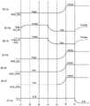
图9A至图9D示出了针对过程800的一个实施方案的在字线和选择线上的示例性电压。图9A示出了相邻字线的电压。图9B示出了其他字线的电压。图9C示出了连接到所选择的NAND串的选择线的电压。例如,图9C示出了所选择的子块中的选择线的电压。图9D示出了连接到与所选择的NAND串共用位线的未选择的NAND串的选择线的电压。例如,图9D示出了未选择的子块的选择线的电压。FIGS. 9A-9D illustrate exemplary voltages on word lines and select lines for one embodiment of
时间t1对应于在过程800的一个实施方案的步骤808之后的条件。图9A示出了在时间t1处相邻字线处于Vss。在一个实施方案中,Vss是接地的。在一个实施方案中,相邻字线是虚设字线。再次参照图4F的示例,相邻字线可以是DD0。图9B示出了在时间t1处其他字线也处于Vss。再次参照图4F的示例,其他字线可以是DS0、DS1、WWL0至WLL47以及DD1。图9C示出了在时间t1处所选择的选择线处于Vsgh。再次参照其中选择子块SBD的示例,所选择的选择线可以是SGD1D。需注意,SGD0D也可以被驱动到Vsgh。图9D示出了在时间t1处未选择的选择线也处于Vsgh。再次参照其中选择子块SBD的示例,未选择的选择线可以是SGD1A、SGD1B和SGD1C。需注意,SGD0A、SGD0B和SGD0C也可以被驱动到Vsgh。需注意,在时间t1处,各个导线被驱动。Time t1 corresponds to the
时间t2对应于当各个导线的浮动开始时的条件。需注意,在字线浮动之后,相邻字线和其他字线上的电压爬升。这在本文中被称为“爬升电压”。在时间t3之后,字线上的电压可以缓慢地放电。需注意,这种放电可能非常缓慢地发生。例如,字线可能花费数十分钟来放电到约Vss。选择线上的电压也可能会缓慢地放电。The time t2 corresponds to the condition when the floating of the respective wires starts. Note that after a word line floats, the voltage on adjacent word lines and other word lines climbs. This is referred to herein as "climb voltage". After time t3, the voltage on the word line can slowly discharge. Note that this discharge can occur very slowly. For example, a word line may take tens of minutes to discharge to about Vss. The voltage on the select line may also discharge slowly.
需注意,在一些实施方案中,Vsgh的量值至少与Vcreep的最大值一样大。在图9A和图9B中,Vcreep在时间t3处处于其最大值。如图9A至图9D所描绘,Vsgh可能在t2与t3之间略微地下降。然而,在一个实施方案中,在时间t3处,Vsgh仍然大于Vcreep。因此,在一些实施方案中,在时间t3处,SGD1D上的电压至少与DD0上的电压一样高。在一些实施方案中,在时间t3处,SGD1A上的电压至少与DD0上的电压一样高。在一些实施方案中,在时间t3处,SGD1B上的电压至少与DD0上的电压一样高。在一些实施方案中,在时间t3处,SGD1C上的电压至少与DD0上的电压一样高。因此,可以生成诸如图1D所示的电场。因此,可以保留各个选择晶体管的阈值电压。Note that in some embodiments, the magnitude of Vsgh is at least as large as the maximum value of Vcreep. In Figures 9A and 9B, Vcreep is at its maximum value at time t3. As depicted in Figures 9A-9D, Vsgh may drop slightly between t2 and t3. However, in one embodiment, at time t3, Vsgh is still greater than Vcreep. Thus, in some embodiments, at time t3, the voltage on SGD1D is at least as high as the voltage on DD0. In some embodiments, at time t3, the voltage on SGD1A is at least as high as the voltage on DDO. In some embodiments, at time t3, the voltage on SGD1B is at least as high as the voltage on DDO. In some embodiments, at time t3, the voltage on SGD1C is at least as high as the voltage on DDO. Therefore, an electric field such as that shown in FIG. 1D can be generated. Therefore, the threshold voltages of the respective selection transistors can be preserved.
此外,选择线上的电压可能在相当长的时间段内保持高于Vcreep。时间t4表示Vcreep已经逐渐地下降到Vcreep最大值的一定分数的任意时间点。这可以是Vcreep最大值的50%、Vcreep最大值的10%等。在一些实施方案中,在时间t4处,选择线上的电压Vsgh仍然大于Vcreep。因此,可以维持诸如图1D所示的电场(但是其量值可能随时间而变化)。因此,可以保留各个选择晶体管的阈值电压。Furthermore, the voltage on the select line may remain above Vcreep for a considerable period of time. Time t4 represents any point in time at which Vcreep has gradually dropped to a certain fraction of the maximum value of Vcreep. This can be 50% of Vcreep max, 10% of Vcreep max, etc. In some implementations, at time t4, the voltage Vsgh on the select line is still greater than Vcreep. Thus, an electric field such as that shown in Figure ID can be maintained (although its magnitude may vary over time). Therefore, the threshold voltages of the respective selection transistors can be preserved.
图10是操作非易失性存储装置的过程1000的一个实施方案的流程图。过程1000说明了过程800的一个实施方案的进一步细节。过程1000可以由控制电路执行,该控制电路可以包括但不限于:控制电路110、状态机112、解码器114/124/132、功率控制模块116、感测块150、读/写电路128和控制器122。图11A至图11G描绘了在过程1000的一个实施方案期间对信号进行定时。然而,过程1000不限于图11A至图11G中描绘的定时。还需注意,图11A至图11G中的时间t1至t7不对应于图9A至9D中的时间t1至t3。10 is a flow diagram of one embodiment of a
过程1000的步骤1002包括建立存储器单元感测条件。这些条件可以用于感测NAND串上的一个存储器单元。可以同时地感测一个或多个NAND串。例如,参照图4F,可以同时地感测与每个位线相关联的零个或一个NAND串。如先前所讨论,可以认为图4F中的块具有四个子块(SBA,SBB,SBC,SBD)。通常,一次选择四个子块中的一个(假设选择该块)。为了讨论,将假设选择子块SBD,并且未选择子块SBA、SBB以及SBC。可以通过向选择晶体管(SGD,SGS)的控制栅极施加合适的电压来选择子块。简单地参照图7B,可以向选择线开关晶体管702a至702d和710a至710d施加电压以向选择晶体管的控制栅极施加合适的电压。而且,块选择线BLKSEL 720可以提供电压以接通开关晶体管702和710。
再次参照图4F,可以通过向位线411至419中的每个施加合适的电压来在步骤1002中选择或不选择位线。选择位线用于选择子块SBD中的NAND串。为了示例,连接到位线411的子块SBD中的NAND串将作为被选择的来讨论。子块SBD中的其他NAND串可能被选择或可能不被选择,这取决于其位线电压。在一个实施方案中,向所选择的选择线和所选择的位线施加的电压的组合将所选择的NAND串连接到位线。Referring again to FIG. 4F, bit lines may be selected or deselected in
而且,为了示例,将使用所选择的NAND串上的WLL46处的存储器单元作为所选择的存储器单元的示例。在步骤1002中,向WLL46施加合适的感测电压。例如,图5中的读取参考电压(Vr1至Vr7)中的一个可适用于WLL46。另选地,图5中的程序验证参考电压(Vv1至Vv7)中的一个可适用于WLL46。需注意,在一些实施方案中,相继地向WLL46施加多达所有参考电压。参照图7B,一个或多个参考电压可以被施加到向WLL46提供电压的字线开关706(46)的漏极。而且,块选择线BLKSEL 720可以提供电压以接通该WL开关晶体管706(46)。Also, for the sake of example, the memory cell at WLL46 on the selected NAND string will be used as an example of the selected memory cell. In
步骤1002还可以包括向未选择的字线以及虚设字线施加读取通过电压。假设导通状态的阈值电压在分配到不同数据状态的阈值电压的范围内,读取通过电压是足以将存储器单元置于导通状态下的电压。参照图7B,可以向虚设字线开关704和708的漏极施加读取通过电压。读取通过电压也可以被施加到除了向所选择的字线提供参考电压的WL开关晶体管706(46)之外的WL开关晶体管706的漏极。而且,块选择线BLKSEL 720可以提供电压以接通虚设字线开关704和708以及其他字线开关706。
图11A至图11F的时序图在时间t1处描绘了针对步骤1002的一个实施方案的导线上的电压。导线在存储器单元的所选择的块中。图11A表示SDG_SEL上的电压,其对应于所选择的子块中的漏极侧选择线。参照图4F,这可以对应于SGD0D和SGD1D。图11A描绘了在时间t1处SGD_SEL上的Vsgd。这可以通过向漏极开关晶体管702d的漏极施加Vsgd来实现。在一些实施方案中,电压Vsgd足够高,以将所选择的NAND串连接到位线。图11G指示了图7B中的开关晶体管702至710是接通还是关断。在时间t1处,所选择的块的行解码器中的所有开关晶体管接通,如图11G所表示。The timing diagrams of FIGS. 11A-11F depict the voltages on the wires at time t1 for one embodiment of
图11D表示了SDS_SEL上的电压,其对应于所选择的子块的源极侧选择线。参照图4F,这可以对应于SGS0D和SGS1D。图11D描绘了在时间t1处SGS_SEL上的Vsgs。这可以通过向源极开关晶体管710d的漏极施加Vsgs来实现。在一些实施方案中,电压Vsgs足够高,以将所选择的NAND串连接到源极线。Figure 1 ID shows the voltage on SDS_SEL, which corresponds to the source side select line of the selected sub-block. Referring to Figure 4F, this may correspond to SGS0D and SGS1D. Figure 1 ID depicts Vsgs on SGS_SEL at time tl. This can be accomplished by applying Vsgs to the drain of
图11B表示了Sel_WL上的电压,其对应于所选择的字线。参照图4F,在本示例中,这可以对应于WLL47。图11B描绘了在时间t1处Sel_WL上的Vcgr。这可以通过向WL开关晶体管706(47)的漏极施加Vcgr来实现。电压Vcgr可以是图5中的参考电压中的一个。FIG. 11B shows the voltage on Sel_WL, which corresponds to the selected word line. Referring to Figure 4F, this may correspond to WLL47 in this example. FIG. 11B depicts Vcgr on Sel_WL at time t1. This can be accomplished by applying Vcgr to the drain of WL switch transistor 706 (47). The voltage Vcgr may be one of the reference voltages in FIG. 5 .
图11C表示了Unsel_WL和DWL上的电压,其对应于未选择的字线和虚设字线。参照图4F,这可以对应于DS0、DSS、WLL0至WLL45、WLL47、DD1以及DD0。图11C描绘了在时间t1处Unsel_WL和DWL上的Vread。这可以通过向WL开关晶体管704,708、WL开关晶体管706(0)至706(45)和706(47)的漏极施加Vread来实现。Figure 11C shows the voltages on Unsel_WL and DWL, which correspond to unselected word lines and dummy word lines. Referring to Figure 4F, this may correspond to DS0, DSS, WLL0 to WLL45, WLL47, DD1 and DD0. FIG. 11C depicts Vread on Unsel_WL and DWL at time t1. This can be accomplished by applying Vread to the drains of
图11E表示了SDG_USEL上的电压,其对应于未选择的子块的漏极侧选择线。参照图4F,这可以对应于SGD0A、SGD1A、SGD0B、SGD1B、SGD0C和SGD1C。图11E描绘了在时间t1处SGD_USEL上的Vss。这可以通过向漏极开关晶体管702a、702b和702c的漏极施加Vss来实现。FIG. 11E shows the voltage on SDG_USEL, which corresponds to the drain-side select line of the unselected sub-block. Referring to Figure 4F, this may correspond to SGD0A, SGD1A, SGD0B, SGD1B, SGD0C, and SGD1C. FIG. 11E depicts Vss on SGD_USEL at time t1. This can be achieved by applying Vss to the drains of
图11F表示了SDS_USEL上的电压,其对应于未选择的子块的源极侧选择线。参照图4F,这可以对应于SGS0A、SGS1A、SGS0B、SGS1B、SGS0C和SGS1C。图11F描绘了在时间t1处SGS_USEL上的Vss。这可以通过向漏极开关晶体管710a、710b和710c的漏极施加Vss来实现。Figure 11F shows the voltage on SDS_USEL, which corresponds to the source side select line of the unselected sub-block. Referring to Figure 4F, this may correspond to SGS0A, SGS1A, SGS0B, SGS1B, SGSOC and SGS1C. FIG. 11F depicts Vss on SGS_USEL at time t1. This can be achieved by applying Vss to the drains of
步骤1004包括感测所选择的存储器单元的条件。在一个实施方案中,响应于施加到所选择的存储器单元的控制栅极的Vcgr而测量所选择的存储器单元的传导电流以确定所选择的存储器单元是否接通(被传导电流)。
步骤1006包括使所选择的存储器单元的控制栅极上的电压增大到Vread。步骤1006可以包括使所选择的WL开关的输入处的电压增大到读取通过电压。图11B在时间t1与时间t3之间描绘了在步骤1006的一个实施方案之后的结果。看到的是,Sel_WL上的电压在时间t1与时间t1之间上升到Vread,并且保持在那里直到时间t4为止。参照图7B,可以使所选择的WL开关706(47)上的电压增大到Vread。
步骤1008包括使存储器单元的控制栅极成低电压。步骤1008可以包括使字线开关的输入下降到低电压。图11B和图11C在时间t4与时间t7之间描绘了在步骤1008的一个实施方案之后的结果。看到的是,Sel_WL上的电压在时间t4与时间t5之间从Vread下降到Vss,并且保持在Vss处直到时间t7为止。同样,Unsel_WL和DWL上的电压在时间t4与时间t5之间从Vread下降到Vss,并且保持在Vss处直到时间t7为止。参照图7B,虚设WL开关704,708以及所有WL开关706的漏极处的电压可以从Vread降低到Vss。需注意,Vss只是低电压的一个示例。在一个实施方案中,Vss是接地的。然而,不要求低电压是接地的。
步骤1010包括使选择晶体管的控制栅极电压增大到高电压。步骤1010可以包括使选择线开关的输入增大到高电压。步骤1010适用于用于所选择的子块和未选择的子块(在所选择的块中)两者的选择线开关。图11A描绘了在时间t5与时间t6之间SGD_SEL上的电压从Vsgd变为VSGH。在时间t6与时间t7之间,SGD_SEL上的电压保持处于VSGH。在时间t7之后,SGD_SEL浮动,这将在下面讨论。图11D描绘了在时间t5与时间t6之间SGS_SEL上的电压从Vsgs变为VSGH。在时间t6与时间t7之间,SGS_SEL上的电压保持处于VSGH。在时间t7之后,SGS_SEL浮动,这将在下面讨论。图11E描绘了在时间t5与时间t6之间SGD_USEL上的电压从Vss变为VSGH。在时间t6与时间t7之间,SGD_USEL上的电压保持处于VSGH。在时间t7之后,SGD_USEL浮动,这将在下面讨论。图11F描绘了在时间t5与时间t6之间SGS_USEL上的电压从Vss变为VSGH。在时间t6和t7之间,SGS_USEL上的电压保持处于VSGH。在时间t7之后,SGS_USEL浮动,这将在下面讨论。
参照图7B,在时间t5处,漏极选择线开关702d的漏极处的电压可以从Vsgd增大到VSGH。参照图7B,在时间t5处,漏极选择线开关702a、702b和702c的漏极处的电压可以从Vss增大到VSGH。参照图7B所示,在时间t5处,源极选择线开关710d的漏极处的电压可以从Vsgs增大到VSGH。参照图7B所示,在时间t5处,源极选择线开关710a、710b和710c的漏极处的电压可以从Vss增大到VSGH。Referring to FIG. 7B, at time t5, the voltage at the drain of the drain
步骤1012包括关断所选择的块的开关晶体管。参照图7B,块选择线BLKSEL 720可以用于关断开关晶体管702至710。图11A至图11G描绘了步骤1012的一个实施方案的结果。在时间t7处,图11G描绘了开关晶体管被关断。在一个实施方案中,这造成了所选择的线中的导线浮动。图11A描绘了SGD_SEL在时间t7之后在VSGH处浮动。图11D描绘了SGS_SEL在时间t7之后在VSGH处浮动。图11E描绘了SGD_USEL在时间t7之后在VSGH处浮动。图11F描绘了SGS_USEL在时间t7之后在VSGH处浮动。
在关断WL开关晶体管后,字线上的电压可以爬升。这在图11B和图11C中由Sel_WL、Unsel_WL以及DWL上的电压在时间t7之后爬升到Vcreep描绘。在一些实施方案中,电压VSGH至少与Vcreep一样高。需注意,图11A至图11G中的时间t7对应于图9A至图9D中的时间t2的一个实施方案。After turning off the WL switch transistor, the voltage on the word line can climb. This is depicted in Figures 11B and 11C by the voltages on Sel_WL, Unsel_WL, and DWL ramping up to Vcreep after time t7. In some embodiments, the voltage VSGH is at least as high as Vcreep. Note that time t7 in FIGS. 11A-11G corresponds to one embodiment of time t2 in FIGS. 9A-9D .
因此,在时间t7之后,可以在选择晶体管与相邻存储器单元之间形成电场。例如,这可以是在NAND串的漏极端或源极端处。电场可以减小或消除电荷捕集材料473中的空穴移动,这可以保留选择晶体管的阈值电压。Therefore, after time t7, an electric field can be formed between the select transistor and the adjacent memory cell. For example, this can be at the drain terminal or the source terminal of the NAND string. The electric field can reduce or eliminate hole movement in the
本文公开的第一实施方案包括装置,该装置包括:NAND串,该NAND串包括非易失性存储器单元;串选择线;多个字线,该多个字线连接到非易失性存储器单元的控制栅极;和控制电路,该控制电路与NAND串、串选择线以及多个字线通信。控制电路被配置为:向与串选择线相邻的字线施加读取通过电压;在感测到NAND串上的所选择的存储器单元之后,使相邻字线上的读取通过电压降低到稳态电压;在使相邻字线上的电压降低到稳态电压之后,增大串选择线上的电压;以及在增大串选择线上的电压之后,使串选择线和相邻字线浮动。A first embodiment disclosed herein includes an apparatus comprising: a NAND string including non-volatile memory cells; a string select line; a plurality of word lines connected to the non-volatile memory cells the control gate; and a control circuit in communication with the NAND string, the string select line, and the plurality of word lines. The control circuit is configured to: apply a read pass voltage to a word line adjacent to the string select line; after sensing the selected memory cell on the NAND string, reduce the read pass voltage on the adjacent word line to steady state voltage; after reducing the voltage on the adjacent word line to the steady state voltage, increasing the voltage on the string select line; and after increasing the voltage on the string select line, floating the string select line and the adjacent word line.
在依据第一实施方案的第二实施方案中,控制电路还被配置为使串选择线上的电压增大到至少在使相邻字线浮动之后相邻字线爬升到的最大爬升电压。In a second implementation in accordance with the first implementation, the control circuit is further configured to increase the voltage on the string select line to at least a maximum ramp-up voltage to which the adjacent word line climbs after floating the adjacent word line.
在依据第一实施方案或第二实施方案的第三实施方案中,控制电路还被配置为使串选择线在比相邻字线浮动于的电压高的电压处浮动。In a third embodiment according to the first embodiment or the second embodiment, the control circuit is further configured to float the string select line at a higher voltage than the voltage at which the adjacent word line floats.
在依据第一实施方案至第三实施方案中任一项的第四实施方案中,多个字线包括数据字线和虚设字线。相邻字线是虚设字线。控制电路还被配置为使数据字线与串选择线和虚设字线一起浮动。In a fourth implementation according to any one of the first to third embodiments, the plurality of word lines includes data word lines and dummy word lines. Adjacent word lines are dummy word lines. The control circuit is also configured to float the data word lines along with the string select lines and the dummy word lines.
在依据第四实施方案的第五实施方案中,使数据字线和虚设字线浮动造成虚设字线上的电压因NAND串沟道与虚设字线之间的电容耦合而爬升到爬升电压。In a fifth implementation in accordance with the fourth implementation, floating the data word line and the dummy word line causes the voltage on the dummy word line to ramp up to a ramped voltage due to capacitive coupling between the NAND string channel and the dummy word line.
在依据第一实施方案至第五实施方案中任一项的第六实施方案中,串选择线是包括NAND串的非易失性存储器单元的块中的未选择的串选择线。In a sixth implementation in accordance with any one of the first to fifth implementations, the string select line is an unselected string select line in a block of non-volatile memory cells that includes a NAND string.
在依据第一实施方案至第五实施方案中任一项的第七实施方案中,串选择线是包括NAND串的非易失性存储器单元的块中的所选择的串选择线。In a seventh implementation in accordance with any one of the first to fifth implementations, the string select line is a selected string select line in a block of non-volatile memory cells that includes a NAND string.
在依据第七实施方案的第八实施方案中,该装置还包括位线,该位线与NAND串相关联。非易失性存储器单元的块还包括:一个或多个未选择的串选择线;以及一个或多个附加NAND串,该一个或多个附加NAND串与位线相关联。多个字线还与一个或多个附加NAND串相关联。附加NAND串中的每个与未选择的串选择线中的一个相关联。控制电路还被配置为:在向相邻字线施加读取通过电压时,向未选择的串选择线中的每个施加未选择电压;在降低相邻字线上的电压之后,增大未选择的串选择线中的每个上的电压;以及在增大的电压在未选择的串选择线中的每个上并且使相邻字线浮动之后,使未选择的串选择线中的每个上的电压浮动。In an eighth embodiment in accordance with the seventh embodiment, the device further includes a bit line associated with the NAND string. The block of non-volatile memory cells also includes: one or more unselected string select lines; and one or more additional NAND strings associated with the bit lines. The multiple word lines are also associated with one or more additional NAND strings. Each of the additional NAND strings is associated with one of the unselected string select lines. The control circuit is further configured to apply an unselected voltage to each of the unselected string select lines when the read pass voltage is applied to the adjacent word lines, and to increase the unselected voltage after lowering the voltage on the adjacent word lines. the voltage on each of the selected string select lines; and after the increased voltage is on each of the unselected string select lines and floating adjacent word lines, causing each of the unselected string select lines The voltage on one floats.
在依据第一实施方案至第八实施方案中任一项的第九实施方案中,NAND串居于三维存储器阵列中。In a ninth embodiment in accordance with any one of the first to eighth embodiments, the NAND strings reside in a three-dimensional memory array.
在依据第一实施方案至第九实施方案中任一项的第十实施方案中,NAND串包括电荷捕集材料,该电荷捕集材料在具有电连接到选择线的控制栅极的选择晶体管和与该选择晶体管相邻的存储器单元之间连续地延伸。In a tenth embodiment in accordance with any one of the first to ninth embodiments, the NAND string includes charge trapping material between select transistors having control gates electrically connected to select lines and The memory cells adjacent to the selection transistor extend continuously.
在依据第一实施方案至第十实施方案中任一项的第十一实施方案中,还包括:串选择线开关,该串选择线开关被配置为将串选择线开关的输入处的电压传送到串选择线;和虚设字线开关,该虚设字线开关被配置为将虚设字线开关的输入处的电压传送到相邻字线。控制电路还被配置为:关断串选择线开关以使串选择线浮动;以及关断虚设字线开关以使虚设字线浮动。In an eleventh embodiment in accordance with any one of the first to tenth embodiments, further comprising: a string select line switch configured to communicate a voltage at an input of the string select line switch to a string select line; and a dummy word line switch configured to pass a voltage at an input of the dummy word line switch to an adjacent word line. The control circuit is also configured to: turn off the string select line switch to float the string select line; and turn off the dummy word line switch to float the dummy word line.
一个实施方案包括操作非易失性存储装置的方法。该方法包括:向串选择晶体管的控制栅极施加选择电压,而同时向与串选择晶体管相邻的存储器单元的控制栅极施加读取通过电压,该相邻存储器单元和该串选择晶体管是NAND串的部分;感测NAND串上的所选择的非易失性存储器单元;在感测到所选择的非易失性存储器单元之后,使相邻存储器单元的控制栅极上的电压从读取通过电压降低到稳态电压;在使相邻存储器单元的控制栅极上的电压降低到稳态电压之后,增大串选择晶体管的控制栅极上的电压;以及在增大串选择晶体管的控制栅极上的电压之后,使串选择晶体管的控制栅极浮动,而同时使相邻存储器单元的控制栅极浮动。One embodiment includes a method of operating a non-volatile memory device. The method includes applying a select voltage to a control gate of a string select transistor while simultaneously applying a read pass voltage to the control gate of a memory cell adjacent to the string select transistor, the adjacent memory cell and the string select transistor being NAND portion of the string; senses the selected non-volatile memory cell on the NAND string; after sensing the selected non-volatile memory cell, causes the voltage on the control gate of the adjacent memory cell to be read from passing the voltage down to the steady state voltage; increasing the voltage on the control gate of the string select transistor after decreasing the voltage on the control gate of the adjacent memory cell to the steady state voltage; and increasing the control gate of the string select transistor After the voltage on , the control gates of the string select transistors are floated while the control gates of the adjacent memory cells are floated.
一个实施方案包括非易失性存储设备,该非易失性存储设备包括:NAND串,该NAND串包括非易失性存储器单元和串选择晶体管;选择装置,该选择装置用于向串选择晶体管的控制栅极施加选择电压而同时向与串选择晶体管相邻的虚设存储器单元的控制栅极施加读取通过电压;感测装置,该感测装置用于感测NAND串上的所选择的非易失性存储器单元;第一电压施加装置,该第一电压施加装置用于在感测到所选择的非易失性存储器单元之后使虚设存储器单元的控制栅极上的电压从读取通过电压降低到稳态电压;第二电压施加装置,该第二电压施加装置用于在使虚设存储器单元的控制栅极上的电压降低到稳态电压之后增大串选择晶体管的控制栅极上的电压;和浮动装置,该浮动装置用于在增大串选择晶体管的控制栅极上的电压之后使串选择晶体管的控制栅极浮动而同时使虚设存储器单元的控制栅极浮动。One embodiment includes a non-volatile memory device comprising: a NAND string comprising non-volatile memory cells and string select transistors; selecting means for selecting the transistors to the string A select voltage is applied to the control gate of the NAND string while a read pass voltage is applied to the control gates of the dummy memory cells adjacent to the string select transistors; sensing means for sensing the selected non- a volatile memory cell; first voltage applying means for causing the voltage on the control gate of the dummy memory cell to change from a read pass voltage after sensing the selected non-volatile memory cell reducing to a steady state voltage; second voltage applying means for increasing the voltage on the control gate of the string select transistor after reducing the voltage on the control gate of the dummy memory cell to the steady state voltage; and floating means for floating the control gates of the string select transistors while floating the control gates of the dummy memory cells after increasing the voltage on the control gates of the string select transistors.
在一个实施方案中,选择装置包括以下中的一个或多个:控制电路110、状态机112、解码器114/124/132、开关晶体管702,704,708,710、功率控制模块116、感测块150、读/写电路128和/或控制器122。选择装置可以包括其他硬件和/或软件。In one embodiment, the selection device includes one or more of the following:
在一个实施方案中,感测装置包括以下中的一个或多个:控制电路110、状态机112、解码器114/124/132、功率控制模块116、感测块150、读/写电路128和/或控制器122。感测装置可以包括其他硬件和/或软件。In one embodiment, the sensing device includes one or more of the following:
在一个实施方案中,第一电压施加装置包括以下中的一个或多个:控制电路110、状态机112、解码器114/124/132、开关晶体管704,708、功率控制模块116和/或控制器122。第一电压施加装置可以包括其他硬件和/或软件。In one embodiment, the first voltage applying means includes one or more of the following:
在一个实施方案中,第二电压施加装置包括以下中的一个或多个:控制电路110、状态机112、解码器114/124/132、开关晶体管702a-702d,710a-710d、功率控制模块116和/或控制器122。第二电压施加装置可以包括其他硬件和/或软件。In one embodiment, the second voltage applying means includes one or more of the following:
在一个实施方案中,浮动装置包括以下中的一个或多个:控制电路110、状态机112、解码器114/124/132、开关晶体管702a-702d,704,708,710a-710d、功率控制模块116和/或控制器122。浮动装置可以包括其他硬件和/或软件。In one embodiment, the floating device includes one or more of the following:
出于本文档的目的,块是存储器单元的物理分组。在一个示例中,块是擦除单位。然而,在其他示例中,块不必是擦除单位。在一个示例中,块包括由不中断的字线连接的一组存储器单元,诸如连接到一组公共字线的一组NAND串。也可以使用其他物理布置。For the purposes of this document, a block is a physical grouping of memory cells. In one example, a block is the unit of erase. However, in other examples, a block need not be a unit of erasure. In one example, a block includes a set of memory cells connected by uninterrupted word lines, such as a set of NAND strings connected to a common set of word lines. Other physical arrangements can also be used.
出于本文件的目的,说明书中提到“实施方案”、“一个实施方案”、“一些实施方案”或“另一个实施方案”可用于描述不同的实施方案或相同的实施方案。For the purposes of this document, references in the specification to "an embodiment," "one embodiment," "some embodiments," or "another embodiment" may be used to describe different embodiments or the same embodiment.
出于本文件的目的,连接可为直接连接或间接连接(例如,经由一个或多个其他部件)。在一些情况下,当元件被提及连接或耦接到另一个元件时,该元件可直接连接到另一个元件,或者经由居间元件间接连接到另一个元件。当元件被提及直接连接到另一个元件时,则在该元件与另一个元件之间没有居间元件。如果两个设备是直接连接或间接连接的,则两个设备是“通信”的,使得它们能够在它们之间进行电子信号通信。For the purposes of this document, a connection can be a direct connection or an indirect connection (eg, via one or more other components). In some cases, when an element is referred to as being connected or coupled to another element, the element can be directly connected to the other element or indirectly connected to the other element via intervening elements. When an element is referred to as being directly connected to another element, there are no intervening elements between the element and the other element. Two devices are in "communication" if they are connected directly or indirectly, such that they can communicate electronic signals between them.
出于本文档的目的,术语“基于”可理解为“至少部分地基于”。For the purposes of this document, the term "based on" may be understood as "based at least in part on."
出于本文档的目的,在没有附加上下文的情况下,诸如“第一”对象、“第二”对象和“第三”对象的数字术语的使用可能不意味着对象的排序,而是可用于识别目的以识别不同的对象。For the purposes of this document, without additional context, the use of numerical terms such as "first" object, "second" object, and "third" object may not imply an ordering of the objects, but may be used for Identify purpose to identify different objects.
出于本文档的目的,对象的术语“组”可指一个或多个对象的“组”。For the purposes of this document, the term "group" of objects may refer to a "group" of one or more objects.
出于说明和描述的目的,已提供了上述详细描述。其并非旨在详尽的或旨在限制本发明所公开的精确形式。根据以上教导内容,很多修改和变型都是可能的。选择所述实施方案以便最好地解释所建议的技术的原理及其实际应用,从而使本领域的其他技术人员能够在各种实施方案中和适合于设想的具体使用的各种修改中最好地利用它。本发明的范围旨在由所附权利要求书限定。The foregoing detailed description has been provided for the purposes of illustration and description. It is not intended to be exhaustive or to limit the invention to the precise form disclosed. Many modifications and variations are possible in light of the above teachings. The embodiments were chosen in order to best explain the principles of the proposed techniques and their practical applications, to enable others of ordinary skill in the art to best understand the various embodiments and modifications as are suited to the particular use contemplated make use of it. The scope of the invention is intended to be defined by the appended claims.
Claims (15)
Translated fromChineseApplications Claiming Priority (5)
| Application Number | Priority Date | Filing Date | Title |
|---|---|---|---|
| US201762537568P | 2017-07-27 | 2017-07-27 | |
| US62/537,568 | 2017-07-27 | ||
| US15/699,490 | 2017-09-08 | ||
| US15/699,490US10115464B1 (en) | 2017-07-27 | 2017-09-08 | Electric field to reduce select gate threshold voltage shift |
| PCT/US2018/032524WO2019022811A1 (en) | 2017-07-27 | 2018-05-14 | Electric field to reduce select gate threshold voltage shift |
Publications (2)
| Publication Number | Publication Date |
|---|---|
| CN110800059Atrue CN110800059A (en) | 2020-02-14 |
| CN110800059B CN110800059B (en) | 2023-08-25 |
Family
ID=63895126
Family Applications (1)
| Application Number | Title | Priority Date | Filing Date |
|---|---|---|---|
| CN201880041134.4AActiveCN110800059B (en) | 2017-07-27 | 2018-05-14 | Nonvolatile memory device and method of operating the same |
Country Status (4)
| Country | Link |
|---|---|
| US (1) | US10115464B1 (en) |
| EP (1) | EP3619710B1 (en) |
| CN (1) | CN110800059B (en) |
| WO (1) | WO2019022811A1 (en) |
Cited By (2)
| Publication number | Priority date | Publication date | Assignee | Title |
|---|---|---|---|---|
| CN111758130A (en)* | 2020-05-19 | 2020-10-09 | 长江存储科技有限责任公司 | 3D NAND flash memory and its operation method |
| CN113299330A (en)* | 2020-02-24 | 2021-08-24 | 闪迪技术有限公司 | Source side precharge and boost improvements for reverse programming |
Families Citing this family (10)
| Publication number | Priority date | Publication date | Assignee | Title |
|---|---|---|---|---|
| US10276248B1 (en)* | 2017-12-20 | 2019-04-30 | Sandisk Technologies Llc | Early ramp down of dummy word line voltage during read to suppress select gate transistor downshift |
| JP7332343B2 (en)* | 2019-05-28 | 2023-08-23 | キオクシア株式会社 | semiconductor storage device |
| US10832778B1 (en)* | 2019-06-28 | 2020-11-10 | Sandisk Technologies Llc | Negative voltage wordline methods and systems |
| KR102692393B1 (en) | 2019-07-25 | 2024-08-08 | 삼성전자주식회사 | Memory device and operating method thereof |
| US10910060B1 (en)* | 2019-09-12 | 2021-02-02 | Sandisk Technologies Llc | Select line voltage waveform real-time monitor for non-volatile memory |
| JP7119238B2 (en)* | 2020-02-26 | 2022-08-16 | 長江存儲科技有限責任公司 | Method of programming memory devices and related memory devices |
| US11501842B2 (en) | 2020-08-12 | 2022-11-15 | Micron Technology, Inc. | Memory device and method with stabilization of selector devices in strings in a memory array of the memory device |
| US12057166B2 (en)* | 2021-09-28 | 2024-08-06 | Sandisk Technologies Llc | Secondary cross-coupling effect in memory apparatus with semicircle drain side select gate and countermeasure |
| US12154630B2 (en) | 2022-06-03 | 2024-11-26 | Sandisk Technologies Llc | Non-volatile memory with tuning of erase process |
| WO2024197764A1 (en)* | 2023-03-31 | 2024-10-03 | Yangtze Memory Technologies Co., Ltd. | Memory device and operation method thereof |
Citations (11)
| Publication number | Priority date | Publication date | Assignee | Title |
|---|---|---|---|---|
| US5815438A (en)* | 1997-02-28 | 1998-09-29 | Advanced Micro Devices, Inc. | Optimized biasing scheme for NAND read and hot-carrier write operations |
| US20070147118A1 (en)* | 2005-12-27 | 2007-06-28 | Pham Tuan D | Methods for active boosting to minimize capacitive coupling effect between adjacent gates of flash memory devices |
| CN101194322A (en)* | 2005-04-05 | 2008-06-04 | 桑迪士克股份有限公司 | Compensation for coupling during read operations of non-volatile memory |
| CN101218650A (en)* | 2005-04-05 | 2008-07-09 | 桑迪士克股份有限公司 | Read operation for non-volatile storage device including coupling compensation |
| US20100067299A1 (en)* | 2008-09-12 | 2010-03-18 | Kabushiki Kaisha Toshiba | Non-volatile semiconductor memory device |
| US20110026331A1 (en)* | 2009-07-30 | 2011-02-03 | Yingda Dong | Program voltage compensation with word line bias change to suppress charge trapping in memory |
| US20130314995A1 (en)* | 2012-05-24 | 2013-11-28 | Deepanshu Dutta | Controlling Dummy Word Line Bias During Erase In Non-Volatile Memory |
| US20140247663A1 (en)* | 2013-03-04 | 2014-09-04 | Sandisk Technologies Inc. | Non-volatile storage with process that reduces read disturb on end wordlines |
| US20150348637A1 (en)* | 2010-02-09 | 2015-12-03 | Jinman Han | Nonvolatile memory devices, operating methods thereof and memory systems including the same |
| US9336892B1 (en)* | 2015-06-02 | 2016-05-10 | Sandisk Technologies Inc. | Reducing hot electron injection type of read disturb in 3D non-volatile memory |
| US20160211023A1 (en)* | 2014-12-01 | 2016-07-21 | Sandisk Technologies Inc. | Operation modes for an inverted nand architecture |
Family Cites Families (10)
| Publication number | Priority date | Publication date | Assignee | Title |
|---|---|---|---|---|
| JP3940544B2 (en) | 2000-04-27 | 2007-07-04 | 株式会社東芝 | Method for verifying nonvolatile semiconductor memory |
| US6982905B2 (en) | 2003-10-09 | 2006-01-03 | Micron Technology, Inc. | Method and apparatus for reading NAND flash memory array |
| US8004900B2 (en) | 2009-03-17 | 2011-08-23 | Sandisk Technologies Inc. | Controlling select gate voltage during erase to improve endurance in non-volatile memory |
| US7876618B2 (en) | 2009-03-23 | 2011-01-25 | Sandisk Corporation | Non-volatile memory with reduced leakage current for unselected blocks and method for operating same |
| US8804425B2 (en) | 2012-03-26 | 2014-08-12 | Sandisk Technologies Inc. | Selected word line dependent programming voltage |
| US9087601B2 (en) | 2012-12-06 | 2015-07-21 | Sandisk Technologies Inc. | Select gate bias during program of non-volatile storage |
| US9245642B1 (en) | 2015-03-30 | 2016-01-26 | Sandisk Technologies Inc. | Temperature dependent voltage to unselected drain side select transistor during program of 3D NAND |
| US9659958B2 (en)* | 2015-10-13 | 2017-05-23 | Samsung Elctronics Co., Ltd. | Three-dimensional semiconductor memory device |
| KR20170083346A (en)* | 2016-01-08 | 2017-07-18 | 에스케이하이닉스 주식회사 | Semiconductor memory device and operating method thereof |
| US9620233B1 (en) | 2016-06-30 | 2017-04-11 | Sandisk Technologies Llc | Word line ramping down scheme to purge residual electrons |
- 2017
- 2017-09-08USUS15/699,490patent/US10115464B1/enactiveActive
- 2018
- 2018-05-14WOPCT/US2018/032524patent/WO2019022811A1/ennot_activeCeased
- 2018-05-14EPEP18727973.2Apatent/EP3619710B1/enactiveActive
- 2018-05-14CNCN201880041134.4Apatent/CN110800059B/enactiveActive
Patent Citations (11)
| Publication number | Priority date | Publication date | Assignee | Title |
|---|---|---|---|---|
| US5815438A (en)* | 1997-02-28 | 1998-09-29 | Advanced Micro Devices, Inc. | Optimized biasing scheme for NAND read and hot-carrier write operations |
| CN101194322A (en)* | 2005-04-05 | 2008-06-04 | 桑迪士克股份有限公司 | Compensation for coupling during read operations of non-volatile memory |
| CN101218650A (en)* | 2005-04-05 | 2008-07-09 | 桑迪士克股份有限公司 | Read operation for non-volatile storage device including coupling compensation |
| US20070147118A1 (en)* | 2005-12-27 | 2007-06-28 | Pham Tuan D | Methods for active boosting to minimize capacitive coupling effect between adjacent gates of flash memory devices |
| US20100067299A1 (en)* | 2008-09-12 | 2010-03-18 | Kabushiki Kaisha Toshiba | Non-volatile semiconductor memory device |
| US20110026331A1 (en)* | 2009-07-30 | 2011-02-03 | Yingda Dong | Program voltage compensation with word line bias change to suppress charge trapping in memory |
| US20150348637A1 (en)* | 2010-02-09 | 2015-12-03 | Jinman Han | Nonvolatile memory devices, operating methods thereof and memory systems including the same |
| US20130314995A1 (en)* | 2012-05-24 | 2013-11-28 | Deepanshu Dutta | Controlling Dummy Word Line Bias During Erase In Non-Volatile Memory |
| US20140247663A1 (en)* | 2013-03-04 | 2014-09-04 | Sandisk Technologies Inc. | Non-volatile storage with process that reduces read disturb on end wordlines |
| US20160211023A1 (en)* | 2014-12-01 | 2016-07-21 | Sandisk Technologies Inc. | Operation modes for an inverted nand architecture |
| US9336892B1 (en)* | 2015-06-02 | 2016-05-10 | Sandisk Technologies Inc. | Reducing hot electron injection type of read disturb in 3D non-volatile memory |
Cited By (2)
| Publication number | Priority date | Publication date | Assignee | Title |
|---|---|---|---|---|
| CN113299330A (en)* | 2020-02-24 | 2021-08-24 | 闪迪技术有限公司 | Source side precharge and boost improvements for reverse programming |
| CN111758130A (en)* | 2020-05-19 | 2020-10-09 | 长江存储科技有限责任公司 | 3D NAND flash memory and its operation method |
Also Published As
| Publication number | Publication date |
|---|---|
| US10115464B1 (en) | 2018-10-30 |
| WO2019022811A1 (en) | 2019-01-31 |
| EP3619710B1 (en) | 2021-01-06 |
| EP3619710A1 (en) | 2020-03-11 |
| CN110800059B (en) | 2023-08-25 |
Similar Documents
| Publication | Publication Date | Title |
|---|---|---|
| US11081179B2 (en) | Pre-charge voltage for inhibiting unselected NAND memory cell programming | |
| KR102327121B1 (en) | Non-Volatile Memory by Multi-Plane Mixed Sub-Block Programming | |
| CN109074849B (en) | Nonvolatile memory and method of operating nonvolatile memory | |
| CN110800059B (en) | Nonvolatile memory device and method of operating the same | |
| CN109427396B (en) | Determining fast programming word lines in non-volatile memory | |
| CN109119120B (en) | Non-volatile memory sub-block erase disturb management scheme | |
| EP3420555B1 (en) | Non-volatile memory with customized control of injection type of disturb during read operations | |
| US9852803B2 (en) | Dummy word line control scheme for non-volatile memory | |
| CN111292792B (en) | Transistor threshold voltage maintenance in 3D memory | |
| US9672940B1 (en) | Non-volatile memory with fast read process | |
| US10074440B2 (en) | Erase for partially programmed blocks in non-volatile memory | |
| US10204689B1 (en) | Non-volatile memory with methods to reduce creep-up field between dummy control gate and select gate | |
| CN107958677A (en) | Nonvolatile memory with intelligent temperature sensing and local limit | |
| US10068656B2 (en) | Non-volatile memory with multi-pass programming | |
| EP3613047B1 (en) | Non-volatile memory with reduced program speed variation | |
| US11894072B2 (en) | Two-side staircase pre-charge in sub-block mode of three-tier non-volatile memory architecture | |
| US20240112743A1 (en) | Gate-induced drain leakage pre-charge in sub-block mode for three or more tier non-volatile memory structure | |
| TW202312175A (en) | Program dependent biasing of unselected sub-blocks | |
| US20250266094A1 (en) | Real time ramp rate adjustment for better performance and current consumption tradeoff |
Legal Events
| Date | Code | Title | Description |
|---|---|---|---|
| PB01 | Publication | ||
| PB01 | Publication | ||
| SE01 | Entry into force of request for substantive examination | ||
| SE01 | Entry into force of request for substantive examination | ||
| GR01 | Patent grant | ||
| GR01 | Patent grant | ||
| TR01 | Transfer of patent right | ||
| TR01 | Transfer of patent right | Effective date of registration:20250318 Address after:U.S.A. Patentee after:SANDISK TECHNOLOGIES Inc. Country or region after:U.S.A. Address before:texas Patentee before:SANDISK TECHNOLOGIES LLC Country or region before:U.S.A. |