CN110800038B - Display driving circuit, display device and display method based on time division data output - Google Patents
Display driving circuit, display device and display method based on time division data outputDownload PDFInfo
- Publication number
- CN110800038B CN110800038BCN201980000215.4ACN201980000215ACN110800038BCN 110800038 BCN110800038 BCN 110800038BCN 201980000215 ACN201980000215 ACN 201980000215ACN 110800038 BCN110800038 BCN 110800038B
- Authority
- CN
- China
- Prior art keywords
- data
- data matrix
- time
- period
- display
- Prior art date
- Legal status (The legal status is an assumption and is not a legal conclusion. Google has not performed a legal analysis and makes no representation as to the accuracy of the status listed.)
- Active
Links
Images


Classifications
- G—PHYSICS
- G09—EDUCATION; CRYPTOGRAPHY; DISPLAY; ADVERTISING; SEALS
- G09G—ARRANGEMENTS OR CIRCUITS FOR CONTROL OF INDICATING DEVICES USING STATIC MEANS TO PRESENT VARIABLE INFORMATION
- G09G3/00—Control arrangements or circuits, of interest only in connection with visual indicators other than cathode-ray tubes
- G09G3/20—Control arrangements or circuits, of interest only in connection with visual indicators other than cathode-ray tubes for presentation of an assembly of a number of characters, e.g. a page, by composing the assembly by combination of individual elements arranged in a matrix no fixed position being assigned to or needed to be assigned to the individual characters or partial characters
- G09G3/34—Control arrangements or circuits, of interest only in connection with visual indicators other than cathode-ray tubes for presentation of an assembly of a number of characters, e.g. a page, by composing the assembly by combination of individual elements arranged in a matrix no fixed position being assigned to or needed to be assigned to the individual characters or partial characters by control of light from an independent source
- G09G3/36—Control arrangements or circuits, of interest only in connection with visual indicators other than cathode-ray tubes for presentation of an assembly of a number of characters, e.g. a page, by composing the assembly by combination of individual elements arranged in a matrix no fixed position being assigned to or needed to be assigned to the individual characters or partial characters by control of light from an independent source using liquid crystals
- G09G3/3611—Control of matrices with row and column drivers
- G09G3/3618—Control of matrices with row and column drivers with automatic refresh of the display panel using sense/write circuits
- G—PHYSICS
- G09—EDUCATION; CRYPTOGRAPHY; DISPLAY; ADVERTISING; SEALS
- G09G—ARRANGEMENTS OR CIRCUITS FOR CONTROL OF INDICATING DEVICES USING STATIC MEANS TO PRESENT VARIABLE INFORMATION
- G09G5/00—Control arrangements or circuits for visual indicators common to cathode-ray tube indicators and other visual indicators
- G09G5/36—Control arrangements or circuits for visual indicators common to cathode-ray tube indicators and other visual indicators characterised by the display of a graphic pattern, e.g. using an all-points-addressable [APA] memory
- G09G5/39—Control of the bit-mapped memory
- G09G5/393—Arrangements for updating the contents of the bit-mapped memory
- G—PHYSICS
- G09—EDUCATION; CRYPTOGRAPHY; DISPLAY; ADVERTISING; SEALS
- G09G—ARRANGEMENTS OR CIRCUITS FOR CONTROL OF INDICATING DEVICES USING STATIC MEANS TO PRESENT VARIABLE INFORMATION
- G09G3/00—Control arrangements or circuits, of interest only in connection with visual indicators other than cathode-ray tubes
- G09G3/20—Control arrangements or circuits, of interest only in connection with visual indicators other than cathode-ray tubes for presentation of an assembly of a number of characters, e.g. a page, by composing the assembly by combination of individual elements arranged in a matrix no fixed position being assigned to or needed to be assigned to the individual characters or partial characters
- G09G3/22—Control arrangements or circuits, of interest only in connection with visual indicators other than cathode-ray tubes for presentation of an assembly of a number of characters, e.g. a page, by composing the assembly by combination of individual elements arranged in a matrix no fixed position being assigned to or needed to be assigned to the individual characters or partial characters using controlled light sources
- G09G3/30—Control arrangements or circuits, of interest only in connection with visual indicators other than cathode-ray tubes for presentation of an assembly of a number of characters, e.g. a page, by composing the assembly by combination of individual elements arranged in a matrix no fixed position being assigned to or needed to be assigned to the individual characters or partial characters using controlled light sources using electroluminescent panels
- G09G3/32—Control arrangements or circuits, of interest only in connection with visual indicators other than cathode-ray tubes for presentation of an assembly of a number of characters, e.g. a page, by composing the assembly by combination of individual elements arranged in a matrix no fixed position being assigned to or needed to be assigned to the individual characters or partial characters using controlled light sources using electroluminescent panels semiconductive, e.g. using light-emitting diodes [LED]
- G09G3/3208—Control arrangements or circuits, of interest only in connection with visual indicators other than cathode-ray tubes for presentation of an assembly of a number of characters, e.g. a page, by composing the assembly by combination of individual elements arranged in a matrix no fixed position being assigned to or needed to be assigned to the individual characters or partial characters using controlled light sources using electroluminescent panels semiconductive, e.g. using light-emitting diodes [LED] organic, e.g. using organic light-emitting diodes [OLED]
- G09G3/3275—Details of drivers for data electrodes
- G—PHYSICS
- G09—EDUCATION; CRYPTOGRAPHY; DISPLAY; ADVERTISING; SEALS
- G09G—ARRANGEMENTS OR CIRCUITS FOR CONTROL OF INDICATING DEVICES USING STATIC MEANS TO PRESENT VARIABLE INFORMATION
- G09G3/00—Control arrangements or circuits, of interest only in connection with visual indicators other than cathode-ray tubes
- G09G3/20—Control arrangements or circuits, of interest only in connection with visual indicators other than cathode-ray tubes for presentation of an assembly of a number of characters, e.g. a page, by composing the assembly by combination of individual elements arranged in a matrix no fixed position being assigned to or needed to be assigned to the individual characters or partial characters
- G09G3/34—Control arrangements or circuits, of interest only in connection with visual indicators other than cathode-ray tubes for presentation of an assembly of a number of characters, e.g. a page, by composing the assembly by combination of individual elements arranged in a matrix no fixed position being assigned to or needed to be assigned to the individual characters or partial characters by control of light from an independent source
- G09G3/36—Control arrangements or circuits, of interest only in connection with visual indicators other than cathode-ray tubes for presentation of an assembly of a number of characters, e.g. a page, by composing the assembly by combination of individual elements arranged in a matrix no fixed position being assigned to or needed to be assigned to the individual characters or partial characters by control of light from an independent source using liquid crystals
- G09G3/3611—Control of matrices with row and column drivers
- G09G3/3685—Details of drivers for data electrodes
- G09G3/3688—Details of drivers for data electrodes suitable for active matrices only
- G—PHYSICS
- G09—EDUCATION; CRYPTOGRAPHY; DISPLAY; ADVERTISING; SEALS
- G09G—ARRANGEMENTS OR CIRCUITS FOR CONTROL OF INDICATING DEVICES USING STATIC MEANS TO PRESENT VARIABLE INFORMATION
- G09G5/00—Control arrangements or circuits for visual indicators common to cathode-ray tube indicators and other visual indicators
- G09G5/003—Details of a display terminal, the details relating to the control arrangement of the display terminal and to the interfaces thereto
- G—PHYSICS
- G09—EDUCATION; CRYPTOGRAPHY; DISPLAY; ADVERTISING; SEALS
- G09G—ARRANGEMENTS OR CIRCUITS FOR CONTROL OF INDICATING DEVICES USING STATIC MEANS TO PRESENT VARIABLE INFORMATION
- G09G2310/00—Command of the display device
- G09G2310/02—Addressing, scanning or driving the display screen or processing steps related thereto
- G09G2310/0264—Details of driving circuits
- G09G2310/0278—Details of driving circuits arranged to drive both scan and data electrodes
- G—PHYSICS
- G09—EDUCATION; CRYPTOGRAPHY; DISPLAY; ADVERTISING; SEALS
- G09G—ARRANGEMENTS OR CIRCUITS FOR CONTROL OF INDICATING DEVICES USING STATIC MEANS TO PRESENT VARIABLE INFORMATION
- G09G2310/00—Command of the display device
- G09G2310/02—Addressing, scanning or driving the display screen or processing steps related thereto
- G09G2310/0264—Details of driving circuits
- G09G2310/0286—Details of a shift registers arranged for use in a driving circuit
- G—PHYSICS
- G09—EDUCATION; CRYPTOGRAPHY; DISPLAY; ADVERTISING; SEALS
- G09G—ARRANGEMENTS OR CIRCUITS FOR CONTROL OF INDICATING DEVICES USING STATIC MEANS TO PRESENT VARIABLE INFORMATION
- G09G2310/00—Command of the display device
- G09G2310/02—Addressing, scanning or driving the display screen or processing steps related thereto
- G09G2310/0264—Details of driving circuits
- G09G2310/0291—Details of output amplifiers or buffers arranged for use in a driving circuit
- G—PHYSICS
- G09—EDUCATION; CRYPTOGRAPHY; DISPLAY; ADVERTISING; SEALS
- G09G—ARRANGEMENTS OR CIRCUITS FOR CONTROL OF INDICATING DEVICES USING STATIC MEANS TO PRESENT VARIABLE INFORMATION
- G09G2350/00—Solving problems of bandwidth in display systems
- G—PHYSICS
- G09—EDUCATION; CRYPTOGRAPHY; DISPLAY; ADVERTISING; SEALS
- G09G—ARRANGEMENTS OR CIRCUITS FOR CONTROL OF INDICATING DEVICES USING STATIC MEANS TO PRESENT VARIABLE INFORMATION
- G09G2360/00—Aspects of the architecture of display systems
- G09G2360/12—Frame memory handling
- G09G2360/127—Updating a frame memory using a transfer of data from a source area to a destination area
- G—PHYSICS
- G09—EDUCATION; CRYPTOGRAPHY; DISPLAY; ADVERTISING; SEALS
- G09G—ARRANGEMENTS OR CIRCUITS FOR CONTROL OF INDICATING DEVICES USING STATIC MEANS TO PRESENT VARIABLE INFORMATION
- G09G2360/00—Aspects of the architecture of display systems
- G09G2360/18—Use of a frame buffer in a display terminal, inclusive of the display panel
- G—PHYSICS
- G09—EDUCATION; CRYPTOGRAPHY; DISPLAY; ADVERTISING; SEALS
- G09G—ARRANGEMENTS OR CIRCUITS FOR CONTROL OF INDICATING DEVICES USING STATIC MEANS TO PRESENT VARIABLE INFORMATION
- G09G2370/00—Aspects of data communication
- G09G2370/08—Details of image data interface between the display device controller and the data line driver circuit
Landscapes
- Engineering & Computer Science (AREA)
- Physics & Mathematics (AREA)
- Computer Hardware Design (AREA)
- General Physics & Mathematics (AREA)
- Theoretical Computer Science (AREA)
- Chemical & Material Sciences (AREA)
- Crystallography & Structural Chemistry (AREA)
- Control Of Indicators Other Than Cathode Ray Tubes (AREA)
Abstract
Description
Translated fromChinese技术领域technical field
本发明涉及显示技术,更具体地,涉及显示驱动电路、显示设备和显示方法。The present invention relates to display technology, and more particularly, to a display driving circuit, a display device and a display method.
背景技术Background technique
平板显示设备的趋势是持续追求屏幕上更佳的图像质量、更高的分辨率、特殊的显示效果。更高分辨率意味着屏幕上更多图像像素,这通常更难以制造,并且成本更高。实际上为了降低成本,将一些高分辨率图像内容源应用至具有较低分辨率的显示设备,从而导致比如模糊的显示图像之类的问题。更高分辨率或高PPI面板还导致不兼容性或资源浪费问题,因为显示面板与可用数据带宽不匹配。此外,更高分辨率的显示设备还消耗更高功率。对于基于液晶显示(LCD)或有机发光二极管显示(OLED)的典型平板显示设备,由于信号线或电力线布局或子像素电路之间黑矩阵的引入,导致显示面板在屏幕像素之间包含许多物理间隙。屏幕像素之间的这些物理间隙可不良地影响所显示图像的质量。The trend of flat panel display devices is to continuously pursue better image quality, higher resolution, and special display effects on the screen. Higher resolution means more image pixels on the screen, which is generally harder and more expensive to manufacture. In fact, in order to reduce costs, some high-resolution image content sources are applied to display devices with lower resolutions, resulting in problems such as blurry displayed images. Higher resolution or high PPI panels also lead to incompatibility or resource waste issues because the display panel does not match the available data bandwidth. In addition, higher resolution display devices also consume higher power. For typical flat panel display devices based on Liquid Crystal Display (LCD) or Organic Light Emitting Diode Display (OLED), the display panel contains many physical gaps between screen pixels due to signal line or power line layout or introduction of black matrix between sub-pixel circuits . These physical gaps between screen pixels can adversely affect the quality of displayed images.
发明内容Contents of the invention
在一方面,本公开提供了一种基于时分数据输出的显示驱动电路。显示驱动电路包括数据处理器,该数据处理器至少包括第一移位寄存器和数据缓冲器。数据处理器配置为基于显示刷新率接收第一图像数据帧并且在时间t0处将与第一图像数据帧相对应的第一数据矩阵存储至数据缓冲器。数据处理器还配置为通过第一移位寄存器使第一数据矩阵m列移位,从而获得在时间t1处存储至数据缓冲器的第二数据矩阵。这里,t1不同于t0,并且t1和t0具有固定顺序时序:t0早于t1或t1早于t0。显示驱动电路还包括接口连接器,该接口连接器配置为分别在用于显示一帧图像的单位时间的至少两个时分时段T0和T1内,基于以与所述固定顺序时序相同的顺序提供的定时信号控制第一数据矩阵和第二数据矩阵的输出。此外,显示驱动电路包括驱动器电路,该驱动器电路与接口连接器耦接,用于将第一数据矩阵和第二数据矩阵中的对应一个的对应一列应用至多条数据线中的对应一条。In one aspect, the present disclosure provides a display driving circuit based on time-division data output. The display driving circuit includes a data processor, and the data processor includes at least a first shift register and a data buffer. The data processor is configured to receive a first frame of image data based on a display refresh rate and store a first data matrix corresponding to the first frame of image data to the data buffer at time t0. The data processor is further configured to shift m columns of the first data matrix through the first shift register, thereby obtaining a second data matrix stored to the data buffer at time t1. Here, t1 is different from t0, and t1 and t0 have a fixed sequential timing: t0 is earlier than t1 or t1 is earlier than t0. The display driving circuit further includes an interface connector configured to be based on the sequence provided in the same order as the fixed sequence timing within at least two time-division periods T0 and T1 of a unit time for displaying one frame of image, respectively. Timing signals control the output of the first data matrix and the second data matrix. Additionally, the display driver circuit includes a driver circuit coupled to the interface connector for applying a corresponding column of a corresponding one of the first data matrix and the second data matrix to a corresponding one of the plurality of data lines.
可选地,所述至少两个时分时段T0和T1之和小于或等于用于显示一帧图像的单位时间,该单位时间是所述显示刷新率的倒数。Optionally, the sum of the at least two time-division periods T0 and T1 is less than or equal to a unit time for displaying one frame of image, and the unit time is the reciprocal of the display refresh rate.
可选地,接口连接器配置为在每两个顺序定时信号之间的间隙时间T中停止输出。所述至少两个时分时段T0和T1以及所述至少两个时分时段T0和T1之间的间隙时间T之和不大于用于显示一帧图像的单位时间。Optionally, the interface connector is configured to stop the output during the gap time T between every two sequential timing signals. The sum of the at least two time-division periods T0 and T1 and the gap time T between the at least two time-division periods T0 and T1 is not greater than the unit time for displaying one frame of image.
可选地,m列移位对应于:将第二数据矩阵中的第k列数据设置为等于第一数据矩阵中的第(k-m)列数据并且第二数据矩阵中的最初m个列数据中的每列数据重复作为第一数据矩阵中的第一列数据。这里,m是小于10的整数。Optionally, the m column shift corresponds to: setting the kth column data in the second data matrix equal to the (k-m)th column data in the first data matrix and the first m column data in the second data matrix Each column of data in is repeated as the first column of data in the first data matrix. Here, m is an integer smaller than 10.
可选地,数据处理器还包括第二移位寄存器,该第二移位寄存器配置为接收第一图像数据帧并且使第一数据矩阵-n列移位,以获得在时间t2处存储至数据缓冲器的第三数据矩阵。这里,t2不同于t0或t1,并且t0、t1和t2处于固定顺序时序。Optionally, the data processor further includes a second shift register configured to receive the first frame of image data and shift the first data matrix-n columns to obtain the data stored at time t2 The third data matrix for the buffer. Here, t2 is different from t0 or t1, and t0, t1, and t2 are in a fixed sequential timing.
可选地,-n列移位对应于:将第三数据矩阵中的第k列数据设置为等于第一数据矩阵中的第(k+n)列数据并且第三数据矩阵中的最后n个列数据中的每列数据重复作为第一数据矩阵中的最后一列数据。这里,n是小于10的整数。Optionally, -n column shift corresponds to: setting the kth column of data in the third data matrix equal to the (k+n)th column of data in the first data matrix and the last n in the third data matrix Each of the columns of data is repeated as the last column of data in the first data matrix. Here, n is an integer smaller than 10.
可选地,接口连接器配置为分别在用于显示一帧图像的单位时间的至少三个时分时段T0、T1和T2内,基于以与同t0、t1和t2关联的所述固定顺序时序相同的顺序提供的定时信号控制第一数据矩阵、第二数据矩阵和第三数据矩阵的输出。Optionally, the interface connector is configured to be within at least three time-division periods T0, T1 and T2 of the unit time for displaying a frame of image, based on the same timing as the fixed sequence associated with t0, t1 and t2 The sequentially provided timing signals control the output of the first data matrix, the second data matrix and the third data matrix.
可选地,接口连接器配置为在任意两个顺序定时信号之间的间隙时间T中停止输出。所述至少三个时分时段T0、T1和T2以及两顺序时段对之间的至少两个间隙时间2T之和不大于用于显示一帧图像的单位时间。T0、T1和T2中的任一个不小于与显示面板的子像素相关联的响应时间。Optionally, the interface connector is configured to stop the output during the gap time T between any two sequential timing signals. The sum of the at least three time-division periods T0, T1 and T2 and at least two gap times 2T between two sequential time period pairs is not greater than the unit time for displaying one frame of image. Any one of T0, T1 and T2 is not less than a response time associated with a subpixel of the display panel.
另一方面,本公开提供了一种显示设备,其包括本文描述的显示驱动电路和显示面板,所述显示面板包括像素电路阵列,所述像素电路阵列的对应一列与对应一条数据线连接,所述对应一条数据线与驱动器集成电路耦接以在用于显示一帧图像的单位时间的对应时分时段T0和T1中接收第一数据矩阵和第二数据矩阵,以显示图像帧。In another aspect, the present disclosure provides a display device, which includes the display driving circuit described herein and a display panel, the display panel includes a pixel circuit array, and a corresponding column of the pixel circuit array is connected to a corresponding data line, so The corresponding one data line is coupled with the driver integrated circuit to receive the first data matrix and the second data matrix in the corresponding time-division periods T0 and T1 of the unit time for displaying a frame of image to display the image frame.
可选地,显示面板包括液晶层,该液晶层配置为基于时段T0中来自第一数据矩阵和时段T1中来自第二数据矩阵的对应一个子像素的数据,在最小液晶响应时间Tr内针对多个子像素中的对应一个产生对应的透射率。这里,时段T0或时段T1不小于Tr。Optionally, the display panel includes a liquid crystal layer, and the liquid crystal layer is configured to respond to multiple sub-pixels within the minimum liquid crystal response time Tr based on the data from the first data matrix in the period T0 and the data corresponding to one sub-pixel from the second data matrix in the period T1. A corresponding one of the sub-pixels produces a corresponding transmittance. Here, the period T0 or the period T1 is not less than Tr.
可选地,显示面板包括发光二极管层,该发光二极管层配置为基于时段T0中来自第一数据矩阵和时段T1中来自第二数据矩阵的对应一个子像素的数据,在最小像素响应时间Tpr内在多个子像素中的对应一个处发光,从而产生像素亮度。像素响应时间Tpr实质上可忽略并且所述至少两个时分时段T0和T1实质上没有下限。Optionally, the display panel includes a light emitting diode layer configured to, within the minimum pixel response time Tpr, based on data corresponding to one sub-pixel from the first data matrix in the period T0 and from the second data matrix in the period T1 A corresponding one of the plurality of sub-pixels emits light, thereby producing pixel brightness. The pixel response time Tpr is substantially negligible and the at least two time-division periods T0 and T1 have substantially no lower limit.
另一方面,本公开提供了一种利用时分图像数据显示一帧图像的方法。所述方法包括:从系统驱动器接收第一数据矩阵。所述方法还包括:在时间t0处将第一数据矩阵存储至数据缓冲器。此外,所述方法包括:将第一数据矩阵在第一方向上移位m列以获得在时间t1处存储至数据缓冲器中的第二数据矩阵。t1选为不同于t0。所述方法还包括:将第一数据矩阵在与第一方向相反的第二方向上移位-n列以获得在时间t2处存储至数据缓冲器中的第三数据矩阵。t2选为不同于t0或t1。选择与t0、t1和t2相关联的固定顺序时序。此外,所述方法包括:以与同t0、t1和t2相关联的固定顺序时序相同的顺序,在时段T0中将第一数据矩阵从数据缓冲器输出至显示面板的驱动器电路,在时段T1中将第二数据矩阵从数据缓冲器输出至显示面板的驱动器电路,以及在时段T2中将第三数据矩阵从数据缓冲器输出至显示面板的驱动器电路。时段T0、时段T1和时段T2是根据显示刷新率的用于显示一帧图像的一个单位时间的至少三个时分时段。此外,所述方法包括:在时段T0中使用第一数据矩阵、在时段T1中使用第二数据矩阵和在时段T2中使用第三数据矩阵,基于显示刷新率显示一帧图像。In another aspect, the present disclosure provides a method of displaying a frame of image using time-division image data. The method includes receiving a first data matrix from a system driver. The method also includes storing the first data matrix to the data buffer at time t0. Furthermore, the method includes shifting the first data matrix by m columns in a first direction to obtain a second data matrix stored into the data buffer at time t1. t1 is chosen to be different from t0. The method also includes shifting the first data matrix by -n columns in a second direction opposite to the first direction to obtain a third data matrix stored into the data buffer at time t2. t2 is chosen to be different from t0 or t1. A fixed sequential timing associated with t0, t1, and t2 is selected. Furthermore, the method includes outputting the first data matrix from the data buffer to the driver circuit of the display panel during period T0 in the same order as the fixed sequential timing associated with t0, t1 and t2, and during period T1 The second data matrix is output from the data buffer to the driver circuit of the display panel, and the third data matrix is output from the data buffer to the driver circuit of the display panel in the period T2. The period T0, the period T1, and the period T2 are at least three time-division periods for one unit time for displaying one frame of image according to the display refresh rate. In addition, the method includes: using the first data matrix in the period T0, using the second data matrix in the period T1, and using the third data matrix in the period T2, to display a frame of image based on the display refresh rate.
可选地,将第一数据矩阵在第一方向上移位m列的步骤包括:使第一数据矩阵由移位寄存器处理,所述移位寄存器配置为将第一数据矩阵中的对应第k列数据分配至第二数据矩阵中的第(k-m)列数据并且保持所有的最后m个列数据重复作为第一数据矩阵中的最后一列数据。m是小于10的整数。Optionally, the step of shifting the first data matrix by m columns in the first direction includes: causing the first data matrix to be processed by a shift register, and the shift register is configured to shift the corresponding k-th column in the first data matrix The column data is allocated to the (k-m)th column data in the second data matrix and all the last m column data are kept repeated as the last column data in the first data matrix. m is an integer smaller than 10.
可选地,将第一数据矩阵在第二方向上移位-n列的步骤包括:使第一数据矩阵由移位寄存器处理,所述移位寄存器配置为将第一数据矩阵中的对应第k列数据分配至第三数据矩阵中的第(k+n)列数据并且保持所有的最初n个列数据重复作为第一数据矩阵中的第一列数据。n是小于10的整数。Optionally, the step of shifting -n columns of the first data matrix in the second direction comprises: causing the first data matrix to be processed by a shift register configured to shift the corresponding first data matrix in the first data matrix The k column data is assigned to the (k+n)th column data in the third data matrix and all the first n column data are kept repeatedly as the first column data in the first data matrix. n is an integer smaller than 10.
可选地,输出步骤包括:以相同固定顺序时序提供至少三个顺序定时信号以分别在分别等于时段T0、时段T1和时段T2的三个时段内使能耦接在数据缓冲器与驱动器电路之间的接口连接器。Optionally, the outputting step includes: providing at least three sequential timing signals with the same fixed sequential timing to enable the data buffer and the driver circuit to be coupled between the data buffer and the driver circuit within three time periods respectively equal to the time period T0, the time period T1 and the time period T2. Interface connector between.
可选地,将时段T0、T1和T2中的任一个设置为不小于与显示面板相关联的像素响应时间。Optionally, any one of the periods T0, T1 and T2 is set to be not less than a pixel response time associated with the display panel.
可选地,输出步骤还包括在任意两个顺序定时信号之间的间隙时间T中停止输出。通过使至少T0、T1、T2以及两个间隙时间2×T之和不大于取决于显示刷新率的用于显示一帧图像的单位时间,来确定间隙时间T。Optionally, the outputting step further includes stopping the outputting during the gap time T between any two sequential timing signals. The gap time T is determined by making the sum of at least T0, T1, T2 and two
可选地,显示面板是包括多个子像素上的液晶层的液晶显示面板。显示步骤包括将不小于液晶层的响应时间的时段T0、时段T1和时段T2中的对应一个设置至应用至所述多个子像素的对应一个数据矩阵。Optionally, the display panel is a liquid crystal display panel including a liquid crystal layer on a plurality of sub-pixels. The displaying step includes setting a corresponding one of a period T0, a period T1, and a period T2 not less than a response time of the liquid crystal layer to a corresponding one of the data matrices applied to the plurality of sub-pixels.
可选地,所述显示面板为包括多个子像素的发光二极管显示面板。显示步骤包括:将实质上没有下限的时段T0、时段T1和时段T2中的对应一个设置为所述多个子像素的响应时间,以基于应用至所述多个子像素的对应一个数据矩阵发光。Optionally, the display panel is a light emitting diode display panel including a plurality of sub-pixels. The displaying step includes setting a corresponding one of a period T0 , a period T1 and a period T2 substantially without a lower limit as a response time of the plurality of sub-pixels to emit light based on a corresponding one of the data matrix applied to the plurality of sub-pixels.
附图说明Description of drawings
以下附图仅为根据所公开的各种实施例的用于示意性目的的示例,而不旨在限制本发明的范围。The following drawings are merely examples for illustrative purposes according to various disclosed embodiments, and are not intended to limit the scope of the invention.
图1是根据本公开的一些实施例的配置为输出用于显示面板上的显示图像的时分数据的显示驱动电路的框图。1 is a block diagram of a display driving circuit configured to output time-division data for a display image on a display panel according to some embodiments of the present disclosure.
图2A是示出根据本公开的实施例的基于第一数据矩阵的两个移位数据矩阵的示意图。FIG. 2A is a schematic diagram illustrating two shifted data matrices based on a first data matrix according to an embodiment of the present disclosure.
图2B是示出根据本公开的另一实施例的基于第一数据矩阵的两个移位数据矩阵的示意图。FIG. 2B is a schematic diagram showing two shifted data matrices based on the first data matrix according to another embodiment of the present disclosure.
图3是根据本公开的实施例的用于使能接口连接器以发送时分数据的信号的时序图。3 is a timing diagram of signals for enabling an interface connector to send time-division data according to an embodiment of the disclosure.
图4是示出根据本公开的实施例的利用时分图像数据显示一帧图像的方法的流程图。FIG. 4 is a flowchart illustrating a method of displaying a frame of image using time-division image data according to an embodiment of the present disclosure.
具体实施方式Detailed ways
现在将参照以下实施例更具体地描述本公开。需注意,以下对一些实施例的描述仅针对示意和描述的目的而呈现于此。其不旨在是穷尽性的或者受限为所公开的确切形式。The present disclosure will now be described more specifically with reference to the following examples. It is noted that the following descriptions of some embodiments are presented herein for purposes of illustration and description only. It is not intended to be exhaustive or to be limited to the precise forms disclosed.
随着平板显示技术持续发展,对屏幕上更佳图像质量、更高分辨率、特殊显示效果的需求在增加。更高分辨率意味着屏幕上更多图像像素,这通常更难以制造。实际上,为了节约成本,一些高分辨率图像内容源应用至具有较低分辨率的显示设备,但是这将可能导致观看者看到模糊的显示图像的问题。对于基于液晶显示(LCD)或有机发光二极管显示(OLED)的典型平板显示设备,由于信号线或电力线布局或子像素电路之间黑矩阵的引入,导致显示面板在屏幕像素之间包含许多物理间隙。屏幕像素之间这些物理间隙可不良地影响显示。As flat panel display technology continues to develop, the demand for better image quality, higher resolution, and special display effects on the screen is increasing. Higher resolution means more image pixels on the screen, which is generally more difficult to manufacture. In fact, in order to save costs, some high-resolution image content sources are applied to display devices with lower resolutions, but this may cause the problem of blurred display images for viewers. For typical flat panel display devices based on Liquid Crystal Display (LCD) or Organic Light Emitting Diode Display (OLED), the display panel contains many physical gaps between screen pixels due to signal line or power line layout or introduction of black matrix between sub-pixel circuits . These physical gaps between screen pixels can adversely affect the display.
因此,本公开特别提供了配置为基于原始数据矩阵产生和输出时分(time-divisional)图像数据的显示驱动电路以及利用时分图像数据显示图像以可视地增强显示分辨率的显示设备。更具体地,显示设备利用以时分方式输出的不同图像数据集合来显示一帧图像,可以弥补显示面板的屏幕像素之间存在的物理间隙,以平滑图像显示效果。此外,本公开提供了一种显示方法,其用于预处理用于显示一帧图像的数据矩阵以获得一个或多个列移位数据矩阵,该一个或多个列移位数据矩阵在用于显示一帧图像的一个单位时间的若干个时分时段中被顺序地输出至驱动器电路。该显示设备及其显示方法实质上消除了由于相关技术的限制和缺陷而导致的问题中的一个或多个。Accordingly, the present disclosure particularly provides a display driving circuit configured to generate and output time-divisional image data based on a raw data matrix and a display device to display an image using the time-divisional image data to visually enhance display resolution. More specifically, the display device uses different image data sets output in a time-division manner to display a frame of image, which can compensate for physical gaps existing between screen pixels of the display panel, so as to smooth the image display effect. In addition, the present disclosure provides a display method for preprocessing a data matrix for displaying a frame of image to obtain one or more column shift data matrices, the one or more column shift data matrices are used for The time-division periods of one unit time for displaying one frame of image are sequentially output to the driver circuit. The display device and display method thereof substantially obviate one or more of the problems due to limitations and disadvantages of the related art.
在一方面,本公开提供了一种配置为基于时分数据输出驱动显示面板以显示图像的显示驱动电路。图1是根据本公开的一些实施例的配置为输出用于显示面板上的显示图像的时分数据的显示驱动电路的框图。参照图1,显示面板100包括多个子像素电路101,其排列为具有多行多列的矩阵阵列。每列子像素电路101连接至数据线211,数据线211与驱动器电路200耦接。每行子像素电路101连接至扫描线221,扫描线221也与驱动器电路200耦接。每条数据线211配置为基于控制信号从列的第一行至最后一行将从数据矩阵的对应一列转换而来的电压信号或电流信号分别传递至对应的子像素电路101,所述控制信号从对应的扫描线221发送,所述扫描线221从第一行至最后一行顺序地连接至对应行的子像素电路101。In one aspect, the present disclosure provides a display driving circuit configured to drive a display panel to display images based on time-division data output. 1 is a block diagram of a display driving circuit configured to output time-division data for a display image on a display panel according to some embodiments of the present disclosure. Referring to FIG. 1 , a display panel 100 includes a plurality of
可选地,驱动器电路200配置为接收数据矩阵,所述数据矩阵设计为允许在基于显示面板的显示刷新率的单位时间内显示一帧图像。驱动电路200配置为产生控制信号,该控制信号适时地逐行扫描以激活对应行子像素电路。取决于显示面板的不同类型,被激活的子像素电路由从数据矩阵的对应一列转换而来的电压或电流信号驱动,以执行不同显示任务。例如,对于基于无源液晶显示(LCD)的显示面板而言,被激活的子像素电路旨在输出跨液晶层的两个电极的电压,以施加电场来导致其液晶分子旋转。液晶分子的旋转随后改变液晶层的光学透射率,以基于固定的背光源产生每个像素的适当亮度。例如,对于基于有源有机发光二极管(OLED)的显示面板而言,被激活的子像素旨在直接引起发光,从而实现每个像素的适当亮度以显示图像。Optionally, the driver circuit 200 is configured to receive a data matrix designed to allow one frame of image to be displayed within a unit time based on the display refresh rate of the display panel. The driving circuit 200 is configured to generate a control signal, which is timely scanned row by row to activate the corresponding row of sub-pixel circuits. Depending on different types of display panels, the activated sub-pixel circuits are driven by voltage or current signals converted from a corresponding column of the data matrix to perform different display tasks. For example, for a passive liquid crystal display (LCD) based display panel, the activated sub-pixel circuitry is intended to output a voltage across two electrodes of the liquid crystal layer to apply an electric field to cause its liquid crystal molecules to rotate. The rotation of the liquid crystal molecules then changes the optical transmittance of the liquid crystal layer to produce the proper brightness for each pixel based on the fixed backlight. For example, in the case of active organic light emitting diode (OLED) based display panels, the activated sub-pixels are intended to directly cause light emission, thereby achieving the proper brightness for each pixel to display an image.
参照图1,系统驱动器500配置为提供数据矩阵,该数据矩阵设计为发送至驱动器电路200以驱动显示面板100在该显示面板100上显示一帧图像。可选地,系统驱动器500是中央处理单元(CPU),其配置为基于从图像源(例如,数字电缆或视频相机)接收的图像数据产生数据矩阵。可选地,系统驱动器500是应用处理器(AP)。在实施例中,经由系统驱动器500的数据输出将数据矩阵发送至数据处理器400。数据处理器400至少包括第一移位寄存器410、第二移位寄存器420和数据缓冲器430。第一移位寄存器410和第二移位寄存器420的输入直接耦接至系统驱动器500的数据输出。数据缓冲器430分别耦接至第一移位寄存器410的输出和第二移位寄存器420的输出,并且还直接耦接至系统驱动器500的数据输出。Referring to FIG. 1 , the
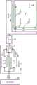
在实施例中,通过数据处理器400接收来自系统驱动器500的数据输出的第一数据矩阵401并在时间t0处将第一数据矩阵401直接保存至数据缓冲器430。可选地,第一数据矩阵401包括与设计用于在显示面板显示一帧图像的数据矩阵中的原始多列数据相同的多列数据。在实施例中,第一数据矩阵401还由第一移位寄存器410接收。在第一移位寄存器410中处理第一数据矩阵401中的每列数据以产生第二数据矩阵402,并且在时间t1处将第二数据矩阵402保存至数据缓冲器430。这里,时间t1不同于时间t0。时间t0和t1可以设置为t0在t1之前的顺序时序(sequential timing order)或反之亦然。可选地,第二数据矩阵402中的每列数据与在第一方向上移位了+m列的第一数据矩阵401中的对应列数据相同。可选地,m是小于10的整数。例如,m=1,即,对应于向右或向前移位一列,如图2A所示。第二数据矩阵402实质上是向前移位1列的第一数据矩阵401。具体而言,第二数据矩阵的第二列是从第一数据矩阵的第一列移位而来。第二数据矩阵的第三列是从第一数据矩阵的第二列移位而来。进一步地,第二数据矩阵的第k列是从第一数据矩阵的第(k-1)列移位而来。而第二数据矩阵的第一列重复为与第一数据矩阵的第一列相同。In an embodiment, the
可选地,可以通过在数据处理器400中处理第一数据矩阵401以使得第二数据矩阵402的每行与在第一方向上移位了+i行的第一数据矩阵401的对应行相同,来产生第二数据矩阵402。可选地,i是小于10的整数。例如,i=1对应于向下移位一行,如图2B所示。具体而言,第二数据矩阵的第二行是从第一数据矩阵的第一行移位而来。第二数据矩阵的第三行是从第一数据矩阵的第二行移位而来。进一步地,第二数据矩阵的第l行是从第一数据矩阵的第(l-1)行移位而来。而第二数据矩阵的第一行重复为与第一数据矩阵的第一行相同。Optionally, by processing the
此外,在实施例中,第一数据矩阵还由第二移位寄存器420接收。在第二移位寄存器420中处理第一数据矩阵401中的每列数据以产生第三数据矩阵403,并且在时间t2处将第三数据矩阵403保存至数据缓冲器430。这里,时间t2不同于t0并且也不同于t1。时间t0、t1和t2可以按任何顺序时序。在具体实施例中,在用于显示设备的从系统驱动器500至数据处理器400的整个数据输出处理中,t0、t1和t2的时序是固定顺序时序(无论该时序是什么时序)。可选地,第三数据矩阵403中的每列数据与在第二方向上移位了-n列的第一数据矩阵401中的对应列数据相同。可选地,n是小于10的整数。例如,n=1,即,对应于向左或向后移位一列,如图2A所示。第三数据矩阵403实质上是向后移位1列的第一数据矩阵401。具体而言,第三数据矩阵的第一列是从第一数据矩阵的第二列移位而来。第三数据矩阵的第二列是从第一数据矩阵的第三列移位而来。进一步地,第三数据矩阵的倒数第二列(第(k-1)列)是从第一数据矩阵的第k列移位而来。而第三数据矩阵的最后的第k列重复为与第一数据矩阵的最后一列相同。Furthermore, in an embodiment, the first data matrix is also received by the
可选地,可以通过在数据处理器400中处理第一数据矩阵401以使得第三数据矩阵403的每行与在第二方向上移位了-j行的第一数据矩阵401的对应行相同,来产生第三数据矩阵403。可选地,j是小于10的整数。例如,j=1对应于向上移位一行,如图2B所示。具体而言,第三数据矩阵的第一行是从第一数据矩阵的第二行移位而来。第三数据矩阵的第二行是从第一数据矩阵的第三行移位而来。进一步地,第三数据矩阵的倒数第二行(第(l-1)行)是从第一数据矩阵的第l行移位而来。而第三数据矩阵的最后的第l行重复为与第一数据矩阵的最后一行相同。Optionally, by processing the
返回参照图1,显示设备还包括耦接在数据处理器400和驱动器电路200之间的接口连接器300。可选地,接口连接器300按MIPI显示串行接口(MIPI DSI)协议配置,但也可以采用其他类型的数据通信接口架构。可选地,接口连接器300由数字使能信号EN使能以能够按特定通信方案从数据缓冲器430向驱动器电路200传送数据。Referring back to FIG. 1 , the display device further includes an
在实施例中,以通信方案配置接口连接器300以分别在用于显示一帧图像的单位时间的至少时分时段T0、T1、T2内,基于以与同t0、t1、t2相关联的固定顺序时序相同的顺序提供的定时信号控制第一数据矩阵、第二数据矩阵、第三数据矩阵从数据缓冲器430输出。In an embodiment, the communication scheme is used to configure the
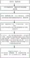
图3是根据本公开的实施例的用于使能接口连接器以发送时分数据的信号的时序图。例如,显示一帧图像的单位时间划分为至少三个时分时段T0、T1和T2。在一个时分时段T0中,定时信号MIPI(T0)提供为具有T0的脉宽的正电压脉冲,以使能接口连接器300打开数据处理器400中的数据缓冲器430与驱动器电路200之间的通信通道。3 is a timing diagram of signals for enabling an interface connector to send time-division data according to an embodiment of the disclosure. For example, the unit time for displaying one frame of image is divided into at least three time-division periods T0, T1 and T2. In a time-division period T0, the timing signal MIPI(T0) is provided as a positive voltage pulse having a pulse width of T0 to enable the
类似地,在另一时分时段T1中,提供另一定时信号MIPI(T1)以使能接口连接器300。在另一时分时段T2中,提供另一定时信号MIPI(T2)以使能接口连接器300。T0、T1和T2是在时间上不重叠的不同时段。T0、T1和T2之和不大于由显示刷新率确定的显示一帧图像的一个单位时间。虽然图3示出了T0开始、T1随后、T2再后的时间上的顺序,但是该时序也可以按其他顺序组合来排列,比如:T0、T2和T1;或者T1、T0和T2;或者T1、T2和T0;或者T2、T0和T1;或者T2、T1和T0。无论与T0、T1和T2相关联的定时信号的顺序是怎样的,其限制为与同t0、t1和t2相关联的固定顺序相同的顺序。换句话说,数据缓冲器430和接口连接器300的组合同步,以建立先进先出的数据输出方案。如果首先将第一数据矩阵401保存至数据缓冲器430中,则经由接口连接器300将第一数据矩阵401首先输出至驱动器电路200。如果将第二数据矩阵402保存至数据缓冲器430中(以擦除第一数据矩阵401),则经由接口连接器300将第二数据矩阵402随后输出至驱动器电路200。最后将第三数据矩阵403保存至数据缓冲器430中,也就最后经由接口连接器300将其输出至驱动器电路200。如果第一数据矩阵401、第二数据矩阵402和第三数据矩阵403以不同顺序相继保存至数据缓冲器中,则这三个数据矩阵将以所述不同顺序通过接口控制器输出至驱动器电路200。Similarly, another timing signal MIPI( T1 ) is provided to enable the
总之,由于分别在显示一帧图像的单位时间的至少三个时分时段中通过驱动器电路200使用至少三个时分输出数据来驱动显示面板100(参照图1),可以针对显示面板上所显示图像有效实现动态图像移位。在具体实施例中,参照图1,在每个时分时段(例如,T0、T1或者T2之一),驱动器电路200配置为产生控制信号以扫描显示面板100的一行,从而将对应数据矩阵(例如,数据矩阵401、402、403之一)的一行以这些数据被保存至数据缓冲器的相同时序从数据缓冲器加载至对应子像素行。从第一行至最后一行以相同时序持续执行该步骤。随着扫描信号一行接一行地扫过全部扫描线221,显示面板100在用于显示一帧图像的单位时间中基于时分数据显示图像帧。再一次地,显示面板以相同时序使用时分数据持续执行相同显示方案,以一帧一帧地显示图像。该显示方案实质上在人的视觉印象中增强了显示分辨率。其还有助于弥补显示面板中子像素之间的(例如,由于黑矩阵导致的)物理间隙。In a word, since at least three time-division output data are used to drive the display panel 100 (refer to FIG. 1 ) by the driver circuit 200 in at least three time-division periods of the unit time for displaying one frame of image, it is possible to efficiently display images on the display panel. Realize dynamic image shifting. In a specific embodiment, referring to FIG. 1 , in each time-division period (for example, one of T0, T1 or T2), the driver circuit 200 is configured to generate a control signal to scan a row of the display panel 100, so that the corresponding data matrix (for example, , one of the
参照图3,在实施例中,接口连接器300还配置为在每两个顺序定时信号之间的间隙时间T中停止输出。在通过定时信号MIPI(T0)使能而在时段T0中输出第一数据矩阵401之后,在间隙时间T内暂时停止输出。随后,提供另一定时信号MIPI(T1),其上升沿从上一定时信号MIPI(T0)的下降沿延迟了间隙时间T。引入间隙时间T以提供显示面板(假定该显示面板为LCD显示面板)中液晶层的关闭时间,从而消除分别在两个顺序时分时段中使用两个数据矩阵显示图像导致的混叠和曳尾效应。可以基于显示面板100中使用的特定液晶层的像素响应时间Tr来选择间隙时间T的值。像素响应指的是响应于电场改变的液晶分子旋转,该电场改变由与显示面板100中的液晶层相关联的对应的子像素电路基于通过驱动器电路200经由接口连接器300从数据缓冲器430接收到的两个随后的数据矩阵的变化而引起。时分时段T0、T1、T2中的任一个必须不小于Tr。时段T0、时段T1和时段T2以及至少两个间隙时间2T之和不大于显示一帧图像的单位时间。例如,液晶分子的像素响应时间Tr等于4ms。则T0、T1、或T2的最小时段为4ms。如果将显示一帧图像的单位时间划分为三个时分时段,则(基于全部三组数据的)总显示时间至少为12ms。如果显示面板的刷新率为60Hz,则显示一帧图像的单位时间为16.6ms。对于三个时分时段,需要至少两个间隙时间,因此间隙时间T将设为不大于2.3ms。对于具有像素响应时间更快(即,Tr更小)的液晶层的LCD显示面板而言,基于每个时分输出数据显示图像的最小时段可以更小,使得可以用于提供更高刷新率的应用。Referring to FIG. 3 , in an embodiment, the
在另一个实施例中,对于基于有机发光二极管(OLED)子像素的显示面板100或者使用有源发光子像素的其它面板而言,OLED的像素响应时间实质上可忽略。因此,时分时段可以选择为实质上没有下限,使得时分输出数据非常适于在高刷新率(比如240Hz或更高)显示设备上显示高质量、非常平滑且动态的图像。In another embodiment, for a display panel 100 based on organic light emitting diode (OLED) sub-pixels or other panels using active light-emitting sub-pixels, the pixel response time of the OLED is substantially negligible. Thus, the time-division period can be chosen with virtually no lower limit, making the time-division output data well suited for displaying high quality, very smooth and dynamic images on high refresh rate (eg 240Hz or higher) display devices.
另一方面,本公开提供了一种显示设备,包括本文所述的显示驱动电路,其与显示面板相耦接,实质上如图1所示。显示面板配置为利用从显示驱动电路传递的时分数据显示每帧图像。例如,时分数据在第一时段T0中提供为第一数据矩阵,在第二时段T1中提供为第二数据矩阵,并且在第三时段T2中提供为第三数据矩阵,其中T0、T1和T2是用于显示一帧图像的单位时间的时分时段。在实施例中,利用分别在T0、T1、或T2中的第一数据矩阵、第二数据矩阵、或第三数据矩阵在显示面板上显示图像的时序保持为与显示驱动电路产生这些数据矩阵并将其保存至数据缓冲器的顺序时序相同。In another aspect, the present disclosure provides a display device, including the display driving circuit described herein, coupled to a display panel, substantially as shown in FIG. 1 . The display panel is configured to display each frame of image using time-division data transferred from the display driving circuit. For example, time-division data is provided as a first data matrix in a first period T0, as a second data matrix in a second period T1, and as a third data matrix in a third period T2, wherein T0, T1 and T2 It is a time-division period of unit time for displaying one frame of image. In an embodiment, the timing of displaying images on the display panel using the first data matrix, the second data matrix, or the third data matrix in T0, T1, or T2, respectively, is maintained to be consistent with the generation of these data matrices by the display driving circuit and The sequence timing of saving it to the data buffer is the same.
另一方面,本公开提供了一种利用时分图像数据显示一帧图像的方法。图4示出了根据本公开的实施例的利用顺序地输出至显示设备的时分图像数据显示一帧图像的方法的流程图。参照图4,所述方法包括步骤:接收从显示设备的系统驱动器至常规驱动器集成电路(驱动器IC)前的数据处理器或预处理器的第一数据矩阵。数据处理器至少包括数据缓冲器、第一移位寄存器和第二移位寄存器。In another aspect, the present disclosure provides a method of displaying a frame of image using time-division image data. FIG. 4 shows a flowchart of a method for displaying a frame of image using time-division image data sequentially output to a display device according to an embodiment of the present disclosure. Referring to FIG. 4, the method includes the step of receiving a first data matrix from a system driver of a display device to a data processor or pre-processor in front of a conventional driver integrated circuit (driver IC). The data processor includes at least a data buffer, a first shift register and a second shift register.
可选地,参照图4,所述方法还包括步骤:在时间t0处将第一数据矩阵存储至数据缓冲器。可选地,所述方法还包括:将第一数据矩阵在第一方向上移位m列以获得在不同于t0的时间t1处存储至数据缓冲器中的第二数据矩阵。可选地,所述方法还包括:将第一数据矩阵在与第一方向相反的第二方向上移位-n列以获得在时间t2处存储至数据缓冲器中的第三数据矩阵。时间t2不同于t0或t1,但是在与t0、t1和t2相关联的固定顺序时序中固定。可选地,t0在时间上位于t1、t2之前。可选地,t1在时间上位于t0、t2之前。可选地,t2在时间上位于t1、t0之前。但是,数据缓冲器配置为在固定顺序时序中仅暂时保留第一数据矩阵、第二数据矩阵、第三数据矩阵中的一组数据。Optionally, referring to FIG. 4 , the method further includes the step of: storing the first data matrix into the data buffer at time t0. Optionally, the method further includes: shifting the first data matrix by m columns in a first direction to obtain a second data matrix stored in the data buffer at a time t1 different from t0. Optionally, the method further includes: shifting the first data matrix by -n columns in a second direction opposite to the first direction to obtain a third data matrix stored in the data buffer at time t2. Time t2 is different from t0 or t1, but is fixed in a fixed sequential timing associated with t0, t1 and t2. Optionally, t0 is located before t1 and t2 in time. Optionally, t1 is located before t0 and t2 in time. Optionally, t2 is located before t1 and t0 in time. However, the data buffer is configured to only temporarily retain a set of data in the first data matrix, the second data matrix, and the third data matrix in a fixed sequential timing.
可选地,所述方法包括步骤:以与同t0、t1和t2相关联的固定顺序时序相同的顺序,在时段T0中将第一数据矩阵从数据缓冲器输出至显示面板的驱动器电路,在时段T1中将第二数据矩阵从数据缓冲器输出至显示面板的驱动器电路,以及在时段T2中将第三数据矩阵从数据缓冲器输出至显示面板的驱动器电路。时段T0、时段T1和时段T2是用于显示一帧图像的一个单位时间的至少三个时分时段,所述单位时间取决于设计用于显示设备的显示刷新率。在实施例中,所述方法还包括:在时段T0中使用第一数据矩阵、在时段T1中使用第二数据矩阵和在时段T2中使用第三数据矩阵,基于显示刷新率显示一帧图像。在实施例中,驱动器IC接收每组数据(第一数据矩阵、第二数据矩阵、或第三数据矩阵),并且产生控制信号以扫过显示面板中的所有行子像素电路,以在所述至少三个时分时段T0、T1和T2中的对应一个加载对应的数据矩阵。Optionally, the method comprises the steps of: outputting the first data matrix from the data buffer to the driver circuit of the display panel during the period T0 in the same order as the fixed sequential timing associated with t0, t1 and t2, at The second data matrix is output from the data buffer to the driver circuit of the display panel in the period T1, and the third data matrix is output from the data buffer to the driver circuit of the display panel in the period T2. Period T0, period T1 and period T2 are at least three time-division periods for displaying one frame of image for a unit time depending on a display refresh rate designed for a display device. In an embodiment, the method further includes: using the first data matrix in the period T0, using the second data matrix in the period T1, and using the third data matrix in the period T2, to display a frame of image based on the display refresh rate. In an embodiment, the driver IC receives each set of data (the first data matrix, the second data matrix, or the third data matrix), and generates control signals to sweep all rows of sub-pixel circuits in the display panel to A corresponding data matrix is loaded in a corresponding one of at least three time-division periods T0, T1 and T2.
在实施例中,将第一数据矩阵在第一方向上移位m列的步骤包括:使第一数据矩阵由移位寄存器处理,所述移位寄存器配置为将第一数据矩阵中的对应第k列数据分配至第二数据矩阵中的第(k-m)列数据并且保持所有的最后m个列数据重复作为第一数据矩阵中的最后一列数据。具体地,m是小于10的整数。在一个示例中,m=1,第一数据矩阵中的每列向前移位一列以获得第二数据矩阵。可以以时分方式将第二数据矩阵和第一数据矩阵从驱动器IC传递至显示面板,以使得显示面板可以以增强视觉分辨率显示动态但平滑移位的图像数据。In an embodiment, the step of shifting the first data matrix by m columns in the first direction comprises: causing the first data matrix to be processed by a shift register configured to shift the corresponding first data matrix in the first data matrix K columns of data are allocated to the (k-m)th column of data in the second data matrix and all the last m columns of data are kept repeated as the last column of data in the first data matrix. Specifically, m is an integer less than 10. In one example, m=1, each column in the first data matrix is shifted forward by one column to obtain the second data matrix. The second data matrix and the first data matrix can be transferred from the driver IC to the display panel in a time-divisional manner so that the display panel can display dynamically but smoothly shifted image data with enhanced visual resolution.
在实施例中,将第一数据矩阵在第二方向上移位-n列的步骤包括:使第一数据矩阵由移位寄存器处理,所述移位寄存器配置为将第一数据矩阵中的对应第k列数据分配至第三数据矩阵中的第(k+n)列数据并且保持所有的最初n个列数据重复作为第一数据矩阵中的第一列数据。具体地,n是小于10的整数。在一个示例中,n=1,第一数据矩阵中的每列向后移位一列以获得第三数据矩阵。可以以时分方式将第三数据矩阵、第二数据矩阵和第一数据矩阵从驱动器IC传递至显示面板,以使得显示面板可以以增强视觉分辨率显示动态但平滑移位的图像数据。In an embodiment, the step of shifting the first data matrix by -n columns in the second direction comprises: causing the first data matrix to be processed by a shift register configured to shift corresponding The k-th column of data is assigned to the (k+n)-th column of data in the third data matrix and all the first n columns of data are kept repeatedly as the first column of data in the first data matrix. Specifically, n is an integer less than 10. In one example, n=1, each column in the first data matrix is shifted backward by one column to obtain the third data matrix. The third data matrix, the second data matrix and the first data matrix may be transferred from the driver IC to the display panel in a time-divisional manner so that the display panel can display dynamically but smoothly shifted image data with enhanced visual resolution.
在实施例中,所述方法包括:将时段T0、T1和T2中的任一个设置为不小于与显示面板相关联的像素响应时间。In an embodiment, the method includes setting any one of the periods T0, T1 and T2 to be not less than a pixel response time associated with the display panel.
在实施例中,输出步骤还包括在任意两个顺序定时信号之间的间隙时间T中停止。基于至少T0、T1、T2以及两个间隙时间2×T之和不大于取决于显示刷新率的用于显示一帧图像的单位时间,来确定间隙时间T。对于LCD显示器,每个时分时段至少被设置为与显示面板的液晶层相关联的最小像素响应时间。对于OLED显示器,由于每个子像素电路包括有源发光器件,其像素响应时间实质上可忽略,因此不存在针对时分时段设置的理论下限,并且所述显示方法可以在具有超高刷新率的显示设备中实现。In an embodiment, the step of outputting further comprises stopping in an interstitial time T between any two sequential timing signals. The gap time T is determined based on at least T0, T1, T2 and the sum of the two
出于示意和描述目的已示出对本发明实施例的上述描述。其并非旨在穷举或将本发明限制为所公开的确切形式或示例性实施例。因此,上述描述应当被认为是示意性的而非限制性的。显然,许多修改和变形对于本领域技术人员而言将是显而易见的。选择和描述这些实施例是为了解释本发明的原理和其最佳方式的实际应用,从而使得本领域技术人员能够理解本发明适用于特定用途或所构思的实施方式的各种实施例及各种变型。本发明的范围旨在由所附权利要求及其等同形式限定,其中除非另有说明,否则所有术语以其最宽的合理意义解释。因此,术语“发明”、“本发明”等不一定将权利范围限制为具体实施例,并且对本发明示例性实施例的参考不隐含对本发明的限制,并且不应推断出这种限制。本发明仅由随附权利要求的精神和范围限定。此外,这些权利要求可涉及使用跟随有名词或元素的“第一”、“第二”等术语。这种术语应当理解为一种命名方式而非意在对由这种命名方式修饰的元素的数量进行限制,除非给出具体数量。所描述的任何优点和益处不一定适用于本发明的全部实施例。应当认识到的是,本领域技术人员在不脱离随附权利要求所限定的本发明的范围的情况下可以对所描述的实施例进行变化。此外,本公开中没有元件和组件是意在贡献给公众的,无论该元件或组件是否明确地记载在随附权利要求中。The foregoing descriptions of embodiments of the invention have been presented for purposes of illustration and description. It is not intended to be exhaustive or to limit the invention to the precise forms or exemplary embodiments disclosed. Accordingly, the foregoing description should be considered as illustrative rather than restrictive. Obviously, many modifications and variations will be apparent to those skilled in the art. The embodiments were chosen and described in order to explain the principles of the invention and the best mode practical application thereof, thereby enabling others skilled in the art to understand various embodiments and various embodiments of the invention as suited to a particular use or contemplated implementation. transform. The scope of the invention is intended to be defined by the appended claims and their equivalents, wherein all terms are to be interpreted in their broadest reasonable sense unless otherwise indicated. Thus, the terms "invention," "present invention," etc. do not necessarily limit the scope of claims to the specific embodiments, and references to exemplary embodiments of the invention do not imply, and should not be inferred, limitations of the invention. The present invention is limited only by the spirit and scope of the appended claims. Furthermore, these claims may involve the use of the terms "first", "second", etc. followed by a noun or element. Such terms should be understood as a nomenclature and are not intended to be limiting of the number of elements modified by such nomenclature, unless a specific number is given. Any advantages and benefits described do not necessarily apply to all embodiments of the invention. It should be appreciated that variations may be made in the described embodiments by those skilled in the art without departing from the scope of the invention as defined in the appended claims. Furthermore, no element or component in the present disclosure is intended to be dedicated to the public regardless of whether the element or component is explicitly recited in the accompanying claims.
Claims (18)
Translated fromChineseApplications Claiming Priority (1)
| Application Number | Priority Date | Filing Date | Title |
|---|---|---|---|
| PCT/CN2019/076859WO2020177053A1 (en) | 2019-03-04 | 2019-03-04 | Display-driving circuit, display apparatus, and display method based on time-division data output |
Publications (2)
| Publication Number | Publication Date |
|---|---|
| CN110800038A CN110800038A (en) | 2020-02-14 |
| CN110800038Btrue CN110800038B (en) | 2023-06-13 |
Family
ID=69448543
Family Applications (1)
| Application Number | Title | Priority Date | Filing Date |
|---|---|---|---|
| CN201980000215.4AActiveCN110800038B (en) | 2019-03-04 | 2019-03-04 | Display driving circuit, display device and display method based on time division data output |
Country Status (3)
| Country | Link |
|---|---|
| US (1) | US11238819B2 (en) |
| CN (1) | CN110800038B (en) |
| WO (1) | WO2020177053A1 (en) |
Families Citing this family (4)
| Publication number | Priority date | Publication date | Assignee | Title |
|---|---|---|---|---|
| TWI762956B (en)* | 2020-06-17 | 2022-05-01 | 瑞昱半導體股份有限公司 | Method for processing a static pattern in an image |
| CN112667191A (en)* | 2021-01-19 | 2021-04-16 | 青岛海尔科技有限公司 | Display method and device, storage medium and electronic device |
| EP4528698A3 (en)* | 2021-09-18 | 2025-05-21 | Jade Bird Display (Shanghai) Limited | Micro display back plane system and pixel driver controller |
| CN119718237A (en)* | 2023-09-28 | 2025-03-28 | 华为技术有限公司 | Image display method, device, near-eye display device and readable storage medium |
Citations (5)
| Publication number | Priority date | Publication date | Assignee | Title |
|---|---|---|---|---|
| CN1744166A (en)* | 2001-07-31 | 2006-03-08 | 佳能株式会社 | Scanning circuit and image display device |
| JP2010220150A (en)* | 2009-03-19 | 2010-09-30 | Casio Computer Co Ltd | Projector, image projection control program, and image projecting method |
| CN103093722A (en)* | 2013-02-22 | 2013-05-08 | 厦门大学 | Four-color light-emitting diode (LED) display sub-pixel restructuring method |
| CN103247254A (en)* | 2012-02-10 | 2013-08-14 | 三星显示有限公司 | Display device and arranging method for image data thereof |
| CN108604436A (en)* | 2016-01-13 | 2018-09-28 | 深圳云英谷科技有限公司 | Device and method for pixel data rearrangement |
Family Cites Families (22)
| Publication number | Priority date | Publication date | Assignee | Title |
|---|---|---|---|---|
| US5230064A (en)* | 1991-03-11 | 1993-07-20 | Industrial Technology Research Institute | High resolution graphic display organization |
| US5799174A (en)* | 1994-12-08 | 1998-08-25 | The Regents Of The University Of California | Staggered striping in multimedia information systems |
| GB2333174A (en)* | 1998-01-09 | 1999-07-14 | Sharp Kk | Data line driver for an active matrix display |
| TW493152B (en)* | 1999-12-24 | 2002-07-01 | Semiconductor Energy Lab | Electronic device |
| CN1184819C (en) | 2002-04-18 | 2005-01-12 | 华为技术有限公司 | Picture smoothly displaying method |
| TWI231465B (en)* | 2003-11-14 | 2005-04-21 | Au Optronics Corp | Driving circuit for liquid crystal display and liquid crystal display using the driving circuit |
| JP2005208413A (en)* | 2004-01-23 | 2005-08-04 | Ricoh Co Ltd | Image processing apparatus and image display apparatus |
| KR20060086021A (en)* | 2005-01-25 | 2006-07-31 | 삼성전자주식회사 | Display device and driving apparatus method of display device |
| TWI357037B (en) | 2006-04-28 | 2012-01-21 | Himax Tech Inc | Flat display and driving method thereof |
| JP5343714B2 (en)* | 2009-06-05 | 2013-11-13 | ソニー株式会社 | Video processing device, display device, and display system |
| TWI436321B (en)* | 2009-06-25 | 2014-05-01 | Innolux Corp | Image display system |
| KR101895530B1 (en)* | 2012-02-10 | 2018-09-06 | 삼성디스플레이 주식회사 | Display device and driving method of the same |
| KR102012023B1 (en)* | 2012-02-10 | 2019-08-20 | 삼성디스플레이 주식회사 | Display device and memory arranging method for image data thereof |
| KR101903789B1 (en) | 2012-02-17 | 2018-10-02 | 리쿠아비스타 비.브이. | Eletrowetting display device and driving method thereof |
| JP6115056B2 (en)* | 2012-09-18 | 2017-04-19 | 株式会社Jvcケンウッド | Liquid crystal display |
| JP6320679B2 (en)* | 2013-03-22 | 2018-05-09 | セイコーエプソン株式会社 | LATCH CIRCUIT FOR DISPLAY DEVICE, DISPLAY DEVICE, AND ELECTRONIC DEVICE |
| US9582237B2 (en)* | 2013-12-31 | 2017-02-28 | Ultravision Technologies, Llc | Modular display panels with different pitches |
| US9892669B2 (en)* | 2014-03-18 | 2018-02-13 | Nvidia Corporation | Superresolution display using cascaded panels |
| US20180293949A1 (en)* | 2015-10-19 | 2018-10-11 | Sharp Kabushiki Kaisha | Data processing device connected with display device and control method of display device |
| CN107016977B (en)* | 2017-06-15 | 2020-05-05 | 武汉华星光电技术有限公司 | Data driving circuit and display panel |
| KR102360412B1 (en)* | 2017-08-25 | 2022-02-09 | 엘지디스플레이 주식회사 | Image generation method and display device using the same |
| CN109194944B (en)* | 2018-10-29 | 2020-06-09 | 京东方科技集团股份有限公司 | Image processing method, device and system, and display device |
- 2019
- 2019-03-04CNCN201980000215.4Apatent/CN110800038B/enactiveActive
- 2019-03-04WOPCT/CN2019/076859patent/WO2020177053A1/ennot_activeCeased
- 2019-03-04USUS16/638,933patent/US11238819B2/enactiveActive
Patent Citations (5)
| Publication number | Priority date | Publication date | Assignee | Title |
|---|---|---|---|---|
| CN1744166A (en)* | 2001-07-31 | 2006-03-08 | 佳能株式会社 | Scanning circuit and image display device |
| JP2010220150A (en)* | 2009-03-19 | 2010-09-30 | Casio Computer Co Ltd | Projector, image projection control program, and image projecting method |
| CN103247254A (en)* | 2012-02-10 | 2013-08-14 | 三星显示有限公司 | Display device and arranging method for image data thereof |
| CN103093722A (en)* | 2013-02-22 | 2013-05-08 | 厦门大学 | Four-color light-emitting diode (LED) display sub-pixel restructuring method |
| CN108604436A (en)* | 2016-01-13 | 2018-09-28 | 深圳云英谷科技有限公司 | Device and method for pixel data rearrangement |
Also Published As
| Publication number | Publication date |
|---|---|
| WO2020177053A1 (en) | 2020-09-10 |
| US11238819B2 (en) | 2022-02-01 |
| CN110800038A (en) | 2020-02-14 |
| US20210233482A1 (en) | 2021-07-29 |
Similar Documents
| Publication | Publication Date | Title |
|---|---|---|
| CN101248481B (en) | Display device, display method, display monitor, and television set | |
| US11380271B2 (en) | Backlight driving method, display driving method, drive device and display device | |
| CN110800038B (en) | Display driving circuit, display device and display method based on time division data output | |
| EP2306441B1 (en) | Scan-type display device control circuit | |
| US9111506B2 (en) | Display device having a gate driver responsive to multiple scan start signals | |
| CN110517633A (en) | Display panel, display device and driving method | |
| US10431144B2 (en) | Scan circuit unit, driving method thereof, gate drive circuit, and display apparatus | |
| CN104157249A (en) | Grid driving method and driving device of display panel and display device | |
| WO2005116971A1 (en) | Active matrix display device | |
| JP2006267999A (en) | Drive circuit chip and display device | |
| US11935459B2 (en) | Display apparatus | |
| CN103262546A (en) | Display device and driving method thereof | |
| CN108269549B (en) | Silicon-based micro-display based on digital pixel drive | |
| CN117456939A (en) | Control method and equipment for backlight unit | |
| CN111916018A (en) | Display panel and driving method thereof | |
| WO2023202507A1 (en) | Gate driving control method and system, display driving system, and display apparatus | |
| JP2007212571A (en) | Video display device | |
| WO2022021529A1 (en) | Backlight processing system, apparatus and method, backlight driver, and storage medium | |
| CN112785968B (en) | Control device, display device and operation method thereof | |
| JP7517777B2 (en) | Display device and driving method thereof | |
| TWI703541B (en) | Source driver module, display device and method for driving a display panel | |
| CN111312142B (en) | Driving method and device for improving image display quality | |
| JP7620065B2 (en) | Variable duty ratio display scanning method and system - Patents.com | |
| JP2019020447A (en) | Method for driving display and display | |
| JP2006119447A (en) | Display panel control circuit |
Legal Events
| Date | Code | Title | Description |
|---|---|---|---|
| PB01 | Publication | ||
| PB01 | Publication | ||
| SE01 | Entry into force of request for substantive examination | ||
| SE01 | Entry into force of request for substantive examination | ||
| GR01 | Patent grant | ||
| GR01 | Patent grant |