CN110798155A - A power amplifier AM-PM distortion correction circuit and method - Google Patents
A power amplifier AM-PM distortion correction circuit and methodDownload PDFInfo
- Publication number
- CN110798155A CN110798155ACN201911038882.XACN201911038882ACN110798155ACN 110798155 ACN110798155 ACN 110798155ACN 201911038882 ACN201911038882 ACN 201911038882ACN 110798155 ACN110798155 ACN 110798155A
- Authority
- CN
- China
- Prior art keywords
- signal
- phase
- electrically connected
- capacitor array
- multiplexer
- Prior art date
- Legal status (The legal status is an assumption and is not a legal conclusion. Google has not performed a legal analysis and makes no representation as to the accuracy of the status listed.)
- Pending
Links
- 238000012937correctionMethods0.000titleclaimsabstractdescription24
- 238000000034methodMethods0.000titleclaimsabstractdescription23
- 239000003990capacitorSubstances0.000claimsabstractdescription86
- 238000012545processingMethods0.000claimsdescription3
- 230000000694effectsEffects0.000abstractdescription4
- 230000010363phase shiftEffects0.000abstractdescription3
- 238000011105stabilizationMethods0.000abstractdescription3
- 238000010586diagramMethods0.000description6
- 238000005516engineering processMethods0.000description5
- 238000013461designMethods0.000description2
- 238000005070samplingMethods0.000description2
- 238000007792additionMethods0.000description1
- 238000003491arrayMethods0.000description1
- 230000003993interactionEffects0.000description1
- 238000012986modificationMethods0.000description1
- 230000004048modificationEffects0.000description1
- 230000003071parasitic effectEffects0.000description1
- 238000006467substitution reactionMethods0.000description1
Images


Classifications
- H—ELECTRICITY
- H03—ELECTRONIC CIRCUITRY
- H03F—AMPLIFIERS
- H03F1/00—Details of amplifiers with only discharge tubes, only semiconductor devices or only unspecified devices as amplifying elements
- H03F1/32—Modifications of amplifiers to reduce non-linear distortion
- H—ELECTRICITY
- H03—ELECTRONIC CIRCUITRY
- H03F—AMPLIFIERS
- H03F1/00—Details of amplifiers with only discharge tubes, only semiconductor devices or only unspecified devices as amplifying elements
- H03F1/30—Modifications of amplifiers to reduce influence of variations of temperature or supply voltage or other physical parameters
- H—ELECTRICITY
- H03—ELECTRONIC CIRCUITRY
- H03F—AMPLIFIERS
- H03F1/00—Details of amplifiers with only discharge tubes, only semiconductor devices or only unspecified devices as amplifying elements
- H03F1/34—Negative-feedback-circuit arrangements with or without positive feedback
- H—ELECTRICITY
- H03—ELECTRONIC CIRCUITRY
- H03F—AMPLIFIERS
- H03F3/00—Amplifiers with only discharge tubes or only semiconductor devices as amplifying elements
- H03F3/20—Power amplifiers, e.g. Class B amplifiers, Class C amplifiers
- H03F3/21—Power amplifiers, e.g. Class B amplifiers, Class C amplifiers with semiconductor devices only
- H03F3/211—Power amplifiers, e.g. Class B amplifiers, Class C amplifiers with semiconductor devices only using a combination of several amplifiers
Landscapes
- Engineering & Computer Science (AREA)
- Power Engineering (AREA)
- Physics & Mathematics (AREA)
- Nonlinear Science (AREA)
- Amplifiers (AREA)
Abstract
Translated fromChinese
Description
Translated fromChinese技术领域technical field
本申请涉及功率放大器技术领域,具体涉及一种功率放大器AM-PM失真校正电路及方法。The present application relates to the technical field of power amplifiers, and in particular, to a power amplifier AM-PM distortion correction circuit and method.
背景技术Background technique
在数字功率放大器(DigitalPowerAmplifier,DPA)中,由于末级开关管的非线性和寄生参数会导致输出信号的相位受输出幅度影响。输出相位随输出幅度影响会导致调制信号的质量恶化,误差向量幅度增加。为了解决非线性以及输出幅度和相位之间的相互影响,需要引入数字预失真技术。数字预失真技术会增加系统的复杂性,需要DPA具有高线性度避免数字预失真的需要。In a digital power amplifier (Digital Power Amplifier, DPA), the phase of the output signal is affected by the output amplitude due to the nonlinearity and parasitic parameters of the final switch. The effect of the output phase on the output amplitude causes the quality of the modulated signal to deteriorate and the magnitude of the error vector to increase. To address the nonlinearity and the interaction between output amplitude and phase, digital predistortion techniques need to be introduced. Digital pre-distortion technology will increase the complexity of the system, requiring DPA to have high linearity to avoid the need for digital pre-distortion.
现有技术中为了实现失真校正,为了实现对电路的补偿,有以下几种方案。如图1采用基于变压器的AM-PM补偿电路。如图1所示,变压器原边串联在驱动放大器的输入。输入信号幅度小时MSW不导通,变压器次边没有电流,原边电感量较大。输入信号幅度大时MSW导通,次边有电流,使得原边的电感量减小,驱动放大器输入相位提前,补偿了驱动和功率放大级在大幅度时的相位滞后。如图2增加P型变容二极管的方式。P型变容二极管的容值随输入信号功率变化,趋势与后级NMOS放大电路的趋势相反。补偿了后级NMOS放大电路输入电容随幅度的变化。避免因放大电路输入电容变化导致的AM-PM失真。如图3通过改变数字PA开关单元的结构。在上管(M3、M4)的源极和漏极之间并联电容,同时在单元关闭时降低上管栅极电压。使得PA的输出电容值在单元打开和关闭时保持不变。In the prior art, in order to realize distortion correction and to realize circuit compensation, there are the following schemes. As shown in Figure 1, a transformer-based AM-PM compensation circuit is used. As shown in Figure 1, the primary side of the transformer is connected in series with the input of the driver amplifier. When the input signal amplitude is small, MSW does not conduct, there is no current on the secondary side of the transformer, and the inductance of the primary side is large. When the amplitude of the input signal is large, the MSW is turned on, and there is current on the secondary side, which reduces the inductance of the primary side, and the input phase of the driver amplifier advances, compensating for the phase lag of the driver and power amplifier stages when the amplitude is large. As shown in Figure 2, the way of adding a P-type varactor diode. The capacitance value of the P-type varactor varies with the input signal power, and the trend is opposite to that of the subsequent NMOS amplifier circuit. The change of the input capacitance of the post-stage NMOS amplifying circuit with the amplitude is compensated. Avoid AM-PM distortion caused by changes in the input capacitance of the amplifier circuit. As shown in Figure 3, by changing the structure of the digital PA switch unit. Capacitors are connected in parallel between the source and drainof the upper transistors (M3, M4) , while reducing the upper transistor gate voltage when the cell is turned off. This makes the PA's output capacitance value unchanged when the unit is turned on and off.
但是现有技术使用无源电路,需要进行比较精确的设计,同时无源补偿电路的特性难以在宽频带内与PA的特性匹配,使得在宽带时补偿电路设计困难。技术一、二在PA输入增加电路根据输入幅度进行补偿,因此只适用于模拟PA。数字PA因输入幅度不变,无法使用此方法。技术三适用于数字PA,但因为在单元关断时需要降低栅极电压,使得栅极漏极之间的电压差增加,可靠性差。However, the prior art uses a passive circuit, which requires a relatively accurate design, and at the same time, the characteristics of the passive compensation circuit are difficult to match with the characteristics of the PA in a wide frequency band, which makes it difficult to design the compensation circuit in a wide frequency band. Techniques 1 and 2 add circuits to the PA input to compensate according to the input amplitude, so they are only applicable to analog PAs. Digital PAs cannot use this method because the input amplitude does not change. The third technique is suitable for digital PA, but because the gate voltage needs to be reduced when the cell is turned off, the voltage difference between the gate and the drain increases, and the reliability is poor.
发明内容SUMMARY OF THE INVENTION
本申请为了解决上述技术问题,提出了如下技术方案:In order to solve the above-mentioned technical problems, the present application proposes the following technical solutions:
第一方面,本申请实施例提供了一种功率放大器AM-PM失真校正电路,包括功率放大器PA,所述PA的第一信号输入端与校准移相器的信号输出端电连接,所述PA的信号输出端与鉴相器的第一信号输入端电连接,所述鉴相器的信号输出端与电容器阵列的第一信号输入端电连接,所述电容器阵列的信号输出端与所述校准移相器的第一信号输入端电连接,所述电容器阵列中设置有多组电容,不同电容对应不同的校准环路稳定电压。In a first aspect, an embodiment of the present application provides a power amplifier AM-PM distortion correction circuit, including a power amplifier PA, a first signal input end of the PA is electrically connected to a signal output end of a calibration phase shifter, the PA The signal output terminal of the phase detector is electrically connected to the first signal input terminal of the phase detector, the signal output terminal of the phase detector is electrically connected to the first signal input terminal of the capacitor array, and the signal output terminal of the capacitor array is electrically connected to the calibration The first signal input end of the phase shifter is electrically connected, and the capacitor array is provided with a plurality of groups of capacitors, and different capacitors correspond to different calibration loop stable voltages.
采用上述实现方式,通过切换电容阵列,可以实现在不同幅度时控制电压能够迅速切换到使PA的相移被完全补偿时的电压,实现前馈效果。避免了每次幅度切换时重新稳定引起的相位误差。鉴相器可以在宽频带工作,能够实现宽频带覆盖。同时,反馈电路能够补偿因温度等原因导致的相位缓慢变化。在模拟域上完成校准功能,数字部分辅助开关切换,避免了常规DPD中复杂的采样及计算电路,降低了系统的复杂度。With the above implementation manner, by switching the capacitor array, the control voltage can be rapidly switched to the voltage at which the phase shift of the PA is fully compensated at different amplitudes, thereby realizing the feedforward effect. Phase errors due to re-stabilization at each amplitude switch are avoided. The phase detector can work in a wide frequency band and can achieve wide frequency band coverage. At the same time, the feedback circuit can compensate for slow changes in phase due to temperature, etc. The calibration function is completed in the analog domain, and the digital part assists the switch switching, which avoids the complex sampling and calculation circuits in the conventional DPD, and reduces the complexity of the system.
结合第一方面,在第一方面第一种可能的实现方式中,所述鉴相器与所述电容器阵列之间设置有跨导放大器OTA,所述OTA的两端分别与所述鉴相器的信号输出端和所述电容器阵列的第一信号输入端电连接。With reference to the first aspect, in a first possible implementation manner of the first aspect, a transconductance amplifier OTA is arranged between the phase detector and the capacitor array, and two ends of the OTA are respectively connected to the phase detector. The signal output terminal of the capacitor array is electrically connected to the first signal input terminal of the capacitor array.
结合第一方面第一种可能的实现方式,在第一方面第二种可能的实现方式中,所述电容器阵列与所述校准移相器之间设置有缓冲放大器,所述缓冲放大器的两端分别与所述电容器阵列的信号输出端和所述校准移相器的第一信号输入端电连接。With reference to the first possible implementation manner of the first aspect, in a second possible implementation manner of the first aspect, a buffer amplifier is provided between the capacitor array and the calibration phase shifter, and both ends of the buffer amplifier are It is electrically connected to the signal output terminal of the capacitor array and the first signal input terminal of the calibration phase shifter, respectively.
结合第一方面第二种可能的实现方式,在第一方面第三种可能的实现方式中,所述PA的第二信号输入端和所述电容器阵列的第二信号输入端用于接收幅度控制码。With reference to the second possible implementation manner of the first aspect, in a third possible implementation manner of the first aspect, the second signal input terminal of the PA and the second signal input terminal of the capacitor array are used for receiving amplitude control code.
结合第一方面第三种可能的实现方式,在第一方面第四种可能的实现方式中,所述电容器阵列包括第一多路复用器、第二多路复用器和多个电容,多个所述电容独立设置,所述电容的第一端分别与所述第一多路复用器的第一端和所述第二多路复用器的第一端电连接,所述电容的第二端接地,所述第一多路复用器的第二端与所述OTA的信号输出端电连接,所述第二多路复用器的第二端与所述缓冲放大器的信号输入端电连接。With reference to the third possible implementation manner of the first aspect, in a fourth possible implementation manner of the first aspect, the capacitor array includes a first multiplexer, a second multiplexer and a plurality of capacitors, A plurality of the capacitors are independently arranged, the first ends of the capacitors are respectively electrically connected to the first end of the first multiplexer and the first end of the second multiplexer, and the capacitors The second end of the first multiplexer is grounded, the second end of the first multiplexer is electrically connected to the signal output end of the OTA, and the second end of the second multiplexer is connected to the signal of the buffer amplifier The input terminal is electrically connected.
结合第一方面第四种可能的实现方式,在第一方面第五种可能的实现方式中,所述第一多路复用器和所述第二多路复用器均与一译码器电连接,所述译码器用于向所述第一多路复用器和所述第二多路复用器输出选择信号。With reference to the fourth possible implementation manner of the first aspect, in the fifth possible implementation manner of the first aspect, the first multiplexer and the second multiplexer are both connected to a decoder electrically connected, and the decoder is configured to output a selection signal to the first multiplexer and the second multiplexer.
结合第一方面第五种可能的实现方式,在第一方面第六种可能的实现方式中,所述移相器的第二信号输入端与信号发生器电连接,所述移相器用于将所述信号发生器产生的调相信号进行相位处理后发送给所述PA。With reference to the fifth possible implementation manner of the first aspect, in the sixth possible implementation manner of the first aspect, the second signal input end of the phase shifter is electrically connected to the signal generator, and the phase shifter is used to The phase-modulated signal generated by the signal generator is subjected to phase processing and then sent to the PA.
结合第一方面第六种可能的实现方式,在第一方面第七种可能的实现方式中,所述鉴相器的第二信号输入端与所述信号发生器电连接,所述鉴相器用于比较所述PA的输入信号和所述输出信号的相位差。In combination with the sixth possible implementation manner of the first aspect, in the seventh possible implementation manner of the first aspect, the second signal input end of the phase detector is electrically connected to the signal generator, and the phase detector uses for comparing the phase difference between the input signal of the PA and the output signal.
第二方面,本申请实施例提供了一种功率放大器AM-PM失真校正方法,采用第一方面或第一方面任一实现方式所述的功率放大器AM-PM失真校正电路,所述方法包括:鉴相器比较PA的输出信号和输入信号的相位差;将所述相位差转换为电压信号输入到电容器阵列;所述电容器阵列输出电压控制校准移相器进行相位补偿。In a second aspect, an embodiment of the present application provides a power amplifier AM-PM distortion correction method, using the power amplifier AM-PM distortion correction circuit described in the first aspect or any implementation manner of the first aspect, and the method includes: The phase detector compares the phase difference between the output signal of the PA and the input signal; converts the phase difference into a voltage signal and inputs it to the capacitor array; the output voltage of the capacitor array controls the calibration phase shifter to perform phase compensation.
结合第二方面,在第二方面第一种可能的实现方式中,所述电容器阵列输出电压控制校准移相器进行相位补偿包括:不同的选择信号经译码器控制多路复用器选中不同的电容;第一多路复用器和第二多路复用器分别控制与跨导放大器和缓冲放大器之间的连接;反馈环路调整电容上的电压值直到输出与参考信号同相或存在固有的相位差。With reference to the second aspect, in a first possible implementation manner of the second aspect, the output voltage of the capacitor array controlling the calibration phase shifter to perform phase compensation includes: different selection signals are selected by the decoder to control the multiplexer to select different capacitors; the first and second multiplexers control the connections to the transconductance amplifier and buffer amplifier, respectively; the feedback loop adjusts the voltage across the capacitors until the output is in phase with the reference signal or there is an inherent phase difference.
附图说明Description of drawings
图1为传统技术中基于变压器的AM-PM补偿电路的结构示意图;1 is a schematic structural diagram of a transformer-based AM-PM compensation circuit in the conventional technology;
图2为传统技术中基于P型变容二极管的AM-PM补偿电路的结构示意图;2 is a schematic structural diagram of an AM-PM compensation circuit based on a P-type varactor diode in the conventional technology;
图3为传统技术中改变数字PA开关单元补偿电路的结构示意图;3 is a schematic structural diagram of a compensation circuit for changing a digital PA switch unit in the conventional technology;
图4为本申请实施例提供的一种功率放大器AM-PM失真校正电路的结构示意图;4 is a schematic structural diagram of a power amplifier AM-PM distortion correction circuit provided by an embodiment of the present application;
图5为本申请实施例提供的一种电容器阵列的结构示意图;FIG. 5 is a schematic structural diagram of a capacitor array provided by an embodiment of the present application;
图6为本申请实施例提供的一种功率放大器AM-PM失真校正方法的流程示意图。FIG. 6 is a schematic flowchart of a method for correcting AM-PM distortion of a power amplifier according to an embodiment of the present application.
具体实施方式Detailed ways
下面结合附图与具体实施方式对本方案进行阐述。The solution will be described below with reference to the accompanying drawings and specific embodiments.
图4为本申请实施例提供的一种功率放大器AM-PM失真校正电路的结构示意图,参见图4,本实施例中的校正电路包括:功率放大器PA、校准移相器1、鉴相器2和电容器阵列。FIG. 4 is a schematic structural diagram of a power amplifier AM-PM distortion correction circuit provided by an embodiment of the application. Referring to FIG. 4 , the correction circuit in this embodiment includes: a power amplifier PA, a calibration phase shifter 1 , and a phase detector 2 and capacitor arrays.
所述PA的第一信号输入端与校准移相器的信号输出端电连接,所述PA的信号输出端与鉴相器的第一信号输入端电连接。The first signal input end of the PA is electrically connected to the signal output end of the calibration phase shifter, and the signal output end of the PA is electrically connected to the first signal input end of the phase detector.
所述鉴相器与所述电容器阵列之间设置有跨导放大器OTA,所述OTA的两端分别与所述鉴相器的信号输出端和所述电容器阵列的第一信号输入端电连接。所述跨导放大器OTA可以实现将所述鉴相器输出的电压信号转换为电流信号,然后发送给电容器阵列。A transconductance amplifier OTA is arranged between the phase detector and the capacitor array, and two ends of the OTA are respectively electrically connected to the signal output end of the phase detector and the first signal input end of the capacitor array. The transconductance amplifier OTA can convert the voltage signal output by the phase detector into a current signal, and then send it to the capacitor array.
所述电容器阵列与所述校准移相器之间设置有缓冲放大器,所述缓冲放大器的两端分别与所述电容器阵列的信号输出端和所述校准移相器的第一信号输入端电连接。缓冲放大器通常是1:1的放大器,它没有放大信号,而是起到阻抗匹配的作用,减小信号失真、抗干扰,比如:射极跟随器,就是典型的缓冲放大器。A buffer amplifier is arranged between the capacitor array and the calibration phase shifter, and two ends of the buffer amplifier are respectively electrically connected to the signal output end of the capacitor array and the first signal input end of the calibration phase shifter . The buffer amplifier is usually a 1:1 amplifier. It does not amplify the signal, but plays the role of impedance matching, reducing signal distortion and anti-interference. For example, an emitter follower is a typical buffer amplifier.
所述电容器阵列中设置有多组电容,不同电容对应不同的校准环路稳定电压。具体地,参见图5,所述电容器阵列包括第一多路复用器、第二多路复用器和多个电容,多个所述电容独立设置,所述电容的第一端分别与所述第一多路复用器的第一端和所述第二多路复用器的第一端电连接,所述电容的第二端接地,所述第一多路复用器的第二端与所述OTA的信号输出端电连接,所述第二多路复用器的第二端与所述缓冲放大器的信号输入端电连接。A plurality of groups of capacitors are arranged in the capacitor array, and different capacitors correspond to different stable voltages of the calibration loop. Specifically, referring to FIG. 5 , the capacitor array includes a first multiplexer, a second multiplexer and a plurality of capacitors, a plurality of the capacitors are independently arranged, and the first ends of the capacitors are respectively connected with the capacitors. The first end of the first multiplexer is electrically connected to the first end of the second multiplexer, the second end of the capacitor is grounded, and the second end of the first multiplexer is connected to the ground. The terminal is electrically connected to the signal output terminal of the OTA, and the second terminal of the second multiplexer is electrically connected to the signal input terminal of the buffer amplifier.
本申请实施例中,所述PA的第二信号输入端和所述电容器阵列的第二信号输入端用于接收幅度控制码。所述第一多路复用器和所述第二多路复用器均与一译码器电连接,所述译码器用于向所述第一多路复用器和所述第二多路复用器输出选择信号。本申请实施例中的选择信号由当前幅度控制码通过截取高位等特定方式产生,并同步变化。In this embodiment of the present application, the second signal input terminal of the PA and the second signal input terminal of the capacitor array are used to receive an amplitude control code. Both the first multiplexer and the second multiplexer are electrically connected to a decoder, the decoder is used to send signals to the first multiplexer and the second multiplexer. The multiplexer outputs a selection signal. The selection signal in this embodiment of the present application is generated by the current amplitude control code through a specific method such as cutting high bits, and changes synchronously.
不同的选择信号经译码控制多路复用器选中不同的电容,两个多路复用器分别控制与跨导放大器和缓冲放大之间的连接。电容阵列中的每个电容存储特定范围ACW值时校准环路的稳定电压,选中的电容接入校准回路使得电压迅速达到稳定值,未选择的电容则保持稳定时电压不变。Different selection signals are decoded to control the multiplexer to select different capacitors, and the two multiplexers respectively control the connection with the transconductance amplifier and the buffer amplifier. Each capacitor in the capacitor array stores the stable voltage of the calibration loop when the ACW value in a specific range is stored. The selected capacitors are connected to the calibration loop so that the voltage quickly reaches a stable value, and the unselected capacitors keep the voltage unchanged when they are stable.
所述移相器的第二信号输入端与信号发生器电连接,所述移相器用于将所述信号发生器产生的调相信号进行相位处理后发送给所述PA。所述鉴相器的第二信号输入端与所述信号发生器电连接,所述鉴相器用于比较所述PA的输入信号和所述输出信号的相位差。The second signal input end of the phase shifter is electrically connected to the signal generator, and the phase shifter is used for performing phase processing on the phase-modulated signal generated by the signal generator and then sending it to the PA. The second signal input end of the phase detector is electrically connected to the signal generator, and the phase detector is used for comparing the phase difference between the input signal of the PA and the output signal.
由上述实施例可知,本申请实施例提供的一种功率放大器AM-PM失真校正电路,通过切换电容阵列,可以实现在不同幅度时控制电压能够迅速切换到使PA的相移被完全补偿时的电压,实现前馈效果。避免了每次幅度切换时重新稳定引起的相位误差。鉴相器可以在宽频带工作,能够实现宽频带覆盖。同时,反馈电路能够补偿因温度等原因导致的相位缓慢变化。在模拟域上完成校准功能,数字部分辅助开关切换,避免了常规DPD中复杂的采样及计算电路,降低了系统的复杂度。It can be seen from the above embodiments that the AM-PM distortion correction circuit of a power amplifier provided by the embodiments of the present application can realize that the control voltage can be quickly switched to the one when the phase shift of the PA is completely compensated at different amplitudes by switching the capacitor array. voltage to achieve a feedforward effect. Phase errors due to re-stabilization at each amplitude switch are avoided. The phase detector can work in a wide frequency band and can achieve wide frequency band coverage. At the same time, the feedback circuit can compensate for slow changes in phase due to temperature, etc. The calibration function is completed in the analog domain, and the digital part assists the switch switching, which avoids the complex sampling and calculation circuits in the conventional DPD, and reduces the complexity of the system.
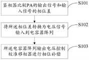
与上述实施例提供的一种功率放大器AM-PM失真校正电路相对应,本申请还提供了一种功率放大器AM-PM失真校正方法的实施例,参见图6,所述方法包括:Corresponding to a power amplifier AM-PM distortion correction circuit provided in the above-mentioned embodiment, the present application also provides an embodiment of a power amplifier AM-PM distortion correction method, see FIG. 6 , the method includes:
S101,鉴相器比较PA的输出信号和输入信号的相位差。S101, the phase detector compares the phase difference between the output signal of the PA and the input signal.
由于鉴相器的第二信号输入端接收到所述PA的原始输入调相信号,而且鉴相器的第一信号输入端与PA的信号输出端又相连接,因此鉴相器可以获取经过PA前后的调相信号,进而比较PA输出相位与输入信号的相位差。Since the second signal input terminal of the phase detector receives the original input phase modulation signal of the PA, and the first signal input terminal of the phase detector is connected to the signal output terminal of the PA, the phase detector can obtain the signal through the PA The phase modulation signal before and after is compared, and then the phase difference between the output phase of the PA and the input signal is compared.
S102,将所述相位差转换为电压信号输入到电容器阵列。S102: Convert the phase difference into a voltage signal and input it to a capacitor array.
具体地,由于电容器阵列与所述鉴相器之间设置有跨导放大器OTA,因此鉴相器将所述相位差转换为电压信号传输给导放大器OTA。输出电压经跨导放大器OTA转换为电流信号输入电容器阵列。Specifically, since a transconductance amplifier OTA is disposed between the capacitor array and the phase detector, the phase detector converts the phase difference into a voltage signal and transmits it to the conduction amplifier OTA. The output voltage is converted into a current signal by the transconductance amplifier OTA and input to the capacitor array.
S103,所述电容器阵列输出电压控制校准移相器进行相位补偿。S103, the output voltage of the capacitor array controls the calibration phase shifter to perform phase compensation.
具体地,不同的选择信号经译码器控制多路复用器选中不同的电容,第一多路复用器和第二多路复用器分别控制与跨导放大器和缓冲放大器之间的连接,电容阵列的输出电压经缓冲放大后控制校准移相器进行相位补偿,反馈环路调整电容上的电压值直到输出与参考信号同相或存在固有的相位差。Specifically, the decoder controls the multiplexer to select different capacitors for different selection signals, and the first multiplexer and the second multiplexer respectively control the connection with the transconductance amplifier and the buffer amplifier. , the output voltage of the capacitor array is buffered and amplified to control the calibration phase shifter to perform phase compensation, and the feedback loop adjusts the voltage value on the capacitor until the output is in phase with the reference signal or has an inherent phase difference.
本申请实施例中,由于刚上电时电容器阵列内电容的电压无法确定,需要进行清零操作,并等待工作达到稳定状态。具体地,对电容器阵列中所有电容进行放电,按照幅度控制码切换电容阵列,当所述电容器阵列达到稳定状态时,电容器阵列初始化完成。In the embodiment of the present application, since the voltage of the capacitor in the capacitor array cannot be determined when the power is just turned on, it is necessary to perform a zero-clearing operation and wait for the operation to reach a stable state. Specifically, all capacitors in the capacitor array are discharged, and the capacitor array is switched according to the amplitude control code. When the capacitor array reaches a stable state, the initialization of the capacitor array is completed.
需要说明的是,在本文中,诸如“第一”和“第二”等之类的关系术语仅仅用来将一个实体或者操作与另一个实体或操作区分开来,而不一定要求或者暗示这些实体或操作之间存在任何这种实际的关系或者顺序。而且,术语“包括”、“包含”或者其任何其他变体意在涵盖非排他性的包含,从而使得包括一系列要素的过程、方法、物品或者设备不仅包括那些要素,而且还包括没有明确列出的其他要素,或者是还包括为这种过程、方法、物品或者设备所固有的要素。在没有更多限制的情况下,由语句“包括一个……”限定的要素,并不排除在包括所述要素的过程、方法、物品或者设备中还存在另外的相同要素。It should be noted that, in this document, relational terms such as "first" and "second" etc. are only used to distinguish one entity or operation from another entity or operation, and do not necessarily require or imply these There is no such actual relationship or sequence between entities or operations. Moreover, the terms "comprising", "comprising" or any other variation thereof are intended to encompass a non-exclusive inclusion such that a process, method, article or device that includes a list of elements includes not only those elements, but also includes not explicitly listed or other elements inherent to such a process, method, article or apparatus. Without further limitation, an element qualified by the phrase "comprising a..." does not preclude the presence of additional identical elements in a process, method, article or apparatus that includes the element.
当然,上述说明也并不仅限于上述举例,本申请未经描述的技术特征可以通过或采用现有技术实现,在此不再赘述;以上实施例及附图仅用于说明本申请的技术方案并非是对本申请的限制,如来替代,本申请仅结合并参照优选的实施方式进行了详细说明,本领域的普通技术人员应当理解,本技术领域的普通技术人员在本申请的实质范围内所做出的变化、改型、添加或替换都不脱离本申请的宗旨,也应属于本申请的权利要求保护范围。Of course, the above description is not limited to the above examples, and the technical features not described in this application can be realized by or using existing technologies, and will not be repeated here; the above embodiments and drawings are only used to illustrate the technical solutions of this application, not It is a limitation of the present application. If it is replaced, the present application is only described in detail with reference to the preferred embodiments. Those of ordinary skill in the art should understand that those of ordinary skill in the art can make Changes, modifications, additions or substitutions do not depart from the purpose of the present application, and should also belong to the protection scope of the claims of the present application.
Claims (10)
Priority Applications (1)
| Application Number | Priority Date | Filing Date | Title |
|---|---|---|---|
| CN201911038882.XACN110798155A (en) | 2019-10-29 | 2019-10-29 | A power amplifier AM-PM distortion correction circuit and method |
Applications Claiming Priority (1)
| Application Number | Priority Date | Filing Date | Title |
|---|---|---|---|
| CN201911038882.XACN110798155A (en) | 2019-10-29 | 2019-10-29 | A power amplifier AM-PM distortion correction circuit and method |
Publications (1)
| Publication Number | Publication Date |
|---|---|
| CN110798155Atrue CN110798155A (en) | 2020-02-14 |
Family
ID=69442070
Family Applications (1)
| Application Number | Title | Priority Date | Filing Date |
|---|---|---|---|
| CN201911038882.XAPendingCN110798155A (en) | 2019-10-29 | 2019-10-29 | A power amplifier AM-PM distortion correction circuit and method |
Country Status (1)
| Country | Link |
|---|---|
| CN (1) | CN110798155A (en) |
Cited By (13)
| Publication number | Priority date | Publication date | Assignee | Title |
|---|---|---|---|---|
| CN111917920A (en)* | 2020-08-12 | 2020-11-10 | 上海剑桥科技股份有限公司 | Intelligent loop holding device |
| CN112543005A (en)* | 2021-02-18 | 2021-03-23 | 广州慧智微电子有限公司 | Amplitude modulation to phase modulation compensation circuit, radio frequency power amplifier and equipment |
| US11942899B2 (en) | 2021-06-18 | 2024-03-26 | Qorvo Us, Inc. | Envelope tracking voltage correction in a transmission circuit |
| US11962338B2 (en) | 2021-09-16 | 2024-04-16 | Qorvo Us, Inc. | Equalization filter calibration in a transceiver circuit |
| US12057813B2 (en) | 2021-06-18 | 2024-08-06 | Qorvo Us, Inc. | Wideband transmission circuit |
| US12199577B2 (en) | 2021-06-18 | 2025-01-14 | Qorvo Us, Inc. | Envelope tracking voltage correction in a transmission circuit |
| US12206365B2 (en) | 2021-06-18 | 2025-01-21 | Qorvo Us, Inc. | Voltage ripple suppression in a transmission circuit |
| US12231088B2 (en) | 2021-06-18 | 2025-02-18 | Qorvo Us, Inc. | Wideband transmission circuit |
| US12273081B2 (en) | 2022-01-27 | 2025-04-08 | Qorvo Us, Inc. | Voltage ripple reduction in a power management circuit |
| US12284003B2 (en) | 2021-09-16 | 2025-04-22 | Qorvo Us, Inc. | Phase and amplitude error correction in a transmission circuit |
| US12323174B2 (en) | 2021-09-16 | 2025-06-03 | Qorvo Us, Inc. | Amplitude-to-phase error correction in a transceiver circuit |
| US12381525B2 (en) | 2022-06-28 | 2025-08-05 | Qorvo Us, Inc. | Amplifier system |
| US12401332B2 (en) | 2021-09-16 | 2025-08-26 | Qorvo Us, Inc. | Phase and amplitude error correction in a transmission circuit |
Citations (9)
| Publication number | Priority date | Publication date | Assignee | Title |
|---|---|---|---|---|
| CN1428923A (en)* | 2001-12-25 | 2003-07-09 | 株式会社日立制作所 | Semiconductor integrated circuit device |
| CN1516493A (en)* | 2003-01-10 | 2004-07-28 | 深圳市中兴通讯股份有限公司上海第二 | A kind of power amplifier linearization method and linear power amplifier device |
| CN101040441A (en)* | 2004-10-12 | 2007-09-19 | 索尼株式会社 | Sample hold circuit, and pipeline ad converter using the circuit |
| CN105207627A (en)* | 2015-09-10 | 2015-12-30 | 鑫高益医疗设备股份有限公司 | Phase calibration structure of magnetic resonance radio frequency power amplifier |
| CN106712730A (en)* | 2016-11-30 | 2017-05-24 | 上海集成电路研发中心有限公司 | Programmable gain amplifier capable of adjusting signals |
| CN107294503A (en)* | 2017-05-27 | 2017-10-24 | 东莞中子科学中心 | An Impedance Automatic Tuning System Capable of Real-time Monitoring and Automatic Compensation |
| CN108551333A (en)* | 2018-03-29 | 2018-09-18 | 广州慧智微电子有限公司 | Rf power amplifier circuit |
| CN109449556A (en)* | 2018-10-23 | 2019-03-08 | 电子科技大学 | The double notch resonators of mixed microstrip line/co-planar waveguide, trapper and electronic equipment |
| CN109921756A (en)* | 2019-01-26 | 2019-06-21 | 桂林电子科技大学 | A kind of fully differential operational transconductance amplifier |
- 2019
- 2019-10-29CNCN201911038882.XApatent/CN110798155A/enactivePending
Patent Citations (9)
| Publication number | Priority date | Publication date | Assignee | Title |
|---|---|---|---|---|
| CN1428923A (en)* | 2001-12-25 | 2003-07-09 | 株式会社日立制作所 | Semiconductor integrated circuit device |
| CN1516493A (en)* | 2003-01-10 | 2004-07-28 | 深圳市中兴通讯股份有限公司上海第二 | A kind of power amplifier linearization method and linear power amplifier device |
| CN101040441A (en)* | 2004-10-12 | 2007-09-19 | 索尼株式会社 | Sample hold circuit, and pipeline ad converter using the circuit |
| CN105207627A (en)* | 2015-09-10 | 2015-12-30 | 鑫高益医疗设备股份有限公司 | Phase calibration structure of magnetic resonance radio frequency power amplifier |
| CN106712730A (en)* | 2016-11-30 | 2017-05-24 | 上海集成电路研发中心有限公司 | Programmable gain amplifier capable of adjusting signals |
| CN107294503A (en)* | 2017-05-27 | 2017-10-24 | 东莞中子科学中心 | An Impedance Automatic Tuning System Capable of Real-time Monitoring and Automatic Compensation |
| CN108551333A (en)* | 2018-03-29 | 2018-09-18 | 广州慧智微电子有限公司 | Rf power amplifier circuit |
| CN109449556A (en)* | 2018-10-23 | 2019-03-08 | 电子科技大学 | The double notch resonators of mixed microstrip line/co-planar waveguide, trapper and electronic equipment |
| CN109921756A (en)* | 2019-01-26 | 2019-06-21 | 桂林电子科技大学 | A kind of fully differential operational transconductance amplifier |
Non-Patent Citations (2)
| Title |
|---|
| VERONICA MARQUES;MARK NADESKI: "提高便携式超声波系统的图像质量", 《中国电子商情》* |
| 谭良 等: "可信认证网关系统的原理与设计", 《电子科技大学学报》* |
Cited By (13)
| Publication number | Priority date | Publication date | Assignee | Title |
|---|---|---|---|---|
| CN111917920A (en)* | 2020-08-12 | 2020-11-10 | 上海剑桥科技股份有限公司 | Intelligent loop holding device |
| CN112543005A (en)* | 2021-02-18 | 2021-03-23 | 广州慧智微电子有限公司 | Amplitude modulation to phase modulation compensation circuit, radio frequency power amplifier and equipment |
| US12231088B2 (en) | 2021-06-18 | 2025-02-18 | Qorvo Us, Inc. | Wideband transmission circuit |
| US11942899B2 (en) | 2021-06-18 | 2024-03-26 | Qorvo Us, Inc. | Envelope tracking voltage correction in a transmission circuit |
| US12057813B2 (en) | 2021-06-18 | 2024-08-06 | Qorvo Us, Inc. | Wideband transmission circuit |
| US12199577B2 (en) | 2021-06-18 | 2025-01-14 | Qorvo Us, Inc. | Envelope tracking voltage correction in a transmission circuit |
| US12206365B2 (en) | 2021-06-18 | 2025-01-21 | Qorvo Us, Inc. | Voltage ripple suppression in a transmission circuit |
| US11962338B2 (en) | 2021-09-16 | 2024-04-16 | Qorvo Us, Inc. | Equalization filter calibration in a transceiver circuit |
| US12284003B2 (en) | 2021-09-16 | 2025-04-22 | Qorvo Us, Inc. | Phase and amplitude error correction in a transmission circuit |
| US12323174B2 (en) | 2021-09-16 | 2025-06-03 | Qorvo Us, Inc. | Amplitude-to-phase error correction in a transceiver circuit |
| US12401332B2 (en) | 2021-09-16 | 2025-08-26 | Qorvo Us, Inc. | Phase and amplitude error correction in a transmission circuit |
| US12273081B2 (en) | 2022-01-27 | 2025-04-08 | Qorvo Us, Inc. | Voltage ripple reduction in a power management circuit |
| US12381525B2 (en) | 2022-06-28 | 2025-08-05 | Qorvo Us, Inc. | Amplifier system |
Similar Documents
| Publication | Publication Date | Title |
|---|---|---|
| CN110798155A (en) | A power amplifier AM-PM distortion correction circuit and method | |
| KR101094050B1 (en) | Dynamic Bias Supply with Multiple Switches | |
| US9438186B2 (en) | Power amplifier with envelope injection | |
| CN101911477A (en) | Predistorter | |
| US8736365B2 (en) | Broadband linearization module and method | |
| WO2001082473A1 (en) | Distortion compensation apparatus | |
| CN110729972B (en) | Calibration device and calibration method | |
| US20140112414A1 (en) | Power amplifier and the related power amplifying method | |
| US10516370B2 (en) | Predistorter for compensating linearity of an amplifier | |
| JPH0752812B2 (en) | Predistortion circuit | |
| US4857865A (en) | Self equalizing multi-stage radio frequency power amplifier | |
| US20120242405A1 (en) | Frequency-Desensitizer for Broadband Predistortion Linearizers | |
| US7696822B2 (en) | Amplifying circuit and associated linearity improving method | |
| JPH11355055A (en) | Distortion compensation circuit and low distortion semiconductor amplifier | |
| US20170324386A1 (en) | Rf class ab cascode amplifier with linearization and steering diodes | |
| US20110026638A1 (en) | Positive coefficient weighted quadrature modulation method and apparatus | |
| JP2014138323A (en) | Amplification device, distortion compensation device and distortion compensation method | |
| JP2005150932A (en) | Pre-distortion device | |
| Nguyen et al. | Design of a 10.56-Gb/s 64-QAM Polar Transmitter at 60 GHz in 28-nm CMOS | |
| US10187016B2 (en) | Amplifier with improved linearity | |
| US10965252B2 (en) | Broadband driver with extended linear output voltage | |
| KR20090126035A (en) | Switch-Mode Power Amplifiers for Polar Transmitters | |
| US20230412136A1 (en) | Gain equalizer and method for controlling tunable gain of gain equalizer | |
| EP2846460A1 (en) | Arrangement and method for radio frequency power amplification | |
| US8102208B2 (en) | Signal amplifier |
Legal Events
| Date | Code | Title | Description |
|---|---|---|---|
| PB01 | Publication | ||
| PB01 | Publication | ||
| SE01 | Entry into force of request for substantive examination | ||
| SE01 | Entry into force of request for substantive examination | ||
| RJ01 | Rejection of invention patent application after publication | Application publication date:20200214 | |
| RJ01 | Rejection of invention patent application after publication |