CN110797351B - Array substrate, detection method thereof, display panel and display device - Google Patents
Array substrate, detection method thereof, display panel and display deviceDownload PDFInfo
- Publication number
- CN110797351B CN110797351BCN201911087102.0ACN201911087102ACN110797351BCN 110797351 BCN110797351 BCN 110797351BCN 201911087102 ACN201911087102 ACN 201911087102ACN 110797351 BCN110797351 BCN 110797351B
- Authority
- CN
- China
- Prior art keywords
- pixel unit
- extension
- layer
- anode
- array substrate
- Prior art date
- Legal status (The legal status is an assumption and is not a legal conclusion. Google has not performed a legal analysis and makes no representation as to the accuracy of the status listed.)
- Active
Links
Images


Classifications
- H—ELECTRICITY
- H10—SEMICONDUCTOR DEVICES; ELECTRIC SOLID-STATE DEVICES NOT OTHERWISE PROVIDED FOR
- H10D—INORGANIC ELECTRIC SEMICONDUCTOR DEVICES
- H10D86/00—Integrated devices formed in or on insulating or conducting substrates, e.g. formed in silicon-on-insulator [SOI] substrates or on stainless steel or glass substrates
- H10D86/40—Integrated devices formed in or on insulating or conducting substrates, e.g. formed in silicon-on-insulator [SOI] substrates or on stainless steel or glass substrates characterised by multiple TFTs
- H—ELECTRICITY
- H01—ELECTRIC ELEMENTS
- H01L—SEMICONDUCTOR DEVICES NOT COVERED BY CLASS H10
- H01L22/00—Testing or measuring during manufacture or treatment; Reliability measurements, i.e. testing of parts without further processing to modify the parts as such; Structural arrangements therefor
- H01L22/10—Measuring as part of the manufacturing process
- H01L22/12—Measuring as part of the manufacturing process for structural parameters, e.g. thickness, line width, refractive index, temperature, warp, bond strength, defects, optical inspection, electrical measurement of structural dimensions, metallurgic measurement of diffusions
- H—ELECTRICITY
- H10—SEMICONDUCTOR DEVICES; ELECTRIC SOLID-STATE DEVICES NOT OTHERWISE PROVIDED FOR
- H10D—INORGANIC ELECTRIC SEMICONDUCTOR DEVICES
- H10D86/00—Integrated devices formed in or on insulating or conducting substrates, e.g. formed in silicon-on-insulator [SOI] substrates or on stainless steel or glass substrates
- H10D86/40—Integrated devices formed in or on insulating or conducting substrates, e.g. formed in silicon-on-insulator [SOI] substrates or on stainless steel or glass substrates characterised by multiple TFTs
- H10D86/60—Integrated devices formed in or on insulating or conducting substrates, e.g. formed in silicon-on-insulator [SOI] substrates or on stainless steel or glass substrates characterised by multiple TFTs wherein the TFTs are in active matrices
- H—ELECTRICITY
- H10—SEMICONDUCTOR DEVICES; ELECTRIC SOLID-STATE DEVICES NOT OTHERWISE PROVIDED FOR
- H10K—ORGANIC ELECTRIC SOLID-STATE DEVICES
- H10K50/00—Organic light-emitting devices
- H10K50/80—Constructional details
- H10K50/805—Electrodes
- H10K50/81—Anodes
- H—ELECTRICITY
- H10—SEMICONDUCTOR DEVICES; ELECTRIC SOLID-STATE DEVICES NOT OTHERWISE PROVIDED FOR
- H10K—ORGANIC ELECTRIC SOLID-STATE DEVICES
- H10K50/00—Organic light-emitting devices
- H10K50/80—Constructional details
- H10K50/86—Arrangements for improving contrast, e.g. preventing reflection of ambient light
- H—ELECTRICITY
- H10—SEMICONDUCTOR DEVICES; ELECTRIC SOLID-STATE DEVICES NOT OTHERWISE PROVIDED FOR
- H10K—ORGANIC ELECTRIC SOLID-STATE DEVICES
- H10K59/00—Integrated devices, or assemblies of multiple devices, comprising at least one organic light-emitting element covered by group H10K50/00
- H10K59/10—OLED displays
- H10K59/12—Active-matrix OLED [AMOLED] displays
Landscapes
- Engineering & Computer Science (AREA)
- Manufacturing & Machinery (AREA)
- Microelectronics & Electronic Packaging (AREA)
- Physics & Mathematics (AREA)
- Optics & Photonics (AREA)
- Computer Hardware Design (AREA)
- Power Engineering (AREA)
- Electroluminescent Light Sources (AREA)
- Devices For Indicating Variable Information By Combining Individual Elements (AREA)
Abstract
Translated fromChinese
Description
Translated fromChinese技术领域technical field
本发明涉及显示技术领域,特别涉及一种阵列基板、其检测方法、显示面板及显示装置。The present invention relates to the field of display technology, and in particular, to an array substrate, a detection method thereof, a display panel and a display device.
背景技术Background technique
有机发光二极管(Organic Light Emitting Diode,OLED)是当今平板显示器研究领域的热点之一,与液晶显示器(Liquid Crystal Display,LCD)相比,OLED显示器具有低能耗、生产成本低、自发光、宽视角及响应速度快等优点。目前,在手机、平板电脑、数码相机等显示领域,OLED显示器已经开始取代传统的LCD显示器。Organic Light Emitting Diode (OLED) is one of the hotspots in the research field of flat panel display today. Compared with Liquid Crystal Display (LCD), OLED display has the advantages of low energy consumption, low production cost, self-luminescence and wide viewing angle. and fast response. At present, OLED displays have begun to replace traditional LCD displays in display fields such as mobile phones, tablet computers, and digital cameras.
发明内容SUMMARY OF THE INVENTION
本发明实施例提供一种阵列基板、其检测方法、显示面板及显示装置,用以解决现有技术中像素由于Particle异物导致的short不良,进而导致点灯画面显示亮点或暗点不良,严重影响画面品质的问题。Embodiments of the present invention provide an array substrate, a detection method thereof, a display panel and a display device, which are used to solve the problem of short defects in pixels caused by foreign particles of Particles in the prior art, which in turn leads to poor bright or dark spots on a lighting screen, which seriously affects the screen. quality issue.
因此,本发明实施例提供了一种阵列基板,包括呈阵列分布的多个像素单元,每一所述像素单元包括位于衬底基板上层叠设置的遮光部、薄膜晶体管以及与所述遮光部电连接的阳极;其中,Therefore, an embodiment of the present invention provides an array substrate, which includes a plurality of pixel units distributed in an array, and each pixel unit includes a light shielding portion, a thin film transistor, and an electrical connection with the light shielding portion stacked on the base substrate. connected anodes; where,
在任意一个所述像素单元内,所述遮光部具有向其中一个相邻且发光颜色相同的像素单元方向延伸的第一延伸部,所述阳极具有向另一个相邻且发光颜色相同的像素单元方向延伸的第二延伸部;In any one of the pixel units, the light-shielding portion has a first extension portion extending toward one of the adjacent pixel units with the same emission color, and the anode has a first extension toward the other adjacent pixel units with the same emission color a second extension extending in the direction;
在相邻且发光颜色相同的两个所述像素单元内,其中一个所述像素单元内的第一延伸部和另一个所述像素单元内的第二延伸部在所述衬底基板上的正投影具有交叠区域,且所述第一延伸部和所述第二延伸部相互绝缘。In two adjacent pixel units with the same emission color, the first extension part in one of the pixel units and the second extension part in the other pixel unit are on the positive side of the base substrate The projections have overlapping regions, and the first extension portion and the second extension portion are insulated from each other.
可选地,在具体实施时,在本发明实施例提供的上述阵列基板中,还包括:位于所述薄膜晶体管和所述阳极之间的钝化层,以及位于所述钝化层和所述阳极之间的平坦化层;所述第二延伸部通过贯穿所述平坦化层的第一过孔与所述钝化层接触。Optionally, during specific implementation, the above-mentioned array substrate provided in the embodiment of the present invention further includes: a passivation layer located between the thin film transistor and the anode, and a passivation layer located between the passivation layer and the anode. a planarization layer between anodes; the second extension is in contact with the passivation layer through a first via hole penetrating the planarization layer.
可选地,在具体实施时,在本发明实施例提供的上述阵列基板中,还包括:位于所述钝化层与所述平坦化层之间的色阻层,所述色阻层与所述交叠区域不重叠。Optionally, during specific implementation, the above-mentioned array substrate provided in the embodiment of the present invention further includes: a color resist layer located between the passivation layer and the planarization layer, and the color resist layer is connected to the color resist layer. The overlapping regions do not overlap.
可选地,在具体实施时,在本发明实施例提供的上述阵列基板中,还包括:位于所述遮光部与所述薄膜晶体管之间的缓冲层,位于所述缓冲层与所述钝化层之间的层间绝缘层,以及位于所述钝化层与所述第一延伸部之间的搭接部;Optionally, during specific implementation, the array substrate provided in the embodiment of the present invention further includes: a buffer layer located between the light shielding portion and the thin film transistor, located between the buffer layer and the passivation an interlayer insulating layer between layers, and an overlap portion between the passivation layer and the first extension;
所述搭接部通过贯穿所述缓冲层和所述层间绝缘层的第二过孔与所述第一延伸部电连接,所述搭接部和所述第二延伸部在所述衬底基板上的正投影具有交叠区域。The overlap portion is electrically connected to the first extension portion through a second via hole penetrating the buffer layer and the interlayer insulating layer, and the overlap portion and the second extension portion are located on the substrate. The orthographic projections on the substrate have overlapping regions.
可选地,在具体实施时,在本发明实施例提供的上述阵列基板中,所述搭接部与所述薄膜晶体管的漏极同层设置。Optionally, in the specific implementation, in the above-mentioned array substrate provided in the embodiment of the present invention, the overlapping portion and the drain electrode of the thin film transistor are provided in the same layer.
可选地,在具体实施时,在本发明实施例提供的上述阵列基板中,在每一所述像素单元内,所述阳极通过贯穿所述钝化层的第三过孔与所述薄膜晶体管的漏极电连接,所述薄膜晶体管的漏极通过贯穿所述层间绝缘层和所述缓冲层的第四过孔与所述遮光部电连接。Optionally, during specific implementation, in the above-mentioned array substrate provided by the embodiment of the present invention, in each pixel unit, the anode communicates with the thin film transistor through a third via hole penetrating the passivation layer The drain of the thin film transistor is electrically connected to the light-shielding portion through a fourth via hole penetrating through the interlayer insulating layer and the buffer layer.
相应地,本发明实施例还提供了一种显示面板,包括本发明实施例提供的上述任一阵列基板。Correspondingly, an embodiment of the present invention further provides a display panel, including any of the above-mentioned array substrates provided by the embodiment of the present invention.
相应地,本发明实施例还提供了一种显示装置,包括本发明实施例提供的上述显示面板。Correspondingly, an embodiment of the present invention further provides a display device, including the above-mentioned display panel provided by the embodiment of the present invention.
相应地,本发明实施例还提供了一种阵列基板的检测方法,包括:Correspondingly, an embodiment of the present invention also provides a method for detecting an array substrate, including:
在点灯测试阶段,若存在异常像素单元,则通过激光熔融的方式使与所述异常像素单元相邻且发光颜色相同的正常像素单元内的第一延伸部与所述异常像素单元内的第二延伸部电连接,以使所述正常像素单元内的阳极与所述异常像素单元内的阳极导通。In the lighting test stage, if there is an abnormal pixel unit, the first extension in the normal pixel unit adjacent to the abnormal pixel unit and with the same emission color and the second extension in the abnormal pixel unit are made by laser melting. The extension part is electrically connected to make the anode in the normal pixel unit conduct with the anode in the abnormal pixel unit.
可选地,在具体实施时,在本发明实施例提供的上述检测方法中,在激光熔融所述交叠区域对应的钝化层之前,还包括:Optionally, during specific implementation, in the above-mentioned detection method provided by the embodiment of the present invention, before the laser melting of the passivation layer corresponding to the overlapping region, the method further includes:
采用激光熔融所述薄膜晶体管的有源层,以断开所述薄膜晶体管。A laser is used to melt the active layer of the thin film transistor to disconnect the thin film transistor.
本发明实施例的有益效果包括:The beneficial effects of the embodiments of the present invention include:
本发明实施例提供的阵列基板、其检测方法、显示面板及显示装置,本发明通过在任意一个像素单元内,将遮光部设置具有向其中一个相邻且发光颜色相同的像素单元方向延伸的第一延伸部,将阳极设置具有向另一个相邻且发光颜色相同的像素单元方向延伸的第二延伸部;在相邻且发光颜色相同的两个像素单元内,其中一个像素单元内的第一延伸部和另一个像素单元内的第二延伸部在衬底基板上的正投影具有交叠区域,且第一延伸部和第二延伸部相互绝缘。这样在任意一像素单元内的缓冲层、有源层、ITO等工艺过程中产生Particle导致short不良时,可通过激光熔融的方式使与该发生short不良的异常像素单元相邻且发光颜色相同的正常像素单元内的第一延伸部与该异常像素单元内的第二延伸部电连接,即使异常像素单元内的阳极与正常像素单元内的阳极电连接,从而通过正常像素单元驱动异常像素单元正常发光,可以将亮点和暗点像素单元维修成正常的像素单元,提升画面的显示效果,并且本发明只需要改变遮光部和阳极的构图工艺,不需要增加其它工艺和膜层,实现维修异常像素单元的工艺较简单。In the array substrate, the detection method, the display panel, and the display device provided by the embodiments of the present invention, the present invention provides a light shielding portion in any pixel unit with a second pixel unit extending in the direction of one of the adjacent pixel units with the same light emission color. an extension part, the anode is provided with a second extension part extending in the direction of another adjacent pixel unit with the same emission color; in the two adjacent pixel units with the same emission color, the first extension in one pixel unit The orthographic projection of the extension part and the second extension part in another pixel unit on the base substrate has an overlapping area, and the first extension part and the second extension part are insulated from each other. In this way, when Particles are generated in the buffer layer, active layer, ITO and other processes in any pixel unit and cause short defects, laser melting can be used to make the abnormal pixel unit with short defects adjacent to the abnormal pixel unit with the same emission color. The first extension in the normal pixel unit is electrically connected with the second extension in the abnormal pixel unit, even if the anode in the abnormal pixel unit is electrically connected with the anode in the normal pixel unit, so that the abnormal pixel unit is driven by the normal pixel unit to be normal. Lighting, the bright and dark pixel units can be repaired into normal pixel units, and the display effect of the picture is improved, and the present invention only needs to change the patterning process of the shading part and the anode, and does not need to add other processes and film layers, so as to realize the maintenance of abnormal pixels. The process of the unit is relatively simple.
附图说明Description of drawings
图1为相关技术中阵列基板的俯视结构示意图;FIG. 1 is a schematic top-view structure diagram of an array substrate in the related art;
图2为图1所示的阵列基板发生像素发光异常的示意图;FIG. 2 is a schematic diagram of abnormal pixel light emission of the array substrate shown in FIG. 1;
图3为本发明实施例提供的阵列基板的剖面结构示意图之一;FIG. 3 is a schematic cross-sectional structure diagram of an array substrate provided by an embodiment of the present invention;
图4为图3所示的阵列基板的俯视结构示意图;FIG. 4 is a schematic top view of the structure of the array substrate shown in FIG. 3;
图5为本发明实施例提供的阵列基板的剖面结构示意图之二;FIG. 5 is a second schematic diagram of a cross-sectional structure of an array substrate according to an embodiment of the present invention;
图6A-图6D为本发明实施例提供的阵列基板的制作方法在执行每一步骤之后的剖面结构示意图;6A-6D are schematic cross-sectional structural diagrams of a method for fabricating an array substrate according to an embodiment of the present invention after each step is performed;
图7为本发明实施例提供的阵列基板中每一像素单元的电容结构示意图。FIG. 7 is a schematic diagram of a capacitor structure of each pixel unit in an array substrate according to an embodiment of the present invention.
具体实施方式Detailed ways
为了使本发明的目的,技术方案和优点更加清楚,下面结合附图,对本发明实施例提供的阵列基板、其制作方法、显示面板及显示装置的具体实施方式进行详细地说明。In order to make the purpose, technical solutions and advantages of the present invention clearer, the specific implementations of the array substrate, its manufacturing method, the display panel and the display device provided by the embodiments of the present invention are described in detail below with reference to the accompanying drawings.
附图中各层薄膜厚度和形状不反映阵列基板的真实比例,目的只是示意说明本发明内容。The thickness and shape of each layer in the drawings do not reflect the real scale of the array substrate, and are only intended to illustrate the content of the present invention.
相关技术中,如图1所示,OLED的阵列基板包括位于衬底基板上的遮光部01、缓冲层02、栅极层03、有源层04、源漏电极层05和阳极层06,目前在Array工艺制备上述膜层过程中,Buffer(缓冲层01)、IGZO(有源层04)、ITO(阳极层06)等工艺中由于Particle类异物容易导致IGZO-Gate/SD或ITO-EL电极之间的short类不良,如图1中的黑点位置处;在进行点灯测试时,如图2所示,导致点灯画面显示亮点或暗点不良,严重影响画面品质。在上述Array、面板修复过程中,目前仅能将可见的线不良和亮点不良进行暗点化处理,无法维修成OK状态;在存在较多线不良和亮点不良时,即使能够维修,也会影响画面的显示效果(面板报废标准:暗点>10颗,亮点>0颗,线>0条),导致面板报废处理。In the related art, as shown in FIG. 1, an OLED array substrate includes a
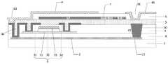
有鉴于此,本发明实施例提供的阵列基板,如图3和图4所示,图3为本发明实施例提供的阵列基板的剖面结构示意图,图4为图3所示的阵列基板的俯视结构示意图,包括呈阵列分布的多个像素单元,每一像素单元包括位于衬底基板1上层叠设置的遮光部2、薄膜晶体管3以及与遮光部2电连接的阳极4;其中,In view of this, the array substrate provided by the embodiment of the present invention is shown in FIG. 3 and FIG. 4 . FIG. 3 is a schematic cross-sectional structure diagram of the array substrate provided by the embodiment of the present invention, and FIG. 4 is a top view of the array substrate shown in FIG. 3 . The schematic structural diagram includes a plurality of pixel units distributed in an array, and each pixel unit includes a light-
在任意一个像素单元内,遮光部2具有向其中一个相邻且发光颜色相同的像素单元方向延伸的第一延伸部21,阳极4具有向另一个相邻且发光颜色相同的像素单元方向延伸的第二延伸部41;In any pixel unit, the light-
在相邻且发光颜色相同的两个像素单元内,其中一个像素单元内的第一延伸部21和另一个像素单元内的第二延伸部41在衬底基板1上的正投影具有交叠区域,且第一延伸部21和第二延伸部41相互绝缘;本发明实施例图3仅示意出相邻两个发光颜色相同的像素单元的部分结构,其中左侧的像素单元仅示意出其遮光部2具有向右侧像素单元方向延伸的第一延伸部21,而左侧像素单元的阳极4向左侧延伸的第二延伸部41没有示意出,右侧像素单元仅示意出其阳极4向左侧像素单元延伸的第二延伸部41,而右侧像素单元的遮光部2向右侧像素单元方向延伸的第一延伸部21没有示意出,图3仅是为了示意解释本发明。In two adjacent pixel units with the same emission color, the orthographic projection of the
本发明实施例提供的上述阵列基板,通过在任意一个像素单元内,将遮光部2设置具有向其中一个相邻且发光颜色相同的像素单元方向延伸的第一延伸部21,将阳极4设置具有向另一个相邻且发光颜色相同的像素单元方向延伸的第二延伸部41;在相邻且发光颜色相同的两个像素单元内,其中一个像素单元内的第一延伸部21和另一个像素单元内的第二延伸部41在衬底基板1上的正投影具有交叠区域,且第一延伸部21和第二延伸部41相互绝缘。这样在任意一像素单元内的缓冲层、有源层、ITO等工艺过程中产生Particle导致short不良时,可通过激光熔融的方式使与该发生short不良的异常像素单元(如图3中右侧像素单元)相邻且发光颜色相同的正常像素单元(如图3中左侧像素单元)内的第一延伸部21与该异常像素单元内的第二延伸部41电连接,即使异常像素单元内的阳极4与正常像素单元内的阳极4电连接,从而通过正常像素单元驱动异常像素单元正常发光,可以将亮点和暗点像素单元维修成正常的像素单元,提升画面的显示效果,并且本发明只需要改变遮光部和阳极的构图工艺,不需要增加其它工艺和膜层,实现维修异常像素单元的工艺较简单。In the above-mentioned array substrate provided by the embodiment of the present invention, in any pixel unit, the light-
需要说明的是,第一延伸部和第二延伸部相互绝缘是指在像素单元正常发光时,第一延伸部和第二延伸部之间具有绝缘层而不电连接,只有在像素单元发生异常(点灯画面显示亮点或暗点)的时候,才利用激光熔融第一延伸部和第二延伸部之间的绝缘层,因此在像素单元正常发光时,第一延伸部和第二延伸部不影响正常显示功能。It should be noted that the mutual insulation between the first extension part and the second extension part means that when the pixel unit emits light normally, there is an insulating layer between the first extension part and the second extension part and is not electrically connected, and only when the pixel unit is abnormal When the lighting screen shows bright spots or dark spots, the insulating layer between the first extension part and the second extension part is melted by laser. Therefore, when the pixel unit emits light normally, the first extension part and the second extension part do not affect the Normal display function.
可选地,在具体实施时,在本发明实施例提供的上述阵列基板中,如图3所示,还包括:位于薄膜晶体管3和阳极4之间的钝化层5,以及位于钝化层5和阳极4之间的平坦化层6;由于阳极4膜层的膜厚较薄,为了保证在激光熔融第二延伸部41和第一延伸部21之间绝缘层时能够使第二延伸部41和第一延伸部21电连接成功,而不出现断线的风险,就需要在保证不影响正常显示时尽可能的降低第二延伸部41和第一延伸部21之间的绝缘层的厚度,因此将第二延伸部41通过贯穿平坦化层6的第一过孔01与钝化层5接触,这样可以使第二延伸部41和第一延伸部21之间减少一层平坦化层6,从而可以提高通过激光熔融使第二延伸部41和第一延伸部21电连接成功的概率。Optionally, during specific implementation, the above-mentioned array substrate provided in the embodiment of the present invention, as shown in FIG. 3 , further includes: a
在具体实施时,平坦化层的材料可以为树脂材料,树脂材料的平坦化层可以提高阳极与基板之间的附着力。In a specific implementation, the material of the planarization layer may be a resin material, and the planarization layer of the resin material may improve the adhesion between the anode and the substrate.
可选地,在具体实施时,在本发明实施例提供的上述阵列基板中,如图3所示,还包括:位于钝化层5与平坦化层6之间的色阻层7,色阻层7与交叠区域不重叠。具体地,本发明通过将色阻层7设置在钝化层5与平坦化层6之间,即采用的是底发射型发光,色阻层可以包括不同颜色的色阻,如红色(R)色阻、绿色(G)色阻和蓝色(B)色阻,还可以包括其它颜色如黄色色阻等,色阻层7与交叠区域不重叠,这样在发生异常像素单元时,通过激光熔融的方式使交叠区域的绝缘层熔融而使第二延伸部41和第一延伸部21电连接时,由于色阻层7与交叠区域不重叠,因此激光熔融不会破坏色阻层7的色阻。Optionally, during specific implementation, in the above-mentioned array substrate provided in the embodiment of the present invention, as shown in FIG. 3 , further includes: a color resist layer 7 located between the
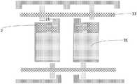
可选地,在具体实施时,在本发明实施例提供的上述阵列基板中,如图3所示,还包括:位于遮光部2与薄膜晶体管3之间的缓冲层8,位于缓冲层8与钝化层5之间的层间绝缘层9,由于图3中的第二延伸部41与第一延伸部21之间具有钝化层5、层间绝缘层9和缓冲层8,使得第二延伸部41与第一延伸部21之间的距离较远,由于阳极4厚度较薄,因此在发生异常像素需要激光熔融使第二延伸部41与第一延伸部21电连接时,容易发生第二延伸部41与第一延伸部21搭接不成功的风险;因此,为了确保第二延伸部41与第一延伸部21能够搭接成功,如图5所示,本发明实施例提供的阵列基板还包括位于钝化层5与第一延伸部21之间的搭接部10;Optionally, during specific implementation, the above-mentioned array substrate provided in the embodiment of the present invention, as shown in FIG. 3 , further includes: a
搭接部10通过贯穿缓冲层8和层间绝缘层9的第二过孔02与第一延伸部21电连接,搭接部10和第二延伸部41在衬底基板1上的正投影具有交叠区域,这样通过预先设置与第一延伸部21电连接的搭接部10,使得搭接部10和第二延伸部41之间仅具有钝化层5,进一步降低第一延伸部21和第二延伸部41之间搭接的距离,因此在需要激光熔融搭接第一延伸部21和第二延伸部41时,仅需熔融钝化层5,可以保证第二延伸部41和搭接部10电连接成功,从而能够使第一延伸部21和第二延伸部41电连接成功,进一步提高通过激光熔融使第二延伸部41和第一延伸部21电连接成功的概率。The
在具体实施时,在本发明实施例提供的上述阵列基板中,如图3和图5所示,薄膜晶体管3包括位于缓冲层8上依次层叠设置的有源层31、栅绝缘层32、栅极33、源漏极(源极34、漏极35)。In specific implementation, in the above-mentioned array substrate provided by the embodiment of the present invention, as shown in FIG. 3 and FIG. 5 , the
可选地,在具体实施时,在本发明实施例提供的上述阵列基板中,如图5所示,搭接部10与薄膜晶体管3的漏极35同层设置。这样,只需要在形成薄膜晶体管3的漏极35时改变原有的构图图形,即可通过一次构图工艺形成搭接部10与漏极35的图形,不用增加单独制备搭接部10的工艺,可以简化制备工艺流程,节省生产成本,提高生产效率。Optionally, in the specific implementation, in the above-mentioned array substrate provided in the embodiment of the present invention, as shown in FIG. In this way, it is only necessary to change the original patterning pattern when forming the
可选地,在具体实施时,在本发明实施例提供的上述阵列基板中,如图3和图5所示,在每一像素单元内,阳极4通过贯穿钝化层5的第三过孔03与薄膜晶体管3的漏极35电连接,薄膜晶体管3的漏极35通过贯穿层间绝缘层9和缓冲层8的第四过孔04与遮光部2电连接。即本发明实施例中像素单元的阳极4是通过漏极35与遮光部2电连接,因此可通过正常像素单元向异常像素单元直接提供阳极电压和电流。Optionally, during specific implementation, in the above-mentioned array substrate provided in the embodiment of the present invention, as shown in FIG. 3 and FIG. 5 , in each pixel unit, the
基于同一发明构思,本发明实施例还提供了一种阵列基板的检测方法,包括:Based on the same inventive concept, an embodiment of the present invention also provides a detection method for an array substrate, including:
在点灯测试阶段,若存在异常像素单元,则通过激光熔融的方式使与异常像素单元相邻且发光颜色相同的正常像素单元内的第一延伸部与异常像素单元内的第二延伸部电连接,以使正常像素单元内的阳极与异常像素单元内的阳极导通。In the lighting test stage, if there is an abnormal pixel unit, the first extension in the normal pixel unit adjacent to the abnormal pixel unit and with the same emission color is electrically connected to the second extension in the abnormal pixel unit by laser melting. , so that the anode in the normal pixel unit is conductive with the anode in the abnormal pixel unit.
本发明实施例提供的阵列基板的检测方法,在任意一像素单元内的缓冲层、有源层、ITO等工艺过程中产生Particle导致short不良时,可通过激光熔融的方式使与该发生short不良的异常像素单元相邻且发光颜色相同的正常像素单元内的第一延伸部与该异常像素单元内的第二延伸部电连接,即使异常像素单元内的阳极与正常像素单元内的阳极电连接,从而通过正常像素单元驱动异常像素单元正常发光,改善画面显示品质。In the detection method of the array substrate provided by the embodiment of the present invention, when short defects are caused by particles generated in the buffer layer, active layer, ITO and other processes in any pixel unit, the short defects can be caused by laser melting. The first extension in the abnormal pixel unit adjacent to the normal pixel unit with the same emission color is electrically connected with the second extension in the abnormal pixel unit, even if the anode in the abnormal pixel unit is electrically connected with the anode in the normal pixel unit. , so that the abnormal pixel unit is driven by the normal pixel unit to emit light normally, and the picture display quality is improved.
具体地,如图5所示,在点灯测试阶段,若存在异常像素单元(如图5中右侧像素单元),则通过激光熔融的方式熔融第一延伸部21和第二延伸部41之间的钝化层5,使异常像素单元的第二延伸部41与搭接部10电连接,从而使与异常像素单元相邻且发光颜色相同的正常像素单元(图5中左侧像素单元)内的第一延伸部21与异常像素单元内的第二延伸部41(图5中右侧像素单元)电连接,即使正常像素单元内的阳极4与异常像素单元内的阳极4导通。Specifically, as shown in FIG. 5 , in the lighting test stage, if there is an abnormal pixel unit (the right pixel unit in FIG. 5 ), the space between the
可选地,在具体实施时,在本发明实施例提供的上述阵列基板中,在激光熔融交叠区域对应的钝化层之前,还包括:Optionally, during specific implementation, in the above-mentioned array substrate provided in the embodiment of the present invention, before the laser melts the passivation layer corresponding to the overlapping region, the method further includes:
采用激光熔融薄膜晶体管的有源层,以断开薄膜晶体管。A laser is used to melt the active layer of the thin film transistor to disconnect the thin film transistor.
具体地,如图5所示,在点灯测试阶段,若存在异常像素单元(如图5中左侧像素单元),在激光熔融交叠区域对应的钝化层5之前,首先采用激光熔融的方式熔融薄膜晶体管3的有源层31,以断开薄膜晶体管3。Specifically, as shown in FIG. 5 , in the lighting test stage, if there is an abnormal pixel unit (the left pixel unit in FIG. 5 ), before laser melting the
下面通过具体实施例对图5所示的阵列基板的制作方法进行详细阐述。The manufacturing method of the array substrate shown in FIG. 5 will be described in detail below through specific embodiments.
(1)在衬底基板上沉积遮光部2,并且每一像素单元内的遮光部2具有向一个相邻且发光颜色相同的像素单元延伸的第一延伸部21,如图6A所示;(1) depositing the light-shielding
(2)在形成有遮光部2的衬底基板上沉积缓冲层,后续沉积金属氧化物薄膜如IGZO材料,通过构图工艺形成有源层31图形,再沉积栅绝缘层(材料可以为SiO2),再沉积一层栅极金属层,此金属材料可为Cu或Al,通过涂胶-曝光-显影-刻蚀-光刻胶剥离,形成栅极33,其中在栅极33刻蚀完成后,进行栅绝缘层刻蚀,然后将栅极33未覆盖的栅绝缘层剥离以及对有源层31进行导体化,如图6B所示,图6B仅示意出有源层31和栅极33的图形;(2) depositing a buffer layer on the base substrate formed with the
(3)在形成有栅极33的衬底基板上沉积一层层间绝缘层(材料可以为SiO2),在与阳极4对应的区域通过刻蚀工艺在层间绝缘层和缓冲层内形成第四过孔04,在与第一延伸部21对应的区域通过刻蚀工艺在层间绝缘层和缓冲层内形成第二过孔02,如图6C所示;(3) Deposit an interlayer insulating layer (the material can be SiO2) on the base substrate on which the
(4)在层间绝缘层上方沉积一层金属层,此金属材料可为Cu或Al,通过构图工艺在第一延伸部21上方保留该金属层以形成搭接部10,再通过刻蚀-剥离等工艺形成源漏极(源极34、漏极35),漏极通过第四过孔04与遮光部2电连接,然后在源漏极(源极34、漏极35)上方沉积一层钝化层(材料可以为SiO2),并在钝化层中与漏极35对应的区域形成第三过孔,如图6D所示;(4) A metal layer is deposited on the interlayer insulating layer, and the metal material can be Cu or Al, and the metal layer is retained above the
(5)在钝化层上方沉积色阻层,在色阻层上方沉积平坦化层,并在平坦化层中与第一延伸部21对应的区域形成第一过孔,然后在平坦化层上方沉积ITO电极层,通过涂胶-曝光-刻蚀-剥离一系列工序形成阳极4,并且阳极具有向另一个相邻且发光颜色相同的像素单元延伸的第二延伸部41,如图4所示;阳极4和遮光部2通过第三过孔与漏极35电连接,如图7所示的电容结构,因此可通过正常像素向异常像素直接提供阳极电压和电流。(5) depositing a color resist layer over the passivation layer, depositing a planarization layer over the color resist layer, and forming a first via hole in the planarization layer in a region corresponding to the
通过上述实施例一的步骤(1)至步骤(5)后可以得到本发明实施例提供的图5所示的探测面板。After steps (1) to (5) of the first embodiment above, the detection panel shown in FIG. 5 can be obtained according to the embodiment of the present invention.
基于同一发明构思,本发明实施例还提供了一种显示面板,包括本发明实施例提供的上述任一种阵列基板。该显示面板解决问题的原理与前述阵列基板相似,因此该显示面板的实施可以参见前述阵列基板的实施,重复之处在此不再赘述。Based on the same inventive concept, an embodiment of the present invention further provides a display panel, including any of the array substrates provided in the embodiment of the present invention. The problem-solving principle of the display panel is similar to that of the aforementioned array substrate. Therefore, the implementation of the display panel can refer to the aforementioned implementation of the array substrate, and the repetition will not be repeated here.
基于同一发明构思,本发明实施例还提供了一种显示装置,包括本发明实施例提供的上述显示面板。该显示装置解决问题的原理与前述显示面板相似,因此该显示装置的实施可以参见前述显示面板的实施,重复之处在此不再赘述。Based on the same inventive concept, an embodiment of the present invention further provides a display device, including the above-mentioned display panel provided by an embodiment of the present invention. The problem-solving principle of the display device is similar to that of the aforementioned display panel. Therefore, the implementation of the display device can refer to the aforementioned implementation of the display panel, and repeated details will not be repeated here.
本发明实施例提供的阵列基板、其检测方法、显示面板及显示装置,本发明通过在任意一个像素单元内,将遮光部设置具有向其中一个相邻且发光颜色相同的像素单元方向延伸的第一延伸部,将阳极设置具有向另一个相邻且发光颜色相同的像素单元方向延伸的第二延伸部;在相邻且发光颜色相同的两个像素单元内,其中一个像素单元内的第一延伸部和另一个像素单元内的第二延伸部在衬底基板上的正投影具有交叠区域,且第一延伸部和第二延伸部相互绝缘。这样在任意一像素单元内的缓冲层、有源层、ITO等工艺过程中产生Particle导致short不良时,可通过激光熔融的方式使与该发生short不良的异常像素单元相邻且发光颜色相同的正常像素单元内的第一延伸部与该异常像素单元内的第二延伸部电连接,即使异常像素单元内的阳极与正常像素单元内的阳极电连接,从而通过正常像素单元驱动异常像素单元正常发光,可以将亮点和暗点像素单元维修成正常的像素单元,提升画面的显示效果,并且本发明只需要改变遮光部和阳极的构图工艺,不需要增加其它工艺和膜层,实现维修异常像素单元的工艺较简单。In the array substrate, the detection method, the display panel, and the display device provided by the embodiments of the present invention, the present invention provides a light shielding portion in any pixel unit with a second pixel unit extending in the direction of one of the adjacent pixel units with the same light emission color. an extension part, the anode is provided with a second extension part extending in the direction of another adjacent pixel unit with the same emission color; in the two adjacent pixel units with the same emission color, the first extension in one pixel unit The orthographic projection of the extension part and the second extension part in another pixel unit on the base substrate has an overlapping area, and the first extension part and the second extension part are insulated from each other. In this way, when Particles are generated in the buffer layer, active layer, ITO and other processes in any pixel unit and cause short defects, laser melting can be used to make the abnormal pixel unit with short defects adjacent to the abnormal pixel unit with the same emission color. The first extension in the normal pixel unit is electrically connected with the second extension in the abnormal pixel unit, even if the anode in the abnormal pixel unit is electrically connected with the anode in the normal pixel unit, so that the abnormal pixel unit is driven by the normal pixel unit to be normal. Lighting, the bright and dark pixel units can be repaired into normal pixel units, and the display effect of the picture is improved, and the present invention only needs to change the patterning process of the shading part and the anode, and does not need to add other processes and film layers, so as to realize the maintenance of abnormal pixels The process of the unit is relatively simple.
显然,本领域的技术人员可以对本发明进行各种改动和变型而不脱离本发明的精神和范围。这样,倘若本发明的这些修改和变型属于本发明权利要求及其等同技术的范围之内,则本发明也意图包含这些改动和变型在内。It will be apparent to those skilled in the art that various modifications and variations can be made in the present invention without departing from the spirit and scope of the invention. Thus, provided that these modifications and variations of the present invention fall within the scope of the claims of the present invention and their equivalents, the present invention is also intended to include these modifications and variations.
Claims (8)
Translated fromChinesePriority Applications (1)
| Application Number | Priority Date | Filing Date | Title |
|---|---|---|---|
| CN201911087102.0ACN110797351B (en) | 2019-11-08 | 2019-11-08 | Array substrate, detection method thereof, display panel and display device |
Applications Claiming Priority (1)
| Application Number | Priority Date | Filing Date | Title |
|---|---|---|---|
| CN201911087102.0ACN110797351B (en) | 2019-11-08 | 2019-11-08 | Array substrate, detection method thereof, display panel and display device |
Publications (2)
| Publication Number | Publication Date |
|---|---|
| CN110797351A CN110797351A (en) | 2020-02-14 |
| CN110797351Btrue CN110797351B (en) | 2022-05-20 |
Family
ID=69443448
Family Applications (1)
| Application Number | Title | Priority Date | Filing Date |
|---|---|---|---|
| CN201911087102.0AActiveCN110797351B (en) | 2019-11-08 | 2019-11-08 | Array substrate, detection method thereof, display panel and display device |
Country Status (1)
| Country | Link |
|---|---|
| CN (1) | CN110797351B (en) |
Families Citing this family (6)
| Publication number | Priority date | Publication date | Assignee | Title |
|---|---|---|---|---|
| CN111584574B (en)* | 2020-05-13 | 2022-09-09 | 深圳市华星光电半导体显示技术有限公司 | Display panel |
| JP7532423B2 (en)* | 2020-05-15 | 2024-08-13 | 京東方科技集團股▲ふん▼有限公司 | Display Panel and Electronic Device |
| CN114335047B (en)* | 2020-09-30 | 2025-09-16 | 京东方科技集团股份有限公司 | Backlight module and display device |
| CN113764490B (en)* | 2021-09-06 | 2023-05-09 | 深圳市华星光电半导体显示技术有限公司 | OLED display panel |
| CN114613816B (en) | 2022-03-02 | 2025-07-08 | 深圳市华星光电半导体显示技术有限公司 | Display panel, repairing method thereof and display device |
| CN114784076B (en)* | 2022-04-27 | 2025-08-26 | 深圳市华星光电半导体显示技术有限公司 | Display panel and display panel repair method |
Citations (3)
| Publication number | Priority date | Publication date | Assignee | Title |
|---|---|---|---|---|
| US20140192308A1 (en)* | 2011-08-10 | 2014-07-10 | Sharp Kabushiki Kaisha | Liquid crystal display |
| US20150123107A1 (en)* | 2013-11-06 | 2015-05-07 | Lg Display Co., Ltd. | Organic light emitting display device and method of manufacturing the same |
| CN207134356U (en)* | 2017-09-04 | 2018-03-23 | 京东方科技集团股份有限公司 | A kind of array base palte and display device |
Family Cites Families (4)
| Publication number | Priority date | Publication date | Assignee | Title |
|---|---|---|---|---|
| KR100623989B1 (en)* | 2000-05-23 | 2006-09-13 | 삼성전자주식회사 | Thin film transistor substrate for liquid crystal display and repair method thereof |
| KR100743101B1 (en)* | 2001-05-07 | 2007-07-27 | 엘지.필립스 엘시디 주식회사 | Liquid crystal display device and manufacturing method thereof and pixel repair method using same |
| JP2005250448A (en)* | 2004-02-05 | 2005-09-15 | Sharp Corp | Electronic element, display element and method for manufacturing the same |
| KR102112649B1 (en)* | 2013-11-25 | 2020-05-19 | 엘지디스플레이 주식회사 | Organic electro luminescent device and repair method of the same |
- 2019
- 2019-11-08CNCN201911087102.0Apatent/CN110797351B/enactiveActive
Patent Citations (3)
| Publication number | Priority date | Publication date | Assignee | Title |
|---|---|---|---|---|
| US20140192308A1 (en)* | 2011-08-10 | 2014-07-10 | Sharp Kabushiki Kaisha | Liquid crystal display |
| US20150123107A1 (en)* | 2013-11-06 | 2015-05-07 | Lg Display Co., Ltd. | Organic light emitting display device and method of manufacturing the same |
| CN207134356U (en)* | 2017-09-04 | 2018-03-23 | 京东方科技集团股份有限公司 | A kind of array base palte and display device |
Also Published As
| Publication number | Publication date |
|---|---|
| CN110797351A (en) | 2020-02-14 |
Similar Documents
| Publication | Publication Date | Title |
|---|---|---|
| CN110797351B (en) | Array substrate, detection method thereof, display panel and display device | |
| US12058880B2 (en) | Display substrate, manufacturing method thereof and display panel | |
| US20160365532A1 (en) | Display substrate and manufacturing method thereof, display panel and mask | |
| CN104932128B (en) | Array substrate, display device, maintenance method and manufacturing method | |
| TWI742744B (en) | Display apparatus and manufacturing method thereof | |
| CN104659055A (en) | Organic electroluminescent device and repairing method | |
| CN107248391A (en) | Display panel and preparation method thereof, method for maintaining and display device | |
| CN106876436B (en) | Array substrate and repairing method thereof | |
| CN107706226A (en) | Counter substrate, manufacturing method thereof, organic light-emitting display panel, and display device | |
| KR101286094B1 (en) | Method of fabricating organic electroluminescent device and Method of repairing the same | |
| CN110416270A (en) | OLED display panel, detection method thereof, and display device | |
| KR20140015112A (en) | Display panel and method for manufacturing the same | |
| WO2018205553A1 (en) | Array substrate, fabricating method and repairing method therefor, and display device | |
| US10908467B2 (en) | Array substrate and repairing method thereof, display panel | |
| CN105425492A (en) | Array substrate and fabrication method thereof | |
| WO2023159696A1 (en) | Display panel and repair method for display panel | |
| CN102629605B (en) | TFT-LCD array substrate and methods for manufacturing and restoring the same | |
| CN103163700B (en) | Display base plate, display device and sweep trace fault repairing method | |
| KR102627067B1 (en) | Organic light emitting display device and Method of fabricating the same | |
| CN213124380U (en) | Display substrate, display panel and display device | |
| CN103309104A (en) | Thin film transistor pixel structure and bright spot repairing method | |
| US20160133646A1 (en) | Array substrate, display device and repair method of the array substrate | |
| CN112331581B (en) | Display substrate and manufacturing method thereof, display panel, and display device | |
| CN114664903B (en) | Display panel and display panel repair method | |
| CN110120410A (en) | A kind of display unit, display panel and preparation method thereof and display equipment |
Legal Events
| Date | Code | Title | Description |
|---|---|---|---|
| PB01 | Publication | ||
| PB01 | Publication | ||
| SE01 | Entry into force of request for substantive examination | ||
| SE01 | Entry into force of request for substantive examination | ||
| GR01 | Patent grant | ||
| GR01 | Patent grant |