CN110784238A - An earplug walkie-talkie circuit structure - Google Patents
An earplug walkie-talkie circuit structureDownload PDFInfo
- Publication number
- CN110784238A CN110784238ACN201910914280.XACN201910914280ACN110784238ACN 110784238 ACN110784238 ACN 110784238ACN 201910914280 ACN201910914280 ACN 201910914280ACN 110784238 ACN110784238 ACN 110784238A
- Authority
- CN
- China
- Prior art keywords
- circuit
- capacitor
- chip
- resistor
- ear
- Prior art date
- Legal status (The legal status is an assumption and is not a legal conclusion. Google has not performed a legal analysis and makes no representation as to the accuracy of the status listed.)
- Pending
Links
- 230000005540biological transmissionEffects0.000claimsabstractdescription12
- WHXSMMKQMYFTQS-UHFFFAOYSA-NLithiumChemical compound[Li]WHXSMMKQMYFTQS-UHFFFAOYSA-N0.000claimsdescription10
- 229910052744lithiumInorganic materials0.000claimsdescription10
- 239000013078crystalSubstances0.000claimsdescription6
- 230000000087stabilizing effectEffects0.000claims3
- 230000003796beautyEffects0.000abstractdescription4
- 230000003993interactionEffects0.000abstractdescription4
- 238000000034methodMethods0.000abstractdescription4
- 239000003990capacitorSubstances0.000description164
- 238000010586diagramMethods0.000description12
- 238000004891communicationMethods0.000description5
- 101000893549Homo sapiens Growth/differentiation factor 15Proteins0.000description4
- 101000692878Homo sapiens Regulator of MON1-CCZ1 complexProteins0.000description4
- 102100026436Regulator of MON1-CCZ1 complexHuman genes0.000description4
- 101000941170Homo sapiens U6 snRNA phosphodiesterase 1Proteins0.000description3
- 101100355601Saccharomyces cerevisiae (strain ATCC 204508 / S288c) RAD53 geneProteins0.000description3
- 102100031314U6 snRNA phosphodiesterase 1Human genes0.000description3
- 101150087667spk1 geneProteins0.000description3
- 239000003381stabilizerSubstances0.000description3
- 101100043388Arabidopsis thaliana SRK2D geneProteins0.000description2
- 230000000694effectsEffects0.000description2
- 238000004519manufacturing processMethods0.000description2
- 238000010295mobile communicationMethods0.000description2
- 206010033864ParanoiaDiseases0.000description1
- 208000027099Paranoid diseaseDiseases0.000description1
- 230000009286beneficial effectEffects0.000description1
- 238000010276constructionMethods0.000description1
- 230000007547defectEffects0.000description1
- 210000005069earsAnatomy0.000description1
- 230000008569processEffects0.000description1
- 230000009467reductionEffects0.000description1
- 230000009466transformationEffects0.000description1
Images


Classifications
- H—ELECTRICITY
- H04—ELECTRIC COMMUNICATION TECHNIQUE
- H04B—TRANSMISSION
- H04B1/00—Details of transmission systems, not covered by a single one of groups H04B3/00 - H04B13/00; Details of transmission systems not characterised by the medium used for transmission
- H04B1/38—Transceivers, i.e. devices in which transmitter and receiver form a structural unit and in which at least one part is used for functions of transmitting and receiving
- H04B1/3827—Portable transceivers
- H04B1/385—Transceivers carried on the body, e.g. in helmets
- A—HUMAN NECESSITIES
- A61—MEDICAL OR VETERINARY SCIENCE; HYGIENE
- A61F—FILTERS IMPLANTABLE INTO BLOOD VESSELS; PROSTHESES; DEVICES PROVIDING PATENCY TO, OR PREVENTING COLLAPSING OF, TUBULAR STRUCTURES OF THE BODY, e.g. STENTS; ORTHOPAEDIC, NURSING OR CONTRACEPTIVE DEVICES; FOMENTATION; TREATMENT OR PROTECTION OF EYES OR EARS; BANDAGES, DRESSINGS OR ABSORBENT PADS; FIRST-AID KITS
- A61F11/00—Methods or devices for treatment of the ears or hearing sense; Non-electric hearing aids; Methods or devices for enabling ear patients to achieve auditory perception through physiological senses other than hearing sense; Protective devices for the ears, carried on the body or in the hand
- A61F11/06—Protective devices for the ears
- A61F11/08—Protective devices for the ears internal, e.g. earplugs
- H—ELECTRICITY
- H04—ELECTRIC COMMUNICATION TECHNIQUE
- H04B—TRANSMISSION
- H04B1/00—Details of transmission systems, not covered by a single one of groups H04B3/00 - H04B13/00; Details of transmission systems not characterised by the medium used for transmission
- H04B1/38—Transceivers, i.e. devices in which transmitter and receiver form a structural unit and in which at least one part is used for functions of transmitting and receiving
- H04B1/40—Circuits
- H—ELECTRICITY
- H04—ELECTRIC COMMUNICATION TECHNIQUE
- H04B—TRANSMISSION
- H04B1/00—Details of transmission systems, not covered by a single one of groups H04B3/00 - H04B13/00; Details of transmission systems not characterised by the medium used for transmission
- H04B1/38—Transceivers, i.e. devices in which transmitter and receiver form a structural unit and in which at least one part is used for functions of transmitting and receiving
- H04B1/3827—Portable transceivers
- H04B1/385—Transceivers carried on the body, e.g. in helmets
- H04B2001/3866—Transceivers carried on the body, e.g. in helmets carried on the head
- H—ELECTRICITY
- H04—ELECTRIC COMMUNICATION TECHNIQUE
- H04B—TRANSMISSION
- H04B1/00—Details of transmission systems, not covered by a single one of groups H04B3/00 - H04B13/00; Details of transmission systems not characterised by the medium used for transmission
- H04B1/38—Transceivers, i.e. devices in which transmitter and receiver form a structural unit and in which at least one part is used for functions of transmitting and receiving
- H04B1/3827—Portable transceivers
- H04B1/385—Transceivers carried on the body, e.g. in helmets
- H04B2001/3872—Transceivers carried on the body, e.g. in helmets with extendable microphones or earphones
Landscapes
- Engineering & Computer Science (AREA)
- Health & Medical Sciences (AREA)
- Life Sciences & Earth Sciences (AREA)
- Computer Networks & Wireless Communication (AREA)
- Signal Processing (AREA)
- Otolaryngology (AREA)
- Acoustics & Sound (AREA)
- Biophysics (AREA)
- Physics & Mathematics (AREA)
- Psychology (AREA)
- Biomedical Technology (AREA)
- Heart & Thoracic Surgery (AREA)
- Vascular Medicine (AREA)
- Animal Behavior & Ethology (AREA)
- General Health & Medical Sciences (AREA)
- Public Health (AREA)
- Veterinary Medicine (AREA)
- Charge And Discharge Circuits For Batteries Or The Like (AREA)
Abstract
Translated fromChinese
Description
Translated fromChinese技术领域technical field
本发明涉及通讯产品的领域,尤其涉及一种耳塞对讲机电路结构。The invention relates to the field of communication products, in particular to a circuit structure of an earplug walkie-talkie.
背景技术Background technique
1985年以前.对讲机通信是我国专用无线通信的主要方式,随着公众移动通信的发展.对讲机市场逐步成为一个重要的专业通信市场。现在,对讲机广泛应用于国民经济各个领域,已成为国家安全、公安警察、交通管理、石油化工、建筑施工、机械制造、物业保安等部门重要的无线通信装备。Before 1985. Walkie-talkie communication is the main way of dedicated wireless communication in my country, with the development of public mobile communication. The walkie-talkie market has gradually become an important professional communication market. Now, walkie-talkies are widely used in various fields of the national economy, and have become important wireless communication equipment for national security, public security police, traffic management, petrochemical, construction, machinery manufacturing, property security and other departments.
但是现有的对讲机机身都比较大,不方便随身携带,同时具有噪音大、音质清晰、语音传递慢、有延迟和待机时间等缺陷,故现有技术的对讲机应用范围小,不适合推广使用。However, the existing walkie-talkies are relatively large and inconvenient to carry around, and have defects such as loud noise, clear sound quality, slow voice transmission, delay and standby time. Therefore, the existing walkie-talkies have a small application range and are not suitable for promotion and use. .
发明内容SUMMARY OF THE INVENTION
本发明主要解决的技术问题是提供一种耳塞对讲机电路结构,增加对讲功能,能够同时防止噪音对耳朵的伤害,还能很清楚的听到对讲的内容,可以进行一对一,一对多和多对多通话,音质清晰,语音传递快,无延迟,超长待机,可以广泛应用于车间现场管理、情侣互动、KTV、餐厅、美容院、餐厅、理发店等场所,应用范围广。The main technical problem to be solved by the present invention is to provide an earplug intercom circuit structure, which can increase the intercom function, can prevent the damage of noise to the ear at the same time, and can clearly hear the content of the intercom. Many and many-to-many calls, clear sound quality, fast voice transmission, no delay, long standby time, can be widely used in workshop site management, couple interaction, KTV, restaurants, beauty salons, restaurants, barber shops and other places, with a wide range of applications.
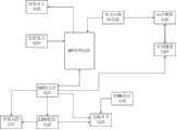
为解决上述技术问题,本发明采用的一个技术方案是:提供了一种耳塞对讲机电路结构,包括MUC主控电路、RF射频电路、发射放大电路、接收放大电路、电源开关电路、LDO稳压电路、USB充电电路、麦克风偏执电路、语音播报电路以及音频播放电路,所述的MUC主控电路、发射放大电路、接收放大电路和麦克风偏执电路均与RF射频电路相连接,所述的MUC主控电路还与电源开关电路、LDO稳压电路音频播放电路和音频播放电路相连接,所述的麦克风偏执电路通过语音播报电路与音频播放电路相连接,所述的电源开关电路与LDO稳压电路和USB充电电路相连接。In order to solve the above-mentioned technical problems, a technical solution adopted in the present invention is: to provide an earplug walkie-talkie circuit structure, including a MUC main control circuit, an RF radio frequency circuit, a transmission amplifier circuit, a reception amplifier circuit, a power switch circuit, and an LDO voltage regulator circuit. , USB charging circuit, microphone bias circuit, voice broadcast circuit and audio playback circuit, the MUC main control circuit, transmitter amplifier circuit, receiver amplifier circuit and microphone bias circuit are all connected with the RF radio frequency circuit, the MUC main control circuit The circuit is also connected with the power switch circuit, the LDO voltage regulator circuit audio playback circuit and the audio playback circuit, the microphone paranoia circuit is connected with the audio playback circuit through the voice broadcast circuit, the power switch circuit is connected with the LDO voltage regulator circuit and the audio playback circuit. connected to the USB charging circuit.
在本发明一个较佳实施例中,所述的MUC主控电路采用20个引脚的IC控制芯片作为主芯片。In a preferred embodiment of the present invention, the MUC main control circuit adopts an IC control chip with 20 pins as the main chip.
在本发明一个较佳实施例中,所述的RF射频电路采用BK4818滤波芯片作为主芯片,并内置26Mhz的高速晶振。In a preferred embodiment of the present invention, the RF radio frequency circuit adopts a BK4818 filter chip as the main chip, and has a built-in high-speed crystal oscillator of 26Mhz.
在本发明一个较佳实施例中,所述的发射放大电路由多个三极管组成电流放大器。In a preferred embodiment of the present invention, the transmit amplifier circuit is composed of a plurality of transistors to form a current amplifier.
在本发明一个较佳实施例中,所述的电源开关电路内置有开关和电池,其中,所述的电池的电压为4.5V。In a preferred embodiment of the present invention, the power switch circuit has a built-in switch and a battery, wherein the voltage of the battery is 4.5V.
在本发明一个较佳实施例中,所述的LDO稳压电路内置有稳压芯片。In a preferred embodiment of the present invention, the LDO voltage regulator circuit has a built-in voltage regulator chip.
在本发明一个较佳实施例中,所述的USB充电电路采用TP4057锂电池充电芯片作为主芯片,并内置有USB接口、红色发光二极管和绿色发光二极管。In a preferred embodiment of the present invention, the USB charging circuit adopts a TP4057 lithium battery charging chip as the main chip, and has a built-in USB interface, red light-emitting diodes and green light-emitting diodes.
在本发明一个较佳实施例中,所述的音频播放电路采用TSSA3159整流芯片和M4890S音频功率放大芯片作为主芯片,并内置有两个扬声器。In a preferred embodiment of the present invention, the audio playback circuit uses a TSSA3159 rectifier chip and an M4890S audio power amplifier chip as the main chip, and has two built-in speakers.
在本发明一个较佳实施例中,所述的耳塞对讲机电路结构还包括按键及指示灯电路,所述的按键及指示灯电路分别与MUC主控电路和LDO稳压电路相连接。In a preferred embodiment of the present invention, the circuit structure of the earplug walkie-talkie further includes a button and an indicator circuit, and the button and indicator circuit are respectively connected to the MUC main control circuit and the LDO voltage regulator circuit.
在本发明一个较佳实施例中,所述的按键及指示灯电路内设置有发光二极管和多个按键开关。In a preferred embodiment of the present invention, a light-emitting diode and a plurality of key switches are arranged in the button and indicator circuit.
本发明的有益效果是:本发明的耳塞对讲机电路结构,增加对讲功能,能够同时防止噪音对耳朵的伤害,还能很清楚的听到对讲的内容,可以进行一对一,一对多和多对多通话,音质清晰,语音传递快,无延迟,超长待机,可以广泛应用于车间现场管理、情侣互动、KTV、餐厅、美容院、餐厅、理发店等场所,应用范围广。The beneficial effects of the present invention are: the circuit structure of the earplug intercom of the present invention increases the intercom function, can simultaneously prevent the damage of noise to the ear, and can clearly hear the content of the intercom, and can carry out one-to-one, one-to-many And many-to-many calls, clear sound quality, fast voice transmission, no delay, long standby, can be widely used in workshop site management, couple interaction, KTV, restaurants, beauty salons, restaurants, barber shops and other places, with a wide range of applications.
附图说明Description of drawings
为了更清楚地说明本发明实施例中的技术方案,下面将对实施例描述中所需要使用的附图作简单地介绍,显而易见地,下面描述中的附图仅仅是本发明的一些实施例,对于本领域普通技术人员来讲,在不付出创造性劳动的前提下,还可以根据这些附图获得其它的附图,其中:In order to illustrate the technical solutions in the embodiments of the present invention more clearly, the following briefly introduces the accompanying drawings used in the description of the embodiments. Obviously, the accompanying drawings in the following description are only some embodiments of the present invention. For those of ordinary skill in the art, under the premise of no creative work, other drawings can also be obtained from these drawings, wherein:
图1 是本发明耳塞对讲机电路结构的一较佳实施例的结构框图;1 is a structural block diagram of a preferred embodiment of the circuit structure of the earplug walkie-talkie of the present invention;
图2是图1中MUC主控电路的电路图;Fig. 2 is the circuit diagram of the MUC main control circuit in Fig. 1;
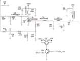
图3是图1中RF射频电路的电路图;Fig. 3 is the circuit diagram of the RF radio frequency circuit in Fig. 1;
图4是图1中发射放大电路的电路图;Fig. 4 is the circuit diagram of the transmitting amplifying circuit in Fig. 1;
图5是图1中接收放大电路的电路图;Fig. 5 is the circuit diagram of the receiving amplifying circuit in Fig. 1;
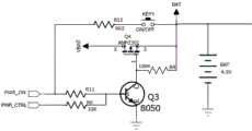
图6是图1中电源开关电路的电路图;Fig. 6 is the circuit diagram of the power switch circuit in Fig. 1;
图7是图1中LDO稳压电路的电路图;Fig. 7 is the circuit diagram of the LDO voltage regulator circuit in Fig. 1;
图8是图1中USB充电电路的电路图;Fig. 8 is the circuit diagram of the USB charging circuit in Fig. 1;
图9是图1中麦克风偏执电路的电路图;Fig. 9 is the circuit diagram of the microphone bias circuit in Fig. 1;
图10是图1中语音播报电路的电路图;Fig. 10 is the circuit diagram of the voice broadcast circuit in Fig. 1;
图11是图1中音频播放电路的电路图;Figure 11 is a circuit diagram of the audio playback circuit in Figure 1;
图12是图1中按键及指示灯电路的电路图。FIG. 12 is a circuit diagram of the button and indicator circuit in FIG. 1 .
具体实施方式Detailed ways
下面将对本发明实施例中的技术方案进行清楚、完整地描述,显然,所描述的实施例仅是本发明的一部分实施例,而不是全部的实施例。基于本发明中的实施例,本领域普通技术人员在没有做出创造性劳动前提下所获得的所有其它实施例,都属于本发明保护的范围。The technical solutions in the embodiments of the present invention will be clearly and completely described below. Obviously, the described embodiments are only a part of the embodiments of the present invention, rather than all the embodiments. Based on the embodiments of the present invention, all other embodiments obtained by those of ordinary skill in the art without creative efforts shall fall within the protection scope of the present invention.
如图1所示,本发明实施例包括:As shown in FIG. 1, the embodiment of the present invention includes:
一种耳塞对讲机电路结构,包括MUC主控电路、RF射频电路、发射放大电路、接收放大电路、电源开关电路、LDO稳压电路、USB充电电路、麦克风偏执电路、语音播报电路以及音频播放电路,所述的MUC主控电路、发射放大电路、接收放大电路和麦克风偏执电路均与RF射频电路相连接,所述的MUC主控电路还与电源开关电路、LDO稳压电路音频播放电路和音频播放电路相连接,所述的麦克风偏执电路通过语音播报电路与音频播放电路相连接,所述的电源开关电路与LDO稳压电路和USB充电电路相连接。An earplug walkie-talkie circuit structure, comprising a MUC main control circuit, an RF radio frequency circuit, a transmission amplifier circuit, a reception amplifier circuit, a power switch circuit, an LDO voltage regulator circuit, a USB charging circuit, a microphone bias circuit, a voice broadcast circuit and an audio playback circuit, The MUC main control circuit, the transmitting amplifier circuit, the receiving amplifier circuit and the microphone bias circuit are all connected with the RF radio frequency circuit, and the MUC main control circuit is also connected with the power switch circuit, the LDO voltage regulator circuit, the audio playback circuit and the audio playback circuit The microphone bias circuit is connected with the audio playback circuit through the voice broadcast circuit, and the power switch circuit is connected with the LDO voltage regulator circuit and the USB charging circuit.
上述中,所述的MUC主控电路采用20个引脚的IC控制芯片作为主芯片,由MUC主控电路控制各个电路的运行状态。In the above, the MUC main control circuit uses a 20-pin IC control chip as the main chip, and the MUC main control circuit controls the operation status of each circuit.
其中,所述的RF射频电路采用32个引脚的BK4818滤波芯片作为主芯片,并内置26Mhz的高速晶振,由RF射频电路和麦克风偏执电路达到了很好降噪效果,音质清晰, 能够同时防止噪音对耳朵的伤害,还能很清楚的听到对讲的内容。Among them, the RF radio frequency circuit uses a 32-pin BK4818 filter chip as the main chip, and has a built-in 26Mhz high-speed crystal oscillator. The RF radio frequency circuit and the microphone bias circuit achieve a good noise reduction effect, the sound quality is clear, and it can prevent Noise damages the ears, and the content of the intercom can be clearly heard.
所述的发射放大电路由多个三极管组成电流放大器,由接收放大电路和发射放大电路对接收和发射的电流信号进行放大处理,能够发出清晰的声音以及清楚的听到对讲的内容,提高语音对话的质量。The transmitting amplifying circuit is composed of a plurality of transistors to form a current amplifier, and the receiving and transmitting amplifying circuit amplifies the received and transmitted current signals, which can produce clear voices and clearly hear the content of the intercom, and improve the voice. the quality of the conversation.
本实施例中,所述的电源开关电路内置有开关和电池,其中,所述的电池的电压为4.5V,由电源开关电路给整个耳塞对讲机提供供电。所述的LDO稳压电路内置有5个引脚的稳压芯片,由LDO稳压电路控制电源的稳定性。In this embodiment, the power switch circuit has a built-in switch and a battery, wherein the voltage of the battery is 4.5V, and the power switch circuit provides power to the entire earplug walkie-talkie. The LDO voltage stabilizer circuit has a built-in voltage stabilizer chip with 5 pins, and the stability of the power supply is controlled by the LDO voltage stabilizer circuit.
进一步的,所述的USB充电电路采用6个引脚的TP4057锂电池充电芯片作为主芯片,并内置有USB接口、红色发光二极管和绿色发光二极管。电源开关电路还可以通过USB充电电路提供电源,所述的USB接口与TP4057锂电池充电芯片相连接给TP4057锂电池充电芯片进行充电处理,由USB充电电路采用USB充电接口的设计,即使充电器丢失,也能轻松充电,充电器/电脑/充电宝/车载多种充电方式,更快更方便。Further, the USB charging circuit adopts a 6-pin TP4057 lithium battery charging chip as the main chip, and has a built-in USB interface, a red light-emitting diode and a green light-emitting diode. The power switch circuit can also provide power through the USB charging circuit. The USB interface is connected to the TP4057 lithium battery charging chip to charge the TP4057 lithium battery charging chip. The USB charging circuit adopts the design of the USB charging interface, even if the charger is lost. , It can also be easily charged, with a variety of charging methods for charger/computer/charging treasure/car, which is faster and more convenient.
其中,所述的音频播放电路采用6个引脚的TSSA3159整流芯片和8个引脚的M4890S音频功率放大芯片作为主芯片,并内置有两个扬声器,能够发出清晰的声音。Among them, the audio playback circuit uses a 6-pin TSSA3159 rectifier chip and an 8-pin M4890S audio power amplifier chip as the main chip, and has two built-in speakers, which can emit clear sound.
再进一步的,所述的耳塞对讲机电路结构还包括按键及指示灯电路,所述的按键及指示灯电路分别与MUC主控电路和LDO稳压电路相连接。其中,所述的按键及指示灯电路内设置有发光二极管和多个按键开关,多个按键开关包括休眠按钮、音量调节器、频率调节器,控制部分均是通过多个按键实现所有控制功能,用于控制操作整个耳塞对讲机的使用。Still further, the circuit structure of the earplug walkie-talkie further includes a button and an indicator circuit, and the button and indicator circuit are respectively connected with the MUC main control circuit and the LDO voltage regulator circuit. Among them, the key and indicator circuit are provided with light-emitting diodes and a plurality of key switches, and the plurality of key switches include a sleep button, a volume regulator, and a frequency regulator, and the control part realizes all control functions through a plurality of keys. Used to control the operation of the entire earbud walkie-talkie.
具体的,所述的MUC主控电路中IC控制芯片的第17、16、和15引脚分别与RF射频电路中BK4818滤波芯片的第25、26和27引脚相连接;所述的发射放大电路与RF射频电路中BK4818滤波芯片的第17引脚相连接;所述的接收放大电路与RF射频电路中BK4818滤波芯片的第15引脚相连接;所述的电源开关电路与USB充电电路中TP4057锂电池充电芯片的第3引脚相连接;所述的麦克风偏执电路与RF射频电路中BK4818滤波芯片的第13引脚相连接。Specifically, the 17th, 16th, and 15th pins of the IC control chip in the MUC main control circuit are respectively connected with the 25th, 26th, and 27th pins of the BK4818 filter chip in the RF radio frequency circuit; the transmission amplifier The circuit is connected with the 17th pin of the BK4818 filter chip in the RF radio frequency circuit; the receiving amplifier circuit is connected with the 15th pin of the BK4818 filter chip in the RF radio frequency circuit; the power switch circuit is connected with the USB charging circuit. The third pin of the TP4057 lithium battery charging chip is connected; the microphone bias circuit is connected with the 13th pin of the BK4818 filter chip in the RF radio frequency circuit.
实施例:Example:
如图2所示,所述的MUC主控电路包括IC控制芯片U7、第十四电容C14、第十五电容C15、第四十五电容C45和第二电阻R2,所述的第十四电容C14、第十五电容C15、第四十五电容C46分别与IC控制芯片U7的引脚并联连接,所述的第二电阻R2与与IC控制芯片U7的引脚串联连接,其中,所述的第十四电容C14和第十五电容C15还进行接地连接。As shown in FIG. 2, the MUC main control circuit includes an IC control chip U7, a fourteenth capacitor C14, a fifteenth capacitor C15, a forty-fifth capacitor C45 and a second resistor R2. The fourteenth capacitor C14, the fifteenth capacitor C15, and the forty-fifth capacitor C46 are respectively connected in parallel with the pins of the IC control chip U7, and the second resistor R2 is connected in series with the pins of the IC control chip U7, wherein the The fourteenth capacitor C14 and the fifteenth capacitor C15 are also connected to ground.
如图3所示,所述的RF射频电路包括BK4818滤波芯片U4、高速晶振X1、第二电容C2、第六电容C6、第九电容C9、第十三电容C13、第十六电容C16、第十九电容C19、第二十一电容C21、第二十二电容C22、第二十五电容C25、第二十六电容C26、第二十七电容C27、第三十五电容C35、第四十一电容C41、第四十四电容C44、第五十二电容C52、第九电阻R9、第十五电阻R15、第二十四电阻R14、第三十三电阻R33和第三十五电阻R35,所述的第六电容C6、第十三电容C13、第二十一电容C21、第二十六电容C26、第二十七电容C27、第五十二电容C52和第三十五电阻R35分别与BK4818滤波芯片U4串联连接,所述的第二电容C2、第六电容C6、第九电容C9、第十九电容C19、第二十二电容C22、第二十五电容C25、第四十一电容C41、第四十三电容C43、第四十四电容C44和第三十三电阻R33分别与BK4818滤波芯片U4并联连接,所述的第五十二电容C52和第九电阻R9还与高速晶振X1串联连接,所述的第十五电阻R15、第二十四电阻R24和第三十五电阻R35分别与高速晶振X1并联连接,其中,所述的第二电容C2、第六电容C6、第九电容C9、第十三电容C13、第十九电容C19、第二十二电容C22、第二十五电容C25、第二十七电容C27、第三十五电容C35、第四十一电容C41、第四十三电容C43和第四十四电容C44均进行接地连接。As shown in Figure 3, the RF circuit includes a BK4818 filter chip U4, a high-speed crystal oscillator X1, a second capacitor C2, a sixth capacitor C6, a ninth capacitor C9, a thirteenth capacitor C13, a sixteenth capacitor C16, and a sixth capacitor C6. The nineteenth capacitor C19, the twenty-first capacitor C21, the twenty-second capacitor C22, the twenty-fifth capacitor C25, the twenty-sixth capacitor C26, the twenty-seventh capacitor C27, the thirty-fifth capacitor C35, the fortieth capacitor A capacitor C41, the forty-fourth capacitor C44, the fifty-second capacitor C52, the ninth resistor R9, the fifteenth resistor R15, the twenty-fourth resistor R14, the thirty-third resistor R33 and the thirty-fifth resistor R35, The sixth capacitor C6, the thirteenth capacitor C13, the twenty-first capacitor C21, the twenty-sixth capacitor C26, the twenty-seventh capacitor C27, the fifty-second capacitor C52 and the thirty-fifth resistor R35 are respectively connected with The BK4818 filter chip U4 is connected in series, the second capacitor C2, the sixth capacitor C6, the ninth capacitor C9, the nineteenth capacitor C19, the twenty-second capacitor C22, the twenty-fifth capacitor C25, and the forty-first capacitor C41, the forty-third capacitor C43, the forty-fourth capacitor C44 and the thirty-third resistor R33 are respectively connected in parallel with the BK4818 filter chip U4. The fifty-second capacitor C52 and the ninth resistor R9 are also connected to the high-speed crystal oscillator X1 connected in series, the fifteenth resistor R15, the twenty-fourth resistor R24 and the thirty-fifth resistor R35 are respectively connected in parallel with the high-speed crystal oscillator X1, wherein the second capacitor C2, the sixth capacitor C6, the ninth capacitor Capacitor C9, thirteenth capacitor C13, nineteenth capacitor C19, twenty-second capacitor C22, twenty-fifth capacitor C25, twenty-seventh capacitor C27, thirty-fifth capacitor C35, forty-first capacitor C41, The forty-third capacitor C43 and the forty-fourth capacitor C44 are both grounded.
如图4所示,所述的发射放大电路包括第一三极管Q1、第五三极管Q5、第六三极管Q6、第八电容C8、第十八电容C18、第二十八电容C28、第二十九电容C29、第三十七电容C37、第三十八电容C38、第四十电容C44、第四十二电容C42、第四十七电容C47、第四十九电容C49、第五十电容C50、第五十一电容C51、第二十电阻R20、第二十一电阻R21、第二十三电阻R23、第三十电阻R30、第一电感L1、第三电感L3、第五电感L5和第七电感L7,所述的第五三极管Q5的基极与第六三极Q6管的集电极相连接,所述的第八电容C8、第一电感L1和第五电感L5与第一三极管Q1的基极串联连接,所述的第三电感L3、第十八电容C18和第四十电容C40与第一三极管Q1的基极并联连接,所述的第七电感L7与第一三极管Q1的发射极串联连接,所述的第三十七电容C37和第三十八电容C38与第一三极管Q1的发射极并联连接,所述的第九电感R9、第四十七电容C47、第三十电阻R30、第二十三电阻R23和第二十电阻R20连接在第一三极管Q1的发射极和基极之间,所述的第二十八电容C28、第四十二电容C42、第五十电容C50、第五十一电容C51和第二十一电阻R21分别并联连接在第一三极管Q1的发射极和基极之间,所述的第四十九电容C49和第三电感L3并联连接,所述的第二十九电容C29与第四十七电容C47并联连接,其中,所述的第十八电容C18、第二十八电容C28、第二十九电容C29、第三十七电容C37、第四十电容C40、第四十二电容C42、第四十九电容C49、第五十电容C50、第五十一电容C51、第二十一电阻R21、第一三极管Q1的集电极和第六三极管Q6的发射极均进行接地连接。As shown in FIG. 4 , the emission amplifier circuit includes a first transistor Q1, a fifth transistor Q5, a sixth transistor Q6, an eighth capacitor C8, an eighteenth capacitor C18, and a twenty-eighth capacitor C28, the twenty-ninth capacitor C29, the thirty-seventh capacitor C37, the thirty-eighth capacitor C38, the fortieth capacitor C44, the forty-second capacitor C42, the forty-seventh capacitor C47, the forty-ninth capacitor C49, The fiftieth capacitor C50, the fifty-first capacitor C51, the twentieth resistor R20, the twenty-first resistor R21, the twenty-third resistor R23, the thirtieth resistor R30, the first inductor L1, the third inductor L3, the The fifth inductor L5 and the seventh inductor L7, the base of the fifth transistor Q5 is connected to the collector of the sixth transistor Q6, the eighth capacitor C8, the first inductor L1 and the fifth inductor L5 is connected in series with the base of the first transistor Q1, the third inductor L3, the eighteenth capacitor C18 and the fortieth capacitor C40 are connected in parallel with the base of the first transistor Q1, and the third The seven inductors L7 are connected in series with the emitter of the first transistor Q1, the thirty-seventh capacitor C37 and the thirty-eighth capacitor C38 are connected in parallel with the emitter of the first transistor Q1, and the ninth capacitor C38 is connected in parallel with the emitter of the first transistor Q1. The inductor R9, the forty-seventh capacitor C47, the thirtieth resistor R30, the twenty-third resistor R23 and the twentieth resistor R20 are connected between the emitter and the base of the first transistor Q1, and the second The eighteenth capacitor C28, the forty-second capacitor C42, the fifty-first capacitor C50, the fifty-first capacitor C51 and the twenty-first resistor R21 are respectively connected in parallel between the emitter and the base of the first transistor Q1, The forty-ninth capacitor C49 is connected in parallel with the third inductor L3, the twenty-ninth capacitor C29 is connected in parallel with the forty-seventh capacitor C47, wherein the eighteenth capacitor C18, the twenty-ninth capacitor The eighth capacitor C28, the twenty-ninth capacitor C29, the thirty-seventh capacitor C37, the fortieth capacitor C40, the forty-second capacitor C42, the forty-ninth capacitor C49, the fifty-first capacitor C50, and the fifty-first capacitor C51 , the twenty-first resistor R21, the collector of the first transistor Q1 and the emitter of the sixth transistor Q6 are all connected to ground.
如图5所示,所述的接收放大电路包括第二三极管Q2、二极管D1、第三十一电容C31、第五十三电容C53、第六十电容C60、第六十一电容C61、第六十二电容C62、第六十三电容C63、第六十四电容C64、第六十五电容C65、第六十六电容C66、第八电阻R8、第六电感L6、第八电感L8、第十电感L10、第十一电感L11和第十二电感L12,所述的第二三极管Q2、二极管D1、第六十三电容C63、第六十六电容C66、第二十五电阻R25、第六电感L6、第八电感L8、第十电感L10和第十二电感L12均并联连接,所述的第六十一电容C61连接在第六十三电容C63和第六电感L6之间,所述的第六十二电容C62连接在第六电感L6与第二十五电阻R25之间,所述的第五十三电容C53连接在第六十六电容C66与第十二电感L12之间,所述的第二十电容C20连接在第十二电感L12与第八电感L8之间,所述的第六十电容C60连接在第八电感L8与第十电感L10之间,所述的第六十四电容C64和第十二电感L12串联连接,所述的第六十五电容C65与和第八电感L8串联连接,所述的第二三极管Q2的集电极还与第十一电感L11串联连接,所述的第三十一电容C31与第十一电感L11并联连接,所述的第八电阻R8连接在第二三极管Q2的基极与集电极之间,所述的第二十五电阻R25与第二三极管Q2的基极相连接,其中,所述的第三十一电容C31、第六十三电容C63、第六十四电容C64、第六十五电容C65、第六十六电容C66、第二十五电阻R25、第六电感L6、第十电感L10、二极管D1和第二三极管Q2的发射极均进行接地连接。As shown in FIG. 5 , the receiving amplifier circuit includes a second transistor Q2, a diode D1, a thirty-first capacitor C31, a fifty-third capacitor C53, a sixtieth capacitor C60, a sixty-first capacitor C61, The sixty-second capacitor C62, the sixty-third capacitor C63, the sixty-fourth capacitor C64, the sixty-fifth capacitor C65, the sixty-sixth capacitor C66, the eighth resistor R8, the sixth inductor L6, the eighth inductor L8, The tenth inductance L10, the eleventh inductance L11 and the twelfth inductance L12, the second transistor Q2, the diode D1, the sixty-third capacitor C63, the sixty-sixth capacitor C66, and the twenty-fifth resistor R25 , the sixth inductor L6, the eighth inductor L8, the tenth inductor L10 and the twelfth inductor L12 are all connected in parallel, and the sixty-first capacitor C61 is connected between the sixty-third capacitor C63 and the sixth inductor L6, The sixty-second capacitor C62 is connected between the sixth inductor L6 and the twenty-fifth resistor R25, and the fifty-third capacitor C53 is connected between the sixty-sixth capacitor C66 and the twelfth inductor L12 , the twentieth capacitor C20 is connected between the twelfth inductor L12 and the eighth inductor L8, the sixtieth capacitor C60 is connected between the eighth inductor L8 and the tenth inductor L10, the The sixty-fourth capacitor C64 is connected in series with the twelfth inductor L12, the sixty-fifth capacitor C65 is connected in series with the eighth inductor L8, and the collector of the second transistor Q2 is also connected with the eleventh inductor. L11 is connected in series, the thirty-first capacitor C31 is connected in parallel with the eleventh inductor L11, the eighth resistor R8 is connected between the base and the collector of the second transistor Q2, and the first The twenty-fifth resistor R25 is connected to the base of the second transistor Q2, wherein the thirty-first capacitor C31, the sixty-third capacitor C63, the sixty-fourth capacitor C64, and the sixty-fifth capacitor C65 , the sixty-sixth capacitor C66, the twenty-fifth resistor R25, the sixth inductor L6, the tenth inductor L10, the diode D1 and the emitters of the second transistor Q2 are all connected to ground.
如图6所示,所述的电源开关电路包括第三三极管Q3、第四三极管Q4、第四电阻R4、第六电阻R6、第十一电阻R11、第十二电阻R12、第一开关KEY1和电池BAT,所述的第六电阻R6和第十一电阻R11并联连接在第三三极管Q3的基极,所述的第四三极管Q4和第四电阻R4并联连接在第三三极管Q3的集电极,所述的第十二电阻R12和第一开关KEY1串联连接在第三三极管Q3基极和集电极之间,所述的电池BAT与第三三极管Q3的集电极相连接,其中,所述的第三三极管Q3的发射极和电池BAT均进行接地连接。As shown in FIG. 6 , the power switch circuit includes a third transistor Q3, a fourth transistor Q4, a fourth resistor R4, a sixth resistor R6, an eleventh resistor R11, a twelfth resistor R12, A switch KEY1 and a battery BAT, the sixth resistor R6 and the eleventh resistor R11 are connected in parallel to the base of the third transistor Q3, and the fourth transistor Q4 and the fourth resistor R4 are connected in parallel to The collector of the third transistor Q3, the twelfth resistor R12 and the first switch KEY1 are connected in series between the base and the collector of the third transistor Q3, the battery BAT and the third transistor The collector of the transistor Q3 is connected to each other, wherein the emitter of the third transistor Q3 and the battery BAT are both grounded.
如图7所示,所述的电源开关电路包括稳压芯片U3、第一电容C1、第三电容C3、第十二电容C12、第四十八电容C48、第一电阻R1和第二十二电阻R22,所述的第一电容C1、第一电阻R1和第二十二电阻R22均与稳压芯片U3串联连接,所述的第十二电容C12并联在第一电容C1和稳压芯片U3之间,所述的第三电容C3并联在第一电阻R1和稳压芯片U3之间,所述的第四十八电容C48与第二十二电阻R22并联连接,其中,所述的稳压芯片U3、第一电容C1、第三电容C3、第十二电容C12、第四十八电容C48和第二十二电阻R22均进行接地连接。As shown in FIG. 7 , the power switch circuit includes a voltage regulator chip U3, a first capacitor C1, a third capacitor C3, a twelfth capacitor C12, a forty-eighth capacitor C48, a first resistor R1 and a twenty-second capacitor Resistor R22, the first capacitor C1, the first resistor R1 and the twenty-second resistor R22 are all connected in series with the voltage regulator chip U3, and the twelfth capacitor C12 is connected in parallel with the first capacitor C1 and the voltage regulator chip U3 between, the third capacitor C3 is connected in parallel between the first resistor R1 and the voltage regulator chip U3, the forty-eighth capacitor C48 is connected in parallel with the twenty-second resistor R22, wherein the voltage regulator The chip U3, the first capacitor C1, the third capacitor C3, the twelfth capacitor C12, the forty-eighth capacitor C48 and the twenty-second resistor R22 are all connected to ground.
如图8所示,所述的USB充电电路包括锂电池充电芯片U1、USB接口USB1、第四十六电容C46、第三十一电阻R31、第三十四电阻R34、第三十六电阻R36、第三发光二极管LED3和第四发光二极管LED4,所述的USB接口USB1、第四十六电容C46、第三十四电阻R34均与锂电池充电芯片U1相连接,所述的第三发光二极管LED3和第三十一电阻R31串联连接后与锂电池充电芯片U1相连接,所述的第四发光二极管LED4和第三十六电阻R36串联连接后与锂电池充电芯片U1相连接,其中,所述的USB接口USB1、第四十六电容C46和第三十四电阻R34均进行接地连接。As shown in FIG. 8 , the USB charging circuit includes a lithium battery charging chip U1, a USB interface USB1, a forty-sixth capacitor C46, a thirty-first resistor R31, a thirty-fourth resistor R34, and a thirty-sixth resistor R36 , the third light-emitting diode LED3 and the fourth light-emitting diode LED4, the USB interface USB1, the forty-sixth capacitor C46, and the thirty-fourth resistor R34 are all connected to the lithium battery charging chip U1, and the third light-emitting diode The LED3 and the thirty-first resistor R31 are connected in series to the lithium battery charging chip U1, and the fourth light-emitting diode LED4 and the thirty-sixth resistor R36 are connected in series to the lithium battery charging chip U1. The USB interface USB1, the forty-sixth capacitor C46 and the thirty-fourth resistor R34 are all grounded.
如图9所示,所述的麦克风偏执电路包括麦克风MIC1、第二十三电容C23、第三十电容C30、第五电阻R5和第七电阻R7,所述的第五电阻R5和第七电阻R7串联后与麦克风MIC1并联连接,所述的第三十电容C30并联连接在第五电阻R5和第七电阻R7之间,所述的第二十三电容C23与麦克风MIC1并联连接,其中,所述的第二十三电容C23、第三十电容C30和麦克风MIC1均进行接地连接。As shown in FIG. 9 , the microphone bias circuit includes a microphone MIC1, a twenty-third capacitor C23, a thirtieth capacitor C30, a fifth resistor R5 and a seventh resistor R7, and the fifth resistor R5 and the seventh resistor R7 is connected in parallel with the microphone MIC1 after being connected in series, the thirtieth capacitor C30 is connected in parallel between the fifth resistor R5 and the seventh resistor R7, and the twenty-third capacitor C23 is connected in parallel with the microphone MIC1, wherein all the The twenty-third capacitor C23, the thirtieth capacitor C30 and the microphone MIC1 are all grounded.
如图10所示,所述的语音播报电路包括语音芯片U8、第四电容C4、第六十七电容C67、第十八电阻R18、第二十六电阻R26、第二十八电阻R28、第三十七电阻R37和第三十八电阻R38,所述的第六十七电容C67和第二十六电阻R26串联连接后与语音芯片U8相连接,所述的第三十七电阻R37和第二十八电阻R28串联连接后与语音芯片U8相连接,所述的第四电容C4并联连接在第二十八电阻R28和第三十七电阻R37之间,所述的第二十六电阻R26和第三十八电阻R38均与语音芯片U8并联连接,其中,所述的第三十八电阻R38进行接地连接。As shown in Figure 10, the voice broadcast circuit includes a voice chip U8, a fourth capacitor C4, a sixty-seventh capacitor C67, an eighteenth resistor R18, a twenty-sixth resistor R26, a twenty-eighth resistor R28, The thirty-seventh resistor R37 and the thirty-eighth resistor R38, the sixty-seventh capacitor C67 and the twenty-sixth resistor R26 are connected in series and connected to the voice chip U8, the thirty-seventh resistor R37 and the third The twenty-eighth resistor R28 is connected in series with the voice chip U8, the fourth capacitor C4 is connected in parallel between the twenty-eighth resistor R28 and the thirty-seventh resistor R37, and the twenty-sixth resistor R26 and the thirty-eighth resistor R38 are connected in parallel with the voice chip U8, wherein the thirty-eighth resistor R38 is connected to ground.
如图11所示,所述的音频播放电路包括第一扬声器SPK1、第二扬声器SPK2、整流芯片U5、音频功率放大芯片U2、第五电容C5、第七电容C7、第十电容C10、第十一电容C11、第二十四电容C24、第三十二电容C32、第三十三电容C33、第三电阻R3、第十电阻R10、第十四电阻R14和第三十二电阻R32,所述的第十四电阻R14和第三十二电阻R32与整流芯片U5相连接,所述的整流芯片U5通过第二十四电容C24和第十电阻R10与音频功率放大芯片U2相连接,所述的音频功率放大芯片U2分别与第一扬声器SPK1、第五电容C5、第三十二电容C32相连接,所述的第三电阻R3、第十电容C10和第十一电容C11与音频功率放大芯片U2并联连接,所述的第七电容C7与第三电阻R3并联连接,所述的第三十三电容C33与第三十二电容C32并联连接,所述的第二扬声器SPK2与第一扬声器SPK1并联连接,其中,所述的第五电容C5、第十电容C10、第十一电容C11、第三十二电容C32和第三十三电容C33均进行接地连接。As shown in FIG. 11, the audio playback circuit includes a first speaker SPK1, a second speaker SPK2, a rectifier chip U5, an audio power amplifier chip U2, a fifth capacitor C5, a seventh capacitor C7, a tenth capacitor C10, a tenth capacitor A capacitor C11, a twenty-fourth capacitor C24, a thirty-second capacitor C32, a thirty-third capacitor C33, a third resistor R3, a tenth resistor R10, a fourteenth resistor R14 and a thirty-second resistor R32, the The fourteenth resistor R14 and the thirty-second resistor R32 are connected to the rectifier chip U5, and the rectifier chip U5 is connected to the audio power amplifier chip U2 through the twenty-fourth capacitor C24 and the tenth resistor R10. The audio power amplifier chip U2 is respectively connected with the first speaker SPK1, the fifth capacitor C5, and the thirty-second capacitor C32, and the third resistor R3, the tenth capacitor C10 and the eleventh capacitor C11 are connected with the audio power amplifier chip U2 connected in parallel, the seventh capacitor C7 is connected in parallel with the third resistor R3, the thirty-third capacitor C33 is connected in parallel with the thirty-second capacitor C32, and the second speaker SPK2 is connected in parallel with the first speaker SPK1 connection, wherein the fifth capacitor C5, the tenth capacitor C10, the eleventh capacitor C11, the thirty-second capacitor C32 and the thirty-third capacitor C33 are all connected to ground.
如图12所示,所述的按键及指示灯电路,其中,按键电路包括第二开关、第三开关和第四开关,所述的第二开关、第三开关和第四开关并联连接后载进行接地连接;所述的指示灯电路包括第一发光二极管LED1和第十七电阻R17,所述的第一发光二极管LED1和第十七电阻R17串联连接在一起。As shown in FIG. 12 , in the button and indicator light circuit, the button circuit includes a second switch, a third switch and a fourth switch, and the second switch, the third switch and the fourth switch are connected in parallel to load Make a ground connection; the indicator circuit includes a first light emitting diode LED1 and a seventeenth resistor R17, and the first light emitting diode LED1 and the seventeenth resistor R17 are connected together in series.
通过耳塞对讲机电路所制成的耳塞对讲机轻盈,是一款工厂车间实用型耳塞,又是一种双向移动通信工具,在不需要任何网络支持的情况下,就可以通话,没有话费产生,适用于相对固定且频繁通话的场合。对于生产车间,相对原本耳塞,喊话器,使用起来有局限性,分贝大的场所,很难做到降音并且能让对方知道自己的意图,而耳塞对讲机却能做到防噪音,而且还能够清楚的通过对讲来传递所需要的信息。The earplug walkie-talkie made by the earplug walkie-talkie circuit is light, it is a practical earplug in the factory workshop, and it is also a two-way mobile communication tool. Relatively fixed and frequent call occasions. For the production workshop, compared with the original earplugs and megaphones, there are limitations in use. In places with large decibels, it is difficult to reduce the sound and let the other party know their intentions, while the earplug walkie-talkies can prevent noise, and can also Clearly communicate the required information through the intercom.
通过耳塞对讲机电路所制成的耳塞对讲机的功能:The function of the earphone walkie-talkie made by the earphone walkie-talkie circuit:
1.降噪型耳塞1. Noise-cancelling earplugs
在噪音大的环境下 ,可以起来防噪音效果;In a noisy environment, the anti-noise effect can be achieved;
2.实时对讲2. Real-time intercom
可以进行一对一,一对多和多对多通话,音质清晰,语音传递快,无延迟;One-to-one, one-to-many and many-to-many calls are possible, with clear sound quality, fast voice transmission, and no delay;
3.休眠按钮(TOANY-8000独有功能)3. Sleep button (TOANY-8000 unique function)
如果你不想接收受话的话,可以按下sleep按键,就可以拒绝收听任何语音,如果你想再次接收受话的话,再按一下此键就可以了;If you don't want to receive the incoming call, you can press the sleep button, you can refuse to listen to any voice, if you want to receive the incoming call again, press this button again;
4.音量 6 级调节4. 6-level volume adjustment
音量可以6级调节,任意选择适合的音量即可。The volume can be adjusted in 6 levels, and you can choose the appropriate volume arbitrarily.
综上所述,本发明的耳塞对讲机电路结构,增加对讲功能,能够同时防止噪音对耳朵的伤害,还能很清楚的听到对讲的内容,可以进行一对一,一对多和多对多通话,音质清晰,语音传递快,无延迟,超长待机,可以广泛应用于车间现场管理、情侣互动、KTV、餐厅、美容院、餐厅、理发店等场所,应用范围广。To sum up, the circuit structure of the earplug walkie-talkie of the present invention increases the intercom function, can prevent the damage of noise to the ear at the same time, and can clearly hear the content of the intercom, and can carry out one-to-one, one-to-many and multiple For multiple calls, the sound quality is clear, the voice transmission is fast, no delay, and long standby time. It can be widely used in workshop site management, couple interaction, KTV, restaurants, beauty salons, restaurants, barber shops and other places, with a wide range of applications.
以上所述仅为本发明的实施例,并非因此限制本发明的专利范围,凡是利用本发明说明书内容所作的等效结构或等效流程变换,或直接或间接运用在其它相关的技术领域,均同理包括在本发明的专利保护范围内。The above descriptions are only the embodiments of the present invention, and are not intended to limit the scope of the patent of the present invention. Any equivalent structure or equivalent process transformation made by using the contents of the description of the present invention, or directly or indirectly applied in other related technical fields, are all applicable. Similarly, it is included in the scope of patent protection of the present invention.
Claims (10)
Priority Applications (1)
| Application Number | Priority Date | Filing Date | Title |
|---|---|---|---|
| CN201910914280.XACN110784238A (en) | 2019-09-26 | 2019-09-26 | An earplug walkie-talkie circuit structure |
Applications Claiming Priority (1)
| Application Number | Priority Date | Filing Date | Title |
|---|---|---|---|
| CN201910914280.XACN110784238A (en) | 2019-09-26 | 2019-09-26 | An earplug walkie-talkie circuit structure |
Publications (1)
| Publication Number | Publication Date |
|---|---|
| CN110784238Atrue CN110784238A (en) | 2020-02-11 |
Family
ID=69384431
Family Applications (1)
| Application Number | Title | Priority Date | Filing Date |
|---|---|---|---|
| CN201910914280.XAPendingCN110784238A (en) | 2019-09-26 | 2019-09-26 | An earplug walkie-talkie circuit structure |
Country Status (1)
| Country | Link |
|---|---|
| CN (1) | CN110784238A (en) |
Citations (6)
| Publication number | Priority date | Publication date | Assignee | Title |
|---|---|---|---|---|
| CN203691470U (en)* | 2014-01-24 | 2014-07-02 | 安徽太一通信科技有限公司 | Ear-hanging type digital interphone |
| WO2018107673A1 (en)* | 2016-12-12 | 2018-06-21 | 深圳佳比泰智能照明股份有限公司 | Frequency-modulated transmitting circuit and frequency-modulated transmitting method |
| CN108769872A (en)* | 2018-06-29 | 2018-11-06 | 江西联创宏声电子股份有限公司 | Earphone Dolby circuit |
| CN209330109U (en)* | 2019-02-25 | 2019-08-30 | 董全 | Wearable intercom and intercom system |
| CN110266337A (en)* | 2019-07-24 | 2019-09-20 | 常熟市欧伏罱电子有限公司 | A kind of mini earplug intercom |
| CN210536624U (en)* | 2019-09-26 | 2020-05-15 | 常熟市欧伏罱电子有限公司 | Circuit structure of earplug interphone |
- 2019
- 2019-09-26CNCN201910914280.XApatent/CN110784238A/enactivePending
Patent Citations (6)
| Publication number | Priority date | Publication date | Assignee | Title |
|---|---|---|---|---|
| CN203691470U (en)* | 2014-01-24 | 2014-07-02 | 安徽太一通信科技有限公司 | Ear-hanging type digital interphone |
| WO2018107673A1 (en)* | 2016-12-12 | 2018-06-21 | 深圳佳比泰智能照明股份有限公司 | Frequency-modulated transmitting circuit and frequency-modulated transmitting method |
| CN108769872A (en)* | 2018-06-29 | 2018-11-06 | 江西联创宏声电子股份有限公司 | Earphone Dolby circuit |
| CN209330109U (en)* | 2019-02-25 | 2019-08-30 | 董全 | Wearable intercom and intercom system |
| CN110266337A (en)* | 2019-07-24 | 2019-09-20 | 常熟市欧伏罱电子有限公司 | A kind of mini earplug intercom |
| CN210536624U (en)* | 2019-09-26 | 2020-05-15 | 常熟市欧伏罱电子有限公司 | Circuit structure of earplug interphone |
Similar Documents
| Publication | Publication Date | Title |
|---|---|---|
| CN203243413U (en) | Anti-eavesdropping and recording blocker device | |
| CN101170325A (en) | bluetooth wireless microphone | |
| CN210536624U (en) | Circuit structure of earplug interphone | |
| CN110784238A (en) | An earplug walkie-talkie circuit structure | |
| CN205812305U (en) | A kind of intelligent radio microphone | |
| CN217116345U (en) | A multifunctional expansion PCBA mainboard for earphones and earphones | |
| CN201054596Y (en) | Automatic detection device for Bluetooth frequency modulation transmission band port | |
| CN206149261U (en) | Changeable audio equipment of wireless receiving and dispatching | |
| CN212519363U (en) | A kind of intelligent sensing outside sound type earphone | |
| CN215345007U (en) | Stereo wireless Bluetooth headset control circuit and device | |
| CN207589153U (en) | A kind of audio system using S08 sound card converters | |
| CN206149269U (en) | Bluetooth device with variable communication range and Bluetooth speaker | |
| CN201039240Y (en) | Radio mouse call system | |
| CN206251282U (en) | A kind of studio broadcast intercom | |
| CN208210221U (en) | Realize the performance device around audio | |
| CN217335860U (en) | Multifunctional ENC communication noise reduction earphone | |
| CN207488984U (en) | A kind of S08 sound card converters for supporting portable computer | |
| CN207720396U (en) | Mobile phone USB sound cards | |
| CN111836155A (en) | Headphone with automatic volume adjustment function and volume adjustment method | |
| CN205883507U (en) | Smart broadcast bluetooth headset | |
| CN221263878U (en) | Multifunctional interview live broadcast system | |
| CN204836469U (en) | Bluetooth microphone | |
| CN206258583U (en) | Integrated voice module and its application system based on big-dipper satellite | |
| CN205961410U (en) | Audio ware | |
| CN204350099U (en) | A kind of communication system for GSM-R hand-held station |
Legal Events
| Date | Code | Title | Description |
|---|---|---|---|
| PB01 | Publication | ||
| PB01 | Publication | ||
| SE01 | Entry into force of request for substantive examination | ||
| SE01 | Entry into force of request for substantive examination | ||
| WD01 | Invention patent application deemed withdrawn after publication | Application publication date:20200211 | |
| WD01 | Invention patent application deemed withdrawn after publication |