CN110781642B - Method for improving power supply noise based on frequency domain - Google Patents
Method for improving power supply noise based on frequency domainDownload PDFInfo
- Publication number
- CN110781642B CN110781642BCN201910984138.2ACN201910984138ACN110781642BCN 110781642 BCN110781642 BCN 110781642BCN 201910984138 ACN201910984138 ACN 201910984138ACN 110781642 BCN110781642 BCN 110781642B
- Authority
- CN
- China
- Prior art keywords
- power supply
- noise
- frequency
- frequency domain
- supply noise
- Prior art date
- Legal status (The legal status is an assumption and is not a legal conclusion. Google has not performed a legal analysis and makes no representation as to the accuracy of the status listed.)
- Active
Links
Images


Classifications
- G—PHYSICS
- G06—COMPUTING OR CALCULATING; COUNTING
- G06F—ELECTRIC DIGITAL DATA PROCESSING
- G06F2218/00—Aspects of pattern recognition specially adapted for signal processing
- G06F2218/02—Preprocessing
- G06F2218/04—Denoising
- Y—GENERAL TAGGING OF NEW TECHNOLOGICAL DEVELOPMENTS; GENERAL TAGGING OF CROSS-SECTIONAL TECHNOLOGIES SPANNING OVER SEVERAL SECTIONS OF THE IPC; TECHNICAL SUBJECTS COVERED BY FORMER USPC CROSS-REFERENCE ART COLLECTIONS [XRACs] AND DIGESTS
- Y02—TECHNOLOGIES OR APPLICATIONS FOR MITIGATION OR ADAPTATION AGAINST CLIMATE CHANGE
- Y02D—CLIMATE CHANGE MITIGATION TECHNOLOGIES IN INFORMATION AND COMMUNICATION TECHNOLOGIES [ICT], I.E. INFORMATION AND COMMUNICATION TECHNOLOGIES AIMING AT THE REDUCTION OF THEIR OWN ENERGY USE
- Y02D10/00—Energy efficient computing, e.g. low power processors, power management or thermal management
Landscapes
- Testing Electric Properties And Detecting Electric Faults (AREA)
Abstract
Translated fromChinese
Description
Translated fromChinese技术领域technical field
本发明属于电子电路领域,具体涉及基于频域的改善电源噪声的方法。The invention belongs to the field of electronic circuits, and in particular relates to a frequency-domain-based method for improving power supply noise.
背景技术Background technique
在PCB(Printed Circuit Board印制电路板)实际应用中,供电电源的电压并不是恒定的,会由于自身电路设计,负载芯片电流变化等因素产生电压波动,称之为电源噪声。通过在板级电源网络上并联电容减少电源噪声,称之为电源滤波。In the practical application of PCB (Printed Circuit Board printed circuit board), the voltage of the power supply is not constant, and it will fluctuate due to factors such as its own circuit design and load chip current changes, which is called power supply noise. Reduce power supply noise by connecting capacitors in parallel on the board-level power supply network, which is called power supply filtering.
针对PCB上电源噪声超标的问题,常规解决方法有两种,一种是尝试在PCB的不同位置焊接(增加或替换)不同容值,不同数量的电容,实测电源噪声是否有改善,直至电源噪声满足要求;另一种是记录下新增或替换电容的容值和位置,改版时在原理图和PCB设计文件中落地。不同容值的电容只对特定频段的噪声有效,且有效频段会随放置的位置不同而变化,所以现有的方法需要遍历电容的容值,数量和位置,缺乏针对性,且工作量巨大;有效性主要取决于工程师的经验,不具备可复制性。For the problem of excessive power supply noise on the PCB, there are two conventional solutions. One is to try to solder (add or replace) different capacitances and different numbers of capacitors at different positions on the PCB, and measure whether the power supply noise has improved until the power supply noise Meet the requirements; the other is to record the capacitance and position of the newly added or replaced capacitors, and land them in the schematic diagram and PCB design documents when the revision is made. Capacitors with different capacitances are only effective for noise in specific frequency bands, and the effective frequency bands will vary with the location of placement, so the existing methods need to traverse the capacitance, quantity and location of the capacitors, lack of pertinence, and the workload is huge; Effectiveness mainly depends on the engineer's experience and is not replicable.
发明内容Contents of the invention
鉴于以上存在的技术问题,本发明用于提供基于频域的改善电源噪声的方法,包括以下步骤:In view of the above technical problems, the present invention provides a method for improving power supply noise based on the frequency domain, including the following steps:
S10,确定板极电源网络上电源噪声超标的芯片;S10, determining the chips whose power supply noise exceeds the standard on the board power supply network;
S20,设置示波器的采样率和存储深度;S20, setting the sampling rate and storage depth of the oscilloscope;
S30,保存噪声测试波形为数据格式;S30, saving the noise test waveform as a data format;
S40,对数据格式的波形文件进行离散傅里叶变换,得到电压噪声的频谱分布;S40, performing discrete Fourier transform on the waveform file in the data format to obtain the frequency spectrum distribution of the voltage noise;
S50,利用EDA软件提取PCB电源网络的S参数文件,得到频域阻抗曲线;S50, using EDA software to extract the S parameter file of the PCB power supply network, and obtain the frequency domain impedance curve;
S60,利用频域公式I(f)=(U(f))/(Z(f))计算电源网络的电流噪声频谱分布;S60, using the frequency domain formula I(f)=(U(f))/(Z(f)) to calculate the current noise spectrum distribution of the power supply network;
S70,根据电压噪声频谱分布曲线和电流噪声频谱分布曲线,找到频谱分布的峰频点;S70, according to the voltage noise spectrum distribution curve and the current noise spectrum distribution curve, find the peak frequency point of the spectrum distribution;
S80,根据找到的频谱峰频点,确定对应滤波效果最佳的电容容值;S80, according to the peak frequency point of the frequency spectrum found, determine the capacitance value of the capacitor corresponding to the best filtering effect;
S90,在EDA软件界面下增加或替换最佳的电容容值,并提取相应的板极S参数;S90, add or replace the best capacitance value under the EDA software interface, and extract the corresponding plate S parameters;
S100,将S60获取的电源电流噪声频谱进行逆傅里叶变换,得到时域电流噪声文件;S100, performing an inverse Fourier transform on the power supply current noise spectrum acquired by S60 to obtain a time-domain current noise file;
S110,在EDA软件的ADS中搭建仿真链路,仿真得到增加活替换电容后的时域电压噪声;S110, build a simulation link in the ADS of the EDA software, and simulate the time-domain voltage noise after adding or replacing the capacitor;
S120,通过仿真得到最优改善方案,焊接到PCB上进行实测验证,验证合格后即完成电源噪声的改善。S120, the optimal improvement plan is obtained through simulation, soldered to the PCB for actual measurement and verification, and the improvement of power supply noise is completed after the verification is passed.
优选地,所述确定板极电源网络上电源噪声超标的芯片为,用示波器测试每个负载芯片电源和地管脚之间的电源噪声,和芯片手册的要求进行比对,确定超标的芯片。Preferably, determining the chip whose power supply noise exceeds the standard on the board power supply network is to use an oscilloscope to test the power supply noise between the power supply and the ground pin of each load chip, and compare it with the requirements of the chip manual to determine the chip that exceeds the standard.
优选地,所述设置示波器的采样率,采样率记为X,数值设置为大于等于电源噪声的最大频率,采样率单位为S/s,即每秒采样一个点。Preferably, the sampling rate of the oscilloscope is set, the sampling rate is denoted as X, the value is set to be greater than or equal to the maximum frequency of power supply noise, and the sampling rate unit is S/s, that is, one point is sampled per second.
优选地,所述设置示波器的存储深度,存储深度记为L,为示波器保存波形时存储的采样点数量,单位为S,L>=X/Y,其中,Y为电源噪声频谱的最低频率。Preferably, the storage depth of the oscilloscope is set, the storage depth is denoted as L, which is the number of sampling points stored when the oscilloscope saves the waveform, and the unit is S, L>=X/Y, wherein Y is the lowest frequency of the power supply noise spectrum.
优选地,所述EDA软件包括POWERSI或OPI。Preferably, the EDA software includes POWERSI or OPI.
优选地,所述根据找到的频谱峰频点,确定对应滤波效果最佳的电容容值的对应关系包括,电流噪声谱和电压噪声谱的能量峰在30KHz、60KHz、95KHz、140KHz和1MHz,对应30KHz-140KHz噪声最佳滤波电容容值是220uF,1MHz噪声最佳滤波电容容值是10uF。Preferably, according to the peak frequency point of the spectrum found, determining the corresponding relationship of the capacitor with the best filtering effect includes that the energy peaks of the current noise spectrum and the voltage noise spectrum are at 30KHz, 60KHz, 95KHz, 140KHz and 1MHz, corresponding to The best filter capacitor value for 30KHz-140KHz noise is 220uF, and the best filter capacitor value for 1MHz noise is 10uF.
采用本发明具有如下的有益效果:摒弃现有技术中需要靠人力和经验主观判断的电源噪声改善方式,能精准的确定所需增加或替换的滤波电容的容值,同时通过仿真手段能快速高效的确定电容数量和最佳位置。Adoption of the present invention has the following beneficial effects: Abandon the power supply noise improvement method in the prior art that requires subjective judgments of manpower and experience, and can accurately determine the capacitance of the filter capacitor that needs to be added or replaced, and at the same time, it can be quickly and efficiently through simulation means to determine the capacitor quantity and optimal location.
附图说明Description of drawings
图1为本发明实施例的基于频域的改善电源噪声的方法步骤流程图;FIG. 1 is a flowchart of a method for improving power supply noise based on a frequency domain according to an embodiment of the present invention;
图2为本发明具体实施例的基于频域的改善电源噪声的方法的板极电源网络等效电路图;2 is an equivalent circuit diagram of a plate power supply network based on a method for improving power supply noise in the frequency domain according to a specific embodiment of the present invention;
图3为本发明具体实施例的基于频域的改善电源噪声的方法S30中数据格式的波形文件示意图;FIG. 3 is a schematic diagram of a waveform file in a data format in the frequency domain-based method for improving power supply noise S30 according to a specific embodiment of the present invention;
图4为本发明具体实施例的基于频域的改善电源噪声的方法S40中电压噪声频谱图;FIG. 4 is a spectrum diagram of voltage noise in the frequency domain-based method S40 for improving power supply noise according to a specific embodiment of the present invention;
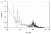
图5为本发明具体实施例的基于频域的改善电源噪声的方法S50中PCB电源网络频域阻抗曲线图;5 is a frequency-domain impedance curve diagram of a PCB power supply network in the method S50 for improving power supply noise based on the frequency domain according to a specific embodiment of the present invention;
图6为本发明具体实施例的基于频域的改善电源噪声的方法S60中电源网络电流噪声频谱分布示意图;6 is a schematic diagram of the spectrum distribution of the current noise of the power supply network in the method S60 of improving power supply noise based on the frequency domain according to a specific embodiment of the present invention;
图7为本发明具体实施例的基于频域的改善电源噪声的方法S70中电压噪声和电流噪声频谱分布峰频点示意图;FIG. 7 is a schematic diagram of peak frequency points of voltage noise and current noise spectrum distribution in frequency domain-based method S70 for improving power supply noise according to a specific embodiment of the present invention;
图8为本发明具体实施例的基于频域的改善电源噪声的方法S110中仿真链路优化前后对比示意图;FIG. 8 is a schematic diagram of a comparison before and after the simulation link optimization in the method S110 for improving power supply noise based on the frequency domain according to a specific embodiment of the present invention;
图9为本发明具体实施例的基于频域的改善电源噪声的方法优化前后电压噪声对比波形图。FIG. 9 is a comparison waveform diagram of voltage noise before and after optimization of the method for improving power supply noise based on the frequency domain according to a specific embodiment of the present invention.
具体实施方式Detailed ways
下面将结合本发明实施例中的附图,对本发明实施例中的技术方案进行清楚、完整地描述,显然,所描述的实施例是本发明一部分实施例,而不是全部的实施例。基于本发明中的实施例,本领域普通技术人员在没有做出创造性劳动前提下所获得的所有其他实施例,都属于本发明保护的范围。The following will clearly and completely describe the technical solutions in the embodiments of the present invention with reference to the accompanying drawings in the embodiments of the present invention. Obviously, the described embodiments are some of the embodiments of the present invention, but not all of them. Based on the embodiments of the present invention, all other embodiments obtained by persons of ordinary skill in the art without making creative efforts belong to the protection scope of the present invention.
实施例1Example 1
参见图1,本发明公开了基于频域的改善电源噪声的方法,包括以下步骤:Referring to Fig. 1, the present invention discloses a method for improving power supply noise based on the frequency domain, comprising the following steps:
S10,确定板极电源网络上电源噪声超标的芯片;S10, determining the chips whose power supply noise exceeds the standard on the board power supply network;
S20,设置示波器的采样率和存储深度;S20, setting the sampling rate and storage depth of the oscilloscope;
S30,保存噪声测试波形为数据格式;S30, saving the noise test waveform as a data format;
S40,对数据格式的波形文件进行离散傅里叶变换,得到电压噪声的频谱分布;S40, performing discrete Fourier transform on the waveform file in the data format to obtain the frequency spectrum distribution of the voltage noise;
S50,利用EDA软件提取PCB电源网络的S参数文件,得到频域阻抗曲线;S50, using EDA software to extract the S parameter file of the PCB power supply network, and obtain the frequency domain impedance curve;
S60,利用频域公式I(f)=(U(f))/(Z(f))计算电源网络的电流噪声频谱分布;S60, using the frequency domain formula I(f)=(U(f))/(Z(f)) to calculate the current noise spectrum distribution of the power supply network;
S70,根据电压噪声频谱分布曲线和电流噪声频谱分布曲线,找到频谱分布的峰频点;S70, according to the voltage noise spectrum distribution curve and the current noise spectrum distribution curve, find the peak frequency point of the spectrum distribution;
S80,根据找到的频谱峰频点,确定对应滤波效果最佳的电容容值;S80, according to the peak frequency point of the frequency spectrum found, determine the capacitance value of the capacitor corresponding to the best filtering effect;
S90,在EDA软件界面下增加或替换最佳的电容容值,并提取相应的板极S参数;S90, add or replace the best capacitance value under the EDA software interface, and extract the corresponding plate S parameters;
S100,将S60获取的电源电流噪声频谱进行逆傅里叶变换,得到时域电流噪声文件;S100, performing an inverse Fourier transform on the power supply current noise spectrum acquired by S60 to obtain a time-domain current noise file;
S110,在EDA软件的ADS中搭建仿真链路,仿真得到增加或替换电容后的时域电压噪声;S110, build a simulation link in the ADS of the EDA software, and simulate the time-domain voltage noise after adding or replacing the capacitor;
S120,通过仿真得到最优改善方案,焊接到PCB上进行实测验证,验证合格后即完成电源噪声的改善。S120, the optimal improvement plan is obtained through simulation, soldered to the PCB for actual measurement and verification, and the improvement of power supply noise is completed after the verification is passed.
上述中,S90目的是在EDA软件中可方便的替换或增减最佳容值电容的数量和位置,并方便的提取S参数,而S参数用于S110中的ADS仿真链路中,如果S110仿真的时域噪声仍然效果不佳,则返回到S90,修改电容数量或位置等信息,重新提取S参数,再导入到S110的仿真链路中仿真,直到时域噪声最佳,为一个循环的过程。有益效果在于,用EDA软件仿真得出结论较快,无需再pcb实物上依次焊接电容来尝试。In the above, the purpose of S90 is to easily replace or increase or decrease the number and position of the capacitor with the best capacitance in the EDA software, and to extract the S parameters conveniently, and the S parameters are used in the ADS simulation link in S110. If S110 If the simulated time-domain noise is still not effective, return to S90, modify the information such as the number or position of capacitors, re-extract the S parameters, and then import them into the simulation link of S110 for simulation until the time-domain noise is optimal, which is a cycle process. The beneficial effect is that it is faster to draw a conclusion by using the EDA software simulation, and there is no need to try welding capacitors on the actual pcb sequentially.
实施例2Example 2
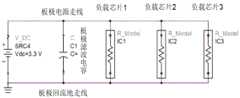
在S10中确定板极电源网络上电源噪声超标的芯片为,用示波器测试每个负载芯片电源和地管脚之间的电源噪声,和芯片手册的要求进行比对,确定超标的芯片,板极电源网络等效电路图参见图2。In S10, it is determined that the chip whose power supply noise exceeds the standard on the board power supply network is, use an oscilloscope to test the power supply noise between the power supply and the ground pin of each load chip, compare it with the requirements of the chip manual, and determine the chip that exceeds the standard, the board See Figure 2 for the equivalent circuit diagram of the power supply network.
S20中,设置示波器的采样率,采样率记为X,数值设置为大于等于电源噪声的最大频率,采样率单位为S/s,即每秒采样一个点;设置示波器的存储深度,存储深度记为L,为示波器保存波形时存储的采样点数量,单位为S,L>=X/Y,其中,Y为电源噪声频谱的最低频率。In S20, set the sampling rate of the oscilloscope, the sampling rate is recorded as X, and the value is set to be greater than or equal to the maximum frequency of power supply noise, and the sampling rate unit is S/s, that is, one point is sampled per second; the storage depth of the oscilloscope is set, and the storage depth is recorded as is L, the number of sampling points stored when the oscilloscope saves the waveform, the unit is S, L>=X/Y, where Y is the lowest frequency of the power supply noise spectrum.
所需的最小的存储深度L与电源噪声频谱最低频率有如下关系,最低频率是10KHz,需满足1/(L/X)≤10KHz,即L≥X/10K=X/10000。The required minimum storage depth L has the following relationship with the lowest frequency of the power supply noise spectrum. The lowest frequency is 10KHz, which must satisfy 1/(L/X)≤10KHz, that is, L≥X/10K=X/10000.
最小采样率与电源噪声的最大频率有关系,如最大频率是20MHz,那采样率至少是20MS/s。The minimum sampling rate is related to the maximum frequency of power supply noise. If the maximum frequency is 20MHz, then the sampling rate should be at least 20MS/s.
一般板极电源噪声频段为10K-20M,因为超出这个频段的噪声,板极滤波电容就无法滤除了,需要靠电源芯片的负反馈电路和芯片封装/DIE上的电容来滤除。Generally, the noise frequency band of the board power supply is 10K-20M. Because the noise beyond this frequency band cannot be filtered by the board filter capacitor, it needs to be filtered by the negative feedback circuit of the power chip and the capacitor on the chip package/DIE.
具体实施例中,板极电源噪声一般分布在10KHz-20MHz,所以示波器采样率至少为X=20MS/s,存储深度至少为:L=X/10K=20M/10K=2000S,其中,MS/s为采样率单位,即Mega Sample per second,每秒采样20兆个点;存储深度2000S代表2000个采样点。In a specific embodiment, the plate power supply noise is generally distributed in 10KHz-20MHz, so the sampling rate of the oscilloscope is at least X=20MS/s, and the storage depth is at least: L=X/10K=20M/10K=2000S, wherein, MS/s It is the sampling rate unit, that is, Mega Sample per second, sampling 20 trillion points per second; the storage depth of 2000S represents 2000 sampling points.
S30中示波器保存的数据格式的波形文件参见图3,第一行为存储深度数据,第二行为采样间隔,即采样率的倒数。Refer to Figure 3 for the waveform file in the data format saved by the oscilloscope in S30. The first line is the storage depth data, and the second line is the sampling interval, which is the reciprocal of the sampling rate.
S40后,得到的电压噪声频谱图参见图4。After S40, see FIG. 4 for the obtained voltage noise spectrum diagram.
S50后,得到的PCB电源网络频域阻抗曲线图参见图5。After S50, see FIG. 5 for the frequency-domain impedance curve of the PCB power network obtained.
S60后,计算出的电源网络电流噪声频谱分布参见图6。After S60, see FIG. 6 for the calculated spectrum distribution of the current noise of the power supply network.
S70中,找到电压噪声和电流噪声频谱分布峰频点参见图7,可见电流噪声谱和电压噪声谱的能量峰在30KHz、60KHz、95KHz、140KHz和1MHz,对应30KHz-140KHz噪声最佳滤波电容容值是220uF,1MHz噪声最佳滤波电容容值是10uF。In the S70, find the peak frequency points of the voltage noise and current noise spectrum distribution. See Figure 7. It can be seen that the energy peaks of the current noise spectrum and voltage noise spectrum are at 30KHz, 60KHz, 95KHz, 140KHz and 1MHz, corresponding to the best filter capacitance for 30KHz-140KHz noise. The value is 220uF, and the best filter capacitor value for 1MHz noise is 10uF.
S110中仿真链路优化前后对比示意图参见图8,上半部分为优化前、下半部分为优化后。Refer to Figure 8 for a comparison diagram of the simulation link before and after optimization in S110, the upper half is before optimization, and the lower half is after optimization.
优化前后电压噪声对比波形图参见图9,10为优化前的电压,即图8中的V_PATENT;20为优化后的电压,即图8中的V_PATENT_OPI。可以看到,优化后的电压噪声峰峰值显著降低。Refer to Figure 9 for the comparison waveform of voltage noise before and after optimization, 10 is the voltage before optimization, that is, V_PATENT in Figure 8; 20 is the voltage after optimization, that is, V_PATENT_OPI in Figure 8. It can be seen that the peak-to-peak voltage noise is significantly reduced after optimization.
具体实施例中,EDA软件包括POWERSI或OPI。In a specific embodiment, the EDA software includes POWERSI or OPI.
应当理解,本文所述的示例性实施例是说明性的而非限制性的。尽管结合附图描述了本发明的一个或多个实施例,本领域普通技术人员应当理解,在不脱离通过所附权利要求所限定的本发明的精神和范围的情况下,可以做出各种形式和细节的改变。It should be understood that the exemplary embodiments described herein are illustrative and not restrictive. Although one or more embodiments of the present invention have been described in conjunction with the drawings, it will be appreciated by those of ordinary skill in the art that various changes may be made without departing from the spirit and scope of the invention as defined by the appended claims. Changes in form and detail.
Claims (6)
Translated fromChinesePriority Applications (1)
| Application Number | Priority Date | Filing Date | Title |
|---|---|---|---|
| CN201910984138.2ACN110781642B (en) | 2019-10-16 | 2019-10-16 | Method for improving power supply noise based on frequency domain |
Applications Claiming Priority (1)
| Application Number | Priority Date | Filing Date | Title |
|---|---|---|---|
| CN201910984138.2ACN110781642B (en) | 2019-10-16 | 2019-10-16 | Method for improving power supply noise based on frequency domain |
Publications (2)
| Publication Number | Publication Date |
|---|---|
| CN110781642A CN110781642A (en) | 2020-02-11 |
| CN110781642Btrue CN110781642B (en) | 2023-05-19 |
Family
ID=69385748
Family Applications (1)
| Application Number | Title | Priority Date | Filing Date |
|---|---|---|---|
| CN201910984138.2AActiveCN110781642B (en) | 2019-10-16 | 2019-10-16 | Method for improving power supply noise based on frequency domain |
Country Status (1)
| Country | Link |
|---|---|
| CN (1) | CN110781642B (en) |
Families Citing this family (1)
| Publication number | Priority date | Publication date | Assignee | Title |
|---|---|---|---|---|
| US12320830B2 (en) | 2022-04-22 | 2025-06-03 | Changxin Memory Technologies, Inc. | Method, device and system for measuring frequency domain characteristics, and storage medium |
Citations (3)
| Publication number | Priority date | Publication date | Assignee | Title |
|---|---|---|---|---|
| CN101872377A (en)* | 2010-06-12 | 2010-10-27 | 清华大学 | A Method of Using Decoupling Capacitors to Suppress Noise in Integrated Circuit Power Supply Network |
| CN105956289A (en)* | 2016-05-06 | 2016-09-21 | 西安电子科技大学 | Power distribution network design method based on decoupling region of decoupling capacitor |
| CN108616127A (en)* | 2016-12-12 | 2018-10-02 | 中国航空工业集团公司西安航空计算技术研究所 | A kind of automatic filter capacitor design method that time-frequency domain combines |
Family Cites Families (3)
| Publication number | Priority date | Publication date | Assignee | Title |
|---|---|---|---|---|
| JP5035039B2 (en)* | 2008-03-11 | 2012-09-26 | 日本電気株式会社 | Electronic circuit board power noise analysis method, system and program |
| US8521500B2 (en)* | 2010-08-24 | 2013-08-27 | International Business Machines Corporation | Method and device for measuring integrated circuit power supply noise and calibration of power supply noise analysis models |
| US10324122B2 (en)* | 2015-12-14 | 2019-06-18 | International Business Machines Corporation | Predicting noise propagation in circuits |
- 2019
- 2019-10-16CNCN201910984138.2Apatent/CN110781642B/enactiveActive
Patent Citations (3)
| Publication number | Priority date | Publication date | Assignee | Title |
|---|---|---|---|---|
| CN101872377A (en)* | 2010-06-12 | 2010-10-27 | 清华大学 | A Method of Using Decoupling Capacitors to Suppress Noise in Integrated Circuit Power Supply Network |
| CN105956289A (en)* | 2016-05-06 | 2016-09-21 | 西安电子科技大学 | Power distribution network design method based on decoupling region of decoupling capacitor |
| CN108616127A (en)* | 2016-12-12 | 2018-10-02 | 中国航空工业集团公司西安航空计算技术研究所 | A kind of automatic filter capacitor design method that time-frequency domain combines |
Non-Patent Citations (3)
| Title |
|---|
| Lhsan Erdin.Delta4 Noise Suppression Techniques in Printed Circuit Boards for Clock Frequencies Over 50 Mhz.《Restrictions apply》.2003,1132-1135.* |
| 刘洋 ; 白钰杰 ; 罗厚兴 ; 夏建强 ; .基于最大时域瞬态噪声的去耦电容选择方法.电子与信息学报.2017,(第11期),2763-2769.* |
| 胡晋,等.基于改进时频域混合方法的系统级电源完整性仿真.《第十九届计算机工程与工艺年会暨第五届微处理器技术论坛论文集》.2015,451-455.* |
Also Published As
| Publication number | Publication date |
|---|---|
| CN110781642A (en) | 2020-02-11 |
Similar Documents
| Publication | Publication Date | Title |
|---|---|---|
| CN112528580A (en) | Electromagnetic radiation simulation prediction method for flyback converter circuit board | |
| CN110781642B (en) | Method for improving power supply noise based on frequency domain | |
| CN107167724A (en) | What a kind of small-signal was measured goes embedding method | |
| KR20210009771A (en) | System and method for diagnosing partial discharge of electric power equipment, and a recording medium having computer readable program for executing the method | |
| CN118473191B (en) | Flyback chip monitoring and evaluating method, system and equipment based on FPGA | |
| CN101149762A (en) | High frequency equivalent circuit structure for on-chip inductor and its parameter calculation method | |
| CN110348039A (en) | A kind of decoupling capacitor design method for printed circuit board | |
| CN117391019B (en) | Simulation test method, device, equipment and medium for EMI power filter | |
| JP2008096391A (en) | Conduction noise simulator, conduction noise simulation method, and conduction noise simulation program | |
| KR102028921B1 (en) | Device for measuring integrated circuit current and method for measuring integrated circuit current using the device | |
| CN100401306C (en) | Modeling device and method for a capacitance equivalent model | |
| CN116973798A (en) | Frequency domain characteristic measuring method, device, system and storage medium | |
| CN114545120A (en) | Method, device, equipment and medium for testing radiation interference resistance of server | |
| CN118209797A (en) | Method and system for testing electronic element | |
| CN108616127B (en) | Time-frequency domain combined automatic filter capacitor design method | |
| CN109740272A (en) | A kind of inspection method and related device for inductive compensation in PCB | |
| CN107917661A (en) | Function inspection device for frequency-responsive winding deformation tester | |
| Clarke et al. | Characterising non-linear behaviour of coupling capacitors through audio feature analysis and machine learning | |
| CN114757143A (en) | Decoupling capacitor selection method and device, server and readable storage medium | |
| CN114414631A (en) | Nondestructive evaluation method of welding layer sintering quality based on time-frequency domain analysis of electrical pulse signal | |
| CN116227424A (en) | Low dropout linear voltage regulator noise suppression universal board, design and test method | |
| CN118228681B (en) | Method and system for optimizing impedance of power distribution network of digital system | |
| CN113468837A (en) | Method and system for estimating salient fast current of chip power supply network | |
| CN119598175B (en) | Feature extraction method and system for self-healing voltage information of metallized film capacitors | |
| CN111310879A (en) | Testing device and method for online adjustment of antenna parameters of RFID system |
Legal Events
| Date | Code | Title | Description |
|---|---|---|---|
| PB01 | Publication | ||
| PB01 | Publication | ||
| SE01 | Entry into force of request for substantive examination | ||
| SE01 | Entry into force of request for substantive examination | ||
| GR01 | Patent grant | ||
| GR01 | Patent grant |