CN110779931A - Semiconductor defect detection equipment - Google Patents
Semiconductor defect detection equipmentDownload PDFInfo
- Publication number
- CN110779931A CN110779931ACN201910650170.7ACN201910650170ACN110779931ACN 110779931 ACN110779931 ACN 110779931ACN 201910650170 ACN201910650170 ACN 201910650170ACN 110779931 ACN110779931 ACN 110779931A
- Authority
- CN
- China
- Prior art keywords
- image
- optical system
- semiconductor defect
- semiconductor
- infrared
- Prior art date
- Legal status (The legal status is an assumption and is not a legal conclusion. Google has not performed a legal analysis and makes no representation as to the accuracy of the status listed.)
- Pending
Links
- 239000004065semiconductorSubstances0.000titleclaimsabstractdescription52
- 230000007547defectEffects0.000titleclaimsabstractdescription50
- 238000001514detection methodMethods0.000titleclaimsabstractdescription34
- 230000003287optical effectEffects0.000claimsabstractdescription49
- 238000005286illuminationMethods0.000claimsabstractdescription32
- 238000012545processingMethods0.000claimsabstractdescription16
- 230000005540biological transmissionEffects0.000claimsabstractdescription7
- 238000007689inspectionMethods0.000claimsdescription31
- 230000010287polarizationEffects0.000claimsdescription13
- 230000007246mechanismEffects0.000claimsdescription9
- 229910052736halogenInorganic materials0.000claimsdescription3
- 150000002367halogensChemical class0.000claimsdescription3
- 238000012360testing methodMethods0.000claimsdescription3
- 239000000758substrateSubstances0.000claimsdescription2
- 230000000694effectsEffects0.000description11
- 238000000034methodMethods0.000description9
- 238000010586diagramMethods0.000description6
- 235000012431wafersNutrition0.000description5
- 238000004519manufacturing processMethods0.000description4
- 238000010521absorption reactionMethods0.000description3
- XUIMIQQOPSSXEZ-UHFFFAOYSA-NSiliconChemical compound[Si]XUIMIQQOPSSXEZ-UHFFFAOYSA-N0.000description2
- 230000008569processEffects0.000description2
- 229910052710siliconInorganic materials0.000description2
- 239000010703siliconSubstances0.000description2
- 238000004458analytical methodMethods0.000description1
- 238000006243chemical reactionMethods0.000description1
- 238000013461designMethods0.000description1
- 238000011161developmentMethods0.000description1
- 238000005516engineering processMethods0.000description1
- 230000031700light absorptionEffects0.000description1
- 239000000463materialSubstances0.000description1
- 230000005499meniscusEffects0.000description1
- 238000012986modificationMethods0.000description1
- 230000004048modificationEffects0.000description1
- 230000009467reductionEffects0.000description1
Images


Classifications
- G—PHYSICS
- G01—MEASURING; TESTING
- G01N—INVESTIGATING OR ANALYSING MATERIALS BY DETERMINING THEIR CHEMICAL OR PHYSICAL PROPERTIES
- G01N21/00—Investigating or analysing materials by the use of optical means, i.e. using sub-millimetre waves, infrared, visible or ultraviolet light
- G01N21/84—Systems specially adapted for particular applications
- G01N21/88—Investigating the presence of flaws or contamination
- G01N21/95—Investigating the presence of flaws or contamination characterised by the material or shape of the object to be examined
- G01N21/9501—Semiconductor wafers
- G01N21/9505—Wafer internal defects, e.g. microcracks
- G—PHYSICS
- G02—OPTICS
- G02B—OPTICAL ELEMENTS, SYSTEMS OR APPARATUS
- G02B21/00—Microscopes
- G02B21/06—Means for illuminating specimens
- G—PHYSICS
- G02—OPTICS
- G02B—OPTICAL ELEMENTS, SYSTEMS OR APPARATUS
- G02B21/00—Microscopes
- G02B21/36—Microscopes arranged for photographic purposes or projection purposes or digital imaging or video purposes including associated control and data processing arrangements
- G02B21/365—Control or image processing arrangements for digital or video microscopes
- H—ELECTRICITY
- H04—ELECTRIC COMMUNICATION TECHNIQUE
- H04N—PICTORIAL COMMUNICATION, e.g. TELEVISION
- H04N23/00—Cameras or camera modules comprising electronic image sensors; Control thereof
- H04N23/20—Cameras or camera modules comprising electronic image sensors; Control thereof for generating image signals from infrared radiation only
- H04N23/21—Cameras or camera modules comprising electronic image sensors; Control thereof for generating image signals from infrared radiation only from near infrared [NIR] radiation
- H—ELECTRICITY
- H04—ELECTRIC COMMUNICATION TECHNIQUE
- H04N—PICTORIAL COMMUNICATION, e.g. TELEVISION
- H04N23/00—Cameras or camera modules comprising electronic image sensors; Control thereof
- H04N23/50—Constructional details
- H04N23/55—Optical parts specially adapted for electronic image sensors; Mounting thereof
- H—ELECTRICITY
- H04—ELECTRIC COMMUNICATION TECHNIQUE
- H04N—PICTORIAL COMMUNICATION, e.g. TELEVISION
- H04N23/00—Cameras or camera modules comprising electronic image sensors; Control thereof
- H04N23/56—Cameras or camera modules comprising electronic image sensors; Control thereof provided with illuminating means
- G—PHYSICS
- G02—OPTICS
- G02B—OPTICAL ELEMENTS, SYSTEMS OR APPARATUS
- G02B27/00—Optical systems or apparatus not provided for by any of the groups G02B1/00 - G02B26/00, G02B30/00
- G02B27/48—Laser speckle optics
- H—ELECTRICITY
- H01—ELECTRIC ELEMENTS
- H01L—SEMICONDUCTOR DEVICES NOT COVERED BY CLASS H10
- H01L21/00—Processes or apparatus adapted for the manufacture or treatment of semiconductor or solid state devices or of parts thereof
- H01L21/67—Apparatus specially adapted for handling semiconductor or electric solid state devices during manufacture or treatment thereof; Apparatus specially adapted for handling wafers during manufacture or treatment of semiconductor or electric solid state devices or components ; Apparatus not specifically provided for elsewhere
- H01L21/67005—Apparatus not specifically provided for elsewhere
- H01L21/67242—Apparatus for monitoring, sorting or marking
- H01L21/67288—Monitoring of warpage, curvature, damage, defects or the like
Landscapes
- Engineering & Computer Science (AREA)
- Physics & Mathematics (AREA)
- Multimedia (AREA)
- General Physics & Mathematics (AREA)
- Health & Medical Sciences (AREA)
- Chemical & Material Sciences (AREA)
- Analytical Chemistry (AREA)
- Signal Processing (AREA)
- Biochemistry (AREA)
- Pathology (AREA)
- Immunology (AREA)
- Toxicology (AREA)
- General Health & Medical Sciences (AREA)
- Life Sciences & Earth Sciences (AREA)
- Optics & Photonics (AREA)
- Manufacturing & Machinery (AREA)
- Computer Hardware Design (AREA)
- Microelectronics & Electronic Packaging (AREA)
- Power Engineering (AREA)
- Condensed Matter Physics & Semiconductors (AREA)
- Computer Vision & Pattern Recognition (AREA)
- Investigating Materials By The Use Of Optical Means Adapted For Particular Applications (AREA)
- Testing Or Measuring Of Semiconductors Or The Like (AREA)
Abstract
Description
Translated fromChinese技术领域technical field
本发明涉及一种检测设备,尤其涉及一种半导体瑕疵检测设备。The present invention relates to a detection device, in particular to a semiconductor defect detection device.
背景技术Background technique
随着科技发展,人们对于电子产品中电子构件的精密程度及品质需求越 来越高。举例来说,电子产品中电路板上的各种元件的品质及外观检测为制 造及检验过程中的重要步骤,以确保电路板的功能正常。在目前,硅晶圆内 层的检测常以面型扫描相机最为常见。然而,如何设计或改良现有检测设备 及技术方法,以增加扫描速度,进一步优化检测流程以提升硅晶圆的产能, 是本领域技术人员共同致力于研究的。With the development of science and technology, people have higher and higher requirements for the precision and quality of electronic components in electronic products. For example, quality and appearance inspection of various components on circuit boards in electronic products is an important step in the manufacturing and inspection process to ensure that the circuit boards function properly. At present, the inspection of the inner layers of silicon wafers is often the most common with area scanning cameras. However, how to design or improve the existing inspection equipment and technical methods to increase the scanning speed and further optimize the inspection process to increase the productivity of silicon wafers is a joint effort of those skilled in the art.
发明内容SUMMARY OF THE INVENTION
本发明提供一种半导体瑕疵检测设备,可提升半导体瑕疵检测设备的光 学品质及检测效果。The present invention provides a semiconductor defect detection device, which can improve the optical quality and detection effect of the semiconductor defect detection device.
本发明提供一种半导体瑕疵检测设备,用于检测待测物的气泡瑕疵,包 含载台、光学系统、红外线图像获取装置以及处理单元。载台适于承载待测 物。光学系统提供照明光束至待测物以产生图像光束。红外线图像获取装置 配置于图像光束的传递路径上。红外线图像获取装置适于接收图像光束以转 换为图像信息。处理单元电性连接红外线图像获取装置,适于依据图像信息 对待测物进行分析。The present invention provides a semiconductor defect detection device, which is used to detect the bubble defect of the object to be tested, and comprises a stage, an optical system, an infrared image acquisition device and a processing unit. The stage is suitable for carrying the object to be tested. The optical system provides an illumination beam to the object to be tested to generate an image beam. The infrared image acquisition device is arranged on the transmission path of the image beam. The infrared image acquisition device is adapted to receive the image beam for conversion into image information. The processing unit is electrically connected to the infrared image acquisition device, and is suitable for analyzing the object to be measured according to the image information.
基于上述,本发明的半导体瑕疵检测设备可提升半导体瑕疵检测设备的 检测效果及有效提高产品的产能。Based on the above, the semiconductor defect detection device of the present invention can improve the detection effect of the semiconductor defect detection device and effectively improve the productivity of products.
为让本发明的上述特征和优点能更明显易懂,下文特举实施例,并配合 附图作详细说明如下。In order to make the above-mentioned features and advantages of the present invention more obvious and easy to understand, the following embodiments are given and described in detail with the accompanying drawings as follows.
附图说明Description of drawings
图1为本发明一实施例的半导体瑕疵检测设备的示意图;FIG. 1 is a schematic diagram of a semiconductor defect detection apparatus according to an embodiment of the present invention;
图2为本发明另一实施例的半导体瑕疵检测设备的示意图;2 is a schematic diagram of a semiconductor defect detection apparatus according to another embodiment of the present invention;
图3为本发明另一实施例的半导体瑕疵检测设备的示意图;3 is a schematic diagram of a semiconductor defect detection apparatus according to another embodiment of the present invention;
图4为本发明一实施例的半导体晶圆缺陷的检测方法。FIG. 4 is a method for detecting semiconductor wafer defects according to an embodiment of the present invention.
附图标号说明:Description of reference numbers:
10:待测物10: Object to be tested
20:输送设备20: Conveying equipment
100、100A、100B:电子装置100, 100A, 100B: Electronic devices
110:载台110: Stage
120、120A:光学系统120, 120A: Optical system
122:光源122: light source
124:分光元件124: Spectroscopic element
126:偏振元件126: Polarizing element
128:调整机构128: Adjustment Mechanism
130:红外线图像获取装置130: Infrared image acquisition device
132:感光元件132: Photosensitive element
140:处理单元140: Processing unit
LB:照明光束LB: Lighting beam
LI:图像光束LI: Image beam
S300、S310、S320:步骤S300, S310, S320: Steps
具体实施方式Detailed ways
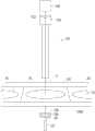
图1为本发明一实施例的半导体瑕疵检测设备的示意图。请参考图1, 在本实施例中,半导体瑕疵检测设备100包含载台110、光学系统120、红外 线图像获取装置130以及处理单元140。载台110适于承载待测物10。在本 实施例中,待测物10,包含但不限于,可为半导体基板、半导体晶圆或半导 体封装芯片等类似半导体物件。具体而言,本实施例的半导体瑕疵检测设备 100的检测项目,包含但不限于,适用于检测待测物10内层的气泡瑕疵,从而可改善待测物10的制作手段以提升产能,但本发明并不限于此。FIG. 1 is a schematic diagram of a semiconductor defect inspection apparatus according to an embodiment of the present invention. Referring to FIG. 1 , in this embodiment, the semiconductor defect inspection apparatus 100 includes a
光学系统120适于提供照明光束LB至待测物10,并产生图像光束LI以 及接收并传递图像光束LI至红外线图像获取装置130进行后续的运算处理。 光学系统120包含光源122。具体而言,光学系统120例如是具有聚焦透镜、 反射镜或其他光学元件等构件组合的光学镜头或光学装置。在一些实施例中, 照明光束LB为可见光,但在一些实施例中,照明光束LB可以是近红外光或 短波长红外光,本发明并不限于此。The
光源122适于提供照明光束LB至待测物10以产生图像光束LI。详细而 言,在本实施例中,光源122为卤素灯。然而,在后续说明的其他实施例中, 照明光束LB可为红外激光,本发明并不限于此。The
红外线图像获取装置130配置于图像光束LI的传递路径上,适于接收图 像光束LI,将图像光束LI的光学图像转换为电子信号。具体而言,红外线图 像获取装置130包含感光元件132,适于接收图像光束LI以转换为图像信息。 感光元件132例如是电荷耦合器件(Charge-coupled Device,CCD)。在本实 施例中,红外线图像获取装置130为面型扫描相机,因此可控制载台110的 移动而对待测物10进行面拍摄。在一些实施例中,红外线图像获取装置130 可视需求配置具有屈光度的一或多个光学镜片的组合,例如包含双凹透镜、 双凸透镜、凹凸透镜、凸凹透镜、平凸透镜以及平凹透镜等非平面镜片的各 种组合,以协助引导图像光束LI,但本发明并不限于此。在本实施例中,待 测物10对照明光束LB中各波长的吸收程度以可见光及红外光为主,且在波 长约400纳米至900纳米具有良好的吸光强度。The infrared
请继续参考图1。处理单元140电性连接红外线图像获取装置130,适于 依据所接收到的电子信号进行分析。具体而言,处理单元140与感光元件132 电线连接,并依据上述的图像信息对待测物10进行分析。处理单元140例如 为中央处理单元(CentralProcessing Unit,CPU),或是其他可程序化的一般 用途或特殊用途的微处理器(Microprocessor)、数字信号处理器(Digital Signal Processor,DSP)、可程序化控制器、特殊应用集成电路(Application Specific Integrated Circuit,ASIC)或其他类似元件或上述元件的组合,本发明并不限 于此。Please continue to refer to Figure 1. The
在本实施例中,光学系统120还包含偏振元件126,配置于光源122与 载台110之间。偏振元件126例如为线偏振片,使得光源122所发出的照明 光束LB传递通过偏振元件126而产生线偏振状态的照明光束LB。在一些实 施例中,偏振元件126还可以例如是圆偏振片或椭圆偏振片,本发明并不限 于此。因此,将使得红外线图像获取装置130可获取到待测物10的对应不同 深度位置的光学图像。换句话说,不同方向的线偏振状态的照明光束LB在待测物10上的照射深度位置不同。因此,可通过调整偏振元件126的偏振角 度而使红外线图像获取装置130获得不同深度位置的光学图像。如此一来, 可依据待测物10的材料与特性或者是不同的需求程度进一步配置并调整偏 振元件126以提升光学图像的显示效果。In this embodiment, the
在本实施例中,光学系统120还包含调整机构128,配置于光源122与 载台110之间,适于调整偏振元件126的偏振角度。举例而言,调整机构128 例如是一个可控制偏振元件126的自动化机构,可依据所给予的特定电路信 号旋转特定角度,进一步带动偏振元件126旋转以调整照明光束LB的偏振 状态。举例而言,调整机构128可事先经过设定,而进一步控制偏振元件126 例如旋转5度,并使红外线图像获取装置130自动取像。然而,在其他实施 例中,调整机构128也可以为手动旋转方式进行调整,本发明并不限制调整 机构128的种类及调整进行方式。In this embodiment, the
换句话说,本实施例的光学系统120为透射式光学系统。然而在其他实 施例中,图1的实施例还可以依需求而采用反射式光学系统(如图4的光学 系统120A),但本发明并不限于此。In other words, the
图2为本发明另一实施例的半导体瑕疵检测设备的示意图。请参考图2。 本实施例的半导体瑕疵检测设备100A类似于图1的半导体瑕疵检测设备100, 惟两者不同之处在于,在本实施例中,半导体瑕疵检测设备100A的光源122 为可提供激光的发光装置,例如是使用低散斑激光装置(Speckle Reduction Laser)。因此,照明光束LB为激光。而在本实施例中,照明光束LB例如 是中心波长大致为1250纳米至1350纳米的红外光。FIG. 2 is a schematic diagram of a semiconductor defect inspection apparatus according to another embodiment of the present invention. Please refer to Figure 2. The semiconductor
除此之外,由于激光的功率密度高,可达一般发光二极管的功率密度的 数倍到数百倍,故本实施例的红外线图像获取装置130可使用高速线型扫描 相机,因此可通过额外的输送设备20输送载台110而对待测物10进行线拍 摄。如此一来,可提高发光功率密度以提升半导体瑕疵检测设备100A的光 学品质及检测效果,并降低光学系统120的成本。在本实施例中,待测物10 对于波长大致为1300纳米的照明光束LB的吸收程度较高且能使图像清晰, 因此可以展现较佳的检测效能,进而提升光学检测设备100A的光学品质及 检测效果。In addition, since the power density of the laser is high, which can be several times to hundreds of times that of a general light-emitting diode, the infrared
图3为本发明另一实施例的半导体瑕疵检测设备的示意图。请参考图3。 本实施例的半导体瑕疵检测设备100B类似于图2的半导体瑕疵检测设备 100A,两者不同之处在于,在本实施例中,半导体瑕疵检测设备100B的光 学系统120A为反射式光学系统。具体而言,光学系统120还包含分光元件 124,配置于照明光束LB及图像光束LI的传递路径上,例如是分光镜,适 于反射照明光束LB以及让图像光束LI通过。此外,在一些实施例中,光学 系统120A还可选择性地包含反射元件,用于将光源122发出的照明光束LB 引导至待测物10。然而,本发明不限于此,于其它实施例中,也可利用其它 种类光学元件将照明光束LB引导至待测物10。此外,检测设备半导体瑕疵 检测设备100B的光源122为可提供波长中心波长大致为1500纳米至1600 纳米激光的发光装置。如此一来,可提高发光功率密度以提升半导体瑕疵检 测设备100的光学品质及检测效果,并降低光学系统120A的成本。在本实 施例中,待测物10对于波长大致为1550纳米的照明光束LB的吸收程度较 高且能使图像清晰,因此可以展现较佳的检测效能,进而提升光学检测设备 100B的光学品质及检测效果。FIG. 3 is a schematic diagram of a semiconductor defect inspection apparatus according to another embodiment of the present invention. Please refer to Figure 3. The semiconductor
图4为本发明一实施例的半导体晶圆缺陷的检测方法。请参考图3及图 4。本实施例的检测方法至少可应用于图3所显示的半导体瑕疵检测设备100B, 故以下说明将以图3的半导体瑕疵检测设备100B为例,但本发明并不限于此。 在本实施例的检测方法中,首先,执行步骤S300,提供照明光束LB至待测 物10以产生图像光束LI。具体而言,可由半导体瑕疵检测设备100B的光源 122提供照明光束LB,以使待测物10经照射而反射出可反应显示待测物10 结构的图像光束LI。FIG. 4 is a method for detecting semiconductor wafer defects according to an embodiment of the present invention. Please refer to Figure 3 and Figure 4. The inspection method of this embodiment can be applied to at least the semiconductor
接着,在上述步骤S300之后,执行步骤S310,接收图像光束LI1以转 换为图像信息。具体而言,可由半导体瑕疵检测设备100B的红外线图像获取 装置130接收图像光束LI1,进而产生图像信息并提供至处理单元140进行识 别或检测。接着,在上述步骤S310之后,执行步骤S320,依据图像信息对 待测物10进行分析。具体而言,可通过处理单元140的中数据的图像比对及 运算处理对待测物10进行分析以产生出一个检测结果。如此一来,可提升半 导体瑕疵检测设备100B的光学品质及检测效果,从而可改善待测物10的制 作手段以提升产能。Next, after the above step S300, step S310 is executed to receive the image light beam LI1 to convert it into image information. Specifically, the image light beam LI1 can be received by the infrared
在其他的实施例中,上述提供照明光束LB至待测物10以产生图像光束 LI的方法还包含提供照明光束LB至偏振元件126的步骤,以及调整偏振元 件126的偏振角度以调整照明光束LB的偏振状态。如此一来,可进一步依 据照明光束LB不同的偏振状态或偏振方向而获得不同的光学图像,进而提 升半导体瑕疵检测设备100B的光学图像显示效果及对待测物10的检测效果。In other embodiments, the above-mentioned method for providing the illumination beam LB to the object under
综上所述,本发明的半导体瑕疵检测设备可提升半导体瑕疵检测设备的 光学品质及检测效果,从而可改善待测物的制作手段以提升产能。To sum up, the semiconductor defect detection device of the present invention can improve the optical quality and detection effect of the semiconductor defect detection device, thereby improving the manufacturing method of the object to be tested and increasing the productivity.
虽然本发明已以实施例揭示如上,然其并非用以限定本发明,任何所属 技术领域中技术人员,在不脱离本发明的精神和范围内,当可作些许的更改 与润饰,故本发明的保护范围当视权利要求所界定的为准。Although the present invention has been disclosed above with examples, it is not intended to limit the present invention. Any person skilled in the art can make some changes and modifications without departing from the spirit and scope of the present invention. Therefore, the present invention The scope of protection shall be subject to what is defined in the claims.
Claims (13)
Applications Claiming Priority (2)
| Application Number | Priority Date | Filing Date | Title |
|---|---|---|---|
| TW107126453 | 2018-07-31 | ||
| TW107126453ATWI705244B (en) | 2018-07-31 | 2018-07-31 | Semiconductor defects inspection apparatus |
Publications (1)
| Publication Number | Publication Date |
|---|---|
| CN110779931Atrue CN110779931A (en) | 2020-02-11 |
Family
ID=69228969
Family Applications (1)
| Application Number | Title | Priority Date | Filing Date |
|---|---|---|---|
| CN201910650170.7APendingCN110779931A (en) | 2018-07-31 | 2019-07-18 | Semiconductor defect detection equipment |
Country Status (3)
| Country | Link |
|---|---|
| US (1) | US10763148B2 (en) |
| CN (1) | CN110779931A (en) |
| TW (1) | TWI705244B (en) |
Cited By (1)
| Publication number | Priority date | Publication date | Assignee | Title |
|---|---|---|---|---|
| CN113658882A (en)* | 2021-08-18 | 2021-11-16 | 颜鸿任 | Imaging method for bubble defects in semiconductor packaging sealing adhesive based on optical interference fault |
Families Citing this family (3)
| Publication number | Priority date | Publication date | Assignee | Title |
|---|---|---|---|---|
| TWI803132B (en)* | 2022-01-04 | 2023-05-21 | 逢甲大學 | Automatic double-sided optical inspection device |
| TWI832136B (en)* | 2022-01-10 | 2024-02-11 | 致茂電子股份有限公司 | Inspection system for semiconductor device with metal coating |
| TWI878968B (en)* | 2023-07-10 | 2025-04-01 | 奇景光電股份有限公司 | Optical measurement system |
Citations (13)
| Publication number | Priority date | Publication date | Assignee | Title |
|---|---|---|---|---|
| US20040179193A1 (en)* | 2001-07-05 | 2004-09-16 | Shinji Maezono | Method and device for inspecting defect of sheet-shaped transparent body |
| CN101151513A (en)* | 2005-02-09 | 2008-03-26 | 音莱特解决方案有限公司 | Methods and apparatus for noninvasive determinations of analytes |
| US20100165095A1 (en)* | 2008-06-27 | 2010-07-01 | Nippon Electro-Sensory Devices Corporation | Defect inspection device and defect inspection method for silicon wafer |
| US20110090507A1 (en)* | 2009-09-14 | 2011-04-21 | Lg Chem. Ltd. | Apparatus for detecting foreign material in pouch type battery |
| US20120044279A1 (en)* | 2009-04-27 | 2012-02-23 | Hiroshi Uchino | Image Projection Apparatus and Laser Beam Projection Apparatus |
| US8169613B1 (en)* | 2008-11-21 | 2012-05-01 | Kla-Tencor Corp. | Segmented polarizer for optimizing performance of a surface inspection system |
| US20130162980A1 (en)* | 2011-12-22 | 2013-06-27 | Samsung Electro-Mechanics Co., Ltd. | Apparatus for non-invasively inspecting defects and method for inspecting defects using the same |
| CN103445764A (en)* | 2013-09-04 | 2013-12-18 | 广州医软智能科技有限公司 | Device and method for monitoring microcirculation imaging |
| US20140233024A1 (en)* | 2011-07-29 | 2014-08-21 | Hitachi High-Techmologies Corporation | Defect Inspecting Apparatus and Defect Inspecting Method |
| CN105911072A (en)* | 2016-06-08 | 2016-08-31 | 浙江工业大学 | Optical rapid detection device for minor flaws on surfaces of spheres |
| US9553034B1 (en)* | 2012-03-27 | 2017-01-24 | Kla-Tencor Corporation | Combined semiconductor metrology system |
| CN106442538A (en)* | 2016-08-22 | 2017-02-22 | 中国电子科技集团公司第四十研究所 | Optical element damage detecting device and method based on polarization imaging |
| CN206618705U (en)* | 2017-02-24 | 2017-11-07 | 湖南远见视觉科技有限责任公司 | A kind of optical film defect detecting device |
Family Cites Families (7)
| Publication number | Priority date | Publication date | Assignee | Title |
|---|---|---|---|---|
| JP5187843B2 (en)* | 2008-09-01 | 2013-04-24 | 浜松ホトニクス株式会社 | Semiconductor inspection apparatus and inspection method |
| TWI394946B (en)* | 2008-09-02 | 2013-05-01 | Univ Nat Formosa | Method and device for measuring object defect |
| KR101214806B1 (en)* | 2010-05-11 | 2012-12-24 | 가부시키가이샤 사무코 | Apparatus and method for defect inspection of wafer |
| CN102590221A (en)* | 2012-02-24 | 2012-07-18 | 深圳大学 | Apparent defect detecting system and detecting method of polarizer |
| WO2015174388A1 (en)* | 2014-05-15 | 2015-11-19 | 株式会社オキサイド | Deep ultraviolet laser generation device and light source device |
| KR20160115682A (en)* | 2015-03-25 | 2016-10-06 | 삼성전자주식회사 | Method of enabling spatially varying auto focusing of objects and an image capturing system thereof |
| JP6752638B2 (en)* | 2016-06-27 | 2020-09-09 | 株式会社ディスコ | Internal crack detection method and internal crack detection device |
- 2018
- 2018-07-31TWTW107126453Apatent/TWI705244B/enactive
- 2019
- 2019-05-23USUS16/420,188patent/US10763148B2/enactiveActive
- 2019-07-18CNCN201910650170.7Apatent/CN110779931A/enactivePending
Patent Citations (13)
| Publication number | Priority date | Publication date | Assignee | Title |
|---|---|---|---|---|
| US20040179193A1 (en)* | 2001-07-05 | 2004-09-16 | Shinji Maezono | Method and device for inspecting defect of sheet-shaped transparent body |
| CN101151513A (en)* | 2005-02-09 | 2008-03-26 | 音莱特解决方案有限公司 | Methods and apparatus for noninvasive determinations of analytes |
| US20100165095A1 (en)* | 2008-06-27 | 2010-07-01 | Nippon Electro-Sensory Devices Corporation | Defect inspection device and defect inspection method for silicon wafer |
| US8169613B1 (en)* | 2008-11-21 | 2012-05-01 | Kla-Tencor Corp. | Segmented polarizer for optimizing performance of a surface inspection system |
| US20120044279A1 (en)* | 2009-04-27 | 2012-02-23 | Hiroshi Uchino | Image Projection Apparatus and Laser Beam Projection Apparatus |
| US20110090507A1 (en)* | 2009-09-14 | 2011-04-21 | Lg Chem. Ltd. | Apparatus for detecting foreign material in pouch type battery |
| US20140233024A1 (en)* | 2011-07-29 | 2014-08-21 | Hitachi High-Techmologies Corporation | Defect Inspecting Apparatus and Defect Inspecting Method |
| US20130162980A1 (en)* | 2011-12-22 | 2013-06-27 | Samsung Electro-Mechanics Co., Ltd. | Apparatus for non-invasively inspecting defects and method for inspecting defects using the same |
| US9553034B1 (en)* | 2012-03-27 | 2017-01-24 | Kla-Tencor Corporation | Combined semiconductor metrology system |
| CN103445764A (en)* | 2013-09-04 | 2013-12-18 | 广州医软智能科技有限公司 | Device and method for monitoring microcirculation imaging |
| CN105911072A (en)* | 2016-06-08 | 2016-08-31 | 浙江工业大学 | Optical rapid detection device for minor flaws on surfaces of spheres |
| CN106442538A (en)* | 2016-08-22 | 2017-02-22 | 中国电子科技集团公司第四十研究所 | Optical element damage detecting device and method based on polarization imaging |
| CN206618705U (en)* | 2017-02-24 | 2017-11-07 | 湖南远见视觉科技有限责任公司 | A kind of optical film defect detecting device |
Cited By (1)
| Publication number | Priority date | Publication date | Assignee | Title |
|---|---|---|---|---|
| CN113658882A (en)* | 2021-08-18 | 2021-11-16 | 颜鸿任 | Imaging method for bubble defects in semiconductor packaging sealing adhesive based on optical interference fault |
Also Published As
| Publication number | Publication date |
|---|---|
| TWI705244B (en) | 2020-09-21 |
| US20200043765A1 (en) | 2020-02-06 |
| TW202007957A (en) | 2020-02-16 |
| US10763148B2 (en) | 2020-09-01 |
Similar Documents
| Publication | Publication Date | Title |
|---|---|---|
| CN110779931A (en) | Semiconductor defect detection equipment | |
| JP7183155B2 (en) | Defect inspection method and apparatus on transparent substrate | |
| JP4224863B2 (en) | Inspection apparatus, inspection method, and pattern substrate manufacturing method | |
| TW200839227A (en) | Automatic inspection system for flat panel substrate | |
| KR102751649B1 (en) | Optical system for automated optical inspection | |
| US9429525B2 (en) | Optical module for surface inspection and surface inspection apparatus including the same | |
| KR20130028844A (en) | Pattern inspection apparatus and method | |
| JP2015227793A (en) | Inspection device of optical components and inspection method thereof | |
| US10732126B2 (en) | Method and apparatus for inspecting defects on transparent substrate and method emitting incident light | |
| JP2004012301A (en) | Pattern defect detection method and apparatus | |
| JP2011106965A (en) | Inspection apparatus, inspection method, and method of manufacturing pattern substrate | |
| US8223328B2 (en) | Surface inspecting apparatus and surface inspecting method | |
| KR101575895B1 (en) | Apparatus and method for inspecting wafer using light | |
| CN115308170A (en) | Fluorescence image detection system and fluorescence detection method | |
| JP4462232B2 (en) | Surface inspection device | |
| JP6373074B2 (en) | Mask inspection apparatus and mask inspection method | |
| JP2004212353A (en) | Optical inspection apparatus | |
| CN204831214U (en) | Shape measuring device | |
| KR101564287B1 (en) | Apparatus and method for inspecting wafer using light | |
| JP2013122393A (en) | Defect inspection device and defect inspection method | |
| JP2010107465A (en) | Device and method for inspecting defect | |
| CN114144662A (en) | Combined transmission and reflected light imaging of internal cracks in semiconductor devices | |
| KR102346827B1 (en) | Color optical inspection device and system comprising the same | |
| KR101602733B1 (en) | Apparatus and method for inspecting wafer using light | |
| JP2025144166A (en) | Optical device, optical inspection system, object imaging method, and object imaging program |
Legal Events
| Date | Code | Title | Description |
|---|---|---|---|
| PB01 | Publication | ||
| PB01 | Publication | ||
| SE01 | Entry into force of request for substantive examination | ||
| SE01 | Entry into force of request for substantive examination |