CN110770687A - Transparent conductive film - Google Patents
Transparent conductive filmDownload PDFInfo
- Publication number
- CN110770687A CN110770687ACN201880041366.XACN201880041366ACN110770687ACN 110770687 ACN110770687 ACN 110770687ACN 201880041366 ACN201880041366 ACN 201880041366ACN 110770687 ACN110770687 ACN 110770687A
- Authority
- CN
- China
- Prior art keywords
- transparent
- conductor material
- transparent layer
- layer
- electrode
- Prior art date
- Legal status (The legal status is an assumption and is not a legal conclusion. Google has not performed a legal analysis and makes no representation as to the accuracy of the status listed.)
- Pending
Links
Images


Classifications
- G—PHYSICS
- G06—COMPUTING OR CALCULATING; COUNTING
- G06F—ELECTRIC DIGITAL DATA PROCESSING
- G06F3/00—Input arrangements for transferring data to be processed into a form capable of being handled by the computer; Output arrangements for transferring data from processing unit to output unit, e.g. interface arrangements
- G06F3/01—Input arrangements or combined input and output arrangements for interaction between user and computer
- G06F3/03—Arrangements for converting the position or the displacement of a member into a coded form
- G06F3/041—Digitisers, e.g. for touch screens or touch pads, characterised by the transducing means
- G06F3/044—Digitisers, e.g. for touch screens or touch pads, characterised by the transducing means by capacitive means
- G06F3/0445—Digitisers, e.g. for touch screens or touch pads, characterised by the transducing means by capacitive means using two or more layers of sensing electrodes, e.g. using two layers of electrodes separated by a dielectric layer
- G—PHYSICS
- G06—COMPUTING OR CALCULATING; COUNTING
- G06F—ELECTRIC DIGITAL DATA PROCESSING
- G06F3/00—Input arrangements for transferring data to be processed into a form capable of being handled by the computer; Output arrangements for transferring data from processing unit to output unit, e.g. interface arrangements
- G06F3/01—Input arrangements or combined input and output arrangements for interaction between user and computer
- G06F3/03—Arrangements for converting the position or the displacement of a member into a coded form
- G06F3/041—Digitisers, e.g. for touch screens or touch pads, characterised by the transducing means
- G06F3/044—Digitisers, e.g. for touch screens or touch pads, characterised by the transducing means by capacitive means
- G06F3/0446—Digitisers, e.g. for touch screens or touch pads, characterised by the transducing means by capacitive means using a grid-like structure of electrodes in at least two directions, e.g. using row and column electrodes
- H—ELECTRICITY
- H05—ELECTRIC TECHNIQUES NOT OTHERWISE PROVIDED FOR
- H05K—PRINTED CIRCUITS; CASINGS OR CONSTRUCTIONAL DETAILS OF ELECTRIC APPARATUS; MANUFACTURE OF ASSEMBLAGES OF ELECTRICAL COMPONENTS
- H05K1/00—Printed circuits
- H05K1/02—Details
- H05K1/09—Use of materials for the conductive, e.g. metallic pattern
- H—ELECTRICITY
- H05—ELECTRIC TECHNIQUES NOT OTHERWISE PROVIDED FOR
- H05K—PRINTED CIRCUITS; CASINGS OR CONSTRUCTIONAL DETAILS OF ELECTRIC APPARATUS; MANUFACTURE OF ASSEMBLAGES OF ELECTRICAL COMPONENTS
- H05K3/00—Apparatus or processes for manufacturing printed circuits
- H05K3/46—Manufacturing multilayer circuits
- H05K3/4644—Manufacturing multilayer circuits by building the multilayer layer by layer, i.e. build-up multilayer circuits
- G—PHYSICS
- G06—COMPUTING OR CALCULATING; COUNTING
- G06F—ELECTRIC DIGITAL DATA PROCESSING
- G06F2203/00—Indexing scheme relating to G06F3/00 - G06F3/048
- G06F2203/041—Indexing scheme relating to G06F3/041 - G06F3/045
- G06F2203/04103—Manufacturing, i.e. details related to manufacturing processes specially suited for touch sensitive devices
- G—PHYSICS
- G06—COMPUTING OR CALCULATING; COUNTING
- G06F—ELECTRIC DIGITAL DATA PROCESSING
- G06F3/00—Input arrangements for transferring data to be processed into a form capable of being handled by the computer; Output arrangements for transferring data from processing unit to output unit, e.g. interface arrangements
- G06F3/01—Input arrangements or combined input and output arrangements for interaction between user and computer
- G06F3/03—Arrangements for converting the position or the displacement of a member into a coded form
- G06F3/041—Digitisers, e.g. for touch screens or touch pads, characterised by the transducing means
- G06F3/045—Digitisers, e.g. for touch screens or touch pads, characterised by the transducing means using resistive elements, e.g. a single continuous surface or two parallel surfaces put in contact
- H—ELECTRICITY
- H05—ELECTRIC TECHNIQUES NOT OTHERWISE PROVIDED FOR
- H05K—PRINTED CIRCUITS; CASINGS OR CONSTRUCTIONAL DETAILS OF ELECTRIC APPARATUS; MANUFACTURE OF ASSEMBLAGES OF ELECTRICAL COMPONENTS
- H05K1/00—Printed circuits
- H05K1/02—Details
- H05K1/0286—Programmable, customizable or modifiable circuits
- H05K1/0287—Programmable, customizable or modifiable circuits having an universal lay-out, e.g. pad or land grid patterns or mesh patterns
- H05K1/0289—Programmable, customizable or modifiable circuits having an universal lay-out, e.g. pad or land grid patterns or mesh patterns having a matrix lay-out, i.e. having selectively interconnectable sets of X-conductors and Y-conductors in different planes
- H—ELECTRICITY
- H05—ELECTRIC TECHNIQUES NOT OTHERWISE PROVIDED FOR
- H05K—PRINTED CIRCUITS; CASINGS OR CONSTRUCTIONAL DETAILS OF ELECTRIC APPARATUS; MANUFACTURE OF ASSEMBLAGES OF ELECTRICAL COMPONENTS
- H05K2201/00—Indexing scheme relating to printed circuits covered by H05K1/00
- H05K2201/01—Dielectrics
- H05K2201/0104—Properties and characteristics in general
- H05K2201/0108—Transparent
- H—ELECTRICITY
- H05—ELECTRIC TECHNIQUES NOT OTHERWISE PROVIDED FOR
- H05K—PRINTED CIRCUITS; CASINGS OR CONSTRUCTIONAL DETAILS OF ELECTRIC APPARATUS; MANUFACTURE OF ASSEMBLAGES OF ELECTRICAL COMPONENTS
- H05K2201/00—Indexing scheme relating to printed circuits covered by H05K1/00
- H05K2201/02—Fillers; Particles; Fibers; Reinforcement materials
- H05K2201/0203—Fillers and particles
- H05K2201/0242—Shape of an individual particle
- H05K2201/0245—Flakes, flat particles or lamellar particles
- H—ELECTRICITY
- H05—ELECTRIC TECHNIQUES NOT OTHERWISE PROVIDED FOR
- H05K—PRINTED CIRCUITS; CASINGS OR CONSTRUCTIONAL DETAILS OF ELECTRIC APPARATUS; MANUFACTURE OF ASSEMBLAGES OF ELECTRICAL COMPONENTS
- H05K2201/00—Indexing scheme relating to printed circuits covered by H05K1/00
- H05K2201/02—Fillers; Particles; Fibers; Reinforcement materials
- H05K2201/0203—Fillers and particles
- H05K2201/0242—Shape of an individual particle
- H05K2201/0254—Microballoons or hollow filler particles
- H—ELECTRICITY
- H05—ELECTRIC TECHNIQUES NOT OTHERWISE PROVIDED FOR
- H05K—PRINTED CIRCUITS; CASINGS OR CONSTRUCTIONAL DETAILS OF ELECTRIC APPARATUS; MANUFACTURE OF ASSEMBLAGES OF ELECTRICAL COMPONENTS
- H05K2201/00—Indexing scheme relating to printed circuits covered by H05K1/00
- H05K2201/02—Fillers; Particles; Fibers; Reinforcement materials
- H05K2201/0203—Fillers and particles
- H05K2201/0242—Shape of an individual particle
- H05K2201/026—Nanotubes or nanowires
- H—ELECTRICITY
- H05—ELECTRIC TECHNIQUES NOT OTHERWISE PROVIDED FOR
- H05K—PRINTED CIRCUITS; CASINGS OR CONSTRUCTIONAL DETAILS OF ELECTRIC APPARATUS; MANUFACTURE OF ASSEMBLAGES OF ELECTRICAL COMPONENTS
- H05K2201/00—Indexing scheme relating to printed circuits covered by H05K1/00
- H05K2201/03—Conductive materials
- H05K2201/032—Materials
- H05K2201/0323—Carbon
Landscapes
- Engineering & Computer Science (AREA)
- General Engineering & Computer Science (AREA)
- Theoretical Computer Science (AREA)
- Human Computer Interaction (AREA)
- Physics & Mathematics (AREA)
- General Physics & Mathematics (AREA)
- Microelectronics & Electronic Packaging (AREA)
- Manufacturing & Machinery (AREA)
- Non-Insulated Conductors (AREA)
- Laminated Bodies (AREA)
- Manufacturing Of Electric Cables (AREA)
Abstract
Translated fromChinese
Description
Translated fromChinese技术领域technical field
本申请涉及透明导电膜。本申请还涉及用于制造透明导电膜的方法。本申请还涉及触摸感测设备,并且涉及不同的用途。The present application relates to transparent conductive films. The present application also relates to methods for making transparent conductive films. The present application also relates to touch sensing devices, and to different uses.
背景技术Background technique
如今,常常借助于基于触敏膜的不同类型的触摸感测设备而不是常规的机械按钮来实现用于不同种类的电气装置的用户界面。不同种类的触摸板和触摸屏(例如移动电话、便携式计算机和类似设备的触摸板和触摸屏)是这些触摸感测设备的众所周知的示例。基于触敏膜的触摸感测设备还为尝试寻找功能更多样化、更小、更便宜、更轻且在视觉上更具吸引力的设备的设计者提供了自由。Today, user interfaces for different kinds of electrical devices are often implemented by means of different types of touch-sensing devices based on touch-sensitive films, rather than conventional mechanical buttons. Different kinds of touchpads and touchscreens, such as those of mobile phones, portable computers, and similar devices, are well-known examples of these touch-sensing devices. Touch-sensitive film-based touch-sensing devices also provide freedom for designers trying to find devices that are more versatile, smaller, cheaper, lighter, and more visually appealing.
此类触摸感测设备中的关键元件是包括一个或多个被配置为用作一个或多个感测电极的导电层的触敏膜。这种膜的一般操作原理是用户通过例如指尖或某个特定指针设备的触摸改变触敏膜所连接到的电气测量电路系统的电气特性。实际的测量原理可以是例如电阻式或电容式的。A key element in such touch-sensing devices is a touch-sensitive film that includes one or more conductive layers configured to function as one or more sensing electrodes. The general principle of operation of such membranes is that the user alters the electrical properties of the electrical measurement circuitry to which the touch sensitive membrane is connected by touching, eg, a fingertip or some specific pointing device. The actual measuring principle can be resistive or capacitive, for example.
在触摸屏中,除了具有触摸感测能力之外,触敏膜还应当是光学透明的,以使得能够在电子设备的显示器的顶部使用该膜,即使得能够通过触敏膜看到设备的显示器。而且,从触敏膜可见性的角度来看,透明度也是重要的。触敏膜对例如LCD(液晶显示器)、OLED(有机发光二极管)显示器或电子纸(e-paper)显示器的用户的可见性严重降低用户体验。迄今为止,像ITO(氧化铟锡)的透明导电氧化物已经形成了触敏膜中最常见的导电层材料组。但是,从可见性的角度来看,它们远非理想的解决方案。例如ITO的高折射率使图案化的感测电极可见。In a touch screen, in addition to having touch sensing capabilities, the touch sensitive film should be optically transparent to enable the film to be used on top of the display of an electronic device, ie to enable the display of the device to be seen through the touch sensitive film. Furthermore, transparency is also important from the viewpoint of the visibility of the touch sensitive film. The visibility of a touch sensitive film to a user such as an LCD (Liquid Crystal Display), OLED (Organic Light Emitting Diode) display or an electronic paper (e-paper) display severely degrades the user experience. Transparent conductive oxides like ITO (Indium Tin Oxide) have so far formed the most common group of conductive layer materials in touch sensitive films. However, they are far from an ideal solution from a visibility standpoint. The high refractive index of eg ITO makes the patterned sensing electrodes visible.
在由网状纳米结构形成或包括网状纳米结构的层中发现了一种有前途的触敏膜新方法。除了合适的导电性能之外,由例如碳纳米管(CNT)或具有共价键合在管状碳分子侧面的富勒烯或类富勒烯分子的碳纳米芽(carbon nanobud)(
但是,即使使用网状纳米结构,形成可见图案的电极也可能是个问题。因此,发明人认识到需要具有增加的透明度的透明导电膜。But even with meshed nanostructures, electrodes that form visible patterns can be a problem. Accordingly, the inventors have recognized the need for transparent conductive films with increased transparency.
发明内容SUMMARY OF THE INVENTION
目的是提供一种新型的透明导电膜。另外,目的是提供一种用于制备透明导电膜的方法。另外,目的是提供一种触摸感测设备。另外,目的是提供新的用途。The purpose is to provide a new type of transparent conductive film. In addition, an object is to provide a method for producing a transparent conductive film. Additionally, an object is to provide a touch sensing device. In addition, the purpose is to provide new uses.
透明导电膜的特征在于权利要求1中给出的内容。The transparent conductive film is characterized by what is given in
方法的特征在于权利要求14中给出的内容。The method is characterized by what is given in claim 14 .
触摸感测设备的特征在于权利要求17中给出的内容。The touch sensing device is characterized by what is given in claim 17 .
用途的特征在于权利要求18或权利要求19中给出的内容。The use is characterized by what is given in claim 18 or claim 19 .
附图说明Description of drawings
被包括以提供对方法、透明导电膜和触敏设备的进一步理解并构成本说明书的一部分的附图图示了实施方案,并且与描述一起有助于解释上述原理。在附图中:The accompanying drawings, which are included to provide a further understanding of the method, transparent conductive film, and touch-sensitive device and constitute a part of this specification, illustrate embodiments and together with the description help explain the above principles. In the attached image:
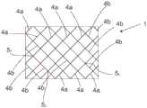
图1示意性地图示了根据一个实施方案的透明导电膜的正视图;Figure 1 schematically illustrates a front view of a transparent conductive film according to one embodiment;
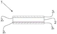
图2示意性地图示了根据一个实施方案的透明导电膜的截面图;Figure 2 schematically illustrates a cross-sectional view of a transparent conductive film according to one embodiment;
图3a示意性地图示了根据一个实施方案的透明导电膜的截面图;Figure 3a schematically illustrates a cross-sectional view of a transparent conductive film according to one embodiment;
图3b示意性地图示了根据一个实施方案的透明导电膜的截面图;Figure 3b schematically illustrates a cross-sectional view of a transparent conductive film according to one embodiment;
图4a示意性地图示了根据一个实施方案的透明导电膜的截面图;Figure 4a schematically illustrates a cross-sectional view of a transparent conductive film according to one embodiment;
图4b示意性地图示了图4a所示的透明导电膜的正视图;Figure 4b schematically illustrates a front view of the transparent conductive film shown in Figure 4a;
图5a图示了根据一个实施方案的包括透明导体材料,被图案化为具有第一电极的第一图案的第一透明层;Figure 5a illustrates a first transparent layer comprising a transparent conductor material, patterned into a first pattern having a first electrode, according to one embodiment;
图5b图示了根据一个实施方案的包括透明导体材料,被图案化为具有第二电极的第二图案和第二无源间隙区域的第二透明层;Figure 5b illustrates a second transparent layer comprising a transparent conductor material, patterned into a second pattern having a second electrode and a second passive gap region, according to one embodiment;
图5c图示了根据一个实施方案的当图5a的包括透明导体材料的第一透明层和图5b的包括导体材料的第二透明层一个布置在另一个上时的情况;Figure 5c illustrates the situation when the first transparent layer comprising a transparent conductor material of Figure 5a and the second transparent layer comprising a conductor material of Figure 5b are disposed one on top of the other, according to one embodiment;
图6a-6c示意性地图示了第一间隙区域和第二间隙区域的透明导体材料的覆盖逐渐降低;Figures 6a-6c schematically illustrate the gradual decrease in coverage of the transparent conductor material of the first gap region and the second gap region;
图7a示意性地图示了根据一个实施方案的透明导电膜的正视图;以及Figure 7a schematically illustrates a front view of a transparent conductive film according to one embodiment; and
图7b示意性地图示了如图7a所示的透明导电膜的截面图。Fig. 7b schematically illustrates a cross-sectional view of the transparent conductive film as shown in Fig. 7a.
具体实施方式Detailed ways
本申请涉及一种具有观察区的透明导电膜,其中该透明导电膜包括:The present application relates to a transparent conductive film having a viewing area, wherein the transparent conductive film includes:
至少一个透明基膜,其具有第一侧和与第一侧相对的第二侧;at least one transparent base film having a first side and a second side opposite the first side;
在观察区中,在至少一个透明基膜上设置的-第一透明层,其包括透明导体材料,被图案化为具有第一电极的第一图案和任选地与第一电极的第一图案分开的至少一个第一无源间隙区域,和In the viewing area, disposed on at least one transparent base film - a first transparent layer comprising a transparent conductor material, patterned with a first pattern of a first electrode and optionally with a first pattern of the first electrode separated by at least one first passive gap region, and
-第二透明层,其包括透明导体材料,被图案化为具有第二电极的第二图案和任选地与第二电极的第二图案分开的至少一个第二无源间隙区域;- a second transparent layer comprising a transparent conductor material, patterned with a second pattern of second electrodes and optionally at least one second passive gap region separated from the second pattern of second electrodes;
其中第一透明层和第二透明层在竖直方向上一个布置在另一个上,使得第一透明层的透明导体材料和第二透明层的透明导体材料形成wherein the first transparent layer and the second transparent layer are arranged one above the other in the vertical direction, so that the transparent conductor material of the first transparent layer and the transparent conductor material of the second transparent layer are formed
-至少一个交叉区域,在该交叉区域处,当从基本上垂直于至少一个透明基膜的第一侧或第二侧的方向观察时,第一透明层的透明导体材料和第二透明层的透明导体材料看起来至少部分重叠,和- at least one intersection area at which, when viewed from a direction substantially perpendicular to the first side or the second side of the at least one transparent base film, the difference between the transparent conductor material of the first transparent layer and the second transparent layer the transparent conductor material appears to overlap at least partially, and
-至少一个不重叠区域,在该不重叠区域处,第一透明层的透明导体材料和第二透明层的透明导体材料看起来不重叠;以及其中- at least one non-overlapping region at which the transparent conductor material of the first transparent layer and the transparent conductor material of the second transparent layer do not appear to overlap; and wherein
透射通过第一透明层的透明导体材料和第二透明层的透明导体材料的可见光的总百分比在整个观察区上基本相同。The total percentage of visible light transmitted through the transparent conductor material of the first transparent layer and the transparent conductor material of the second transparent layer is substantially the same over the entire viewing area.
本申请涉及一种具有观察区的透明导电膜,其中该透明导电膜包括:The present application relates to a transparent conductive film having a viewing area, wherein the transparent conductive film includes:
至少一个透明基膜,其具有第一侧和与第一侧相对的第二侧;at least one transparent base film having a first side and a second side opposite the first side;
在观察区中,在至少一个透明基膜上设置的In the viewing area, at least one transparent base film is provided with
-第一透明层,其包括透明导体材料,被图案化为具有第一电极的第一图案和任选地与第一电极的第一图案分开的至少一个第一无源间隙区域,和- a first transparent layer comprising a transparent conductor material, patterned with a first pattern of first electrodes and optionally at least one first passive gap region separated from the first pattern of first electrodes, and
-第二透明层,其包括透明导体材料,被图案化为具有第二电极的第二图案和任选地与第二电极的第二图案分开的至少一个第二无源间隙区域;- a second transparent layer comprising a transparent conductor material, patterned with a second pattern of second electrodes and optionally at least one second passive gap region separated from the second pattern of second electrodes;
其中第一透明层和第二透明层在竖直方向上一个布置在另一个上,使得第一透明层的透明导体材料和第二透明层的透明导体材料形成wherein the first transparent layer and the second transparent layer are arranged one above the other in the vertical direction, so that the transparent conductor material of the first transparent layer and the transparent conductor material of the second transparent layer are formed
-至少一个交叉区域,在该交叉区域处,当从基本上垂直于至少一个透明基膜的第一侧或第二侧的方向观察时,第一透明层的透明导体材料和第二透明层的透明导体材料看起来至少部分重叠,和- at least one intersection area at which, when viewed from a direction substantially perpendicular to the first side or the second side of the at least one transparent base film, the difference between the transparent conductor material of the first transparent layer and the second transparent layer the transparent conductor material appears to overlap at least partially, and
-至少一个不重叠区域,在该不重叠区域处,第一透明层的透明导体材料和第二透明层的透明导体材料看起来不重叠;以及- at least one non-overlapping region at which the transparent conductor material of the first transparent layer and the transparent conductor material of the second transparent layer do not appear to overlap; and
其中将第一透明层和第二透明层中的至少一个的透明导体材料在至少一个交叉区域处的覆盖降低至低于第一透明层或第二透明层的透明导体材料在第一透明层的透明导体材料和第二透明层的透明导体材料看起来不重叠的至少一个不重叠区域处的覆盖,使得透射通过第一透明层的透明导体材料和第二透明层的透明导体材料的可见光的总百分比在整个观察区上基本相同。wherein the coverage of the transparent conductor material of at least one of the first transparent layer and the second transparent layer at the at least one intersection region is reduced to be lower than the coverage of the transparent conductor material of the first transparent layer or the second transparent layer at the first transparent layer Coverage at at least one non-overlapping region where the transparent conductor material and the transparent conductor material of the second transparent layer do not appear to overlap, such that the total amount of visible light transmitted through the transparent conductor material of the first transparent layer and the transparent conductor material of the second transparent layer The percentages are essentially the same over the entire viewing area.
在一个实施方案中,透射通过第一透明层的透明导体材料和第二透明层的透明导体材料的可见光的总百分比在整个透明导电膜上保持基本相同。In one embodiment, the total percentage of visible light transmitted through the transparent conductor material of the first transparent layer and the transparent conductor material of the second transparent layer remains substantially the same throughout the transparent conductive film.
本申请还涉及一种用于制备具有观察区的透明导电膜的方法,其中该方法包括:The present application also relates to a method for preparing a transparent conductive film having a viewing area, wherein the method comprises:
提供至少一个透明基膜,该透明基膜具有第一侧和与第一侧相对的第二侧;providing at least one transparent base film having a first side and a second side opposite the first side;
在观察区中,在至少一个透明基膜上设置In the viewing area, disposed on at least one transparent base film
-第一透明层,其包括透明导体材料,被图案化为具有第一电极的第一图案和任选地与第一电极的第一图案分开的至少一个第一无源间隙区域,和- a first transparent layer comprising a transparent conductor material, patterned with a first pattern of first electrodes and optionally at least one first passive gap region separated from the first pattern of first electrodes, and
-第二透明层,其包括透明导体材料,被图案化为具有第二电极的第二图案和任选地与第二电极的第二图案分开的至少一个第二无源间隙区域;- a second transparent layer comprising a transparent conductor material, patterned with a second pattern of second electrodes and optionally at least one second passive gap region separated from the second pattern of second electrodes;
其中第一透明层和第二透明层在竖直方向上一个布置在另一个上,使得第一透明层的透明导体材料和第二透明层的透明导体材料形成wherein the first transparent layer and the second transparent layer are arranged one above the other in the vertical direction, so that the transparent conductor material of the first transparent layer and the transparent conductor material of the second transparent layer are formed
-至少一个交叉区域,在该交叉区域处,当从基本上垂直于至少一个透明基膜的第一侧或第二侧的方向观察时,第一透明层的透明导体材料和第二透明层的透明导体材料看起来至少部分重叠,和- at least one intersection area at which, when viewed from a direction substantially perpendicular to the first side or the second side of the at least one transparent base film, the difference between the transparent conductor material of the first transparent layer and the second transparent layer the transparent conductor material appears to overlap at least partially, and
-至少一个不重叠区域,在该不重叠区域处,第一透明层的透明导体材料和第二透明层的透明导体材料看起来不重叠;- at least one non-overlapping region at which the transparent conductor material of the first transparent layer and the transparent conductor material of the second transparent layer do not appear to overlap;
其中调整第一透明层和第二透明层中的至少一个的透明导体材料在至少一个交叉区域处的覆盖,使得透射通过第一透明层的透明导体材料和第二透明层的透明导体材料的可见光的总百分比在整个观察区上基本相同。wherein the coverage of the transparent conductor material of at least one of the first transparent layer and the second transparent layer at the at least one intersection area is adjusted such that visible light is transmitted through the transparent conductor material of the first transparent layer and the transparent conductor material of the second transparent layer The total percentage of is essentially the same over the entire viewing area.
本申请还涉及一种用于制备具有观察区的透明导电膜的方法,其中该方法包括:The present application also relates to a method for preparing a transparent conductive film having a viewing area, wherein the method comprises:
提供至少一个透明基膜,其具有第一侧和与第一侧相对的第二侧;providing at least one transparent base film having a first side and a second side opposite the first side;
在观察区中,在至少一个透明基膜上设置In the viewing area, disposed on at least one transparent base film
-第一透明层,其包括透明导体材料,被图案化为具有第一电极的第一图案和任选地与第一电极的第一图案分开的至少一个第一无源间隙区域,和- a first transparent layer comprising a transparent conductor material, patterned with a first pattern of first electrodes and optionally at least one first passive gap region separated from the first pattern of first electrodes, and
-第二透明层,其包括透明导体材料,被图案化为具有第二电极的第二图案和任选地与第二电极的第二图案分开的至少一个第二无源间隙区域;- a second transparent layer comprising a transparent conductor material, patterned with a second pattern of second electrodes and optionally at least one second passive gap region separated from the second pattern of second electrodes;
其中第一透明层和第二透明层在竖直方向上一个布置在另一个上,使得第一透明层的透明导体材料和第二透明层的透明导体材料形成wherein the first transparent layer and the second transparent layer are arranged one above the other in the vertical direction, so that the transparent conductor material of the first transparent layer and the transparent conductor material of the second transparent layer are formed
-至少一个交叉区域,在该交叉区域处,当从基本上垂直于至少一个透明基膜的第一侧或第二侧的方向观察时,第一透明层的透明导体材料和第二透明层的透明导体材料看起来至少部分重叠,和- at least one intersection area at which, when viewed from a direction substantially perpendicular to the first side or the second side of the at least one transparent base film, the difference between the transparent conductor material of the first transparent layer and the second transparent layer the transparent conductor material appears to overlap at least partially, and
-至少一个不重叠区域,在该不重叠区域处,第一透明层的透明导体材料和第二透明层的透明导体材料看起来不重叠;- at least one non-overlapping region at which the transparent conductor material of the first transparent layer and the transparent conductor material of the second transparent layer do not appear to overlap;
其中降低第一透明层和第二透明层中的至少一个的透明导体材料在至少一个交叉区域处的覆盖,使得透射通过第一透明层的透明导体材料和第二透明层的透明导体材料的可见光的总百分比在整个观察区上基本相同。wherein the coverage of the transparent conductor material of at least one of the first transparent layer and the second transparent layer at at least one intersection area is reduced so that visible light passing through the transparent conductor material of the first transparent layer and the transparent conductor material of the second transparent layer is transmitted The total percentage of is essentially the same over the entire viewing area.
在一个实施方案中,执行该方法以增加透明导电膜的透明度。In one embodiment, the method is performed to increase the transparency of the transparent conductive film.
在一个实施方案中,降低第一透明层和第二透明层中的至少一个的透明导体材料在至少一个交叉区域处的覆盖,使得透射通过第一透明层的透明导体材料和第二透明层的透明导体材料的可见光的总百分比在整个观察区上基本相同。In one embodiment, the coverage of the transparent conductor material of at least one of the first transparent layer and the second transparent layer is reduced at at least one intersection area such that the transmission through the transparent conductor material of the first transparent layer and the second transparent layer The total percentage of visible light of the transparent conductor material is substantially the same over the entire viewing area.
在一个实施方案中,第一透明层和第二透明层中的至少一个的透明导体材料在至少一个交叉区域处的覆盖相比于所述透明层的透明导体材料在至少一个不重叠区域处的覆盖降低。即,透明层的透明导体材料在至少一个交叉区域处的覆盖可以相比于同一透明层的透明导体材料在至少一个不重叠区域处的覆盖降低。In one embodiment, the coverage of the transparent conductor material of at least one of the first transparent layer and the second transparent layer at at least one intersection area is compared to the coverage of the transparent conductor material of the transparent layer at at least one non-overlapping area Coverage is reduced. That is, the coverage of the transparent conductor material of the transparent layer at the at least one intersecting region may be reduced compared to the coverage of the transparent conductor material of the same transparent layer at the at least one non-overlapping region.
本申请还涉及一种触摸感测设备,其包括如本申请中定义的透明导电膜或如本申请中定义的触敏膜。The application also relates to a touch sensing device comprising a transparent conductive film as defined in this application or a touch sensitive film as defined in this application.
本申请还涉及如本申请中定义的透明导电膜在光伏系统中、在加热应用中、在电流导体中、在显示系统中、在显示电极中、在照明系统中、在灯开关中或在光控膜中的用途。The application also relates to transparent conductive films as defined in this application in photovoltaic systems, in heating applications, in current conductors, in display systems, in display electrodes, in lighting systems, in light switches or in light Use in control membranes.
本申请还涉及如本申请中定义的触摸感测设备在光伏系统中、在加热应用中、在电流导体中、在显示系统中、在显示电极中、在照明系统中、在灯开关中或在光控膜中的用途。The application also relates to a touch sensing device as defined in this application in photovoltaic systems, in heating applications, in current conductors, in display systems, in display electrodes, in lighting systems, in light switches or in Uses in light control films.
除非另有说明,否则在本说明书中应将表述“观察区”理解为是指在透明导电膜的横向方向上观察或定义的预定区域或区。在一个实施方案中,观察区覆盖透明导电膜的面积的至少50%或至少60%或至少70%或至少80%或至少90%。Unless otherwise stated, the expression "observation area" should be understood in this specification to mean a predetermined area or area observed or defined in the transverse direction of the transparent conductive film. In one embodiment, the viewing area covers at least 50% or at least 60% or at least 70% or at least 80% or at least 90% of the area of the transparent conductive film.
除非另有说明,否则在本说明书中应将透射的可见光的总百分比“基本相同”的表述理解为是指透射的可见光的总百分比在整个观察区中可以不完全相同,而是透射的可见光的总百分比在整个观察区内可以发生变化。在一个实施方案中,透射通过第一透明层的透明导体材料和第二透明层的透明导体材料的可见光的总百分比在整个观察区上峰到峰变化至多5个百分点单位、或至多3个百分点单位、或0.05至5个百分点单位、或0.05至3个百分点单位、或0.05至1个百分点单位。优选地,与不重叠区域相比,在交叉区域处透射通过透明导体材料的可见光的百分比之间可能只有微小的偏差。但是,在第一透明层的电极图案和/或至少一个无源间隙区域内和/或在第二透明层的电极图案和/或至少一个无源间隙区域内可能存在小缝隙,其中透射的可见光的总百分比可能偏离超出上面的变化范围。但是,这些缝隙的尺寸使得在所讨论的透明导电膜的应用的通常观察距离处,透射率的偏差对于人眼是不可见的。这样的观察距离在不同的应用中可能不同。在一个实施方案中,观察距离是10-100cm或20-100cm,或30-100cm或50-100cm或60-300cm。换句话说,这些缝隙的尺寸可以低于人眼的平均分辨率。在一个实施方案中,这种缝隙的宽度是2-1000μm、或2-500μm、或2-50μm、或50-500μm。在一个实施方案中,第一透明层的透明导体材料和/或第二透明层的透明导体材料包括一个或多个缝隙,其宽度为2-1000μm、或2-500μm、或2-50μm,或50-500μm。Unless otherwise stated, the expression "substantially the same" in the total percentage of visible light transmitted should be understood in this specification to mean that the total percentage of visible light transmitted may not be exactly the same throughout the viewing area, but is The total percentage can vary throughout the viewing area. In one embodiment, the total percentage of visible light transmitted through the transparent conductor material of the first transparent layer and the transparent conductor material of the second transparent layer varies peak-to-peak by at most 5 percent units, or at most 3 percent across the viewing area Units, or 0.05 to 5 percent units, or 0.05 to 3 percent units, or 0.05 to 1 percent units. Preferably, there may be only a slight deviation between the percentages of visible light transmitted through the transparent conductor material at the intersection areas compared to the non-overlapping areas. However, there may be small gaps within the electrode pattern and/or at least one passive gap region of the first transparent layer and/or within the electrode pattern and/or at least one passive gap region of the second transparent layer, where visible light is transmitted The total percentage of may deviate beyond the above variation range. However, the dimensions of these gaps are such that at the usual viewing distances for the application of the transparent conductive film in question, deviations in transmittance are not visible to the human eye. Such viewing distances may vary in different applications. In one embodiment, the viewing distance is 10-100 cm or 20-100 cm, or 30-100 cm or 50-100 cm or 60-300 cm. In other words, the size of these slits can be lower than the average resolution of the human eye. In one embodiment, the width of such a slit is 2-1000 μm, or 2-500 μm, or 2-50 μm, or 50-500 μm. In one embodiment, the transparent conductor material of the first transparent layer and/or the transparent conductor material of the second transparent layer includes one or more slits having a width of 2-1000 μm, or 2-500 μm, or 2-50 μm, or 50-500μm.
在用于对角线小于15”的小型器具(诸如可穿戴设备、移动电话、平板电脑、笔记本电脑、汽车信息显示器或仪表板)的如触摸传感器、显示电极或灯开关的应用中,观察距离可以是例如20–100cm。在用于大面积监视器或电视的如触摸传感器、显示电极或灯开关的应用中,观察距离可以是例如60-300cm。在如触摸传感器、显示电极、灯开关、电流导体或例如窗户或挡风玻璃上的加热器元件的应用中,观察距离可以是例如30-100cm。In applications such as touch sensors, display electrodes or light switches for small appliances with a diagonal of less than 15" (such as wearables, mobile phones, tablets, laptops, automotive information displays or dashboards), viewing distance Can be eg 20-100cm. In applications such as touch sensors, display electrodes or light switches for large area monitors or televisions, the viewing distance can be eg 60-300cm. In applications such as touch sensors, display electrodes, light switches, In applications such as current conductors or heater elements such as on windows or windshields, the viewing distance may be, for example, 30-100 cm.
除非另有说明,否则在本说明书中应将表述“交叉区域”理解为是指当从基本上垂直于至少一个透明基膜的第一侧或第二侧的方向观察时第一透明层的透明导体材料和第二透明层的透明导体材料至少部分重叠的区域。即,当第一透明层和第二透明层在竖直方向上一个布置在另一个上时,第一透明层的透明导体材料和第二透明层的透明导体材料可以形成至少一个交叉区域。Unless otherwise stated, the expression "intersection region" should be understood in this specification to mean the transparency of the first transparent layer when viewed from a direction substantially perpendicular to the first side or the second side of the at least one transparent base film A region where the conductor material and the transparent conductor material of the second transparent layer at least partially overlap. That is, when the first transparent layer and the second transparent layer are arranged one above the other in the vertical direction, the transparent conductor material of the first transparent layer and the transparent conductor material of the second transparent layer may form at least one intersection area.
除非另有说明,否则在本说明书中应将表述“不重叠区域”理解为是指当从基本上垂直于至少一个透明基膜的第一侧或第二侧的方向观察时,第一透明层的透明导体材料和第二透明层的透明导体材料看起来不重叠的区域。即,当从基本上垂直于至少一个透明基膜的第一侧或第二侧的方向观察时,在不重叠区域处,透明导体材料可以存在于第一透明层或第二透明层中,但不同时存在于两者中。Unless otherwise stated, the expression "non-overlapping area" should be understood in this specification to mean the first transparent layer when viewed from a direction substantially perpendicular to the first or second side of the at least one transparent base film The area where the transparent conductor material of the second transparent layer and the transparent conductor material of the second transparent layer do not appear to overlap. That is, when viewed from a direction substantially perpendicular to the first side or the second side of the at least one transparent base film, at the non-overlapping regions, the transparent conductor material may be present in the first transparent layer or the second transparent layer, but not present in both.
除非另有说明,否则在本说明书中应将包括透明导体材料的透明层设置在透明基膜“上”的表述理解为是指透明层被设置或形成为位于透明基膜上或之上或至少部分地嵌入其中。透明基膜可以用作包括透明导体材料的透明层的载体或支撑结构。在一个实施方案中,透明基膜用作第一透明层和/或第二透明层的载体或支撑结构。Unless otherwise stated, in this specification the expression that a transparent layer comprising a transparent conductor material is disposed "on" a transparent base film shall be understood to mean that the transparent layer is disposed or formed to be disposed or formed on or on the transparent base film or at least partially embedded in it. The transparent base film can be used as a carrier or support structure for a transparent layer comprising a transparent conductor material. In one embodiment, the transparent base film is used as a carrier or support structure for the first transparent layer and/or the second transparent layer.
在本说明书中使用术语“包括”是指包含其后跟随的(一个或多个)特征或(一个或多个)动作,但不排除存在一个或多个其他特征或动作。还将理解的是,提到“一个(an)”项目是指一个或多个这些项目。The term "comprising" is used in this specification to mean the inclusion of the following feature(s) or action(s), but not excluding the presence of one or more other features or actions. It will also be understood that reference to "an" item refers to one or more of those items.
除非另有说明,否则在本说明书中应将表述“膜”理解为是指其横向尺寸实质上大于其厚度的结构。从这个意义上讲,膜可以被认为是“薄”结构。Unless otherwise stated, the expression "film" should be understood in this specification to mean a structure whose lateral dimensions are substantially greater than its thickness. In this sense, membranes can be considered as "thin" structures.
在一个实施方案中,透明基膜的由其横向尺寸形成的两侧形成第一侧和第二侧。In one embodiment, the two sides of the transparent base film formed by its lateral dimensions form the first side and the second side.
在一个实施方案中,透明导电膜的厚度为0.1μm-5mm,或20-500μm。In one embodiment, the thickness of the transparent conductive film is 0.1 μm-5 mm, or 20-500 μm.
除非另有说明,否则在本说明书中应将表述“电极”理解为是指能够提供和/或传输电压和/或电流的电导体。Unless otherwise stated, the expression "electrode" should be understood in this specification to mean an electrical conductor capable of providing and/or transmitting voltage and/or current.
除非另有说明,否则在本说明书中应将表述“透明”理解为是指导电膜及其部分和材料在所讨论的相关波长范围内的光学透明性。换句话说,“透明”材料或结构是指允许该相关波长的光或一般而言的电磁辐射通过其传播的材料或结构。相关的波长范围可以取决于要使用透明导电膜的应用。在一个实施方案中,相关波长范围是大约390至大约700nm的可见波长范围。Unless otherwise stated, the expression "transparent" should be understood in this specification to refer to the optical transparency of the conductive film and its parts and materials in the relevant wavelength range in question. In other words, a "transparent" material or structure refers to a material or structure that allows the propagation of light or electromagnetic radiation in general at that wavelength of interest therethrough. The relevant wavelength range may depend on the application for which the transparent conductive film is to be used. In one embodiment, the relevant wavelength range is the visible wavelength range of about 390 to about 700 nm.
另外,导电膜及其部分的透明度主要是指在导电膜的厚度方向上的透明度,因此为了是“透明的”,入射到导电膜或其一部分上的光能的足够部分应在厚度方向上传播通过它。这种足够的部分可以取决于要使用导电膜的应用。在一个实施方案中,在存在透明导体材料的位置处,这种部分是垂直入射到透明导电膜上的光能的20-99.99%。在一个实施方案中,所述透射率是20%或更高、或30%或更高、或40%或更高、或50%或更高、或60%或更高、或70%或更高、或80%或更高,90%或更高。可以根据标准JIS-K7361、ASTM D1003来测量透射率。通过透明导电膜或其部分传播或透射的可见光部分可以取决于透明导电膜改变可见光传输的能力,或者例如取决于其中使用的透明导体材料的类型。透光率的改变可能是由于例如损耗引起的吸收、散射和/或反射,或者透光率的某些其它改变(诸如颜色或清晰度的改变)。In addition, the transparency of the conductive film and parts thereof mainly refers to the transparency in the thickness direction of the conductive film, so in order to be "transparent", a sufficient part of the light energy incident on the conductive film or part thereof should propagate in the thickness direction pass it. Such a sufficient portion may depend on the application in which the conductive film is to be used. In one embodiment, where the transparent conductive material is present, this fraction is 20-99.99% of the light energy that is normally incident on the transparent conductive film. In one embodiment, the transmittance is 20% or higher, or 30% or higher, or 40% or higher, or 50% or higher, or 60% or higher, or 70% or higher High, or 80% or higher, 90% or higher. The transmittance can be measured according to standard JIS-K7361, ASTM D1003. The portion of visible light that propagates or transmits through the transparent conductive film, or portions thereof, may depend on the ability of the transparent conductive film to alter the transmission of visible light, or, for example, on the type of transparent conductor material used therein. The change in transmittance may be due to absorption, scattering and/or reflection due to loss, for example, or some other change in transmittance (such as a change in color or clarity).
在一个实施方案中,调整第一透明层和第二透明层中的至少一个的透明导体材料在至少一个交叉区域处的覆盖,使得透射通过第一透明层的透明导体材料和第二透明层的透明导体材料的可见光的总百分比在整个观察区上基本相同。In one embodiment, the coverage of the transparent conductor material of at least one of the first transparent layer and the second transparent layer at the at least one intersection region is adjusted such that the transmission through the transparent conductor material of the first transparent layer and the second transparent layer The total percentage of visible light of the transparent conductor material is substantially the same over the entire viewing area.
在一个实施方案中,通过减少透明导体材料在至少一个交叉区域处的预定量来调整第一透明层和/或第二透明层的透明导体材料的覆盖。In one embodiment, the coverage of the transparent conductor material of the first transparent layer and/or the second transparent layer is adjusted by reducing a predetermined amount of the transparent conductor material at at least one intersection area.
在一个实施方案中,降低第一透明层和第二透明层中的至少一个的透明导体材料在至少一个交叉区域处的覆盖至低于第一透明层或第二透明层的透明导体材料在第一透明层的透明导体材料和第二透明层的透明导体材料看起来不重叠的至少一个不重叠区域处的覆盖。In one embodiment, the coverage of the transparent conductor material of at least one of the first transparent layer and the second transparent layer is reduced at at least one intersection region to a level lower than that of the transparent conductor material of the first transparent layer or the second transparent layer at the first transparent layer or the second transparent layer. Overlay at at least one non-overlapping region where the transparent conductor material of one transparent layer and the transparent conductor material of the second transparent layer do not appear to overlap.
在一个实施方案中,第一透明层的透明导体材料和第二透明层的透明导体材料的总厚度在整个观察区上基本上是均匀的。In one embodiment, the total thickness of the transparent conductor material of the first transparent layer and the transparent conductor material of the second transparent layer is substantially uniform across the viewing area.
发明人发现,当降低第一透明层和第二透明层中的至少一个的透明导体材料在交叉区域处的覆盖时,可以改善透明导电膜对用户的视觉外观。当降低第一透明层和第二透明层中的至少一个的透明导体材料在交叉区域处的覆盖时,能够提供具有基本均匀的视觉外观的透明导电膜。当降低透明导体材料在第一透明层的透明导体材料和第二透明层的透明导体材料看起来至少部分重叠的部分处的覆盖时,可以增加可见光通过透明导电膜的传输。The inventors found that when the coverage of the transparent conductor material of at least one of the first transparent layer and the second transparent layer at the intersection area is reduced, the visual appearance of the transparent conductive film to the user can be improved. When the coverage of the transparent conductor material of at least one of the first transparent layer and the second transparent layer at the intersection area is reduced, a transparent conductive film having a substantially uniform visual appearance can be provided. Transmission of visible light through the transparent conductive film can be increased when the coverage of the transparent conductor material at the portion where the transparent conductor material of the first transparent layer and the transparent conductor material of the second transparent layer appear to at least partially overlap is reduced.
在一个实施方案中,第一透明层和第二透明层在竖直方向上一个布置在另一个上,使得第一电极和第二电极形成至少一个交叉区域,在该交叉区域处,当从基本上垂直于至少一个透明基膜的第一侧或第二侧的方向观察时,第一电极和第二电极看起来重叠。In one embodiment, the first transparent layer and the second transparent layer are arranged one above the other in the vertical direction, such that the first electrode and the second electrode form at least one intersection area at which, when viewed from substantially The first electrode and the second electrode appear to overlap when viewed in a direction perpendicular to the first side or the second side of the at least one transparent base film.
在一个实施方案中,降低第一电极和第二电极中的至少一个在一个或多个交叉区域处的形成该交叉区域的透明导体材料的覆盖至低于所述电极在交叉区域之外的透明导体材料的覆盖。In one embodiment, the coverage of at least one of the first electrode and the second electrode at one or more intersection regions of the transparent conductor material forming the intersection regions is reduced below the transparency of the electrodes outside the intersection regions Covering of conductor material.
在一个实施方案中,至少一个交叉区域包括至少一个交叉点,在该交叉点处,当从基本上垂直于至少一个透明基膜的第一侧或第二侧的方向观察时,第一电极和第二电极看起来彼此交叉。在一个实施方案中,至少一个交叉区域包括至少一个交叉点,在该交叉点处,当从基本上垂直于至少一个透明基膜的第一侧或第二侧的方向观察时,第一电极和第二电极看起来彼此交叉,并且其中降低第一电极和第二电极中的至少一个在至少一个交叉区域处的形成该交叉区域的透明导体材料的覆盖至低于所述电极在交叉区域之外的透明导体材料的覆盖。In one embodiment, the at least one intersection region includes at least one intersection point where, when viewed from a direction substantially perpendicular to the first side or the second side of the at least one transparent base film, the first electrode and the The second electrodes appear to cross each other. In one embodiment, the at least one intersection region includes at least one intersection point where, when viewed from a direction substantially perpendicular to the first side or the second side of the at least one transparent base film, the first electrode and the The second electrodes appear to intersect each other, and wherein the coverage of at least one of the first electrode and the second electrode at at least one intersection area of the transparent conductor material forming the intersection area is reduced below that of the electrodes outside the intersection area covered with transparent conductor material.
在一个实施方案中,第一透明层包括透明导体材料,被图案化为具有至少一个第一无源间隙区域。在一个实施方案中,第二透明层包括透明导体材料,被图案化为具有第二无源间隙区域。In one embodiment, the first transparent layer comprises a transparent conductor material, patterned to have at least one first passive gap region. In one embodiment, the second transparent layer includes a transparent conductive material, patterned to have a second passive gap region.
在一个实施方案中,第一透明层和第二透明层在竖直方向上一个布置在另一个上,使得第一透明层的透明导体材料和第二透明层的透明导体材料形成以下中的至少一个:In one embodiment, the first transparent layer and the second transparent layer are arranged one above the other in the vertical direction such that the transparent conductor material of the first transparent layer and the transparent conductor material of the second transparent layer form at least one of the following One:
-第一电极和第二电极看起来至少部分重叠的至少一个交叉区域;- at least one intersection area where the first electrode and the second electrode appear to overlap at least partially;
-第一电极和第二无源间隙区域看起来至少部分重叠的至少一个交叉区域;- at least one intersection area where the first electrode and the second passive gap area appear to at least partially overlap;
-第一无源间隙区域和第二无源间隙区域看起来至少部分重叠的至少一个交叉区域;- at least one intersection area in which the first non-active gap area and the second non-active gap area appear to overlap at least partially;
-第二电极和第一无源间隙区域看起来至少部分重叠的至少一个交叉区域。- at least one intersection area where the second electrode and the first passive gap area appear to overlap at least partially.
通常,当制备透明导电膜时,例如透明层的第一电极的第一图案和第二电极的第二图案形成预定数量的交叉点,当使用透明导体材料(诸如碳纳米管或碳纳米芽或在一定程度上吸收或折射光的其它导体材料)时,裸眼可以可视地看到这些交叉点。另外,当第一透明层和第二透明层在竖直方向上一个布置在另一个上时,例如,在将它们与(一个或多个)透明基膜粘合在一起的过程中,透明层的第一电极的第一图案和第二电极的第二图案也可以形成预定数量的交叉区域。由于粘合或层压工艺中的工艺变化,第一电极的第一图案和第二电极的第二图案在电极图案中除了第一电极的第一图案和第二电极的第二图案看起来彼此交叉的交叉点以外的其它部分中也可能看起来稍微重叠。发明人惊奇地发现,当使用在本申请中描述的方法时,可以制备具有仅由一层透明导体材料制成的视觉外观的透明导电膜。透明导电膜具有附加的效用,即,基本上没有通过例如电极或其它部分形成的图案可以被观看者裸眼实质可视地看到。发明人还发现,通常补偿由不同层的电极在交叉点处看起来彼此交叉这一事实所引起的视觉缺陷所需的任何附加填充材料可以从由本申请中所描述的方法制备的透明导电膜中省去。Generally, when a transparent conductive film is prepared, for example, the first pattern of the first electrode of the transparent layer and the second pattern of the second electrode form a predetermined number of intersections, when a transparent conductive material such as carbon nanotubes or carbon nanobuds or These intersections are visible to the naked eye when other conductor materials that absorb or refract light to some extent). In addition, when the first transparent layer and the second transparent layer are arranged one above the other in the vertical direction, for example, in the process of adhering them to the transparent base film(s), the transparent layer The first pattern of the first electrode and the second pattern of the second electrode may also form a predetermined number of intersecting regions. Due to process variations in the bonding or lamination process, the first pattern of the first electrode and the second pattern of the second electrode appear to each other in the electrode pattern except the first pattern of the first electrode and the second pattern of the second electrode There may also appear to be a slight overlap in other parts of the intersection other than the intersection. The inventors have surprisingly found that when using the methods described in this application, it is possible to produce transparent conductive films having the visual appearance of being made from only one layer of transparent conductive material. Transparent conductive films have the added effect that substantially no pattern formed by, for example, electrodes or other portions can be substantially visually seen by the naked eye of a viewer. The inventors have also discovered that any additional filler material typically required to compensate for visual defects caused by the fact that electrodes of different layers appear to cross each other at intersections can be derived from transparent conductive films prepared by the methods described in this application. Leave it out.
在一个实施方案中,透明导电膜缺少用于补偿由不同层的透明导体材料在交叉区域看起来重叠这一事实而引导的视觉缺陷的任何附加填充材料。在一个实施方案中,透明导电膜缺少用来补偿由于不同层的电极在交叉点处看起来彼此交叉这一事实而引起的视觉缺陷的任何附加填充材料。In one embodiment, the transparent conductive film lacks any additional filler material for compensating for visual defects induced by the fact that different layers of transparent conductor material appear to overlap in the intersection area. In one embodiment, the transparent conductive film lacks any additional filler material to compensate for visual defects caused by the fact that electrodes of different layers appear to cross each other at intersections.
在一个实施方案中,降低透明导体材料在一个或多个交叉区域处的覆盖范围。在一个实施方案中,降低透明导体材料在所有交叉区域处的覆盖。In one embodiment, the coverage of the transparent conductor material at one or more intersection regions is reduced. In one embodiment, the coverage of the transparent conductor material at all intersection areas is reduced.
“无源间隙区域”是指透明层的不被电连接的区域。无源间隙不与用于将透明层连接到外部电源的任何接触布置电连接。因此,从电气角度来看,这种无源间隙区域在其不参与透明导电膜的电操作的意义上是“无源”结构。"Passive gap region" refers to the region of the transparent layer that is not electrically connected. The passive gap is not electrically connected to any contact arrangement for connecting the transparent layer to an external power source. Therefore, from an electrical point of view, such a passive gap region is a "passive" structure in the sense that it does not participate in the electrical operation of the transparent conductive film.
无源间隙区域可以与电极图案分开。在电极图案与无源间隙区域之间可以仅存在具有例如几十微米的宽度的小缝隙。The passive gap region may be separated from the electrode pattern. There may only be small gaps with widths of, for example, tens of micrometers between the electrode pattern and the passive gap region.
在一个实施方案中,第一透明层包括透明导体材料,被图案化为具有至少一个第一无源间隙区域,但是第二透明层不具有第二无源间隙区域,反之亦然。In one embodiment, the first transparent layer comprises a transparent conductor material, patterned to have at least one first passive gap region, but the second transparent layer does not have the second passive gap region, and vice versa.
在一个实施方案中,第一透明层包括透明导体材料,被图案化为具有至少一个第一无源间隙区域,且第二透明层包括透明导体材料,被图案化为具有至少一个第二无源间隙区域,其中在观察区内,该至少一个第一无源间隙区域和该至少一个第二无源间隙区域看起来不重叠。In one embodiment, the first transparent layer includes a transparent conductor material, patterned with at least one first passive gap region, and the second transparent layer includes a transparent conductor material, patterned with at least one second passive gap A gap region, wherein the at least one first passive gap region and the at least one second passive gap region do not appear to overlap within the viewing area.
在一个实施方案中,第一透明层包括透明导体材料,被图案化为具有至少一个第一无源间隙区域,且第二透明层包括透明导体材料,被图案化为具有至少一个第二无源间隙区域,其中当从基本上垂直于至少一个透明基膜的第一侧或第二侧的方向观察时,该至少一个第一无源间隙区域和该至少一个第二无源间隙区域在至少一个交叉区域处看起来至少部分重叠。In one embodiment, the first transparent layer includes a transparent conductor material, patterned with at least one first passive gap region, and the second transparent layer includes a transparent conductor material, patterned with at least one second passive gap A gap region, wherein when viewed from a direction substantially perpendicular to the first side or the second side of the at least one transparent base film, the at least one first passive gap region and the at least one second passive gap region are in at least one The intersection area appears to overlap at least partially.
在一个实施方案中,通过降低透明导体材料在至少一个交叉区域处的预定量来调整第一无源间隙区域的透明导体材料和/或第二无源间隙区域的透明导体材料的覆盖。In one embodiment, the coverage of the transparent conductor material of the first passive gap region and/or the transparent conductor material of the second passive gap region is adjusted by reducing a predetermined amount of transparent conductor material at at least one intersection region.
在一个实施方案中,第一无源间隙区域具有第一边缘和与第一边缘相对的第二边缘,第二无源间隙区域具有第一边缘和与第一边缘相对的第二边缘,并且其中透明导体材料的覆盖从第一间隙区域的第一边缘到第二边缘逐渐或连续降低,而透明导体材料的覆盖从第二间隙区域的第二边缘到第一边缘以相反的方式逐渐或连续降低,反之亦然。In one embodiment, the first passive gap region has a first edge and a second edge opposite the first edge, the second passive gap region has a first edge and a second edge opposite the first edge, and wherein The coverage of the transparent conductor material decreases gradually or continuously from the first edge to the second edge of the first gap region, while the coverage of the transparent conductor material decreases gradually or continuously in the opposite manner from the second edge to the first edge of the second gap region ,vice versa.
在一个实施方案中,透射通过第一无源间隙区域的透明导体材料的可见光的百分比从第一边缘到第二边缘在大约100%至大约X%之间变化或从大约100%变化为大约X%,而透射通过第二无源间隙区域的透明导体材料的可见光的百分比从第一边缘到第二边缘在大约X%至大约100%之间变化或从大约X%变化为大约100%,反之亦然,其中X是透射通过第一透明层或第二透明层在交叉区域之外的透明导体材料的可见光的百分比。In one embodiment, the percentage of visible light transmitted through the transparent conductor material of the first passive gap region varies from about 100% to about X% or from about 100% to about X% from the first edge to the second edge %, while the percentage of visible light transmitted through the transparent conductor material of the second passive gap region varies from about X% to about 100% from the first edge to the second edge or from about X% to about 100%, and vice versa Likewise, where X is the percentage of visible light that is transmitted through the transparent conductor material of the first transparent layer or the second transparent layer outside the intersection area.
在一个实施方案中,在至少一个交叉区域处,透明导体材料的覆盖从第一透明层逐渐或连续地降低,而透明导体材料的覆盖从第二透明层以相反的方式逐渐或连续地降低,反之亦然。In one embodiment, the coverage of the transparent conductor material decreases gradually or continuously from the first transparent layer and the coverage of the transparent conductor material decreases gradually or continuously from the second transparent layer in the opposite manner at at least one intersection area, vice versa.
在一个实施方案中,降低一个透明层的透明导体材料在交叉区域处的覆盖,使得在交叉区域处透射通过所述透明层的透明导体材料的可见光的百分比在大约100%至大约X%之间或从大约100%至大约X%,其中X%是透射通过所述透明层在交叉区域之外的透明导体材料的可见光的百分比。在一个实施方案中,降低一个透明层的透明导体材料在交叉区域处的覆盖,使得在交叉区域处透射通过所述透明层的透明导体材料的可见光的百分比从透射通过所述透明层在交叉区域之外的透明导体材料的可见光的百分比逐渐增加到大约100%。In one embodiment, the coverage of the transparent conductor material of one transparent layer at the intersection area is reduced such that the percentage of visible light transmitted through the transparent conductor material of the transparent layer at the intersection area is between about 100% and about X% or From about 100% to about X%, where X% is the percentage of visible light transmitted through the transparent conductor material of the transparent layer outside the crossover region. In one embodiment, the coverage of the transparent conductor material of one transparent layer at the intersection area is reduced such that the percentage of visible light transmitted through the transparent conductor material of the transparent layer at the intersection area is reduced from transmission through the transparent layer at the intersection area The percentage of visible light outside the transparent conductor material gradually increases to approximately 100%.
通过逐渐降低透明导体材料在交叉区域处的覆盖,这可以在例如层压工艺中通过工艺变化而形成,从而第一电极的第一图案和第二电极的第二图案在电极图案的除交叉点之外的其它部分中也可能看起来略微重叠,这具有增加的效用,即降低能够裸眼识别这种重叠的可能性。This can be formed by process variation eg in a lamination process by gradually reducing the coverage of the transparent conductor material at the intersection areas so that the first pattern of the first electrode and the second pattern of the second electrode are at the intersection of the electrode patterns except at the intersection There may also appear to be a slight overlap in parts other than , which has the added utility of reducing the likelihood of being able to identify such an overlap with the naked eye.
在一个实施方案中,降低一个透明层的透明导体材料在交叉区域处的覆盖,使得透射通过所述透明层在交叉区域处的透明导体材料的可见光的百分比比透射通过所述透明层在交叉区域之外的透明导体材料的可见光的百分比高0.1–50个百分点单位、或0.1–20个百分点单位、或1–20个百分点单位。在一个实施方案中,降低一个透明层的透明导体材料在交叉点处的覆盖,使得透射通过所述透明层在交叉点处的透明导体材料的可见光的百分比比透射通过所述透明层在交叉点之外的透明导体材料的可见光的百分比高0.1–50%个百分点单位、或0.1–20个百分点单位、或1–20个百分点单位。In one embodiment, the coverage of the transparent conductor material of one transparent layer at the intersection area is reduced such that the percentage of visible light transmitted through the transparent conductor material of the transparent layer at the intersection area is higher than that transmitted through the transparent layer at the intersection area The percentage of visible light outside the transparent conductor material is 0.1-50 percentage points higher, or 0.1-20 percentage points, or 1-20 percentage points. In one embodiment, the coverage of the transparent conductor material of one transparent layer at the intersection is reduced such that the percentage of visible light transmitted through the transparent conductor material of the transparent layer at the intersection is greater than that transmitted through the transparent layer at the intersection The percentage of visible light outside the transparent conductor material is 0.1-50% higher, or 0.1-20 percentage points, or 1-20 percentage points.
在一个实施方案中,导电膜的至少一个透明基膜中的至少一个由介电材料制成,或者导电膜的所有透明基膜全部由介电材料制成。在一个实施方案中,透明基膜由透明玻璃或塑料材料形成。用于形成透明基膜的材料应当适于用作用于包括透明导体材料的透明层的基板。In one embodiment, at least one of the at least one transparent base film of the conductive film is made of a dielectric material, or all of the transparent base films of the conductive film are made of a dielectric material. In one embodiment, the transparent base film is formed from a transparent glass or plastic material. The material used to form the transparent base film should be suitable for use as a substrate for a transparent layer including a transparent conductor material.
在一个实施方案中,透明基膜的材料选自由钠钙玻璃、铝硅酸盐玻璃、硼硅酸盐玻璃及其任意组合组成的组。在一个实施方案中,透明基膜的材料选自由聚对苯二甲酸乙二醇酯(PET)、聚碳酸酯(PC)、聚甲基丙烯酸甲酯(PMMA)、环状烯烃共聚物(COP)、三乙酸酯(TAC)、环状烯烃共聚物(COC)、聚氯乙烯(PVC)、聚(2,6-萘二甲酸乙二醇酯)(PEN)、聚酰亚胺(PI)、聚丙烯(PP)、聚乙烯(PE)及其任意组合组成的组。但是,透明基膜的材料不限于这些示例。In one embodiment, the material of the transparent base film is selected from the group consisting of soda lime glass, aluminosilicate glass, borosilicate glass, and any combination thereof. In one embodiment, the material of the transparent base film is selected from polyethylene terephthalate (PET), polycarbonate (PC), polymethyl methacrylate (PMMA), cyclic olefin copolymer (COP) ), triacetate (TAC), cyclic olefin copolymer (COC), polyvinyl chloride (PVC), poly(2,6-ethylene naphthalate) (PEN), polyimide (PI) ), polypropylene (PP), polyethylene (PE) and any combination thereof. However, the material of the transparent base film is not limited to these examples.
在一个实施方案中,透明基膜的厚度为1-2000μm、或10-1000μm、或30-500μm、或50-300μm。但是,在一些应用中,透明基膜也可以更厚。In one embodiment, the thickness of the transparent base film is 1-2000 μm, or 10-1000 μm, or 30-500 μm, or 50-300 μm. However, in some applications, the transparent base film can also be thicker.
在一个实施方案中,第一电极的第一图案是与第二电极的第二图案相似的图案。在一个实施方案中,第一电极的第一图案是与第二电极的第二图案不同的图案。在一个实施方案中,第一电极的第一图案是X电极,第二电极的第二图案是Y电极,反之亦然。In one embodiment, the first pattern of the first electrode is a similar pattern to the second pattern of the second electrode. In one embodiment, the first pattern of the first electrode is a different pattern than the second pattern of the second electrode. In one embodiment, the first pattern of first electrodes is X electrodes and the second pattern of second electrodes is Y electrodes, and vice versa.
当第一透明层和第二透明层在竖直方向上一个布置在另一个上时,第一电极的第一图案和第二电极的第二图案可以形成适于具体应用的任何图案。在一个实施方案中,当第一透明层和第二透明层在竖直方向上一个布置在另一个上时,第一电极的第一图案和第二电极的第二图案可以形成菱形图案、雪花图案或网格形式的图案。在一个实施方案中,当第一透明层和第二透明层在竖直方向上一个布置在另一个上时,第一电极的第一图案和第二电极的第二图案可以形成菱形图案。When the first transparent layer and the second transparent layer are arranged one above the other in the vertical direction, the first pattern of the first electrode and the second pattern of the second electrode may form any pattern suitable for a specific application. In one embodiment, when the first transparent layer and the second transparent layer are arranged one on the other in a vertical direction, the first pattern of the first electrode and the second pattern of the second electrode may form a diamond pattern, a snowflake A pattern in the form of a pattern or grid. In one embodiment, when the first transparent layer and the second transparent layer are arranged one on the other in a vertical direction, the first pattern of the first electrode and the second pattern of the second electrode may form a diamond pattern.
在一个实施方案中,透明导电膜包括至少一个透明基膜。在一个实施方案中,透明导电膜包括一个透明基膜。在一个实施方案中,透明导电膜包括第一透明基膜和/或第二透明基膜。在一个实施方案中,透明导电膜包括第一透明基膜。在一个实施方案中,透明导电膜包括第一透明基膜和第二透明基膜。在一个实施方案中,透明导电膜包括多个透明基膜。In one embodiment, the transparent conductive film includes at least one transparent base film. In one embodiment, the transparent conductive film includes a transparent base film. In one embodiment, the transparent conductive film includes a first transparent base film and/or a second transparent base film. In one embodiment, the transparent conductive film includes a first transparent base film. In one embodiment, the transparent conductive film includes a first transparent base film and a second transparent base film. In one embodiment, the transparent conductive film includes a plurality of transparent base films.
在一个实施方案中,至少一个透明基膜包括一个透明基膜或由一个透明基膜组成。在一个实施方案中,至少一个透明基膜包括第一透明基膜和/或第二透明基膜或由第一透明基膜和/或第二透明基膜组成。在一个实施方案中,至少一个透明基膜包括第一透明基膜或由第一透明基膜组成。在一个实施方案中,至少一个透明基膜包括第一透明基膜和第二透明基膜或由第一透明基膜和第二透明基膜组成。在一个实施方案中,至少一个透明基膜包括多个透明基膜或由多个透明基膜组成。In one embodiment, the at least one transparent base film comprises or consists of a transparent base film. In one embodiment, the at least one transparent base film comprises or consists of the first transparent base film and/or the second transparent base film. In one embodiment, the at least one transparent base film includes or consists of the first transparent base film. In one embodiment, the at least one transparent base film includes or consists of a first transparent base film and a second transparent base film. In one embodiment, the at least one transparent base film includes or consists of a plurality of transparent base films.
在一个实施方案中,第一透明层设置在透明基膜的第一侧并且第二透明层设置在透明基膜的第二侧。In one embodiment, the first transparent layer is disposed on the first side of the transparent base film and the second transparent layer is disposed on the second side of the transparent base film.
在一个实施方案中,第一透明层设置在第一透明基膜上并且第二透明层设置在第二透明基膜上,其中第一透明层和第二透明层在竖直方向上一个布置在另一个上,使得第一透明基膜或第二透明基膜位于第一透明层和第二透明层之间。在一个实施方案中,第一透明层设置在第一透明基膜上并且第二透明层设置在第二透明基膜上,其中第一透明层和第二透明层在竖直方向上一个布置在另一个上,使得第一透明基膜或第二透明基膜位于第一透明层和第二透明层之间,但不是第一透明基膜和第二透明基膜两者同时位于第一透明层和第二透明层之间。In one embodiment, the first transparent layer is disposed on the first transparent base film and the second transparent layer is disposed on the second transparent base film, wherein the first transparent layer and the second transparent layer are disposed one above the other in the vertical direction On the other, the first transparent base film or the second transparent base film is positioned between the first transparent layer and the second transparent layer. In one embodiment, the first transparent layer is disposed on the first transparent base film and the second transparent layer is disposed on the second transparent base film, wherein the first transparent layer and the second transparent layer are disposed one above the other in the vertical direction On the other, either the first transparent base film or the second transparent base film is located between the first transparent layer and the second transparent layer, but not both the first transparent base film and the second transparent base film are located in the first transparent layer at the same time and the second transparent layer.
在一个实施方案中,第一透明层设置在透明基膜的第一侧并且第二透明层设置在透明基膜的相同第一侧,使得第一透明层和第二透明层在竖直方向上一个布置在另一个上,使得第一电极和第二电极在至少一个交叉区域处看起来重叠,而第一电极的第一图案和第二电极的第二图案原本实质上不重叠。在一个实施方案中,第一透明层设置在透明基膜的第一侧并且第二透明层设置在透明基膜的相同第一侧,使得第一透明层和第二透明层在竖直方向上一个布置在另一个上,使得第一电极和第二电极在预定数量的交叉点处看起来彼此交叉,而第一电极的第一图案和第二电极的第二图案原本实质上不重叠。在这个上下文中,除非另有说明,否则在本说明书中应当理解术语“原本实质上不重叠”,使得内涵是保持第一电极的第一图案和第二电极的第二图案在除它们看起来重叠的交叉点以外的其它部分中保持彼此分开。但是,由于工艺变化,在电极图案的其它部分中也会发生某些无意的重叠。In one embodiment, the first transparent layer is disposed on a first side of the transparent base film and the second transparent layer is disposed on the same first side of the transparent base film, such that the first transparent layer and the second transparent layer are in the vertical direction One is arranged over the other such that the first electrode and the second electrode appear to overlap at at least one intersection area, while the first pattern of the first electrode and the second pattern of the second electrode do not otherwise substantially overlap. In one embodiment, the first transparent layer is disposed on a first side of the transparent base film and the second transparent layer is disposed on the same first side of the transparent base film, such that the first transparent layer and the second transparent layer are in the vertical direction One is arranged over the other such that the first electrode and the second electrode appear to cross each other at a predetermined number of intersections, while the first pattern of the first electrode and the second pattern of the second electrode do not otherwise substantially overlap. In this context, unless otherwise stated, the term "original non-overlapping" should be understood in this specification, so that the connotation is to maintain the first pattern of the first electrode and the second pattern of the second electrode in addition to their appearance The parts other than the overlapping intersections remain separated from each other. However, due to process variations, some unintended overlap may also occur in other portions of the electrode pattern.
在一个实施方案中,透明导电膜包括粘合层。在一个实施方案中,粘合剂选自由丙烯酸粘合剂、硅粘合剂、交联聚合物及其任意组合组成的组。在一个实施方案中,粘合剂是光学透明粘合剂(OCA),诸如压敏光学透明粘合剂。In one embodiment, the transparent conductive film includes an adhesive layer. In one embodiment, the adhesive is selected from the group consisting of acrylic adhesives, silicone adhesives, cross-linked polymers, and any combination thereof. In one embodiment, the adhesive is an optically clear adhesive (OCA), such as a pressure sensitive optically clear adhesive.
在一个实施方案中,利用粘合剂将在第一透明基膜上设置第一透明层时形成的结构与在第二透明基膜上设置第二透明层时形成的结构粘合在一起。In one embodiment, the structure formed when the first transparent layer is disposed on the first transparent base film and the structure formed when the second transparent layer is disposed on the second transparent base film are bonded together using an adhesive.
在一个实施方案中,通过使用激光工艺、蚀刻工艺、直接印刷、机械工艺、燃烧工艺或其任意组合来降低透明导体材料的覆盖。在一个实施方案中,蚀刻工艺为光刻工艺。In one embodiment, the coverage of the transparent conductor material is reduced by using a laser process, an etching process, direct printing, a mechanical process, a combustion process, or any combination thereof. In one embodiment, the etching process is a photolithographic process.
在一个实施方案中,通过在交叉区域处的透明导体材料中形成至少一个斑点或至少一条线,或者通过减小交叉区域处的透明导体材料的厚度,来降低透明导体材料的覆盖。在一个实施方案中,通过减小在至少一个交叉点处的第一电极和第二电极中的至少一个的厚度来降低透明导体材料的覆盖。In one embodiment, the coverage of the transparent conductor material is reduced by forming at least one spot or at least one line in the transparent conductor material at the intersection area, or by reducing the thickness of the transparent conductor material at the intersection area. In one embodiment, the coverage of the transparent conductor material is reduced by reducing the thickness of at least one of the first electrode and the second electrode at at least one intersection.
在一个实施方案中,在将第一透明层和第二透明层一个布置在另一个上之前和/或之后,降低透明导体材料的覆盖。In one embodiment, the coverage of the transparent conductor material is reduced before and/or after the first transparent layer and the second transparent layer are disposed one over the other.
在一个实施方案中,通过移除预定量的透明导体材料来降低透明导体材料的覆盖。In one embodiment, the coverage of the transparent conductor material is reduced by removing a predetermined amount of the transparent conductor material.
在一个实施方案中,通过使第一电极和/或第二电极在交叉区域处,诸如在交叉点处变薄来降低透明导体材料的覆盖。在一个实施方案中,通过使第一电极和/或第二电极在交叉区域处(例如,在交叉点处)的厚度变薄,和/或通过使第一电极和/或第二电极在交叉区域处(例如,在交叉点处)具有更窄的宽度,来降低透明导体材料的覆盖。In one embodiment, the coverage of the transparent conductor material is reduced by thinning the first electrode and/or the second electrode at the intersection area, such as at the intersection. In one embodiment, by thinning the thickness of the first electrode and/or the second electrode at the intersection region (eg, at the intersection), and/or by thinning the first electrode and/or the second electrode at the intersection Areas (eg, at intersections) have narrower widths to reduce the coverage of the transparent conductor material.
在一个实施方案中,第一电极和第二电极中的至少一个在(一个或多个)交叉区域处的厚度较薄,使得第一电极和第二电极在(一个或多个)交叉区域处的总厚度基本上类似于第一电极和第二电极中的每个电极在(一个或多个)交叉区域之外的单独的厚度。在一个实施方案中,第一电极和第二电极中的至少一个在(一个或多个)交叉点处的厚度较薄,使得第一电极和第二电极在(一个或多个)交叉点处的总厚度基本上类似于第一电极和第二电极中的每个电极在(一个或多个)交叉点之外的单独的厚度。In one embodiment, at least one of the first electrode and the second electrode has a thinner thickness at the intersection area(s) such that the first electrode and the second electrode are at the intersection area(s) The total thickness of is substantially similar to the individual thickness of each of the first electrode and the second electrode outside the intersection area(s). In one embodiment, at least one of the first electrode and the second electrode has a thinner thickness at the intersection(s) such that the first electrode and the second electrode are at the intersection(s) The total thickness of is substantially similar to the individual thickness of each of the first and second electrodes outside the intersection(s).
在一个实施方案中,透明触敏膜为电阻式触敏膜。在一个实施方案中,透明触敏膜是电容式触敏膜。In one embodiment, the transparent touch sensitive film is a resistive touch sensitive film. In one embodiment, the transparent touch sensitive film is a capacitive touch sensitive film.
透明层包括透明导体材料,被图案化为具有电极图案和任选地与电极图案分开的至少一个无源间隙区域。因此,透明导体材料可以用于形成电极图案和无源间隙区域二者。透明导体材料可以包括任何适当的、足够透明的导体材料或这些材料的任意组合。The transparent layer includes a transparent conductive material, patterned with an electrode pattern and optionally at least one passive gap region separated from the electrode pattern. Thus, transparent conductor material can be used to form both the electrode pattern and the passive gap region. The transparent conductor material may comprise any suitable sufficiently transparent conductor material or any combination of these materials.
在一个实施方案中,透明导体材料包括导电高纵横比分子结构(HARMS)网络或由导电高纵横比分子结构(HARMS)网络组成。在一个实施方案中,透明导体材料包括导电高纵横比分子结构(HARMS)网络。In one embodiment, the transparent conductor material comprises or consists of a network of conductive high aspect ratio molecular structures (HARMS). In one embodiment, the transparent conductor material includes a conductive high aspect ratio molecular structure (HARMS) network.
导电“HARMS”或“HARM结构”是指导电性“纳米结构”,即,具有一个或多个纳米级特征尺寸(即,小于或等于大约100纳米)的结构。“高纵横比”是指导电结构在两个垂直方向上的尺寸处于明显不同的数量级。例如,纳米结构的长度可以比其厚度和/或宽度高数十倍或数百倍。在HARMS网络中,大量的所述纳米结构彼此互连以形成电互连分子的网络。从宏观尺度上考虑,HARMS网络形成固体单片材料,其中各个分子结构是不定向的或非取向的,即,基本上是随机取向或取向的。可以以具有合理电阻率的透明薄层的形式制备各种类型的HARMS网络。Conductive "HARMS" or "HARM structure" refers to conductive "nanostructures," ie, structures having one or more nanoscale feature sizes (ie, less than or equal to about 100 nanometers). "High aspect ratio" means that the dimensions of the conductive structures in the two perpendicular directions are of significantly different orders of magnitude. For example, the length of a nanostructure can be tens or hundreds of times greater than its thickness and/or width. In a HARMS network, a large number of the nanostructures are interconnected to each other to form a network of electrically interconnected molecules. Considered on a macroscopic scale, HARMS networks form solid monolithic materials in which the individual molecular structures are non-oriented or non-oriented, ie, substantially randomly oriented or oriented. Various types of HARMS networks can be prepared in the form of transparent thin layers with reasonable resistivity.
在一个实施方案中,导电HARM结构包括金属纳米线,诸如银纳米线。In one embodiment, the conductive HARM structure includes metal nanowires, such as silver nanowires.
在一个实施方案中,导电HARM网络包括碳纳米结构。在一个实施方案中,碳纳米结构包括碳纳米管、碳纳米芽、碳纳米带或其任意组合。在一个实施方案中,碳纳米结构包括碳纳米芽,即,碳纳米芽分子。碳纳米芽或碳纳米芽分子具有共价键合至管状碳分子的侧面的富勒烯或类富勒烯分子。碳纳米结构,尤其是碳纳米芽,从电学、光学(透明度)和机械学(稳健性与柔韧性和/或可变形性结合)的观点来看都可以提供优点。In one embodiment, the conductive HARM network includes carbon nanostructures. In one embodiment, the carbon nanostructures include carbon nanotubes, carbon nanobuds, carbon nanoribbons, or any combination thereof. In one embodiment, the carbon nanostructures comprise carbon nanobuds, ie, carbon nanobud molecules. Carbon nanobuds or carbon nanobud molecules have fullerene or fullerene-like molecules covalently bonded to the sides of the tubular carbon molecule. Carbon nanostructures, especially carbon nanobuds, can offer advantages from an electrical, optical (transparency) and mechanical (robustness combined with flexibility and/or deformability) point of view.
在一个实施方案中,透明导体材料包括透明导电氧化物或由透明导电氧化物组成。在一个实施方案中,透明导体材料包括以下或由以下组成:氧化铟锡(ITO)、氧化锌、铝掺杂的氧化锌(AZO)、氟掺杂的氧化锡(FTO)或它们的任意组合。在一个实施方案中,透明导体材料包括透明导电氧化物。在一个实施方案中,透明导电氧化物是氧化铟锡(ITO)、氧化锌、铝掺杂的氧化锌(AZO)、氟掺杂的氧化锡(FTO)或其任意组合。在一个实施方案中,透明导电氧化物掺杂有掺杂剂,诸如氟。In one embodiment, the transparent conductor material includes or consists of a transparent conductive oxide. In one embodiment, the transparent conductor material comprises or consists of indium tin oxide (ITO), zinc oxide, aluminum doped zinc oxide (AZO), fluorine doped tin oxide (FTO), or any combination thereof . In one embodiment, the transparent conductor material includes a transparent conductive oxide. In one embodiment, the transparent conductive oxide is indium tin oxide (ITO), zinc oxide, aluminum doped zinc oxide (AZO), fluorine doped tin oxide (FTO), or any combination thereof. In one embodiment, the transparent conductive oxide is doped with a dopant, such as fluorine.
在一个实施方案中,透明导体材料包括以下或由以下组成:石墨烯、银纳米线、聚(3,4-乙烯二氧噻吩)PEDOT、聚(3,4-乙烯二氧噻吩)聚苯乙烯磺酸盐PEDOT:PSS、聚苯胺、金属网导体或它们的任意组合。在一个实施方案中,透明导体材料包括石墨烯、银纳米线、聚(3,4-乙烯二氧噻吩)PEDOT、聚(3,4-乙烯二氧噻吩)聚苯乙烯磺酸盐PEDOT:PSS、聚苯胺、金属网导体或它们的任意组合。In one embodiment, the transparent conductor material comprises or consists of the following: graphene, silver nanowires, poly(3,4-ethylenedioxythiophene)PEDOT, poly(3,4-ethylenedioxythiophene)polystyrene Sulfonate PEDOT: PSS, polyaniline, metal mesh conductors or any combination thereof. In one embodiment, the transparent conductor material includes graphene, silver nanowires, poly(3,4-ethylenedioxythiophene) PEDOT, poly(3,4-ethylenedioxythiophene) polystyrene sulfonate PEDOT:PSS , polyaniline, metal mesh conductors, or any combination thereof.
每个透明层的厚度可以根据透明导电材料的特性(尤其是其电阻率或电导率)来设计。例如,在透明导体材料包括碳纳米结构的情况下,透明层的厚度可以是例如1-1000nm。在一个实施方案中,透明层的厚度是0.1-1000nm、或10–800nm,或50–300nm。在一个实施方案中,透明层的厚度是10-50nm、或50-100nm、或150-300nm、或500-1000nm。但是,如基于本说明书所理解的,考虑到透明导体材料在至少一个交叉区域处的覆盖可能减小,单独的透明层的厚度可以在不同部分之间变化。The thickness of each transparent layer can be designed according to the properties of the transparent conductive material, especially its resistivity or conductivity. For example, where the transparent conductor material includes carbon nanostructures, the thickness of the transparent layer may be, for example, 1-1000 nm. In one embodiment, the thickness of the transparent layer is 0.1-1000 nm, or 10-800 nm, or 50-300 nm. In one embodiment, the thickness of the transparent layer is 10-50 nm, or 50-100 nm, or 150-300 nm, or 500-1000 nm. However, as understood based on this specification, the thickness of the individual transparent layers may vary from portion to portion, taking into account that the coverage of the transparent conductor material at the at least one intersection region may be reduced.
在一个实施方案中,提供至少一个透明基膜包括利用预先形成和制造的完整的透明基膜。可以首先通过任何适当的工艺制备这种透明基膜以将其用于制备透明导电膜的方法中。在一个实施方案中,提供至少一个透明基膜包括制造透明基膜,作为用于制备透明导电膜的方法的一部分。In one embodiment, providing at least one transparent base film includes utilizing a pre-formed and fabricated complete transparent base film. Such a transparent base film may first be prepared by any suitable process for use in a method of preparing a transparent conductive film. In one embodiment, providing at least one transparent base film includes making the transparent base film as part of a method for making a transparent conductive film.
在一个实施方案中,通过在透明基膜上沉积透明导体材料来设置包括透明导体材料的透明层。In one embodiment, the transparent layer comprising the transparent conductor material is provided by depositing the transparent conductor material on the transparent base film.
根据透明层的材料,可以使用现有技术中存在的各种程序来设置透明层。例如,可以在真空条件下通过溅射来沉积ITO。PEDOT或银纳米线可以例如通过印刷形成。金属网可以例如通过印刷或电镀或通过任何其它适当的方法形成。Depending on the material of the transparent layer, the transparent layer can be provided using various procedures existing in the prior art. For example, ITO can be deposited by sputtering under vacuum conditions. PEDOT or silver nanowires can be formed, for example, by printing. The metal mesh can be formed, for example, by printing or electroplating or by any other suitable method.
在透明导体材料包括碳纳米结构(诸如碳纳米芽分子)的情况下,可以例如通过使用从气相或从液体中过滤、在力场中沉积或使用喷涂或旋转干燥从溶液沉积的通常已知的方法来执行沉积。碳纳米芽分子可以例如使用WO 2007/057501中公开的方法合成,并且例如通过例如电泳或热泳的辅助或通过Nasibulin等人在“Multifunctional Free-StandingSingle-Walled 20Carbon Nanotube Films”,ACS NANO,第5卷,第4期,3214-3221,2011中所描述的方法例如直接从气溶胶流沉积在透明基膜上。Where the transparent conductor material comprises carbon nanostructures, such as carbon nanobud molecules, it may be possible, for example, by using commonly known methods such as filtration from the gas phase or from a liquid, deposition in a force field, or deposition from solution using spraying or spin drying. method to perform deposition. Carbon nanobud molecules can be synthesized, for example, using the methods disclosed in WO 2007/057501 and, for example, aided by e.g. electrophoresis or thermophoresis or by Nasibulin et al. in "Multifunctional Free-StandingSingle-Walled 20 Carbon Nanotube Films", ACS NANO, p. 5 The method described in Vol. 4, 3214-3221, 2011, for example, is deposited directly from an aerosol stream on a transparent base film.
在一个实施方案中,透明导体材料沉积在至少一个透明基膜上。在一个实施方案中,透明导体材料以图案沉积在至少一个透明膜上。In one embodiment, the transparent conductor material is deposited on at least one transparent base film. In one embodiment, the transparent conductor material is deposited on the at least one transparent film in a pattern.
在一个实施方案中,包括透明导体材料的透明层被图案化为具有电极图案和任选地至少一个与电极图案分开的无源间隙区域。电极图案和任选的至少一个无源间隙区域可以与在透明基膜上形成或沉积透明层同时或在其之后设置。在一个实施方案中,透明层直接以形成电极和任选地无源间隙区域的图案形成或沉积在透明基膜上。In one embodiment, a transparent layer comprising a transparent conductor material is patterned with an electrode pattern and optionally at least one passive gap region separate from the electrode pattern. The electrode pattern and optionally the at least one passive gap region may be provided at the same time as or after the formation or deposition of the transparent layer on the transparent base film. In one embodiment, the transparent layer is formed or deposited directly on the transparent base film in a pattern that forms the electrodes and optionally the passive gap regions.
在所述图案化中,可以使用各种工艺。在一个实施方案中,使用激光工艺、蚀刻工艺、直接印刷、机械工艺、燃烧工艺或其任意组合用于形成电极图案和任选地至少一个无源间隙区域。在一个实施方案中,激光工艺是激光烧蚀。在一个实施方案中,蚀刻工艺是光刻工艺。In the patterning, various processes can be used. In one embodiment, a laser process, etching process, direct printing, mechanical process, combustion process, or any combination thereof is used for forming the electrode pattern and optionally at least one passive gap region. In one embodiment, the laser process is laser ablation. In one embodiment, the etching process is a photolithographic process.
在一个实施方案中,透明导电膜包括或设置有至少一个附加层。在一个实施方案中,在透明导电膜上设置保护层。附加层可以包括底板或盖板。底板和盖板中的任何一个可以包括透明塑料材料(诸如丙烯酸酯或PC或它们的多层层压体)或者玻璃材料(诸如浮法玻璃(包含SiO2、Na2O、CaO、MgO)、钙钠玻璃、或铝硅酸盐或硼硅酸盐玻璃),或由此类玻璃和/或塑料材料制成的层压体。典型的汽车安全玻璃可以包括两个浮法玻璃片,其间嵌有塑料,例如聚乙烯醇缩丁醛(PVB)。In one embodiment, the transparent conductive film includes or is provided with at least one additional layer. In one embodiment, a protective layer is provided on the transparent conductive film. Additional layers may include a base plate or a cover plate. Either of the base plate and the cover plate may comprise a transparent plastic material such as acrylate or PC or their multilayer laminates, or a glass material such as float glass (including SiO2 , Na2 O, CaO, MgO), soda lime glass, or aluminosilicate or borosilicate glass), or laminates made of such glass and/or plastic materials. A typical automotive safety glass may include two float glass sheets with plastic, such as polyvinyl butyral (PVB), embedded between them.
在一个实施方案中,透明导电膜形成为柔性结构,以允许其在至少一个方向上沿着三维表面弯曲,优选可逆且重复地弯曲。在一个实施方案中,透明导电膜在至少两个方向上可同时弯曲。根据用于制备透明导电膜的材料,透明导电膜可以弯曲的最小曲率半径可以例如在0.5mm至3或10mm的范围内。对于包括碳纳米结构(诸如碳纳米芽)的透明层,可以实现该最小曲率半径,而对于其它材料,最低可能的曲率半径可以更高。In one embodiment, the transparent conductive film is formed as a flexible structure to allow it to bend, preferably reversibly and repeatedly, along a three-dimensional surface in at least one direction. In one embodiment, the transparent conductive film is simultaneously bendable in at least two directions. Depending on the material used to prepare the transparent conductive film, the minimum radius of curvature to which the transparent conductive film can be bent may be, for example, in the range of 0.5 mm to 3 or 10 mm. This minimum radius of curvature may be achieved for transparent layers comprising carbon nanostructures such as carbon nanobuds, while for other materials the lowest possible radius of curvature may be higher.
在一个实施方案中,透明导电膜形成为可变形的结构,以允许透明导电膜沿着三维表面变形。所述变形可以基于例如透明导电膜的可拉伸性,并且可以例如通过使用热成型来执行。柔韧性和/或变形性可以具有附加的效用,即使得能够将透明导电膜用作弯曲的或一般而言三维形状的结构,诸如圆顶形状的结构。In one embodiment, the transparent conductive film is formed into a deformable structure to allow the transparent conductive film to deform along a three-dimensional surface. The deformation may be based, for example, on the stretchability of the transparent conductive film, and may be performed, for example, by using thermoforming. Flexibility and/or deformability may have the added utility of enabling the use of transparent conductive films as curved or generally three-dimensional shaped structures, such as dome-shaped structures.
在一个实施方案中,透明导电膜已经进行了热成型和/或注射成型。在一个实施方案中,该方法包括使透明导电膜经受注射成型和/或热成型。在一个实施方案中,透明导电膜被形成为具有三维形状。In one embodiment, the transparent conductive film has been thermoformed and/or injection molded. In one embodiment, the method includes subjecting the transparent conductive film to injection molding and/or thermoforming. In one embodiment, the transparent conductive film is formed to have a three-dimensional shape.
将理解的是,在本申请中描述的益处和优点可以涉及一个实施方案或可以涉及若干实施方案。这些实施方案不限于解决了任何或所有所述问题的实施方案或具有任何或所有所述益处和优点的实施方案。It will be appreciated that the benefits and advantages described in this application may relate to one embodiment or may relate to several embodiments. These embodiments are not limited to those that solve any or all of the stated problems or those that have any or all of the stated benefits and advantages.
上文描述的实施方案可以彼此任意组合使用。这些实施方案中的几个可以组合在一起以形成另外的实施方案。本申请涉及的透明导电膜、方法、触摸感测设备或用途可以包括上述实施方案中的至少一个。The embodiments described above can be used in any combination with each other. Several of these embodiments can be combined together to form additional embodiments. Transparent conductive films, methods, touch sensing devices, or uses to which the present application relates may include at least one of the above-described embodiments.
通过本说明书中定义的方法制备的透明导电膜具有增加的效用,即具有改善的视觉外观,因为第一透明层的透明导体材料和第二透明层的透明导体材料的重叠形成的交叉区域可能是人的裸眼基本上不可见的。The transparent conductive film prepared by the method defined in this specification has increased utility, ie, improved visual appearance, because the overlapping area formed by the overlapping of the transparent conductor material of the first transparent layer and the transparent conductor material of the second transparent layer may be Basically invisible to the naked eye.
用于制备透明导电膜的方法具有增加的效用,即使得能够制备透明导电膜,而无需使用为了降低例如由电极形成的可见图案的影响而通常需要的透明导体材料的附加填充材料。The method for making transparent conductive films has the added utility of enabling transparent conductive films to be made without the use of additional filler materials such as transparent conductor materials that are typically required to reduce the effect of visible patterns formed by electrodes, for example.
与没有调整或降低透明导体材料在交叉区域处的覆盖的类似透明导电膜相比,透明导电膜具有增加的效用,即在整个膜上具有合适的透明性而不牺牲视觉均匀性。Compared to similar transparent conductive films that do not adjust or reduce the coverage of the transparent conductor material at the intersection areas, the transparent conductive films have the increased utility of having suitable transparency throughout the film without sacrificing visual uniformity.
用于制备透明导电膜的方法具有增加的效用,即使得能够在不牺牲透明性的情况下制备导电性提高的透明导电膜,反之亦然。Methods for making transparent conductive films have increased utility, ie, enable the production of transparent conductive films with increased conductivity without sacrificing transparency, and vice versa.
实施例Example
现在将详细参考所描述的实施方案,其实施例在附图中示出。Reference will now be made in detail to the described embodiments, examples of which are illustrated in the accompanying drawings.
以下描述以使得本领域技术人员基于本公开能够利用该方法、透明导电膜和触敏设备的细节公开了一些实施方案。并非详细讨论了这些实施方案的所有步骤,因为基于本说明书,许多步骤对于本领域技术人员而言是明显的。The following description discloses some embodiments to enable those skilled in the art based on the present disclosure to utilize the details of the method, transparent conductive film, and touch-sensitive device. Not all steps of these embodiments have been discussed in detail, as many steps will be apparent to those skilled in the art based on this description.
为了简单起见,在重复部件的情况下,在以下示例性实施方案中将维持项目编号。For simplicity, in the case of repeating components, item numbers will be maintained in the following exemplary embodiments.
图1示意性地图示了根据本说明书中描述的一个实施方案的透明导电膜1的正视图。从图1中,可以看到当第一透明层和第二透明层彼此之间一个布置在另一个上使得第一电极4a的第一图案和第二电极4b的第二图案形成预定数量的交叉区域或交叉点51,52…5n时第一电极4a的第一图案和第二电极4b的第二图案形成的预定图案,在该交叉点51,52…5n处,当从基本上垂直于至少一个透明基膜的第一侧或第二侧的方向观察时,第一透明层的电极4a和第二透明层的电极4b看起来彼此交叉。需要强调的是,在图1中,电极形成的图案以黑色突出显示以更好地图示该实施方案。但是,实际上,电极可以是透明的并且基本上是裸眼不可见的。在图1中,并非第一电极与第二电极交叉时形成的所有交叉点都用附图标记指示,但是显然,指示51,52…5n表示在预定图案中形成的所有交叉点。FIG. 1 schematically illustrates a front view of a transparent
图2示意性地图示了根据一个实施方案的透明导电膜1的截面图,其中具有第一电极的第一图案的第一透明层31设置(例如沉积)在透明基膜2的第一侧2a,并且具有第二电极的第二图案的第二透明层32设置(例如沉积)在透明基膜2的第二侧2b。图2没有图示由形成至少一个交叉区域和至少一个不重叠区域的第一透明层的透明导体材料和第二透明层的透明导体材料引起的第一透明层和第二透明层的厚度变化或差异。FIG. 2 schematically illustrates a cross-sectional view of a transparent
图3a示意性地图示了根据一个实施方案的透明导电膜1的截面图,其中具有第一电极的第一图案的第一透明层31形成在第一透明基膜21上,例如形成在第一透明基膜21的第一侧上,且具有第二电极的第二图案的第二透明层32形成在第二透明基膜22上,例如形成在第二透明基膜22的第一侧上。然后,将在透明基膜上设置透明层时形成的这两种结构一个布置在另一个上。图3b示意性地图示了根据图3a的实施方案的透明导电膜的截面图,不同之处在于使用粘合剂6将包括透明基膜上的透明层的上述结构粘合在一起。图3a和图3b没有图示由形成至少一个交叉区域和至少一个不重叠区域的第一透明层的透明导体材料和第二透明层的透明导体材料引起的第一透明层和第二透明层的厚度变化或差异。Figure 3a schematically illustrates a cross-sectional view of a transparent
图4a示意性地图示了根据一个实施方案的透明导电膜1的截面图,其中第一透明层31和第二透明层32均设置在透明基膜2的第一侧2a上。图4a没有图示由形成至少一个交叉区域和至少一个不重叠区域的第一透明层的透明导体材料和第二透明层的透明导体材料引起的第一透明层和第二透明层的厚度变化或差异。图4b示意性地图示了图4a中所示的透明导电膜的正视图,其中第一透明层和第二透明层彼此之间一个布置在另一个上,使得第一电极4a的第一图案和第二电极4b的第二图案在预定数量的交叉区域(例如,交叉点(51,52))处看起来彼此交叉,而第一电极的第一图案和第二电极的第二图案原本实质上不重叠。FIG. 4a schematically illustrates a cross-sectional view of a transparent
图5a图示了根据一个实施方案的包括透明导体材料,被图案化为具有第一电极(例如,X电极)的第一图案的第一透明层。图5b图示了根据一个实施方案的包括透明导体材料,被图案化为具有第二电极(例如,Y电极)的第二图案和第二无源间隙区域的第二透明层。图5c图示了根据一个实施方案的当图5a的包括透明导体材料的第一透明层和图5b的包括透明导体材料的第二透明层一个布置在另一个上时的情况。5a illustrates a first transparent layer comprising a transparent conductor material, patterned into a first pattern having a first electrode (eg, an X electrode), according to one embodiment. Figure 5b illustrates a second transparent layer comprising a transparent conductor material, patterned into a second pattern with a second electrode (eg, a Y electrode) and a second passive gap region, according to one embodiment. Figure 5c illustrates the situation when the first transparent layer comprising a transparent conductor material of Figure 5a and the second transparent layer comprising a transparent conductor material of Figure 5b are arranged one on top of the other, according to one embodiment.
图6a示意性地图示了可以如何调整透明导体材料的覆盖。在图6a-6c中,图示了在第一透明层和第二透明层在竖直方向上一个布置在另一个上的情况下可以至少部分重叠的第一无源间隙区域6a和第二无源间隙区域6b的透明导体材料的覆盖如何的实施方案。图6a示意性地图示了第一无源间隙区域6a的透明导体材料的覆盖如何可以从第一无源间隙区域的第一边缘6a1到第一无源间隙区域的第二边缘6a2逐渐降低。图6b示意性地图示了第二无源间隙区域6b的透明导体材料的覆盖如何可以相比于第一无源间隙区域6a以相反的方式从第二无源间隙区域6b的第一边缘6b1到第二边缘6b2逐渐降低。图6c示意性地图示了当第一透明层和第二透明层一个布置在另一个上使得在该实施方案中第一无源间隙区域和第二无源间隙区域看起来至少部分重叠的情况。Figure 6a schematically illustrates how the coverage of the transparent conductor material can be adjusted. In Figures 6a-6c, the first
图7a示意性地图示了根据一个实施方案的透明导电膜的正视图,并且图7b示意性地图示了图7a的透明导电膜的一部分的截面图,即图7a和图7b所示的透明导电膜从点A到点B的截面图。在图7a中,呈现了透明导电膜的观察区7。透明导电膜可以延伸超出所呈现的观察区7。图7a所示的实施方案包括被图案化为具有第一电极4a的第一图案的透明导体材料的第一透明层和被图案化为具有第二电极4b的第二图案的透明导体材料的第二透明层。在图7a的实施方案中,第一电极4a的第一图案和第二电极4b的第二图案形成四个交叉区域51、52、53、54,在这些交叉区域,电极看起来彼此交叉。另外,在图7a的实施方案中,第一电极4a的第一图案和第二电极4b的第二图案还形成不重叠区域,其中的两个在图7a中用附图标记指示,即,81、82。在这些不重叠区域中,第一电极的第一图案和第二电极的第二图案可以实质上不重叠。Figure 7a schematically illustrates a front view of a transparent conductive film according to one embodiment, and Figure 7b schematically illustrates a cross-sectional view of a portion of the transparent conductive film of Figure 7a, ie the transparent conductive film shown in Figures 7a and 7b Cross-sectional view of the membrane from point A to point B. In Figure 7a, the viewing area 7 of the transparent conductive film is presented. The transparent conductive film may extend beyond the presented viewing area 7 . The embodiment shown in Figure 7a includes a first transparent layer of transparent conductor material patterned into a first pattern of
如图7b中所示,第一透明层还包括与第一电极的第一图案分开的透明导体材料的第一无源间隙区域,并且第二透明层还包括与第二电极的第二图案分开的透明导体材料的第二无源间隙区域。这些无源间隙区域看起来至少部分重叠,从而形成另外的交叉区域;其中之一在图7a中用附图标记5n表示。As shown in Figure 7b, the first transparent layer further includes a first passive gap region of transparent conductor material separated from the first pattern of the first electrode, and the second transparent layer further includes a second pattern of the second electrode separated from the second transparent layer a second passive gap region of transparent conductor material. These passive gap regions appear to overlap at least partially, forming additional intersection regions; one of whichis indicated by
在图7b中,图示了从图7a的实施方式的点A到点B的截面图。在图7b中,可以看到如下所述的实施方案:其中提供了一个透明基膜2,并且在观察区内具有包括透明导体材料,被图案化为具有第一电极4a的第一图案和与第一电极的第一图案分开的第一无源间隙区域6a的第一透明层,和包括透明导体材料,被图案化为具有第二电极4b的第二图案和与第二电极的第二图案分开的第二无源间隙区域6b的第二透明层。第一透明层和第二透明层在竖直方向上一个布置在另一个上,使得第一透明层的透明导体材料4a、6a和第二透明层的透明导体材料4b、6b形成交叉区域5n和两个不重叠区域81、82,在该交叉区域5n处,当从基本上垂直于透明基膜2的第一侧或第二侧的方向观察时,第一透明层的透明导体材料6a和第二透明层的透明导体材料6b看起来重叠,在该不重叠区域81、82处,第一透明层的透明导体材料4a和第二透明层的透明导体材料4b看起来不重叠。图7b示意性地图示了与第一透明层和第二透明层的透明导体材料在不重叠区域处的覆盖相比,减小第一透明层和第二透明层的透明导体材料在交叉区域处的覆盖的一种方式。In Fig. 7b, a cross-sectional view from point A to point B of the embodiment of Fig. 7a is illustrated. In Fig. 7b, an embodiment can be seen as described in which a
实施例1–制备透明导电膜Example 1 - Preparation of Transparent Conductive Film
在这个实施例中,通过以下程序制备透明导电膜:In this example, a transparent conductive film was prepared by the following procedure:
在这个实施例中,首先提供两个不同的透明基膜,即第一透明基膜和第二透明基膜。这两个透明基膜都是聚碳酸酯(PC)膜。In this embodiment, two different transparent base films are first provided, namely a first transparent base film and a second transparent base film. Both transparent base films are polycarbonate (PC) films.
然后,在第一透明基膜上形成包括透明导体材料的第一透明层,并且在第二透明基膜上形成包括透明导体材料的第二透明层。Then, a first transparent layer including a transparent conductor material is formed on the first transparent base film, and a second transparent layer including a transparent conductor material is formed on the second transparent base film.
在这个实施例中,透明导体材料包括碳纳米芽分子。可以根据WO 2007/057501A1中公开的合成工艺的细节,可以合成碳纳米芽分子。将碳纳米芽分子沉积在两个聚碳酸酯膜的每一个上,以在其上形成包括透明导体材料的透明层。In this embodiment, the transparent conductor material includes carbon nanobud molecules. Carbon nanobud molecules can be synthesized according to the details of the synthesis process disclosed in WO 2007/057501A1. Carbon nanobud molecules were deposited on each of the two polycarbonate films to form thereon a transparent layer comprising a transparent conductor material.
在将碳纳米芽分子沉积在两个聚碳酸酯膜的每一个上之后,执行图案化为在第一透明层中形成第一电极的第一图案并且在第二透明层中形成第二电极的第二图案。使用激光烧蚀(Delphi LES-G5,IR波长纳秒脉冲激光)分别制作第一电极的第一图案和第二电极的第二图案。使用以下激光参数用于制作第一电极的第一图案和第二电极的第二图案:功率:24,频率250,标记速度(mm/s):2000,计数:1。After the carbon nanobud molecules are deposited on each of the two polycarbonate films, patterning to form a first pattern of a first electrode in the first transparent layer and a second electrode in the second transparent layer is performed Second pattern. Laser ablation (Delphi LES-G5, IR wavelength nanosecond pulsed laser) was used to make the first pattern of the first electrode and the second pattern of the second electrode, respectively. The following laser parameters were used for making the first pattern of the first electrode and the second pattern of the second electrode: power: 24, frequency 250, marking speed (mm/s): 2000, counts: 1.
在为透明层提供预定的电极图案的同时,在预定的交叉点(其在稍后的阶段当将第一透明层和第二透明层一个布置在另一个上时形成,使得形成的第一电极和第二电极在这些交叉点处看起来彼此交叉)处,通过使用与用于制作第一电极的第一图案和第二电极的第二图案相同的激光烧蚀工艺,还使透明导体材料的覆盖从这些交叉点处的第一电极和第二电极降低。将透明导体材料的覆盖降低到低于交叉点之外。使用以下激光参数来降低第一电极和第二电极的透明导体材料在交叉点处的覆盖:Delphi LES-G5,IR波长纳秒脉冲激光,功率:20,频率250,标记速度(mm/s):2000,计数:1While providing the transparent layer with a predetermined electrode pattern, at predetermined intersections (which are formed at a later stage when the first transparent layer and the second transparent layer are arranged one on the other, so that the first electrode is formed and the second electrode appear to cross each other at these intersections), by using the same laser ablation process used to make the first pattern of the first electrode and the second pattern of the second electrode, the transparent conductor material is also Coverage decreases from the first and second electrodes at these intersections. Reduce the coverage of the transparent conductor material below the point of intersection. The following laser parameters were used to reduce the coverage of the transparent conductor material of the first electrode and the second electrode at the intersection: Delphi LES-G5, IR wavelength nanosecond pulsed laser, power: 20, frequency 250, marking speed (mm/s) : 2000, count: 1
因此,在第一透明基膜上设置了包括透明导体材料,被图案化为具有第一电极的第一图案的第一透明层,并且在第二透明基膜上设置了包括透明导体材料,被图案化为具有第二电极的第二图案的第二透明层。然后,将这两个结构一个布置在另一个上。Therefore, a first transparent layer comprising a transparent conductor material is provided on the first transparent base film, patterned into a first pattern having a first electrode, and a first transparent layer comprising a transparent conductor material is provided on the second transparent base film, which is A second transparent layer patterned into a second pattern with a second electrode. Then, the two structures are arranged one on top of the other.
在这个实施例中,透明导体材料的覆盖从交叉点处的第一电极和第二电极均减小了45面积%。因此,在交点处,被第一透明层的透明导体材料和第二透明层的透明导体材料吸收的可见光的总百分比从10%降低到7%。即使由不同层的透明导体材料形成,所形成的透明导电膜也具有仅由一层透明导体材料形成的视觉外观。尤其是,裸眼无法区分由第一电极的第一图案和第二电极的第二图案形成的交叉点。In this example, the coverage of the transparent conductor material is reduced by 45 area % from both the first and second electrodes at the intersection. Thus, at the intersection, the total percentage of visible light absorbed by the transparent conductor material of the first transparent layer and the transparent conductor material of the second transparent layer is reduced from 10% to 7%. Even if formed of different layers of transparent conductive material, the formed transparent conductive film has a visual appearance formed of only one layer of transparent conductive material. In particular, the naked eye cannot distinguish the intersection formed by the first pattern of the first electrode and the second pattern of the second electrode.
实施例2–制备透明导电膜Example 2 - Preparation of Transparent Conductive Film
在这个实施例中,通过以下程序制备透明导电膜:In this example, a transparent conductive film was prepared by the following procedure:
首先,如实施例1中所述,重复用于在第一透明基膜上设置包括透明导体材料的第一透明层和在第二透明基膜上设置包括透明导体材料的第二透明层的程序。First, as described in Example 1, the procedures for providing the first transparent layer including the transparent conductor material on the first transparent base film and the second transparent layer including the transparent conductor material on the second transparent base film are repeated .
在将碳纳米芽分子沉积在两个聚碳酸酯膜的每一个上之后,执行图案化为在第一透明层中形成第一电极的第一图案并且在第二透明层中形成第二电极的第二图案。在这个实施例中,通过以下光刻工艺形成第一电极的第一图案和第二电极的第二图案:首先,在碳纳米芽分子的沉积层上旋涂一层光致抗蚀剂材料,使其厚度大约为1μm。然后将具有预定图案的光掩模与透明基膜对准。然后通过光掩模中的开口使光致抗蚀剂暴露于UV光。光致抗蚀剂的暴露区域中的聚合物分子通过吸收UV光子而改变,使改变的光致抗蚀剂更易溶于显影液。然后通过整体浸入显影剂中来移除暴露的抗蚀剂。剩余的光致抗蚀剂用作用于蚀刻到透明层中的掩模层。然后使用酸蚀刻来移除包括透明导体材料(即碳纳米芽分子)的透明层的一部分,因此将图案转印到透明层,从而形成第一电极的第一图案和第二电极的第二图案。最后,通过使用丙酮溶剂将光致抗蚀剂洗掉。如以上针对实施例1所述,在这个实施例中,同样按照上述光刻程序来降低透明导体材料在交叉点处的材料覆盖。After the carbon nanobud molecules are deposited on each of the two polycarbonate films, patterning to form a first pattern of a first electrode in the first transparent layer and a second electrode in the second transparent layer is performed Second pattern. In this embodiment, the first pattern of the first electrode and the second pattern of the second electrode are formed by the following photolithography process: first, a layer of photoresist material is spin-coated on the deposited layer of carbon nanobud molecules, Make it about 1 μm thick. A photomask having a predetermined pattern is then aligned with the transparent base film. The photoresist is then exposed to UV light through openings in the photomask. The polymer molecules in the exposed areas of the photoresist are altered by absorbing UV photons, making the altered photoresist more soluble in the developer solution. The exposed resist is then removed by immersion of the bulk in a developer. The remaining photoresist serves as a mask layer for etching into the transparent layer. Acid etching is then used to remove a portion of the transparent layer comprising the transparent conductor material (ie, carbon nanobud molecules), thus transferring the pattern to the transparent layer, thereby forming a first pattern of the first electrode and a second pattern of the second electrode . Finally, the photoresist is washed away by using acetone solvent. As described above for
因此,在第一透明基膜上设置了包括透明导体材料,被图案化为具有第一电极的第一图案的第一透明层,并且在第二透明基膜上设置了包括透明导体材料,被图案化为具有第二电极的第二图案的第二透明层。然后,将这两个结构一个布置在另一个上。Therefore, a first transparent layer comprising a transparent conductor material is provided on the first transparent base film, patterned into a first pattern having a first electrode, and a first transparent layer comprising a transparent conductor material is provided on the second transparent base film, which is A second transparent layer patterned into a second pattern with a second electrode. Then, the two structures are arranged one on top of the other.
即使由不同层的透明导体材料形成,所形成的透明导电膜也具有仅由一层透明导体材料形成的视觉外观。尤其是,裸眼无法区分由第一电极的第一图案和第二电极的第二图案形成的交叉点。Even if formed of different layers of transparent conductive material, the formed transparent conductive film has a visual appearance formed of only one layer of transparent conductive material. In particular, the naked eye cannot distinguish the intersection formed by the first pattern of the first electrode and the second pattern of the second electrode.
需要注意的是,权利要求的实施方案不限于以上讨论的那些,而是在权利要求的范围内可以存在其它实施方案。It is noted that the embodiments of the claims are not limited to those discussed above, but other embodiments may exist within the scope of the claims.
Claims (19)
Translated fromChineseApplications Claiming Priority (3)
| Application Number | Priority Date | Filing Date | Title |
|---|---|---|---|
| FI20175595AFI20175595A7 (en) | 2017-06-22 | 2017-06-22 | A transparent conductive film |
| FI20175595 | 2017-06-22 | ||
| PCT/FI2018/050448WO2018234627A1 (en) | 2017-06-22 | 2018-06-13 | TRANSPARENT CONDUCTIVE FILM |
Publications (1)
| Publication Number | Publication Date |
|---|---|
| CN110770687Atrue CN110770687A (en) | 2020-02-07 |
Family
ID=64736872
Family Applications (1)
| Application Number | Title | Priority Date | Filing Date |
|---|---|---|---|
| CN201880041366.XAPendingCN110770687A (en) | 2017-06-22 | 2018-06-13 | Transparent conductive film |
Country Status (8)
| Country | Link |
|---|---|
| US (1) | US10932364B2 (en) |
| EP (1) | EP3642702A1 (en) |
| JP (1) | JP2020524841A (en) |
| KR (1) | KR20200020733A (en) |
| CN (1) | CN110770687A (en) |
| FI (1) | FI20175595A7 (en) |
| TW (1) | TW201904763A (en) |
| WO (1) | WO2018234627A1 (en) |
Cited By (1)
| Publication number | Priority date | Publication date | Assignee | Title |
|---|---|---|---|---|
| CN113427875A (en)* | 2021-07-09 | 2021-09-24 | 云南名博包装印刷有限公司 | Composite film with three-dimensional effect and manufacturing process thereof |
Families Citing this family (5)
| Publication number | Priority date | Publication date | Assignee | Title |
|---|---|---|---|---|
| FI128435B (en)* | 2018-05-09 | 2020-05-15 | Canatu Oy | An electrically conductive multilayer film |
| DE102019107358A1 (en) | 2019-03-22 | 2020-09-24 | Hib Trim Part Solutions Gmbh | Vehicle trim |
| CN113727838A (en)* | 2019-04-26 | 2021-11-30 | 柯尼卡美能达株式会社 | Transparent electrode and electronic device provided with same |
| KR102743259B1 (en)* | 2019-08-02 | 2024-12-16 | 삼성디스플레이 주식회사 | Light control film and display device comprising the same |
| FI20195798A1 (en) | 2019-09-23 | 2021-03-24 | Canatu Oy | LAYERED PRESSURE TREATMENT EQUIPMENT AND METHOD |
Citations (8)
| Publication number | Priority date | Publication date | Assignee | Title |
|---|---|---|---|---|
| CN101520708A (en)* | 2008-02-27 | 2009-09-02 | 株式会社日立显示器 | Display panel |
| US20110285641A1 (en)* | 2010-05-20 | 2011-11-24 | Unidisplay Inc. | Touch-sensing display panel and touch-sensing color filter substrate |
| CN103080876A (en)* | 2010-07-05 | 2013-05-01 | Dic株式会社 | Substrate with transparent conductive layer, manufacturing method thereof, transparent conductive film laminate for touch panel, touch panel |
| US20130162547A1 (en)* | 2011-12-27 | 2013-06-27 | Samsung Electro-Mechanics Co., Ltd. | Touch screen |
| US20140001018A1 (en)* | 2012-06-29 | 2014-01-02 | Lg Innotek Co., Ltd. | Touch window having improved electrode pattern structure |
| JP2014102547A (en)* | 2012-11-16 | 2014-06-05 | Shin Etsu Polymer Co Ltd | Conductive pattern-formed substrate, capacitive sensor sheet and method for manufacturing the same |
| CN105210015A (en)* | 2013-05-14 | 2015-12-30 | 卡纳图有限公司 | Flexible light emitting and blocking films |
| CN105637452A (en)* | 2013-10-18 | 2016-06-01 | 应用材料公司 | Transparent body for touch panel manufacturing method and system for manufacturing transparent body of touch screen panel |
Family Cites Families (5)
| Publication number | Priority date | Publication date | Assignee | Title |
|---|---|---|---|---|
| FI120195B (en) | 2005-11-16 | 2009-07-31 | Canatu Oy | Carbon nanotubes functionalized with covalently bonded fullerenes, process and apparatus for producing them, and composites thereof |
| US8723818B2 (en) | 2010-09-10 | 2014-05-13 | Atmel Corporation | Touch screen poly layer electrode distribution |
| US20120153970A1 (en) | 2010-12-21 | 2012-06-21 | Qualcomm Mems Technologies, Inc. | Capacitive touch sensing devices and methods of manufacturing thereof |
| US8773392B2 (en) | 2012-02-28 | 2014-07-08 | Eastman Kodak Company | Transparent touch-responsive capacitor with variable-pattern micro-wires |
| JP5813831B1 (en) | 2014-07-02 | 2015-11-17 | 日本航空電子工業株式会社 | Touch panel |
- 2017
- 2017-06-22FIFI20175595Apatent/FI20175595A7/ennot_activeApplication Discontinuation
- 2018
- 2018-06-13TWTW107120342Apatent/TW201904763A/enunknown
- 2018-06-13CNCN201880041366.XApatent/CN110770687A/enactivePending
- 2018-06-13USUS16/615,146patent/US10932364B2/enactiveActive
- 2018-06-13JPJP2019566788Apatent/JP2020524841A/enactivePending
- 2018-06-13WOPCT/FI2018/050448patent/WO2018234627A1/ennot_activeCeased
- 2018-06-13KRKR1020197038619Apatent/KR20200020733A/ennot_activeWithdrawn
- 2018-06-13EPEP18820975.3Apatent/EP3642702A1/ennot_activeWithdrawn
Patent Citations (8)
| Publication number | Priority date | Publication date | Assignee | Title |
|---|---|---|---|---|
| CN101520708A (en)* | 2008-02-27 | 2009-09-02 | 株式会社日立显示器 | Display panel |
| US20110285641A1 (en)* | 2010-05-20 | 2011-11-24 | Unidisplay Inc. | Touch-sensing display panel and touch-sensing color filter substrate |
| CN103080876A (en)* | 2010-07-05 | 2013-05-01 | Dic株式会社 | Substrate with transparent conductive layer, manufacturing method thereof, transparent conductive film laminate for touch panel, touch panel |
| US20130162547A1 (en)* | 2011-12-27 | 2013-06-27 | Samsung Electro-Mechanics Co., Ltd. | Touch screen |
| US20140001018A1 (en)* | 2012-06-29 | 2014-01-02 | Lg Innotek Co., Ltd. | Touch window having improved electrode pattern structure |
| JP2014102547A (en)* | 2012-11-16 | 2014-06-05 | Shin Etsu Polymer Co Ltd | Conductive pattern-formed substrate, capacitive sensor sheet and method for manufacturing the same |
| CN105210015A (en)* | 2013-05-14 | 2015-12-30 | 卡纳图有限公司 | Flexible light emitting and blocking films |
| CN105637452A (en)* | 2013-10-18 | 2016-06-01 | 应用材料公司 | Transparent body for touch panel manufacturing method and system for manufacturing transparent body of touch screen panel |
Cited By (1)
| Publication number | Priority date | Publication date | Assignee | Title |
|---|---|---|---|---|
| CN113427875A (en)* | 2021-07-09 | 2021-09-24 | 云南名博包装印刷有限公司 | Composite film with three-dimensional effect and manufacturing process thereof |
Also Published As
| Publication number | Publication date |
|---|---|
| US10932364B2 (en) | 2021-02-23 |
| FI20175595A1 (en) | 2018-12-23 |
| TW201904763A (en) | 2019-02-01 |
| JP2020524841A (en) | 2020-08-20 |
| WO2018234627A1 (en) | 2018-12-27 |
| EP3642702A1 (en) | 2020-04-29 |
| US20200174622A1 (en) | 2020-06-04 |
| KR20200020733A (en) | 2020-02-26 |
| FI20175595A7 (en) | 2018-12-23 |
Similar Documents
| Publication | Publication Date | Title |
|---|---|---|
| US10932364B2 (en) | Transparent conductive film | |
| US9941877B2 (en) | Electrode pattern of touch panel | |
| KR200476809Y1 (en) | Touch electrode device | |
| KR101103751B1 (en) | Touch screen panel with mesh type electrode pattern | |
| CN103415830A (en) | Touch panel, method for manufacturing the same, and liquid crystal display device including the touch panel | |
| CN106415462B (en) | touch window | |
| KR200479272Y1 (en) | Touch panel | |
| TW201428586A (en) | Touch panel | |
| CN106575187B (en) | touch window | |
| KR101956086B1 (en) | Touch panel, display and method of the same | |
| KR101555080B1 (en) | Touch sensor intergrated with a polarizer and display device comprising the same | |
| CN107533392A (en) | Touch window and display with touch window | |
| CN104881185A (en) | Touch panel and touch electrode structure thereof | |
| US9798426B2 (en) | Touch panel and method of manufacturing thereof | |
| US10228580B2 (en) | Touch panel | |
| TW201426445A (en) | Touch panel and touch-controlled display device | |
| CN103941896B (en) | Touch panel and touch display device | |
| KR20160141525A (en) | Touch panel | |
| CN103294314B (en) | A kind of capacitance touch screen with polarisation function | |
| TWM453196U (en) | Touch panel | |
| CN203786714U (en) | Touch panel and touch electrode structure thereof | |
| KR20150101847A (en) | Touch window and display with the same | |
| KR102303068B1 (en) | Touch window | |
| TWM458607U (en) | Touch member | |
| KR20170039391A (en) | Touch window |
Legal Events
| Date | Code | Title | Description |
|---|---|---|---|
| PB01 | Publication | ||
| PB01 | Publication | ||
| SE01 | Entry into force of request for substantive examination | ||
| SE01 | Entry into force of request for substantive examination | ||
| WD01 | Invention patent application deemed withdrawn after publication | ||
| WD01 | Invention patent application deemed withdrawn after publication | Application publication date:20200207 |