CN110769095A - Screen assemblies for electronic equipment and electronic equipment - Google Patents
Screen assemblies for electronic equipment and electronic equipmentDownload PDFInfo
- Publication number
- CN110769095A CN110769095ACN201910983586.0ACN201910983586ACN110769095ACN 110769095 ACN110769095 ACN 110769095ACN 201910983586 ACN201910983586 ACN 201910983586ACN 110769095 ACN110769095 ACN 110769095A
- Authority
- CN
- China
- Prior art keywords
- light
- hole
- camera
- inner ring
- ring edge
- Prior art date
- Legal status (The legal status is an assumption and is not a legal conclusion. Google has not performed a legal analysis and makes no representation as to the accuracy of the status listed.)
- Granted
Links
Images


Classifications
- G—PHYSICS
- G06—COMPUTING OR CALCULATING; COUNTING
- G06F—ELECTRIC DIGITAL DATA PROCESSING
- G06F1/00—Details not covered by groups G06F3/00 - G06F13/00 and G06F21/00
- G06F1/16—Constructional details or arrangements
- G06F1/1613—Constructional details or arrangements for portable computers
- G06F1/1633—Constructional details or arrangements of portable computers not specific to the type of enclosures covered by groups G06F1/1615 - G06F1/1626
- G06F1/1637—Details related to the display arrangement, including those related to the mounting of the display in the housing
- H—ELECTRICITY
- H04—ELECTRIC COMMUNICATION TECHNIQUE
- H04M—TELEPHONIC COMMUNICATION
- H04M1/00—Substation equipment, e.g. for use by subscribers
- H04M1/02—Constructional features of telephone sets
- H04M1/0202—Portable telephone sets, e.g. cordless phones, mobile phones or bar type handsets
- H04M1/026—Details of the structure or mounting of specific components
- H04M1/0264—Details of the structure or mounting of specific components for a camera module assembly
- G—PHYSICS
- G02—OPTICS
- G02B—OPTICAL ELEMENTS, SYSTEMS OR APPARATUS
- G02B5/00—Optical elements other than lenses
- G02B5/30—Polarising elements
- G02B5/3025—Polarisers, i.e. arrangements capable of producing a definite output polarisation state from an unpolarised input state
- G02B5/3033—Polarisers, i.e. arrangements capable of producing a definite output polarisation state from an unpolarised input state in the form of a thin sheet or foil, e.g. Polaroid
- G—PHYSICS
- G06—COMPUTING OR CALCULATING; COUNTING
- G06F—ELECTRIC DIGITAL DATA PROCESSING
- G06F1/00—Details not covered by groups G06F3/00 - G06F13/00 and G06F21/00
- G06F1/16—Constructional details or arrangements
- G06F1/1613—Constructional details or arrangements for portable computers
- G06F1/1626—Constructional details or arrangements for portable computers with a single-body enclosure integrating a flat display, e.g. Personal Digital Assistants [PDAs]
- G—PHYSICS
- G06—COMPUTING OR CALCULATING; COUNTING
- G06F—ELECTRIC DIGITAL DATA PROCESSING
- G06F1/00—Details not covered by groups G06F3/00 - G06F13/00 and G06F21/00
- G06F1/16—Constructional details or arrangements
- G06F1/1613—Constructional details or arrangements for portable computers
- G06F1/1633—Constructional details or arrangements of portable computers not specific to the type of enclosures covered by groups G06F1/1615 - G06F1/1626
- G06F1/1684—Constructional details or arrangements related to integrated I/O peripherals not covered by groups G06F1/1635 - G06F1/1675
- G06F1/1686—Constructional details or arrangements related to integrated I/O peripherals not covered by groups G06F1/1635 - G06F1/1675 the I/O peripheral being an integrated camera
- H—ELECTRICITY
- H04—ELECTRIC COMMUNICATION TECHNIQUE
- H04M—TELEPHONIC COMMUNICATION
- H04M1/00—Substation equipment, e.g. for use by subscribers
- H04M1/02—Constructional features of telephone sets
- H04M1/0202—Portable telephone sets, e.g. cordless phones, mobile phones or bar type handsets
- H04M1/026—Details of the structure or mounting of specific components
- H04M1/0266—Details of the structure or mounting of specific components for a display module assembly
- H—ELECTRICITY
- H04—ELECTRIC COMMUNICATION TECHNIQUE
- H04N—PICTORIAL COMMUNICATION, e.g. TELEVISION
- H04N23/00—Cameras or camera modules comprising electronic image sensors; Control thereof
- H04N23/50—Constructional details
- H04N23/51—Housings
- H—ELECTRICITY
- H04—ELECTRIC COMMUNICATION TECHNIQUE
- H04N—PICTORIAL COMMUNICATION, e.g. TELEVISION
- H04N23/00—Cameras or camera modules comprising electronic image sensors; Control thereof
- H04N23/57—Mechanical or electrical details of cameras or camera modules specially adapted for being embedded in other devices
- H—ELECTRICITY
- H04—ELECTRIC COMMUNICATION TECHNIQUE
- H04M—TELEPHONIC COMMUNICATION
- H04M1/00—Substation equipment, e.g. for use by subscribers
- H04M1/02—Constructional features of telephone sets
- H04M1/0202—Portable telephone sets, e.g. cordless phones, mobile phones or bar type handsets
- H04M1/0279—Improving the user comfort or ergonomics
- H04M1/0283—Improving the user comfort or ergonomics for providing a decorative aspect, e.g. customization of casings, exchangeable faceplate
- H—ELECTRICITY
- H10—SEMICONDUCTOR DEVICES; ELECTRIC SOLID-STATE DEVICES NOT OTHERWISE PROVIDED FOR
- H10K—ORGANIC ELECTRIC SOLID-STATE DEVICES
- H10K59/00—Integrated devices, or assemblies of multiple devices, comprising at least one organic light-emitting element covered by group H10K50/00
- H10K59/10—OLED displays
- H10K59/12—Active-matrix OLED [AMOLED] displays
- H10K59/131—Interconnections, e.g. wiring lines or terminals
Landscapes
- Engineering & Computer Science (AREA)
- Theoretical Computer Science (AREA)
- Computer Hardware Design (AREA)
- Physics & Mathematics (AREA)
- General Physics & Mathematics (AREA)
- Signal Processing (AREA)
- Human Computer Interaction (AREA)
- General Engineering & Computer Science (AREA)
- Multimedia (AREA)
- Optics & Photonics (AREA)
- Studio Devices (AREA)
Abstract
Description
Translated fromChinese技术领域technical field
本申请涉及通信设备技术领域,尤其是涉及一种电子设备的屏幕组件及电子设备。The present application relates to the technical field of communication devices, and in particular, to a screen assembly of an electronic device and an electronic device.
背景技术Background technique
智能手机在近年迎来了“全面屏”的彻底爆发后,让无数新品在保持身材不变的前提下也获得了更大的视野。“刘海屏”、“水滴屏”成为智能手机领域的主旋律,让“屏占比”这一项参数成为了未来新品角逐的战场,“开孔屏”将会继刘海屏后成为较为广泛的全面屏解决方案之一。Smartphones have ushered in a complete explosion of "full screen" in recent years, allowing countless new products to gain a larger field of vision while keeping their stature unchanged. "Liu Haiping" and "water drop screen" have become the main themes in the field of smartphones, making the parameter "screen ratio" a battlefield for new products to compete in the future. One of the screen solutions.
“开孔屏”即在屏幕上开通空或盲孔,与刘海屏相比,在屏幕里开孔,更有利于提升屏幕显示区域,也就是提升我们俗称的屏占比,以提供更加惊艳的显示效果。但是,由于孔洞的存在,导致开孔处无法显示,尤其是当开孔较大时,对屏幕的显示效果产生不利影响。"Open-hole screen" means opening empty or blind holes on the screen. Compared with Liu Haiping, opening holes in the screen is more conducive to improving the display area of the screen, that is, to increase the screen ratio we commonly call it, in order to provide a more stunning display. display effect. However, due to the existence of holes, the openings cannot be displayed, especially when the openings are large, which adversely affects the display effect of the screen.
申请内容Application content
本申请提供一种电子设备的屏幕组件,所述电子设备的屏幕组件具有结构简单,视觉效果好的优点。The present application provides a screen assembly of an electronic device. The screen assembly of the electronic device has the advantages of simple structure and good visual effect.
本申请提供一种电子设备,所述电子设备具有如上所述的电子设备的屏幕组件。The present application provides an electronic device having the screen assembly of the electronic device as described above.
根据本申请实施例的电子设备的屏幕组件,包括:摄像头;显示组件,所述显示组件包括从上至下依次层叠设置的盖板、光学胶层、偏光片、上玻璃、下玻璃以及泡棉层,所述偏光片具有第一通光孔,所述泡棉层具有第二通光孔,所述第一通光孔和所述第二通光孔相对,所述摄像头设于所述显示组件下方;环形走线区,所述环形走线区设于所述上玻璃的上表面,所述环形走线区包括内环边缘和外环边缘,所述第一通光孔的内壁位于所述内环边缘的径向外侧;光线适于从所述盖板、所述光学胶层、所述第一通光孔、所述内环边缘限定出的环内区域、所述上玻璃、所述下玻璃以及所述第二通光孔传递至所述摄像头。A screen assembly of an electronic device according to an embodiment of the present application includes: a camera; and a display assembly, wherein the display assembly includes a cover plate, an optical adhesive layer, a polarizer, an upper glass, a lower glass, and foam that are stacked in sequence from top to bottom layer, the polarizer has a first light-passing hole, the foam layer has a second light-passing hole, the first light-passing hole and the second light-passing hole are opposite, and the camera is arranged on the display Below the component; a ring-shaped wiring area, the ring-shaped wiring area is arranged on the upper surface of the upper glass, the ring-shaped wiring area includes an inner ring edge and an outer ring edge, and the inner wall of the first light-passing hole is located at the upper surface of the upper glass. The radial outer side of the edge of the inner ring; the light is suitable for the light from the cover plate, the optical adhesive layer, the first light-passing hole, the inner area of the ring defined by the edge of the inner ring, the upper glass, the The lower glass and the second light-transmitting hole are transmitted to the camera.
根据本申请实施例的电子设备的屏幕组件,通过将第一通光孔的内壁设于环形走线区的内环边缘的径向外侧,可以利用第一通光孔和第二通光孔的结构,显示组件与摄像头相对的位置处形成盲孔结构,第一通光孔的内壁位于内环边缘的径向外侧,可以使换向走线区的部分结构露出,以形成银边区,银边区的设计可以利用视觉差异,使显示组件上与摄像头对应且不显示图像的区域变小,从而可以改善屏幕组件的显示效果。According to the screen assembly of the electronic device according to the embodiment of the present application, by arranging the inner wall of the first light-passing hole on the radially outer side of the inner ring edge of the annular wiring area, the difference between the first light-passing hole and the second light-passing hole can be utilized. structure, a blind hole structure is formed at the opposite position of the display assembly and the camera, and the inner wall of the first light-passing hole is located on the radial outer side of the edge of the inner ring, which can expose part of the structure of the commutation wiring area to form a silver edge area. The design can make use of the visual difference to make the area on the display component that corresponds to the camera and does not display images smaller, so that the display effect of the screen component can be improved.
在一些实施例中,在所述环形走线区域的径向方向上,所述第一通光孔的内壁位于所述内环边缘之间的距离为L1,所述L1的取值范围为0.15-0.25mm。In some embodiments, in the radial direction of the annular routing area, the distance between the inner wall of the first light-passing hole and the inner ring edge is L1, and the value range of L1 is 0.15 -0.25mm.
在一些实施例中,在所述环形走线区域的径向方向上,所述第一通光孔的内壁位于所述内环边缘之间的距离为L1,所述L1=0.2mm。In some embodiments, in the radial direction of the annular wiring area, the distance between the inner wall of the first light-passing hole and the edges of the inner ring is L1, where L1=0.2 mm.
在一些实施例中,所述第一通光孔的内壁位于所述外环边缘的径向内侧。In some embodiments, the inner wall of the first light-passing hole is located radially inward of the edge of the outer ring.
在一些实施例中,所述摄像头与所述显示组件的视场角为α,其中α为79°-82°。In some embodiments, the field of view angle between the camera and the display assembly is α, where α is 79°-82°.
在一些实施例中,所述摄像头与所述显示组件的视场角为α,所述α=80.4°。In some embodiments, the field of view angle between the camera and the display assembly is α, where α=80.4°.
在一些实施例中,在所述环形走线区域的径向方向上,所述内环边缘与所述外环边缘之间的距离为L2,所述L2为0.4-0.5mm。In some embodiments, in the radial direction of the annular routing area, the distance between the inner ring edge and the outer ring edge is L2, and the L2 is 0.4-0.5 mm.
在一些实施例中,在所述环形走线区域的径向方向上,所述内环边缘与所述外环边缘之间的距离为L2,所述L2=0.45mm。In some embodiments, in the radial direction of the annular wiring area, the distance between the inner ring edge and the outer ring edge is L2, where L2=0.45mm.
在一些实施例中,所述上玻璃的下表面具有凹槽,所述凹槽与所述第二通光孔相对。In some embodiments, the lower surface of the upper glass has a groove, and the groove is opposite to the second light-transmitting hole.
在一些实施例中,所述摄像头的上表面位于所述第二通光孔内。In some embodiments, the upper surface of the camera is located within the second light-passing hole.
在一些实施例中,所述摄像头的上表面与所述下玻璃的下表面距离为L3,所述L3为0.1-0.3mm。In some embodiments, the distance between the upper surface of the camera and the lower surface of the lower glass is L3, and the L3 is 0.1-0.3 mm.
在一些实施例中,所述摄像头的上表面与所述下玻璃的下表面距离为L3,所述L3=0.15mm。In some embodiments, the distance between the upper surface of the camera and the lower surface of the lower glass is L3, where L3=0.15mm.
根据本申请实施例的电子设备,包括:壳体;摄像头;显示组件,所述显示组件嵌设于所述壳体,所述显示组件包括从上至下依次层叠设置的盖板、光学胶层、偏光片、上玻璃、下玻璃以及泡棉层,所述偏光片具有第一通光孔,所述泡棉层具有第二通光孔,所述第一通光孔和所述第二通光孔相对,所述摄像头设于所述壳体内且位于所述显示组件下方;An electronic device according to an embodiment of the present application includes: a casing; a camera; and a display assembly, wherein the display assembly is embedded in the casing, and the display assembly includes a cover plate and an optical adhesive layer stacked in sequence from top to bottom , a polarizer, an upper glass, a lower glass and a foam layer, the polarizer has a first light-passing hole, the foam layer has a second light-passing hole, the first light-passing hole and the second light-passing hole The light holes are opposite to each other, and the camera is arranged in the casing and below the display assembly;
环形走线区,所述环形走线区设于所述上玻璃的上表面,所述环形走线区包括内环边缘和外环边缘,所述第一通光孔的内壁位于所述内环边缘的径向外侧;光线适于从所述盖板、所述光学胶层、所述第一通光孔、所述内环边缘限定出的环内区域、所述上玻璃、所述下玻璃以及所述第二通光孔传递至所述摄像头。an annular routing area, the annular routing area is provided on the upper surface of the upper glass, the annular routing area includes an inner ring edge and an outer ring edge, and the inner wall of the first light-passing hole is located on the inner ring The radial outer side of the edge; the light is suitable for light from the cover plate, the optical adhesive layer, the first light-passing hole, the inner ring area defined by the inner ring edge, the upper glass, the lower glass and the second light-passing hole is transmitted to the camera.
根据本申请实施例的电子设备,通过将第一通光孔的内壁设于环形走线区的内环边缘的径向外侧,可以利用第一通光孔和第二通光孔的结构,显示组件与摄像头相对的位置处形成盲孔结构,第一通光孔的内壁位于内环边缘的径向外侧,可以使换向走线区的部分结构露出,以形成银边区,银边区的设计可以利用视觉差异,使显示组件上与摄像头对应且不显示图像的区域变小,从而可以改善屏幕组件的显示效果。According to the electronic device of the embodiment of the present application, by arranging the inner wall of the first light-passing hole on the radially outer side of the inner ring edge of the annular wiring area, the structures of the first light-passing hole and the second light-passing hole can be used to display the A blind hole structure is formed at the position opposite to the camera. The inner wall of the first light-passing hole is located on the radial outer side of the edge of the inner ring, which can expose part of the structure of the commutation wiring area to form a silver edge area. The design of the silver edge area can be Using the visual difference, the area on the display assembly that corresponds to the camera and does not display images is reduced, so that the display effect of the screen assembly can be improved.
附图说明Description of drawings
本申请的上述和/或附加的方面和优点从结合下面附图对实施例的描述中将变得明显和容易理解,其中:The above and/or additional aspects and advantages of the present application will become apparent and readily understood from the following description of embodiments in conjunction with the accompanying drawings, wherein:
图1是根据本申请实施例的电子设备的结构示意图;1 is a schematic structural diagram of an electronic device according to an embodiment of the present application;
图2是根据本申请实施例的电子设备的局部结构示意图;2 is a schematic diagram of a partial structure of an electronic device according to an embodiment of the present application;
图3是根据本申请实施例的电子设备的局部结构示意图;3 is a schematic diagram of a partial structure of an electronic device according to an embodiment of the present application;
图4是根据本申请实施例的电子设备的局部结构的爆炸图;4 is an exploded view of a partial structure of an electronic device according to an embodiment of the present application;
图5是根据本申请实施例的电子设备的局部结构的爆炸图;5 is an exploded view of a partial structure of an electronic device according to an embodiment of the present application;
图6是根据本申请实施例的电子设备的上玻璃的剖视示意图;6 is a schematic cross-sectional view of an upper glass of an electronic device according to an embodiment of the present application;
图7是根据本申请实施例的电子设备的摄像头的爆炸图;7 is an exploded view of a camera of an electronic device according to an embodiment of the present application;
图8是根据本申请实施例的电子设备剖视示意图;8 is a schematic cross-sectional view of an electronic device according to an embodiment of the present application;
图9是图8中A处的局部放大示意图。FIG. 9 is a partial enlarged schematic view of the position A in FIG. 8 .
附图标记:Reference number:
电子设备100,
壳体101,
屏幕组件102,显示组件上与摄像头对应且不显示图像的区域103,主板104,The
摄像头110,进光端111,支架112,连接座113,柔性电路板114,The
显示组件120,display assembly 120,
盖板121,光学胶层1211,
偏光片122,第一通光孔1221,polarizer 122,
上玻璃123,凹槽1231,
下玻璃124,
泡棉层125,第二通光孔1251,The
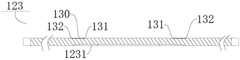
环形走线区130,内环边缘131,外环边缘132,Ring-
银边区141。Silver Edge 141.
具体实施方式Detailed ways
下面详细描述本申请的实施例,所述实施例的示例在附图中示出,其中自始至终相同或类似的标号表示相同或类似的元件或具有相同或类似功能的元件。下面通过参考附图描述的实施例是示例性的,仅用于解释本申请,而不能理解为对本申请的限制。The following describes in detail the embodiments of the present application, examples of which are illustrated in the accompanying drawings, wherein the same or similar reference numerals refer to the same or similar elements or elements having the same or similar functions throughout. The embodiments described below with reference to the accompanying drawings are exemplary and are only used to explain the present application, but should not be construed as a limitation on the present application.
下面参考图1-图9描述根据本申请实施例的电子设备的屏幕组件102及电子设备100。The
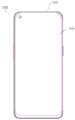
如图1所示,根据本申请实施例的电子设备的屏幕组件102,包括摄像头110和显示组件120。As shown in FIG. 1 , a
具体而言,如图8所示,显示组件120可以包括从上至下依次层叠设置的盖板121、光学胶层1211、偏光片122、上玻璃123、下玻璃124以及泡棉层125。其中,如图4所示,光学胶层1211可以用于将盖板121和偏光片122粘接在一起,也即盖板121与偏光片122粘接,而盖板121与偏光片122之间的粘接结构可以为光学胶层1211。光学胶层1211可以由具有透光效果的胶水固化形成。偏光片122具有第一通光孔1221,泡棉层125具有第二通光孔1251,第一通光孔1221和第二通光孔1251相对。如图8、图9所示,摄像头110设于显示组件120下方。进一步地,摄像头110的进光端111位于显示组件120下方。Specifically, as shown in FIG. 8 , the display assembly 120 may include a
摄像头110在拍摄照片时,光线可以通过第一通光孔1221、第二通光孔1251进入到摄像头110的进光端111,摄像头110可以根据光线的信息进行成像。如图8所示,摄像头110的光轴与第一通光孔1221的轴线、第二通光孔1251的轴线平行。优选地,摄像头110的光轴与第一通光孔1221的轴线、第二通光孔1251的轴线共线。需要说明的是,通过将摄像头110设置在显示组件120下方,可以无需在屏幕组件102预留放置摄像头110的区域(例如可以取消屏幕组件102上用于放置摄像头110的水滴结构或小刘海结构),由此可以使屏幕组件102具有全面屏结构,即实现具有屏下摄像头110的全面屏结构。When the
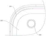
需要说明的是,显示组件120可以为OLED显示屏。OLED显示屏可以包括盖板121、光学胶层1211、偏光片122、上玻璃123、下玻璃124以及泡棉层125。这里的盖板121可以为玻璃盖板,可以用于保护盖板121下方的部件。OLED显示屏内部具有走线区域,该走线区域内的金属线,可以为OLED显示屏供电,以使其具有显示功能。为了方便设置摄像头110,可以将该走线区域设置成环形结构,也即OLED显示屏的走线区域可以包括环形走线区130。此外,还需要说明的是,显示组件120上与摄像头110对应且不显示图像的区域103,环形走线区130为不透光区域,环形走线区130域可以环绕在区域103的外周。It should be noted that the display assembly 120 may be an OLED display screen. The OLED display screen may include a
如图2所示,显示组件上与摄像头对应且不显示图像的区域103,可以为圆形。当然这里对显示组件上与摄像头对应且不显示图像的区域103的形状不做具体限定,例如,如图3所示,显示组件上与摄像头对应且不显示图像的区域103可以为长圆形。As shown in FIG. 2 , the
如图6、图8以及图9所示,环形走线区130设于上玻璃123的上表面,环形走线区130包括内环边缘131和外环边缘132,第一通光孔1221的内壁位于内环边缘131的径向外侧,光线适于从盖板121、光学胶层1211、第一通光孔1221、内环边缘131限定出的环内区域、上玻璃123、下玻璃124以及第二通光孔1251传递至摄像头110。As shown in FIG. 6 , FIG. 8 and FIG. 9 , the
根据本申请实施例的电子设备的屏幕组件102,通过将第一通光孔1221的内壁设于环形走线区130的内环边缘131的径向外侧,可以利用第一通光孔1221和第二通光孔1251的结构,显示组件120与摄像头110相对的位置处形成盲孔结构,第一通光孔1221的内壁位于内环边缘131的径向外侧,可以使换向走线区的部分结构露出,以形成银边区141,银边区141的设计可以利用视觉差异,使显示组件120上与摄像头110对应且不显示图像的区域103变小,从而可以改善屏幕组件102的显示效果。According to the
为了进一步改善屏幕组件102的显示效果,如图9所示,在环形走线区130域的径向方向上,第一通光孔1221的内壁位于内环边缘131之间的距离为L1,L1的取值范围为0.15-0.25mm。经验证,当L1=0.2mm时,从视觉上看,显示组件120上与摄像头110对应且不显示图像的区域103更小,屏幕组件102的显示效果更好。更进一步地,第一通光孔1221的内壁位于外环边缘132的径向内侧。也就是说,第一通光孔1221的内壁位于外环边缘132和内环边缘131之间。In order to further improve the display effect of the
如图8、图9所示,摄像头110与显示组件120的视场角可以为α,其中α为79°-82°。需要说明的是,视场角可以与环形走线区130的宽度、第一通光孔1221的深度、第二通光孔1251的深度相关,通过限定视场角的数值范围,可以优化环形走线区130的宽度、第一通光孔1221的深度、第二通光孔1251的深度等参数数值,进而可以优化屏幕组件102的结构。经过验证,当α=80.4°时,屏幕组件102的结构更优。As shown in FIGS. 8 and 9 , the angle of view between the
如图8、图9所示,在环形走线区130域的径向方向上,内环边缘131与外环边缘132之间的距离为L2,L2为0.4-0.5mm。也就是说,环形走线区130的宽度可以为0.4-0.5mm。经验证,当L2=0.45mm时,环形走线区130不但可以满足屏幕组件102的使用需求,还可减小环形走线区130的宽度,进而可以减小显示组件120上与摄像头110对应且不显示图像的区域103的面积,进而可以提升屏幕组件102的显示效果。为了进一步地增加上玻璃123的透光度,优化摄像头110成像效果,如图6、图9所示,上玻璃123的下表面具有凹槽1231,凹槽1231与所述第二通光孔1251相对。As shown in FIGS. 8 and 9 , in the radial direction of the
如图9所示,摄像头110的上表面位于第二通光孔1251内,由此可以在上下方向上降低摄像头110与显示组件120之间的高度。进一步地,如图9所示,摄像头110的上表面与所述下玻璃124的下表面距离为L3,所述L3为0.1-0.3mm。经验证,当L3=0.15mm时,屏幕组件102的结构紧凑度更好,摄像头110的成像效果更优。As shown in FIG. 9 , the upper surface of the
如图1-图9所示,根据本申请实施例的电子设备100,包括壳体101、摄像头110、显示组件120和环形走线区130。显示组件120嵌设于壳体101,显示组件120包括从上至下依次层叠设置的盖板121、光学胶层1211、偏光片122、上玻璃123、下玻璃124以及泡棉层125,偏光片122具有第一通光孔1221,泡棉层125具有第二通光孔1251,第一通光孔1221和第二通光孔1251相对,摄像头110设于壳体101内且位于显示组件120下方。如图8、图9所示,摄像头110设于显示组件120下方。进一步地,摄像头110的进光端111位于显示组件120下方。As shown in FIGS. 1-9 , an
摄像头110在拍摄照片时,光线可以通过第一通光孔1221、第二通光孔1251进入到摄像头110的进光端111,摄像头110可以根据光线的信息进行成像。如图8所示,摄像头110的光轴与第一通光孔1221的轴线、第二通光孔1251的轴线平行。摄像头110的光轴与第一通光孔1221的轴线、第二通光孔1251的轴线共线。需要说明的是,通过将摄像头110设置在显示组件120下方,可以无需在屏幕组件102预留放置摄像头110的区域(例如可以取消屏幕组件102上用于放置摄像头110的水滴结构或小刘海结构),由此可以使屏幕组件102具有全面屏结构,即可以实现具有屏下摄像头110的全面屏结构。When the
需要说明的是,显示组件120可以为OLED显示屏。OLED显示屏可以包括盖板121、光学胶层1211、偏光片122、上玻璃123、下玻璃124以及泡棉层125。OLED显示屏内部具有走线区域,该走线区域内的金属线,可以为OLED显示屏供电,以使其具有显示功能。为了方便设置摄像头110,可以将该走线区域设置成环形结构,也即OLED显示屏的走线区域可以包括环形走线区130。此外,还需要说明的是,显示组件120上与摄像头110对应且不显示图像的区域103,环形走线区130为不透光区域,环形走线区130域可以环绕在区域103的外周。It should be noted that the display assembly 120 may be an OLED display screen. The OLED display screen may include a
如图6、图8以及图9所示,环形走线区130设于所述上玻璃123的上表面,环形走线区130包括内环边缘131和外环边缘132,第一通光孔1221的内壁位于所述内环边缘131的径向外侧,光线适于从盖板121、光学胶层1211、所述第一通光孔1221、所述内环边缘131限定出的环内区域、所述上玻璃123、所述下玻璃124以及所述第二通光孔1251传递至所述摄像头110。As shown in FIG. 6 , FIG. 8 and FIG. 9 , the
如图7、图8所示,摄像头110可以通过支架112安装在壳体101内,摄像头110可以通过柔性电路板114,以及设置在柔性电路板114上的连接座113与电子设备100的主板104电连接,从而可以将摄像头110采集到的光线信息传递到主板104。As shown in FIG. 7 and FIG. 8 , the
根据本申请实施例的电子设备100,通过将第一通光孔1221的内壁设于环形走线区130的内环边缘131的径向外侧,可以利用第一通光孔1221和第二通光孔1251的结构,显示组件120与摄像头110相对的位置处形成盲孔结构,第一通光孔1221的内壁位于内环边缘131的径向外侧,可以使换向走线区的部分结构露出,以形成银边区141,银边区141的设计可以利用视觉差异,使显示组件120上与摄像头110对应且不显示图像的区域103变小,从而可以改善屏幕组件102的显示效果。According to the
在本申请的描述中,需要理解的是,术语“中心”、“长度”、“上”、“下”、“水平”、“内”、“外”、“轴向”、“径向”、“周向”等指示的方位或位置关系为基于附图所示的方位或位置关系,仅是为了便于描述本申请和简化描述,而不是指示或暗示所指的装置或元件必须具有特定的方位、以特定的方位构造和操作,因此不能理解为对本申请的限制。在本申请的描述中,“多个”的含义是两个或两个以上。In the description of this application, it is to be understood that the terms "central", "length", "upper", "lower", "horizontal", "inner", "outer", "axial", "radial" The orientation or positional relationship indicated by , "circumferential direction", etc. is based on the orientation or positional relationship shown in the accompanying drawings, which is only for the convenience of describing the present application and simplifying the description, rather than indicating or implying that the indicated device or element must have a specific Orientation, construction and operation in a particular orientation, and therefore should not be construed as a limitation of the present application. In the description of this application, "plurality" means two or more.
在本说明书的描述中,参考术语“一个实施例”、“一些实施例”、“示意性实施例”、“示例”、“具体示例”、或“一些示例”等的描述意指结合该实施例或示例描述的具体特征、结构、材料或者特点包含于本申请的至少一个实施例或示例中。在本说明书中,对上述术语的示意性表述不一定指的是相同的实施例或示例。而且,描述的具体特征、结构、材料或者特点可以在任何的一个或多个实施例或示例中以合适的方式结合。In the description of this specification, reference to the terms "one embodiment," "some embodiments," "exemplary embodiment," "example," "specific example," or "some examples", etc., is meant to incorporate the embodiments A particular feature, structure, material, or characteristic described by an example or example is included in at least one embodiment or example of the present application. In this specification, schematic representations of the above terms do not necessarily refer to the same embodiment or example. Furthermore, the particular features, structures, materials or characteristics described may be combined in any suitable manner in any one or more embodiments or examples.
尽管已经示出和描述了本申请的实施例,本领域的普通技术人员可以理解:在不脱离本申请的原理和宗旨的情况下可以对这些实施例进行多种变化、修改、替换和变型,本申请的范围由权利要求及其等同物限定。Although the embodiments of the present application have been shown and described, it will be understood by those of ordinary skill in the art that various changes, modifications, substitutions and alterations can be made in these embodiments without departing from the principles and spirit of the present application, The scope of the application is defined by the claims and their equivalents.
Claims (13)
Priority Applications (4)
| Application Number | Priority Date | Filing Date | Title |
|---|---|---|---|
| CN201910983586.0ACN110769095B (en) | 2019-10-16 | 2019-10-16 | Screen assembly of electronic equipment and electronic equipment |
| EP20876802.8AEP4024831A4 (en) | 2019-10-16 | 2020-09-22 | Screen assembly of electronic device, and electronic device |
| PCT/CN2020/116890WO2021073374A1 (en) | 2019-10-16 | 2020-09-22 | Screen assembly of electronic device, and electronic device |
| US17/691,773US20220197339A1 (en) | 2019-10-16 | 2022-03-10 | Screen assembly of electronic device, and electronic device |
Applications Claiming Priority (1)
| Application Number | Priority Date | Filing Date | Title |
|---|---|---|---|
| CN201910983586.0ACN110769095B (en) | 2019-10-16 | 2019-10-16 | Screen assembly of electronic equipment and electronic equipment |
Publications (2)
| Publication Number | Publication Date |
|---|---|
| CN110769095Atrue CN110769095A (en) | 2020-02-07 |
| CN110769095B CN110769095B (en) | 2022-05-20 |
Family
ID=69332494
Family Applications (1)
| Application Number | Title | Priority Date | Filing Date |
|---|---|---|---|
| CN201910983586.0AActiveCN110769095B (en) | 2019-10-16 | 2019-10-16 | Screen assembly of electronic equipment and electronic equipment |
Country Status (4)
| Country | Link |
|---|---|
| US (1) | US20220197339A1 (en) |
| EP (1) | EP4024831A4 (en) |
| CN (1) | CN110769095B (en) |
| WO (1) | WO2021073374A1 (en) |
Cited By (2)
| Publication number | Priority date | Publication date | Assignee | Title |
|---|---|---|---|---|
| WO2021073374A1 (en)* | 2019-10-16 | 2021-04-22 | Oppo广东移动通信有限公司 | Screen assembly of electronic device, and electronic device |
| EP4131918A4 (en)* | 2020-03-30 | 2023-09-20 | Vivo Mobile Communication Co., Ltd. | Electronic device |
Families Citing this family (2)
| Publication number | Priority date | Publication date | Assignee | Title |
|---|---|---|---|---|
| CN110867136B (en)* | 2019-11-22 | 2021-10-15 | 维沃移动通信有限公司 | Pole screen and electronic equipment |
| CN119094876B (en)* | 2024-08-08 | 2025-04-04 | 华为技术有限公司 | Motor assembly, assembling method thereof, camera module and electronic equipment |
Citations (4)
| Publication number | Priority date | Publication date | Assignee | Title |
|---|---|---|---|---|
| US20170235398A1 (en)* | 2016-02-16 | 2017-08-17 | Samsung Electronics Co., Ltd. | Electronic device |
| CN107395928A (en)* | 2017-08-01 | 2017-11-24 | 维沃移动通信有限公司 | A kind of optical module and mobile terminal |
| CN208862900U (en)* | 2018-09-28 | 2019-05-14 | 维沃移动通信有限公司 | A display panel and terminal equipment |
| CN209388081U (en)* | 2019-03-27 | 2019-09-13 | 信利光电股份有限公司 | A kind of display device |
Family Cites Families (4)
| Publication number | Priority date | Publication date | Assignee | Title |
|---|---|---|---|---|
| CN108989508B (en)* | 2018-08-24 | 2021-03-26 | Oppo(重庆)智能科技有限公司 | Display screen assembling method, display screen and electronic equipment |
| CN208672989U (en)* | 2018-09-29 | 2019-03-29 | Oppo广东移动通信有限公司 | Display screen assembly and electronic device having the same |
| CN110769095B (en)* | 2019-10-16 | 2022-05-20 | Oppo广东移动通信有限公司 | Screen assembly of electronic equipment and electronic equipment |
| CN110728905B (en)* | 2019-11-18 | 2021-01-26 | 维沃移动通信有限公司 | Electronic device |
- 2019
- 2019-10-16CNCN201910983586.0Apatent/CN110769095B/enactiveActive
- 2020
- 2020-09-22WOPCT/CN2020/116890patent/WO2021073374A1/ennot_activeCeased
- 2020-09-22EPEP20876802.8Apatent/EP4024831A4/ennot_activeWithdrawn
- 2022
- 2022-03-10USUS17/691,773patent/US20220197339A1/ennot_activeAbandoned
Patent Citations (4)
| Publication number | Priority date | Publication date | Assignee | Title |
|---|---|---|---|---|
| US20170235398A1 (en)* | 2016-02-16 | 2017-08-17 | Samsung Electronics Co., Ltd. | Electronic device |
| CN107395928A (en)* | 2017-08-01 | 2017-11-24 | 维沃移动通信有限公司 | A kind of optical module and mobile terminal |
| CN208862900U (en)* | 2018-09-28 | 2019-05-14 | 维沃移动通信有限公司 | A display panel and terminal equipment |
| CN209388081U (en)* | 2019-03-27 | 2019-09-13 | 信利光电股份有限公司 | A kind of display device |
Cited By (2)
| Publication number | Priority date | Publication date | Assignee | Title |
|---|---|---|---|---|
| WO2021073374A1 (en)* | 2019-10-16 | 2021-04-22 | Oppo广东移动通信有限公司 | Screen assembly of electronic device, and electronic device |
| EP4131918A4 (en)* | 2020-03-30 | 2023-09-20 | Vivo Mobile Communication Co., Ltd. | Electronic device |
Also Published As
| Publication number | Publication date |
|---|---|
| US20220197339A1 (en) | 2022-06-23 |
| WO2021073374A1 (en) | 2021-04-22 |
| CN110769095B (en) | 2022-05-20 |
| EP4024831A1 (en) | 2022-07-06 |
| EP4024831A4 (en) | 2022-11-23 |
Similar Documents
| Publication | Publication Date | Title |
|---|---|---|
| CN110769095B (en) | Screen assembly of electronic equipment and electronic equipment | |
| CN106843398B (en) | electronic device | |
| CN107229148B (en) | Display screen, display device and mobile terminal | |
| CN206674022U (en) | Input and output modules and electronic devices | |
| CN108897174A (en) | screen assembly and electronic device | |
| CN113760050B (en) | Screen assembly of electronic equipment and electronic equipment | |
| CN104506760A (en) | Camera sealing structure and terminal | |
| CN108391038B (en) | Electronic device and camera assembly thereof | |
| CN113421900A (en) | Display module, manufacturing method of display module and display device | |
| CN110646962A (en) | Display assembly, electronic device, and manufacturing method of electronic device | |
| CN113746958A (en) | Electronic device and method for assembling electronic device | |
| WO2022127660A1 (en) | Camera module and electronic device | |
| CN112135013B (en) | Electronic equipment | |
| CN112736111A (en) | Screen module and electronic equipment | |
| CN114694483A (en) | Display module and display device | |
| CN110740201B (en) | Screen assembly of electronic equipment and electronic equipment | |
| CN113840056B (en) | Camera module and electronic equipment | |
| CN108052168A (en) | Assemble method, display screen component and the electronic equipment of display screen component | |
| CN209845079U (en) | Camera module connection structure, screen and terminal applied to in-plane hole-digging screen | |
| JPWO2017163560A1 (en) | Housing mounting member and electronic device | |
| CN209517201U (en) | A kind of mobile terminal | |
| WO2022127658A1 (en) | Photographic module, and electronic device | |
| CN207851683U (en) | Display components and electronic equipment | |
| CN112969010A (en) | Electronic device | |
| CN206332722U (en) | Circuit board arrangement and mobile terminal |
Legal Events
| Date | Code | Title | Description |
|---|---|---|---|
| PB01 | Publication | ||
| PB01 | Publication | ||
| SE01 | Entry into force of request for substantive examination | ||
| SE01 | Entry into force of request for substantive examination | ||
| GR01 | Patent grant | ||
| GR01 | Patent grant |