CN110768020A - Frequency selective surface structure - Google Patents
Frequency selective surface structureDownload PDFInfo
- Publication number
- CN110768020A CN110768020ACN201810832697.7ACN201810832697ACN110768020ACN 110768020 ACN110768020 ACN 110768020ACN 201810832697 ACN201810832697 ACN 201810832697ACN 110768020 ACN110768020 ACN 110768020A
- Authority
- CN
- China
- Prior art keywords
- frequency selective
- selective surface
- surface structure
- layer
- groove
- Prior art date
- Legal status (The legal status is an assumption and is not a legal conclusion. Google has not performed a legal analysis and makes no representation as to the accuracy of the status listed.)
- Pending
Links
- 239000002184metalSubstances0.000claimsdescription21
- 229910052751metalInorganic materials0.000claimsdescription21
- 150000002894organic compoundsChemical class0.000claimsdescription6
- OKTJSMMVPCPJKN-UHFFFAOYSA-NCarbonChemical compound[C]OKTJSMMVPCPJKN-UHFFFAOYSA-N0.000claimsdescription4
- 229910021389grapheneInorganic materials0.000claimsdescription4
- 239000010410layerSubstances0.000description50
- RYGMFSIKBFXOCR-UHFFFAOYSA-NCopperChemical compound[Cu]RYGMFSIKBFXOCR-UHFFFAOYSA-N0.000description13
- 229910052802copperInorganic materials0.000description11
- 239000010949copperSubstances0.000description11
- 238000000034methodMethods0.000description9
- 239000000463materialSubstances0.000description6
- 238000002834transmittanceMethods0.000description6
- 230000008569processEffects0.000description5
- 238000011160researchMethods0.000description5
- 230000005540biological transmissionEffects0.000description4
- 238000010586diagramMethods0.000description4
- 230000000737periodic effectEffects0.000description3
- 230000000694effectsEffects0.000description2
- 229920005570flexible polymerPolymers0.000description2
- 230000003993interactionEffects0.000description2
- -1polyethylene terephthalatePolymers0.000description2
- 229920000139polyethylene terephthalatePolymers0.000description2
- 239000005020polyethylene terephthalateSubstances0.000description2
- 229920000642polymerPolymers0.000description2
- 229920000193polymethacrylatePolymers0.000description2
- 230000004044responseEffects0.000description2
- 230000001629suppressionEffects0.000description2
- 238000004458analytical methodMethods0.000description1
- 238000004891communicationMethods0.000description1
- 238000013461designMethods0.000description1
- 238000001514detection methodMethods0.000description1
- 238000011161developmentMethods0.000description1
- 230000005672electromagnetic fieldEffects0.000description1
- 238000004049embossingMethods0.000description1
- 238000005516engineering processMethods0.000description1
- 230000002708enhancing effectEffects0.000description1
- 230000003628erosive effectEffects0.000description1
- 238000001914filtrationMethods0.000description1
- 238000003475laminationMethods0.000description1
- 238000004519manufacturing processMethods0.000description1
- 230000013011matingEffects0.000description1
- 230000003287optical effectEffects0.000description1
- 230000005693optoelectronicsEffects0.000description1
- 230000035699permeabilityEffects0.000description1
- 230000010287polarizationEffects0.000description1
- 239000011241protective layerSubstances0.000description1
- 230000009897systematic effectEffects0.000description1
- 230000009466transformationEffects0.000description1
Images


Classifications
- H—ELECTRICITY
- H01—ELECTRIC ELEMENTS
- H01Q—ANTENNAS, i.e. RADIO AERIALS
- H01Q15/00—Devices for reflection, refraction, diffraction or polarisation of waves radiated from an antenna, e.g. quasi-optical devices
- H01Q15/0006—Devices acting selectively as reflecting surface, as diffracting or as refracting device, e.g. frequency filtering or angular spatial filtering devices
- H01Q15/0013—Devices acting selectively as reflecting surface, as diffracting or as refracting device, e.g. frequency filtering or angular spatial filtering devices said selective devices working as frequency-selective reflecting surfaces, e.g. FSS, dichroic plates, surfaces being partly transmissive and reflective
- G—PHYSICS
- G02—OPTICS
- G02B—OPTICAL ELEMENTS, SYSTEMS OR APPARATUS
- G02B5/00—Optical elements other than lenses
Landscapes
- Physics & Mathematics (AREA)
- General Physics & Mathematics (AREA)
- Optics & Photonics (AREA)
- Aerials With Secondary Devices (AREA)
Abstract
Translated fromChinese
Description
Translated fromChinese技术领域technical field
本发明涉及电磁场与微波技术领域,尤其涉及一种频率选择表面结构。The invention relates to the technical field of electromagnetic fields and microwaves, in particular to a frequency selective surface structure.
背景技术Background technique
频率选择表面结构(Frequency Selective Surface,FSS)广泛应用于微波段和红外波段的频率选择表面结构,可用作滤波器,雷达罩,反射天线,隐身材料等,早在上世纪六十年代,国外就开展了频率选择表面结构(Frequency Selective Surface,FSS)的研究,目前已有较为系统的研究理论。国内在有关FSS的研究较晚,由于FSS广阔的应用领域,尤其是卫星通信和雷达系统,以及潜在的商业价值,近些年来发展十分迅速。FSS的理论与应用己成为微波毫米波技术领域的一个发展方向。但是到目前为止,我国对FSS的分析研究仍然与国外存在较大的差距,仅仅限于几种特殊的结构单元,鲜有对于特殊形状结构或者多层导电层频率选择表面结构的电磁响应特性研究。Frequency Selective Surface (FSS) is widely used in frequency selective surface structures in microwave and infrared bands, and can be used as filters, radomes, reflective antennas, stealth materials, etc. As early as the 1960s, foreign The research on frequency selective surface structure (Frequency Selective Surface, FSS) has been carried out, and there is a relatively systematic research theory at present. Domestic research on FSS is relatively late. Due to the broad application fields of FSS, especially satellite communication and radar systems, as well as potential commercial value, it has developed rapidly in recent years. The theory and application of FSS has become a development direction in the field of microwave and millimeter wave technology. However, so far, the analysis and research of FSS in my country is still far behind that of foreign countries. It is limited to a few special structural units, and there is little research on the electromagnetic response characteristics of special shape structures or frequency selective surface structures of multilayer conductive layers.
频率选择表面结构(Frequency Selective Surface,FSS)是由大量无源谐振单元组成的单屏或多屏周期性阵列结构,由周期性排列的金属贴片单元或在金属屏上周期性排列的孔径单元构成。其频率选择性源于其周期性结构与电磁波的相互作用,是一个对电磁波的入射角、极化方式、频率均有选择作用的空间滤波器。这种表面可以在单元谐振频率附近呈现全反射(贴片型金属结构单元)或全透射(孔径型金属结构单元)。FSS与电磁波相互作用表现出明显的带阻(贴片型金属结构单元)或带通(孔径型金属结构单元)的滤波特性。FSS能对电磁波起到频率过滤的作用。它对电磁波的响应特性随着频率而变化,相同单元结构的FSS的中心工作频率和带宽受金属磁导率的影响而变化。带阻型FSS在中心频带内的入射电磁波呈现反射特性,而其他频带的入射电磁波则呈现透射特性。Frequency Selective Surface (FSS) is a single-screen or multi-screen periodic array structure composed of a large number of passive resonant units, which consists of periodically arranged metal patch units or periodically arranged aperture units on the metal screen. constitute. Its frequency selectivity originates from the interaction between its periodic structure and electromagnetic waves. It is a spatial filter that can select the incident angle, polarization mode and frequency of electromagnetic waves. Such surfaces can exhibit either total reflection (patch-type metal structure elements) or total transmission (aperture-type metal structure elements) around the element resonance frequency. The interaction of FSS with electromagnetic waves exhibits obvious band-stop (patch-type metal structural elements) or band-pass (aperture-type metal structural elements) filtering characteristics. FSS can filter the frequency of electromagnetic waves. Its response characteristics to electromagnetic waves vary with frequency, and the central operating frequency and bandwidth of the FSS with the same unit structure are affected by the magnetic permeability of the metal. In the band-stop FSS, the incident electromagnetic wave in the central frequency band exhibits reflection characteristics, while the incident electromagnetic waves in other frequency bands exhibit transmission characteristics.
但是,贴片型金属结构单元由于采用将金属结构单元凸出的贴合在支撑层外表面上,因此相对于内嵌型其厚度较厚,使FSS柔性差,整体透光率不高,三维曲面化难度大,设计难度大,制作工艺复杂的技术难题。However, the patch-type metal structural unit uses the protruding metal structural unit to stick to the outer surface of the support layer, so the thickness is thicker than the embedded type, which makes the FSS less flexible, the overall light transmittance is not high, and the three-dimensional The surface is difficult, the design is difficult, and the production process is complicated.
发明内容SUMMARY OF THE INVENTION
本发明的目的主要在于提供一种易于三维曲面化的频率选择表面结构。The main purpose of the present invention is to provide a frequency selective surface structure which is easy to be three-dimensionally curved.
为实现前述发明目的,本发明提供一种频率选择表面结构,包括支撑层和导电层,所述支撑层的一侧表面设有图形凹槽,所述凹槽为镂空网状结构,所述导电层设于所述图形凹槽内。In order to achieve the aforementioned purpose of the invention, the present invention provides a frequency selective surface structure, which includes a support layer and a conductive layer. One side surface of the support layer is provided with a pattern groove, and the groove is a hollow mesh structure. The layer is arranged in the pattern groove.
在其中一实施例中,所述导电层包括至少一个导电单元。In one embodiment, the conductive layer includes at least one conductive unit.
在其中一实施例中,所述导电单元材质为金属或石墨烯。In one embodiment, the material of the conductive unit is metal or graphene.
在其中一实施例中,所述图形凹槽包括至少一个凹槽单元。In one embodiment, the pattern groove includes at least one groove unit.
在其中一实施例中,多个所述凹槽单元呈周期性排布或非周期性排布。In one embodiment, a plurality of the groove units are arranged periodically or aperiodically.
在其中一实施例中,多个所述凹槽单元之间没有间隔,或至少一个方向上有间隔。In one embodiment, there is no space between a plurality of the groove units, or there is space in at least one direction.
在其中一实施例中,所述凹槽单元为镂空“十”字型网状结构。In one embodiment, the groove unit is a hollow "cross"-shaped mesh structure.
在其中一实施例中,所述支撑层由柔性高分子有机化合物制成。In one embodiment, the support layer is made of a flexible polymer organic compound.
在其中一实施例中,所述频率选择表面结构还包括覆盖层,所述覆盖层至少部分覆盖所述导电层或/和所述覆盖层至少部分覆盖所述支撑层。In one of the embodiments, the frequency selective surface structure further comprises a cover layer, the cover layer at least partially covers the conductive layer or/and the cover layer at least partially covers the support layer.
在其中一实施例中,所述覆盖层由柔性高分子有机化合物制成。In one embodiment, the cover layer is made of a flexible polymer organic compound.
本发明实施例在于提供一种频率选择表面结构,通过将导电层嵌入支撑层表面的镂空网状机构的图形凹槽中形成导电层单元层,使整体频率选择表面结构的厚度可设计得较小,减少了材料的使用,增加了透光率,实现超薄的频率选择表面结构,解决了频率选择表面结构三维曲面化困难的技术难题。The embodiment of the present invention is to provide a frequency selective surface structure. By embedding the conductive layer in the pattern groove of the hollow mesh structure on the surface of the support layer to form a conductive layer unit layer, the thickness of the overall frequency selective surface structure can be designed to be smaller. , reducing the use of materials, increasing the light transmittance, realizing an ultra-thin frequency selective surface structure, and solving the technical problem that the frequency selective surface structure is difficult to three-dimensionally curved.
附图说明Description of drawings
图1为本发明实施例支撑层结构示意图;1 is a schematic diagram of a support layer structure according to an embodiment of the present invention;
图2为本发明实施例支撑层和导电层结构示意图;2 is a schematic structural diagram of a support layer and a conductive layer according to an embodiment of the present invention;
图3为本发明实施例频率选择表面结构示意图;3 is a schematic diagram of a frequency selective surface structure according to an embodiment of the present invention;
图4为本发明实施例毫米级金属结构单元的频率选择表面结构带阻频段在微波区域的透波特性曲线;Fig. 4 is the wave transmission characteristic curve of the band-stop frequency band of the frequency selective surface structure of the millimeter-scale metal structural unit in the microwave region according to the embodiment of the present invention;
图5为本发明实施例微米级金属结构单元的频率选择表面结构带阻频段在红外波区域的透波特性曲线;Fig. 5 is the wave transmittance characteristic curve of the band-stop frequency band of the frequency selective surface structure of the micron-scale metal structural unit in the infrared wave region according to the embodiment of the present invention;
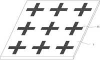
图6为本发明实施例频率选择表面的布局图。FIG. 6 is a layout diagram of a frequency selection surface according to an embodiment of the present invention.
具体实施方式Detailed ways
为更进一步阐述本发明为达成预定发明目的所采取的技术方案及功效,以下结合附图及实施例,对本发明的具体实施方式、结构、特征及其功效,详细说明如后。In order to further illustrate the technical solutions and effects adopted by the present invention to achieve the predetermined purpose of the invention, the specific embodiments, structures, features and effects of the present invention are described in detail below with reference to the accompanying drawings and examples.
请参考图1-图3,本发明实施例公开一种频率选择表面结构,包括支撑层1和导电层2,支撑层1的一侧表面上设有图形凹槽11,该图像凹槽为镂空网状结构,导电层设于图形凹槽11。Please refer to FIG. 1 to FIG. 3 , an embodiment of the present invention discloses a frequency selective surface structure, including a
在本实施例中,该频率选择表面结构为带阻型频率选择表面结构。In this embodiment, the frequency selective surface structure is a band-stop frequency selective surface structure.
支撑层2采用柔性透明的高分子有机化合物(例如,聚甲基丙烯酸酯或聚对苯二甲酸乙二醇酯)制成,具有较好的柔性和透光率,可贴合在任意曲面上。The
图形凹槽包括至少一个凹槽单元11,在同一频率选择表面结构中,多个凹槽单元11之间无间隔或至少一个方向上有间隔;多个凹槽单元11呈周期性排布或非周期性排布,优选地,采用阵列或蜂窝状排列。在本实施例中,凹槽单元11呈镂空“十”字型网状结构,采用压印的方式在支撑层1上制作。凹槽单元11的数量根据需要决定,如支撑层1的大小或阻带的频率,可为一个或多个,同时,凹槽单元11的图形形状也根据不同的阻带频率设计。The pattern groove includes at least one
导电层2包括至少一个导电单元,导电单元为金属结构单元。一个或多个金属结构单元组成金属结构单元层2,具体地,金属结构单元可为铜结构单元。金属结构单元由熔融的金属通过填充的方式嵌入凹槽单元11内形成,金属结构单元表面与支撑层1表面齐平。因此,金属结构单元的图形与凹槽单元11对应。The
镂空十字型等形状图案的导电层2具有较低的占空比,减少的材料的使用,提高了透光率,与此同时,极薄的导电层2自身也带有一定柔性。制作的频率选择表面结构具备优良的柔性,从而令频率选择表面结构在贴合过程中不受贴合体外形的影响,这种结构的频率选择表面结构在具备光学高透过率的同时,又不影响贴合面的正常视图,可用作特定的观测和探测功能的高透明性光学窗,方法简单、易行。The
不同频段的带阻型频率选择表面结构的频率选择特性由导电单元的特性(导电单元的图形、线宽、厚度,材质)来实现。在本实施例中,导电单元层呈矩形阵列排布,且以铜材质制作导电单元。如图2、图4和图6,当支撑层1厚度为0.1mm,铜结构单元(镂空“十”字型网状结构)十字宽度S1为0.44mm,十字线长S2为3mm,十字的网格线的线宽S6为0.04mm,厚度为0.05mm,网格线之间的间距S5为0.1mm,纵向相邻的铜结构单元的间隔S4为0.2mm,横向相邻的铜结构单元的间隔S3为0.2mm时,此时铜结构单元为毫米级,毫米级铜结构单元的频率选择表面结构的带阻频段处于微波区域,在通道边缘的透射率出现陡降,传输系数迅速下降到-53dB,并在此后较宽的频带(43.8GHz-46.6GHz)内保持在-20dB以下,带外抑制性能良好。如图2、图5和图6,当支撑层1厚度为30um,铜结构单元(镂空“十”字型网状结构)十字宽度S1为44um,十字线长S2为300um,十字的网格线的线宽S6为4um,厚度为15um,网格线之间的间距S5为10um,纵向相邻的铜结构单元的间隔S4为20um,横向相邻的铜结构单元的间隔S3为20um时,此时铜结构单元为微米级铜结构单元的频率选择表面结构的带阻频段在红外波区域,在通道边缘透射率出现陡降,反射率出现陡增的特性,传输系数迅速下降到-47dB,并在此后较宽的频带(420GHz-455GHz)内保持在-20dB以下,带外抑制性能良好。由上述可知,随着铜结构单元尺寸的增大,阻带由红外波段向微波段偏移。The frequency selective properties of the band-stop frequency selective surface structures in different frequency bands are realized by the properties of the conductive elements (pattern, line width, thickness, and material of the conductive elements). In this embodiment, the conductive unit layers are arranged in a rectangular array, and the conductive units are made of copper material. As shown in Figure 2, Figure 4 and Figure 6, when the thickness of the
在其他实施例中,导电层2也可由将石墨烯嵌入图形凹槽中形成,石墨烯透明度高,且质地薄,其优异的电光效应使得所述频率选择表面结构具备高透明度和较好的柔韧性。In other embodiments, the
导电层2上设有覆盖层3,覆盖层3可通过贴合的方式至少部分覆盖导电层2或/和覆盖层3至少部分覆盖支撑层1。在本实施例中,覆盖层3采用柔性透明的高分子有机化合物制成(例如聚甲基丙烯酸酯或聚对苯二甲酸乙二醇酯),覆盖层3作为导电层2的防护层覆盖整个频率选择表面结构的表面,保护导电层2不受外界环境的侵蚀,从而增加了频率选择表面结构的使用寿命以及稳定性,同时使导电层2与支撑层1的贴合更紧密,增强了导电层2与支撑结构之间的附着力。The
需要说明的是,在本文中,术语“包括”、“包含”或者其任何其他变体意在涵盖非排他性的包含,从而使得包括一系列要素的过程、方法、物品或者装置不仅包括那些要素,而且还包括没有明确列出的其他要素,或者是还包括为这种过程、方法、物品或者装置所固有的要素。在没有更多限制的情况下,由语句“包括一个……”限定的要素,并不排除在包括该要素的过程、方法、物品或者装置中还存在另外的相同要素。It should be noted that, herein, the terms "comprising", "comprising" or any other variation thereof are intended to encompass non-exclusive inclusion, such that a process, method, article or device comprising a series of elements includes not only those elements, It also includes other elements not expressly listed or inherent to such a process, method, article or apparatus. Without further limitation, an element qualified by the phrase "comprising a..." does not preclude the presence of additional identical elements in a process, method, article or apparatus that includes the element.
以上仅为本发明的优选实施例,并非因此限制本发明的专利范围,凡是利用本发明说明书及附图内容所作的等效结构或等效流程变换,或直接或间接运用在其他相关的技术领域,均同理包括在本发明的专利保护范围内。The above are only preferred embodiments of the present invention, and are not intended to limit the scope of the present invention. Any equivalent structure or equivalent process transformation made by using the contents of the description and drawings of the present invention, or directly or indirectly applied in other related technical fields , are similarly included in the scope of patent protection of the present invention.
Claims (10)
Priority Applications (1)
| Application Number | Priority Date | Filing Date | Title |
|---|---|---|---|
| CN201810832697.7ACN110768020A (en) | 2018-07-26 | 2018-07-26 | Frequency selective surface structure |
Applications Claiming Priority (1)
| Application Number | Priority Date | Filing Date | Title |
|---|---|---|---|
| CN201810832697.7ACN110768020A (en) | 2018-07-26 | 2018-07-26 | Frequency selective surface structure |
Publications (1)
| Publication Number | Publication Date |
|---|---|
| CN110768020Atrue CN110768020A (en) | 2020-02-07 |
Family
ID=69327694
Family Applications (1)
| Application Number | Title | Priority Date | Filing Date |
|---|---|---|---|
| CN201810832697.7APendingCN110768020A (en) | 2018-07-26 | 2018-07-26 | Frequency selective surface structure |
Country Status (1)
| Country | Link |
|---|---|
| CN (1) | CN110768020A (en) |
Citations (9)
| Publication number | Priority date | Publication date | Assignee | Title |
|---|---|---|---|---|
| CN1620227A (en)* | 2003-10-01 | 2005-05-25 | 三星Techwin株式会社 | Method of manufacturing substrate for circuit board and smart label having the substrate |
| CN101222840A (en)* | 2008-02-04 | 2008-07-16 | 哈尔滨工业大学 | An electromagnetic shielding optical window with a double-layer square metal grid structure |
| CN102723541A (en)* | 2012-06-14 | 2012-10-10 | 北京航空航天大学 | Method for optimizing cross-shaped annular slot frequency selection surface unit structural body and conformal antenna housing with low radar cross-section (RCS) |
| US20130207859A1 (en)* | 2010-04-30 | 2013-08-15 | Centre National De La Recherche Scientifique | Compact radiating element having resonant cavities |
| CN103491754A (en)* | 2013-08-30 | 2014-01-01 | 中国科学院长春光学精密机械与物理研究所 | High-performance radar/infrared dual-waveband band-pass frequency selective surface |
| CN104538710A (en)* | 2015-01-23 | 2015-04-22 | 东南大学 | Frequency selection surface structure |
| CN105206904A (en)* | 2015-09-25 | 2015-12-30 | 中国人民解放军空军工程大学 | Double-passband frequency selective surface based on high-dielectric low-loss all-dielectric metamaterial |
| CN106775043A (en)* | 2015-11-24 | 2017-05-31 | 南昌欧菲光科技有限公司 | Touch display unit, pressure sensitive unit and preparation method thereof |
| CN108134207A (en)* | 2017-12-18 | 2018-06-08 | 中国科学院长春光学精密机械与物理研究所 | The production method of conventional patch type curved surface frequency-selective surfaces array |
- 2018
- 2018-07-26CNCN201810832697.7Apatent/CN110768020A/enactivePending
Patent Citations (9)
| Publication number | Priority date | Publication date | Assignee | Title |
|---|---|---|---|---|
| CN1620227A (en)* | 2003-10-01 | 2005-05-25 | 三星Techwin株式会社 | Method of manufacturing substrate for circuit board and smart label having the substrate |
| CN101222840A (en)* | 2008-02-04 | 2008-07-16 | 哈尔滨工业大学 | An electromagnetic shielding optical window with a double-layer square metal grid structure |
| US20130207859A1 (en)* | 2010-04-30 | 2013-08-15 | Centre National De La Recherche Scientifique | Compact radiating element having resonant cavities |
| CN102723541A (en)* | 2012-06-14 | 2012-10-10 | 北京航空航天大学 | Method for optimizing cross-shaped annular slot frequency selection surface unit structural body and conformal antenna housing with low radar cross-section (RCS) |
| CN103491754A (en)* | 2013-08-30 | 2014-01-01 | 中国科学院长春光学精密机械与物理研究所 | High-performance radar/infrared dual-waveband band-pass frequency selective surface |
| CN104538710A (en)* | 2015-01-23 | 2015-04-22 | 东南大学 | Frequency selection surface structure |
| CN105206904A (en)* | 2015-09-25 | 2015-12-30 | 中国人民解放军空军工程大学 | Double-passband frequency selective surface based on high-dielectric low-loss all-dielectric metamaterial |
| CN106775043A (en)* | 2015-11-24 | 2017-05-31 | 南昌欧菲光科技有限公司 | Touch display unit, pressure sensitive unit and preparation method thereof |
| CN108134207A (en)* | 2017-12-18 | 2018-06-08 | 中国科学院长春光学精密机械与物理研究所 | The production method of conventional patch type curved surface frequency-selective surfaces array |
Non-Patent Citations (3)
| Title |
|---|
| LETICIA ALONSO-GONZ´ALEZ: "Layer-to-Layer Angle Interlock 3D Woven Bandstop Frequency Selective Surface", 《PROGRESS IN ELECTROMAGNETICS RESEARCH》* |
| S. N. AZEMI, K. GHORBANI: "3D Frequency Selective Surfaces with Wideband Response", 《THE 2014 INTERNATIONAL WORKSHOP ON ANTENNA TECHNOLOGY》* |
| WAYNE S. T. ROWE: "3D Frequency Selective Surfaces with Highly Selective Reponses", 《2015 LOUGHBOROUGH ANTENNAS & PROPAGATION CONFERENCE (LAPC)》* |
Similar Documents
| Publication | Publication Date | Title |
|---|---|---|
| CN107946763B (en) | Wave-absorbing and wave-transmitting integrated metamaterial antenna housing and application thereof | |
| EP3716406A1 (en) | Controllable wave-absorbing metamaterial | |
| JP4853329B2 (en) | Radio wave reflector and antenna | |
| CN205790397U (en) | A kind of Meta Materials transparent structure, antenna house and antenna system | |
| CN107834194B (en) | Filtering antenna housing | |
| CN110416735A (en) | Flexible multilayer frequency selective surface with transmission nulls | |
| CN102760966B (en) | Wide-band high-wave transmission metamaterial, antenna housing thereof and antenna system | |
| CN110581365B (en) | A dislocated three-dimensional metamaterial transparent absorber | |
| CN114221139A (en) | A bandgap type wave absorbing plate with a wide reflection band | |
| Seman et al. | Performance enhancement of Salisbury screen absorber using resistively loaded spiral FSS | |
| CN110534908A (en) | A kind of Meta Materials transparent microwave absorber of composite stereo formula ultra-wide band | |
| CN104269586A (en) | Narrow band pass frequency selective surface | |
| KR20230129728A (en) | Metamaterial structure, metamaterial type transparent heater and radar apparatus used the same | |
| CN203826561U (en) | Low-pass wave-transmitting metamaterial, antenna cover and antenna system | |
| CN108346860B (en) | A kind of light-transmitting structural broadband absorbing material with water as loss medium | |
| CN102856654A (en) | Wideband-elimination metamaterial and wideband-elimination metamaterial antenna housing and antenna system | |
| CN110768020A (en) | Frequency selective surface structure | |
| CN110768019B (en) | Frequency selective surface structure | |
| CN104347916B (en) | A kind of Meta Materials | |
| CN104051826B (en) | Asymmetric double-deck bandpass-type frequency-selective surfaces | |
| Dewani et al. | Transmission bandwidth enhancement using lateral displacement in a thin flexible single layer double sided FSS | |
| CN104347951B (en) | A kind of Meta Materials | |
| KR102590819B1 (en) | Ultra-thin flexible transparent absorber | |
| CN207542400U (en) | Filter antenna cover | |
| CN108718005B (en) | Dual Resonant Microwave Absorber |
Legal Events
| Date | Code | Title | Description |
|---|---|---|---|
| PB01 | Publication | ||
| PB01 | Publication | ||
| SE01 | Entry into force of request for substantive examination | ||
| SE01 | Entry into force of request for substantive examination | ||
| RJ01 | Rejection of invention patent application after publication | Application publication date:20200207 | |
| RJ01 | Rejection of invention patent application after publication |