CN110767674B - Display panel, display screen and display terminal - Google Patents
Display panel, display screen and display terminalDownload PDFInfo
- Publication number
- CN110767674B CN110767674BCN201810887040.0ACN201810887040ACN110767674BCN 110767674 BCN110767674 BCN 110767674BCN 201810887040 ACN201810887040 ACN 201810887040ACN 110767674 BCN110767674 BCN 110767674B
- Authority
- CN
- China
- Prior art keywords
- substrate
- layer
- display panel
- isolation
- display
- Prior art date
- Legal status (The legal status is an assumption and is not a legal conclusion. Google has not performed a legal analysis and makes no representation as to the accuracy of the status listed.)
- Active
Links
- 238000002955isolationMethods0.000claimsabstractdescription136
- 239000000758substrateSubstances0.000claimsabstractdescription84
- 229920001621AMOLEDPolymers0.000claimsdescription7
- 230000003068static effectEffects0.000claimsdescription5
- 230000000694effectsEffects0.000abstractdescription21
- 230000008859changeEffects0.000abstractdescription3
- 239000010410layerSubstances0.000description108
- 238000010586diagramMethods0.000description12
- 238000002834transmittanceMethods0.000description12
- 239000000463materialSubstances0.000description6
- 230000006872improvementEffects0.000description4
- 238000009827uniform distributionMethods0.000description4
- XLOMVQKBTHCTTD-UHFFFAOYSA-NZinc monoxideChemical compound[Zn]=OXLOMVQKBTHCTTD-UHFFFAOYSA-N0.000description2
- 238000009826distributionMethods0.000description2
- 238000000034methodMethods0.000description2
- 125000006850spacer groupChemical group0.000description2
- 229910018072Al 2 O 3Inorganic materials0.000description1
- 229910004298SiO 2Inorganic materials0.000description1
- 238000005452bendingMethods0.000description1
- 230000005540biological transmissionEffects0.000description1
- 230000000903blocking effectEffects0.000description1
- 238000005516engineering processMethods0.000description1
- 239000011521glassSubstances0.000description1
- AMGQUBHHOARCQH-UHFFFAOYSA-Nindium;oxotinChemical compound[In].[Sn]=OAMGQUBHHOARCQH-UHFFFAOYSA-N0.000description1
- 230000001788irregularEffects0.000description1
- 239000002346layers by functionSubstances0.000description1
- 238000004519manufacturing processMethods0.000description1
- 229910044991metal oxideInorganic materials0.000description1
- 150000004706metal oxidesChemical class0.000description1
- 238000012986modificationMethods0.000description1
- 230000004048modificationEffects0.000description1
- 230000008569processEffects0.000description1
- 239000010453quartzSubstances0.000description1
- 230000035945sensitivityEffects0.000description1
- VYPSYNLAJGMNEJ-UHFFFAOYSA-Nsilicon dioxideInorganic materialsO=[Si]=OVYPSYNLAJGMNEJ-UHFFFAOYSA-N0.000description1
- 239000002356single layerSubstances0.000description1
- 239000012780transparent materialSubstances0.000description1
- YVTHLONGBIQYBO-UHFFFAOYSA-Nzinc indium(3+) oxygen(2-)Chemical compound[O--].[Zn++].[In+3]YVTHLONGBIQYBO-UHFFFAOYSA-N0.000description1
- 239000011787zinc oxideSubstances0.000description1
Images


Classifications
- H—ELECTRICITY
- H10—SEMICONDUCTOR DEVICES; ELECTRIC SOLID-STATE DEVICES NOT OTHERWISE PROVIDED FOR
- H10K—ORGANIC ELECTRIC SOLID-STATE DEVICES
- H10K59/00—Integrated devices, or assemblies of multiple devices, comprising at least one organic light-emitting element covered by group H10K50/00
- H10K59/10—OLED displays
- H10K59/12—Active-matrix OLED [AMOLED] displays
- H10K59/122—Pixel-defining structures or layers, e.g. banks
- H—ELECTRICITY
- H10—SEMICONDUCTOR DEVICES; ELECTRIC SOLID-STATE DEVICES NOT OTHERWISE PROVIDED FOR
- H10K—ORGANIC ELECTRIC SOLID-STATE DEVICES
- H10K59/00—Integrated devices, or assemblies of multiple devices, comprising at least one organic light-emitting element covered by group H10K50/00
- H10K59/10—OLED displays
- H10K59/12—Active-matrix OLED [AMOLED] displays
- H10K59/128—Active-matrix OLED [AMOLED] displays comprising two independent displays, e.g. for emitting information from two major sides of the display
- H—ELECTRICITY
- H10—SEMICONDUCTOR DEVICES; ELECTRIC SOLID-STATE DEVICES NOT OTHERWISE PROVIDED FOR
- H10K—ORGANIC ELECTRIC SOLID-STATE DEVICES
- H10K59/00—Integrated devices, or assemblies of multiple devices, comprising at least one organic light-emitting element covered by group H10K50/00
- H10K59/10—OLED displays
- H10K59/17—Passive-matrix OLED displays
- H10K59/173—Passive-matrix OLED displays comprising banks or shadow masks
- H—ELECTRICITY
- H10—SEMICONDUCTOR DEVICES; ELECTRIC SOLID-STATE DEVICES NOT OTHERWISE PROVIDED FOR
- H10K—ORGANIC ELECTRIC SOLID-STATE DEVICES
- H10K59/00—Integrated devices, or assemblies of multiple devices, comprising at least one organic light-emitting element covered by group H10K50/00
- H10K59/80—Constructional details
- H10K59/875—Arrangements for extracting light from the devices
- H10K59/879—Arrangements for extracting light from the devices comprising refractive means, e.g. lenses
- H—ELECTRICITY
- H10—SEMICONDUCTOR DEVICES; ELECTRIC SOLID-STATE DEVICES NOT OTHERWISE PROVIDED FOR
- H10K—ORGANIC ELECTRIC SOLID-STATE DEVICES
- H10K59/00—Integrated devices, or assemblies of multiple devices, comprising at least one organic light-emitting element covered by group H10K50/00
- H10K59/10—OLED displays
- H10K59/12—Active-matrix OLED [AMOLED] displays
- H—ELECTRICITY
- H10—SEMICONDUCTOR DEVICES; ELECTRIC SOLID-STATE DEVICES NOT OTHERWISE PROVIDED FOR
- H10K—ORGANIC ELECTRIC SOLID-STATE DEVICES
- H10K59/00—Integrated devices, or assemblies of multiple devices, comprising at least one organic light-emitting element covered by group H10K50/00
- H10K59/10—OLED displays
- H10K59/17—Passive-matrix OLED displays
- H10K59/176—Passive-matrix OLED displays comprising two independent displays, e.g. for emitting information from two major sides of the display
Landscapes
- Engineering & Computer Science (AREA)
- Microelectronics & Electronic Packaging (AREA)
- Electroluminescent Light Sources (AREA)
- Devices For Indicating Variable Information By Combining Individual Elements (AREA)
Abstract
Translated fromChinese
Description
Translated fromChinese技术领域technical field
本发明涉及显示技术领域,特别是涉及一种显示面板、显示屏及显示终端。The present invention relates to the field of display technology, in particular to a display panel, a display screen and a display terminal.
背景技术Background technique
随着显示终端的快速发展,用户对屏占比的要求越来越高,使得显示终端的全面屏显示收到业界越来越多的关注。传统的显示终端如手机、平板电脑等,由于需要集成诸如前置摄像头、听筒以及红外感应元件等,故而可通过在显示屏上开槽(Notch),并在开槽区域设置透明显示屏的方式来实现显示终端的全面屏显示。但是,发明人发现,将摄像头等感光元件设置在显示面板下方时,拍照得到的图像经常出现很大程度的模糊的问题。With the rapid development of display terminals, users have higher and higher requirements for screen-to-body ratio, so that the full-screen display of display terminals has received more and more attention from the industry. Traditional display terminals such as mobile phones, tablet computers, etc., need to integrate front cameras, earpieces and infrared sensing elements, etc., so they can be slotted on the display screen (Notch), and set a transparent display screen in the slotted area. To realize the full screen display of the display terminal. However, the inventor found that when a photosensitive element such as a camera is arranged below the display panel, the image obtained by taking a photo often appears blurred to a large extent.
发明内容SUMMARY OF THE INVENTION
基于此,有必要针对传统的显示终端将摄像头设置在显示面板下方时,拍照得到的图像经常出现很大程度的模糊的问题,提供一种显示面板、显示屏以及显示终端。Based on this, it is necessary to provide a display panel, a display screen and a display terminal to solve the problem that images obtained by taking pictures are often blurred to a large extent when the camera is arranged below the display panel in the conventional display terminal.
一种显示面板,包括:A display panel, comprising:
基板;substrate;
形成于所述基板上的像素定义层;以及a pixel definition layer formed on the substrate; and
形成于所述像素定义层上的隔离结构;所述隔离结构包括沿垂直于所述基板表面的方向上依次层叠的两层以上的层体结构;在所述隔离结构的延伸方向上,所述两层以上的层体结构中至少有一层层体结构的宽度持续变化或间隔性变化;所述隔离结构的延伸方向平行于所述基板表面;所述宽度为在所述基板表面所在平面上,所述隔离结构在所述基板上的投影在垂直于所述延伸方向上的尺寸。an isolation structure formed on the pixel definition layer; the isolation structure includes two or more layer structures stacked in sequence along a direction perpendicular to the surface of the substrate; in the extending direction of the isolation structure, the isolation structure The width of at least one layer of the layer structure of the two or more layers changes continuously or intermittently; the extension direction of the isolation structure is parallel to the surface of the substrate; the width is on the plane where the surface of the substrate is located, A dimension of the projection of the isolation structure on the substrate perpendicular to the extending direction.
上述显示面板在像素定义层形成有隔离结构。该隔离结构包括沿垂直于基板表面的方向上依次层叠的两层以上的层体结构。在隔离结构的延伸方向上,两层以上的层体结构中至少有一层层体结构的宽度连续变化或者间隔性变化,从而可以打破隔离结构在延伸方向上的宽度的均匀性分布。因此,当外部光线经过该隔离结构时,在不同最大宽度位1置处产生的衍射条纹的位置不同,不同值的衍射条纹相互抵消,从而可以有效减弱衍射效应,达到改善衍射的效果,进而确保摄像头设置在该显示面板下方时,拍照得到的图形具有较高的清晰度。In the above-mentioned display panel, an isolation structure is formed on the pixel definition layer. The isolation structure includes a layered structure of two or more layers stacked in sequence along a direction perpendicular to the surface of the substrate. In the extending direction of the isolation structure, the width of at least one layer of the two or more layer structures varies continuously or intermittently, so that the uniform distribution of the width of the isolation structure in the extending direction can be broken. Therefore, when the external light passes through the isolation structure, the positions of the diffraction fringes generated at different maximum width positions are different, and the diffraction fringes with different values cancel each other, so that the diffraction effect can be effectively weakened, and the effect of improving the diffraction can be achieved, thereby ensuring the When the camera is arranged below the display panel, the graphics obtained by taking pictures have high definition.
在其中一个实施例中,在所述隔离结构的延伸方向上,各所述层体结构的宽度均持续变化或者间隔性变化。In one of the embodiments, in the extending direction of the isolation structure, the width of each of the layer structures continuously changes or varies intermittently.
在其中一个实施例中,在所述隔离结构的延伸方向上,所述层体结构在所述基板上的投影为波浪形;和/或In one of the embodiments, in the extending direction of the isolation structure, the projection of the layer structure on the substrate is a wave shape; and/or
所述层体结构沿所述延伸方向为对称结构。The layer structure is a symmetrical structure along the extending direction.
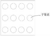
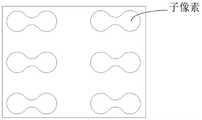
在其中一个实施例中,所述像素定义层上形成有像素开口;所述像素开口用于定义子像素的形状;所述子像素的形状为圆形、椭圆形或者哑铃形。In one embodiment, a pixel opening is formed on the pixel defining layer; the pixel opening is used to define the shape of the sub-pixel; the shape of the sub-pixel is a circle, an ellipse or a dumbbell shape.
在其中一个实施例中,所述隔离结构在所述基板上的投影的边与所述像素开口在所述基板上的投影的边互不平行。In one embodiment, the side of the projection of the isolation structure on the substrate and the side of the projection of the pixel opening on the substrate are not parallel to each other.
在其中一个实施例中,在所述基板表面所在平面上,不同层体结构在所述基板上的投影的波峰错开或者不同层体结构在所述基板上的投影的波谷错开。In one embodiment, on the plane where the surface of the substrate is located, the peaks of projections of different layer structures on the substrate are staggered or the troughs of projections of different layer structures on the substrate are staggered.
在其中一个实施例中,所述显示面板为PMOLED显示面板;所述隔离结构包括第一隔离层和第二隔离层;所述第一隔离层的底面与所述像素定义层接触;所述第一隔离层的顶面与所述第二隔离层的底面接触;所述第二隔离层的顶面与其底面相对设置;所述第二隔离层的底面宽度大于所述第一隔离层的顶面宽度;和/或In one embodiment, the display panel is a PMOLED display panel; the isolation structure includes a first isolation layer and a second isolation layer; the bottom surface of the first isolation layer is in contact with the pixel definition layer; the first isolation layer The top surface of an isolation layer is in contact with the bottom surface of the second isolation layer; the top surface of the second isolation layer is disposed opposite to its bottom surface; the width of the bottom surface of the second isolation layer is greater than that of the first isolation layer width; and/or
所述第一隔离层的纵截面为梯形;所述第二隔离层的纵截面为矩形;所述第二隔离层的底面和顶面具有相同的形状;所述第二隔离层的顶面在所述基板上的投影与所述第一隔离层的底面在所述基板上的投影相互错开;所述纵截面垂直于所述基板表面。The longitudinal section of the first isolation layer is a trapezoid; the longitudinal section of the second isolation layer is a rectangle; the bottom surface and the top surface of the second isolation layer have the same shape; the top surface of the second isolation layer is in the The projection on the substrate and the projection of the bottom surface of the first isolation layer on the substrate are offset from each other; the longitudinal section is perpendicular to the surface of the substrate.
一种显示屏,具有至少一个显示区;所述至少一个显示区包括第一显示区,所述第一显示区下方可设置感光器件;A display screen with at least one display area; the at least one display area includes a first display area, and a photosensitive device can be arranged under the first display area;
其中,在所述第一显示区设置有如前述任一实施例所述的显示面板,所述至少一个显示区中各显示区均用于显示动态或静态画面。Wherein, the first display area is provided with the display panel according to any of the foregoing embodiments, and each display area in the at least one display area is used for displaying dynamic or static images.
在其中一个实施例中,所述至少一个显示区还包括第二显示区;在所述第一显示区设置的显示面板为PMOLED显示面板或AMOLED显示面板,在所述第二显示区设置的显示面板为AMOLED显示面板。In one embodiment, the at least one display area further includes a second display area; the display panel arranged in the first display area is a PMOLED display panel or an AMOLED display panel, and the display panel arranged in the second display area is a PMOLED display panel or an AMOLED display panel. The panel is an AMOLED display panel.
一种显示终端,包括:A display terminal including:
设备本体,具有器件区;The device body has a device area;
如前述任一实施例所述的显示屏,覆盖在所述设备本体上;The display screen according to any one of the preceding embodiments is covered on the device body;
其中,所述器件区位于所述第一显示区下方,且所述器件区中设置有透过所述第一显示区进行光线采集的感光器件。Wherein, the device area is located below the first display area, and a photosensitive device for collecting light through the first display area is disposed in the device area.
附图说明Description of drawings
图1为传统的显示面板的剖视图;1 is a cross-sectional view of a conventional display panel;
图2为图1中的隔离柱的俯视图;Fig. 2 is the top view of the isolation column in Fig. 1;
图3为一实施例中的显示面板的剖视图;3 is a cross-sectional view of a display panel in an embodiment;
图4为一实施例中的隔离结构在基板上的投影的示意图;4 is a schematic diagram of a projection of an isolation structure on a substrate in an embodiment;
图5为另一实施例中的隔离结构在基板上的投影的示意图;5 is a schematic diagram of a projection of an isolation structure on a substrate in another embodiment;
图6为又一实施例中的隔离结构在基板上的投影的示意图;6 is a schematic diagram of a projection of an isolation structure on a substrate in yet another embodiment;
图7为一实施例中的子像素的形状示意图;7 is a schematic diagram of the shape of a sub-pixel in an embodiment;
图8为另一实施例中的子像素的形状示意图;8 is a schematic diagram of the shape of a sub-pixel in another embodiment;
图9为再一实施例中的子像素的形状示意图;9 is a schematic diagram of the shape of a sub-pixel in yet another embodiment;
图10为一实施例中的显示屏的结构示意图;10 is a schematic structural diagram of a display screen in an embodiment;
图11为一实施例中的显示终端的结构示意图;11 is a schematic structural diagram of a display terminal in an embodiment;
图12为一实施例中的设备本体的结构示意图。FIG. 12 is a schematic structural diagram of a device body in an embodiment.
具体实施方式Detailed ways
为了使本发明的目的、技术方案及优点更加清楚明白,以下结合附图及实施例,对本发明进行进一步详细说明。应当理解,此处所描述的具体实施例仅仅用以解释本发明,并不用于限定本发明。In order to make the objectives, technical solutions and advantages of the present invention clearer, the present invention will be further described in detail below with reference to the accompanying drawings and embodiments. It should be understood that the specific embodiments described herein are only used to explain the present invention, but not to limit the present invention.
在本发明的描述中,需要理解的是,术语“中心”、“横向”、“上”、“下”“左”、“右”、“竖直”、“水平”、“顶”、“底”、“内”以及“外”等指示的方位或位置关系为基于附图所示的方位或位置关系,仅是为了便于描述本发明和简化描述,而不是指示或暗示所指的装置或元件必须具有特定的方位、以特定的方位构造和操作,因此不能理解为对本发明的限制。此外,需要说明的是,当元件被称为“形成在另一元件上”时,它可以直接连接到另一元件上或者可能同时存在居中元件。当一个元件被认为是“连接”另一个元件,它可以直接连接到另一元件或者同时存在居中元件。相反,当元件被称作“直接在”另一元件“上”时,不存在中间元件。In the description of the present invention, it should be understood that the terms "center", "lateral", "top", "bottom", "left", "right", "vertical", "horizontal", "top", " The orientation or positional relationship indicated by "bottom", "inner" and "outer" is based on the orientation or positional relationship shown in the accompanying drawings, and is only for the convenience of describing the present invention and simplifying the description, rather than indicating or implying the indicated device or position. Elements must have a particular orientation, be constructed and operate in a particular orientation and are therefore not to be construed as limitations of the invention. Also, it will be noted that when an element is referred to as being "formed on" another element, it can be directly connected to the other element or intervening elements may also be present. When an element is considered to be "connected" to another element, it can be directly connected to the other element or intervening elements may also be present. In contrast, when an element is referred to as being "directly on" another element, there are no intervening elements present.
正如背景技术所述,将摄像头等感光器件设置在透明显示面板下方时,拍照得到的照片模糊。发明人研究发现,出现这个问题的原因在于,由于电子设备的显示屏体内存在导电走线,外部光线经过这些导电走线时会造成较为复杂的衍射强度分布,从而出现衍射条纹,进而会影响摄像头等感光器件的正常工作。例如,位于透明显示区域之下的摄像头工作时,外部光线经过显示屏内的导线材料走线后会发生较为明显的衍射,从而使得摄像头拍摄到的画面出现失真的问题。As described in the background art, when a photosensitive device such as a camera is arranged under the transparent display panel, the photos obtained by taking pictures are blurred. The inventor's research found that the reason for this problem is that due to the presence of conductive traces in the display screen of the electronic device, when the external light passes through these conductive traces, it will cause a relatively complex diffraction intensity distribution, resulting in diffraction fringes, which will affect the camera. Wait for the photosensitive device to work normally. For example, when the camera located under the transparent display area is working, the external light will be significantly diffracted after passing through the wire material in the display screen, so that the picture captured by the camera will be distorted.
为解决上述问题,本申请一实施例提供了一种显示面板,其能够很好地解决上述问题。一实施例中的显示面板包括基板、形成于基板上的像素定义层以及形成于像素定义层上的隔离结构。其中,像素定义层上形成有像素开口。像素开口用于定义子像素的形状。隔离结构用于将相邻两行或者两列子像素的阴极进行隔离,并对相邻两行或者两列子像素的阴极形状起到限定作用。In order to solve the above problems, an embodiment of the present application provides a display panel, which can well solve the above problems. A display panel in an embodiment includes a substrate, a pixel definition layer formed on the substrate, and an isolation structure formed on the pixel definition layer. Wherein, pixel openings are formed on the pixel definition layer. The pixel openings are used to define the shape of the sub-pixels. The isolation structure is used to isolate the cathodes of the sub-pixels in two adjacent rows or columns, and plays a role in limiting the shape of the cathodes of the sub-pixels in the adjacent two rows or columns.
在本实施例中,隔离结构包括沿垂直于基板表面的方向上依次层叠的两层以上的层体结构。例如,隔离结构可以包括沿垂直于基板的方向上依次层叠的第一隔离层和第二隔离层。在其他的实施例中,隔离结构还可以包括三层以上的层体结构。在隔离结构的延伸方向上,两层以上的层体结构中至少有一层的层体结构的宽度持续变化或者间隔性变化。隔离结构的延伸方向平行于基板表面,也即隔离结构的长度方向,其宽度方向则垂直于长度方向。前面提及的宽度为在基板表面所在的平面上,隔离结构在基板上的投影在垂直于延伸方向上的尺寸。由于隔离结构为立体结构,在其垂直于基板的截面上(也即纵截面),不同高度位置处可能具有不同的宽度。因此,本实施例中所指的隔离结构的宽度对应于在纵截面中的最大宽度。In this embodiment, the isolation structure includes a layered structure of two or more layers stacked in sequence along a direction perpendicular to the surface of the substrate. For example, the isolation structure may include a first isolation layer and a second isolation layer sequentially stacked in a direction perpendicular to the substrate. In other embodiments, the isolation structure may further include a layered structure with more than three layers. In the extending direction of the isolation structure, the width of at least one layer of the two or more layer structures continuously changes or changes intermittently. The extension direction of the isolation structure is parallel to the surface of the substrate, that is, the length direction of the isolation structure, and the width direction of the isolation structure is perpendicular to the length direction. The width mentioned above is the dimension perpendicular to the extending direction of the projection of the isolation structure on the substrate on the plane of the substrate surface. Since the isolation structure is a three-dimensional structure, on its section perpendicular to the substrate (ie, the longitudinal section), different height positions may have different widths. Therefore, the width of the isolation structure referred to in this embodiment corresponds to the maximum width in the longitudinal section.
由于隔离结构为立体结构,其各层的层体结构同样为立体结构。因此,在隔离结构的纵截面(也即垂直于基板的截面),不同高度位置处可能具有不同的宽度。当外部光线经过各层的层体结构时,会发生衍射现象。衍射是指光遇到障碍物时偏离直线传播的物理现象。具体地,光波在经过狭缝、小孔或者圆盘之类的障碍物后发生不同程度的弯散传播。因此,当外部光线经过隔离结构时,会产生类似于狭缝衍射的衍射条纹,其衍射条纹的位置由各处的最大宽度决定。因此,控制隔离结构中至少有一层的层体结构在延伸方向上的宽度连续或者间隔性变化,则可以使得光线经过给隔离结构时,能够在不同宽度位置处产生具有不同位置的衍射条纹,进而减弱衍射效应,达到改善衍射的效果。Since the isolation structure is a three-dimensional structure, the layer structure of each layer is also a three-dimensional structure. Therefore, in the longitudinal section of the isolation structure (ie, the section perpendicular to the substrate), different height positions may have different widths. Diffraction occurs when external light passes through the layered structure of each layer. Diffraction is the physical phenomenon in which light travels away from a straight line when it encounters an obstacle. Specifically, after passing through obstacles such as slits, small holes or discs, light waves undergo different degrees of bending and scattering propagation. Therefore, when external light passes through the isolation structure, diffraction fringes similar to slit diffraction are generated, and the position of the diffraction fringes is determined by the maximum width everywhere. Therefore, by controlling the width of the layer structure of at least one layer in the isolation structure in the extending direction to change continuously or intermittently, when the light passes through the isolation structure, diffraction fringes with different positions can be generated at different width positions, and further The diffraction effect is weakened to achieve the effect of improving the diffraction.
传统的隔离柱通常为条状,其俯视图如图3所示,其剖视图可以参见图2。传统的隔离柱的纵截面(也即垂直于基板的截面)为倒梯形结构。具体地,其具有与基板相接触的底面以及与该底面相对的顶面。隔离柱从顶面至底面呈渐缩状,从而使得隔离柱的最大宽度出现在顶面。顶面为长方形,其沿延伸方向具有固定不变的宽度(也即在延伸方向上各处的宽度相同,延伸方向均为平行于基板的方向)。隔离柱上具有相同宽度位置处产生的衍射条纹的位置相同,从而使得衍射效果较为明显,最终影响位于其下方的感光元件的正常工作,例如会使得摄像头拍摄到的画面失真。The traditional isolation column is usually strip-shaped, and its top view is shown in FIG. 3 , and its cross-sectional view can be seen in FIG. 2 . The longitudinal section (ie, the section perpendicular to the substrate) of the conventional isolation column is an inverted trapezoid structure. Specifically, it has a bottom surface in contact with the substrate and a top surface opposite to the bottom surface. The spacers taper from the top to the bottom, so that the maximum width of the spacers occurs at the top. The top surface is a rectangle with a constant width along the extending direction (that is, the width is the same everywhere in the extending direction, and the extending directions are all parallel to the substrate). The diffraction fringes generated at positions with the same width on the isolation column are in the same position, so that the diffraction effect is more obvious, which ultimately affects the normal operation of the photosensitive element located below it, for example, the picture captured by the camera will be distorted.
本申请上述实施例中的显示面板,通过采用在延伸方向上宽度连续变化或者间断变化的具有至少两层的层体结构的隔离结构,在不同最大宽度位置处产生的衍射条纹的位置不同,可以破坏传统的隔离柱所带来的复杂的衍射强度分布,从而使得衍射相对不那么明显,达到改善衍射的效果。In the display panel in the above-mentioned embodiments of the present application, by adopting an isolation structure with a layered structure with at least two layers whose width continuously changes or intermittently changes in the extending direction, the positions of diffraction fringes generated at different maximum width positions are different. The complex diffraction intensity distribution brought about by the traditional isolation column is destroyed, so that the diffraction is relatively less obvious, and the effect of improving the diffraction is achieved.
在一实施例中,在隔离结构的延伸方向上,各层体结构的宽度均持续变化或者间隔性变化,从而确保显示面板在平行于基板的水平面上均具有较好的衍射改善效果,进而使得整个显示面板具有较好的衍射改善效果。In one embodiment, in the extending direction of the isolation structure, the width of each layer structure continuously changes or changes at intervals, so as to ensure that the display panel has a better diffraction improvement effect on the horizontal plane parallel to the substrate, thereby making The entire display panel has a better diffraction improvement effect.
在一实施例中,在隔离结构的延伸方向上,各层体结构在基板上的投影为波浪形,也即其在延伸方向上的宽度连续变化,从而能够打破隔离结构在延伸方向上的宽度均匀性分布,以降低衍射效应。在一实施例中,各层层体结构沿延伸方向均具有对称结构,从而可以简化制备工艺过程。In one embodiment, in the extension direction of the isolation structure, the projection of each layer structure on the substrate is a wave shape, that is, its width in the extension direction changes continuously, so that the width of the isolation structure in the extension direction can be broken. Uniform distribution to reduce diffraction effects. In one embodiment, each layer structure has a symmetrical structure along the extending direction, so that the manufacturing process can be simplified.
在一实施例中,在基板表面所在的平面上,不同层体结构在基板上的投影的波峰错开或者不同层体结构在基板上的波谷相互错开,从而进一步打乱隔离结构在延伸方向上的最大宽度的均匀性分布。因此,当外部光线经过该隔离结构时,在不同位置处产生的衍射条纹的位置不同,从而可以有效减弱衍射效应,达到改善衍射的效果。In one embodiment, on the plane where the surface of the substrate is located, the peaks of projections of different layer structures on the substrate are staggered or the troughs of different layer structures on the substrate are staggered, thereby further disrupting the isolation structure in the extension direction. Uniform distribution of the maximum width. Therefore, when the external light passes through the isolation structure, the positions of the diffraction fringes generated at different positions are different, so that the diffraction effect can be effectively weakened and the effect of improving the diffraction can be achieved.
图3为一实施例中的显示面板的剖视图。该显示面板为PMOELD显示面板。该显示面板包括基板110、形成于基板110上的像素定义层120以及形成于像素定义层120上的隔离结构130。在本实施例中,隔离结构130包括依次层叠的第一隔离层132和第二隔离层134。第一隔离层132的底面132a与像素定义层120连接。第一隔离层132的顶面132b与第二隔离层134的底面134a连接。FIG. 3 is a cross-sectional view of a display panel in an embodiment. The display panel is a PMOELD display panel. The display panel includes a
在一实施例中,在隔离结构130的纵截面(也即垂直于基板110的方向上的截面),第一隔离层132的顶面132b的宽度小于第二隔离层134的底面134a的宽度,从而在垂直于基板110表面的方向上,不同高度处的衍射条纹的位置不同,不同位置的衍射条纹相互抵消,从而降低衍射效应。In one embodiment, in the longitudinal section of the isolation structure 130 (that is, the section in the direction perpendicular to the substrate 110 ), the width of the
在一实施例中,在隔离结构130的纵截面上,第一隔离层132的截面为梯形,第二隔离层134的截面为矩形。具体地,第一隔离层132的顶面132b的宽度大于底面132a的宽度,从而形成正向放置的梯形结构。第二隔离层134则为矩形,也即其顶面134b与底面134a具有相同的宽度。第二隔离层134的顶面134b与底面134a具有相同的形状。在本实施例中,第二隔离层134的顶面134b具有与第一隔离层132的底面132a不同的形状。具体地,隔离结构130中的第一隔离层132和第二隔离层134在基板上的投影均为波浪形,如图4所示。其中,填充区域为第二隔离结构层134投影在基板110上的形状。此时,第一隔离层132在基板110上的投影的波峰T1与第二隔离层134在基板110上的投影的波峰T2错开设置,且第一隔离层132在基板110上的投影的波谷B1与第二隔离层134在基板110上的投影的波谷B2错开,从而进一步打乱隔离结构130在延伸方向上的宽度的均匀性分布,从而降低衍射效应。In one embodiment, on the longitudinal section of the
参见图3,第一隔离层132和第二隔离层134的高度之和等于传统的单层隔离结构的高度。在一实施例中,可以控制第一个隔离层132的高度H11与第二隔离层134的高度H22之比为4:1。第一个隔离层132的高度H11与第二隔离层134的高度H22之比并没有特别要求,满足工艺制备能力即可。在本实施例中,隔离结构130也即第一隔离层132的底面的最大宽度或者第二隔离层134的最大宽度W22通常为10微米左右。相邻两个隔离结构130的间距W11一般根据子像素大小进行定义,如可以将其设置为大于或等于90微米。Referring to FIG. 3 , the sum of the heights of the
图4所示的实施例中,第一隔离层132和第二隔离层134在基板110的投影均为波浪形,在其他的实施例中,第一隔离结构132和第二隔离结构134在基板110上的投影可以均为锯齿状,如图5所示。同样地,填充区域为第二隔离层134在基板110上的投影。在又一实施例中国,也可以另其中一个隔离结构层的投影为波浪形,而另外一个为锯齿状,只需要二者的凸起部位错开或者凹陷部位错开即可,如图6所示。In the embodiment shown in FIG. 4 , the projections of the
在一实施例中,像素定义层120上形成有像素开口。像素开口用于定义子像素的形状。像素开口在基板11上的投影的各边均为曲线,且各边互不平行,也即子像素的各边为互不平行的曲线。在一实施例中,子像素的形状为圆形如图7所示。在另一实施例中,子像素的形状可以为椭圆形,如图8所示。子像素的形状还可以为哑铃形,如图9所示。通过将子像素的形状设置成圆形、椭圆形或者哑铃形,也即位于像素开口内的有机发光层150为圆形、椭圆形或者哑铃形,从而使得光线经过该有机发光层150时,在不同宽度的位置处产生不同位置和发散方向的沿河条纹,从而降低衍射效应。In one embodiment, pixel openings are formed on the
在一实施例中,隔离结构130在基板110上的投影与像素开口也即有机发光层150在基板110上的投影的边缘互不平行,从而使得二者的边缘间距并不固定唯一,进而确保在不同间距位置处产生不同位置的衍射条纹,最终降低衍射效应。In one embodiment, the projection of the
在一实施例中,上述显示面板为PMOLED显示面板时,还包括形成于基板上的阳极层140以及形成于有机发光层150上的阴极层160。有机发光层150形成在阳极层140上方,如图1所示。在一实施例中,为了提高显示面板的透光率,如阳极层140和阴极层160采用透明导电金属氧化物制备而成。举例来说,阳极层140和阴极层160可以采用ITO(氧化铟锡)或氧化铟锌(IZ0)制成。进一步的,为了在保证高透光率的基础上,减小各导电走线的电阻,阳极层140和阴极层160还可以采用铝掺杂氧化锌、掺杂银的ITO或者掺杂银的IZ0等材料制成。In one embodiment, when the above-mentioned display panel is a PMOLED display panel, it further includes an
在一实施例中,隔离结构130的各层体结构在延伸方向上做周期性的宽度变化。具体地,可以每个子像素对应相同的层体结构的侧边。通过将宽度设置为周期性变化,可以确保显示面板上各处的像素发光亮度的均匀性,从而不影响显示面板的显示效果。在其他的实施例中,其宽度变化也可以为不规则变化,此时具有较好的衍射改善效果。In one embodiment, each layer structure of the
在一实施例中,上述显示面板可以为透明或者半透半反式的显示面板。显示面板的透明可以通过采用透光率较好的各层材料来实现。例如,除阻光层外均采用透光率大于90%的材料,从而使得整个显示面板的透光率可以在70%以上。进一步的,各透明功能层均采用透光率大于95%的材料,进一步提高显示面板的透光率,甚至使得整个显示面板的透光率在80%以上。具体地,可以将导电走线如阴极和阳极等设置为ITO、IZO、Ag+ITO或者Ag+IZO等,绝缘层材料优选SiO2,SiNx以及Al2O3等,像素定义层则采用高透明材料。In one embodiment, the above-mentioned display panel may be a transparent or transflective display panel. The transparency of the display panel can be achieved by using various layers of materials with better light transmittance. For example, materials with a light transmittance greater than 90% are used except for the light blocking layer, so that the light transmittance of the entire display panel can be above 70%. Further, each transparent functional layer adopts a material with a light transmittance greater than 95%, which further improves the light transmittance of the display panel, and even makes the light transmittance of the entire display panel above 80%. Specifically, the conductive traces such as cathode and anode can be set as ITO, IZO, Ag+ITO or Ag+IZO, etc., the insulating layer material is preferably SiO2 , SiNx and Al2 O3 , etc., and the pixel definition layer is made of high Transparent material.
在一实施例中,基板可以为刚性基板或柔性基板,如刚性基板可选择玻璃基板、石英基板或者塑料基板等透明基板,柔性基板可选择柔性PI基板等。In one embodiment, the substrate may be a rigid substrate or a flexible substrate, for example, a transparent substrate such as a glass substrate, a quartz substrate or a plastic substrate may be selected for the rigid substrate, and a flexible PI substrate may be selected for the flexible substrate.
可以理解,显示面板的透明还可以采用其他技术手段实现,上述显示面板的结构均可以适用。透明或者半透半反式的显示面板处于工作状态时能够正常显示画面,而当显示面板处于其他功能需求状态时,外部光线可以透过该显示面板照射到置于该显示面板之下的感光器件等。It can be understood that the transparency of the display panel can also be achieved by other technical means, and the above-mentioned structures of the display panel are all applicable. The transparent or transflective display panel can display the picture normally when it is in working state, and when the display panel is in other functional requirements state, the external light can pass through the display panel and irradiate the photosensitive device placed under the display panel. Wait.
图10为一实施例中的显示屏的结构示意图,该显示屏包括第一显示区910和第二显示区920。可以理解,第一显示区910和第二显示区920并不是只有一个显示区,只是两种类型的显示区的区分。其中,第一显示区910的透光率大于第二显示区920的透光率。第一显示区910的下方可设置感光器件930。第一显示区910设置有如前述任一实施例中所提及的显示面板。第一显示区910和第二显示区920均用于显示静态或者动态画面。由于第一显示区910采用了前述实施例中的显示面板,因此当光线经过该显示区域时,不会产生较为明显的衍射效应,从而能够确保位于该第一显示区910下方的感光器件930能够正常工作。可以理解,第一显示区910在感光器件930不工作时,可以正常进行动态或者静态画面显示,而在感光器件930工作时,可以处于不显示状态,从而确保感光器件930能够透过该显示面板正常进行光线采集。在其他的实施例中,第一显示区910和第二显示区920的透光率也可以相同,从而使得整个显示面板具有较好的透光均一性,确保显示面板具有较好的显示效果。FIG. 10 is a schematic structural diagram of a display screen in an embodiment. The display screen includes a
在一实施例中,第一显示区910设置的显示面板为PMOLED显示面板或AMOLED显示面板,在第二显示区920设置的显示面板为AMOLED显示面板,从而形成由PMOLED显示面板和MOLED显示面板构成的全面屏。In one embodiment, the display panel provided in the
本申请另一实施例还提供一种显示终端。图11为一实施例中的显示终端的结构示意图,该显示终端包括设备本体810和显示屏820。显示屏820设置在设备本体810上,且与该设备本体810相互连接。其中,显示屏820可以采用前述任一实施例中的显示屏,用以显示静态或者动态画面。Another embodiment of the present application also provides a display terminal. FIG. 11 is a schematic structural diagram of a display terminal in an embodiment, where the display terminal includes a
图12为一实施例中的设备本体810的结构示意图。在本实施例中,设备本体810上可设有开槽区812和非开槽区814。在开槽区812中可设置有诸如摄像头930以及光传感器等感光器件。此时,显示屏820的第一显示区的显示面板对应于开槽区814贴合在一起,以使得上述的诸如摄像头930及光传感器等感光器件能够透过该第一显示区对外部光线进行采集等操作。由于第一显示区中的显示面板能够有效改善外部光线透射该第一显示区所产生的衍射现象,从而可有效提升显示设备上摄像头930所拍摄图像的质量,避免因衍射而导致所拍摄的图像失真,同时也能提升光传感器感测外部光线的精准度和敏感度。FIG. 12 is a schematic structural diagram of a
上述电子设备可以为手机、平板、掌上电脑、ipod等数码设备。The above-mentioned electronic device may be a digital device such as a mobile phone, a tablet, a handheld computer, and an ipod.
以上所述实施例的各技术特征可以进行任意的组合,为使描述简洁,未对上述实施例中的各个技术特征所有可能的组合都进行描述,然而,只要这些技术特征的组合不存在矛盾,都应当认为是本说明书记载的范围。The technical features of the above-described embodiments can be combined arbitrarily. For the sake of brevity, all possible combinations of the technical features in the above-described embodiments are not described. However, as long as there is no contradiction between the combinations of these technical features, All should be regarded as the scope described in this specification.
以上所述实施例仅表达了本发明的几种实施方式,其描述较为具体和详细,但并不能因此而理解为对发明专利范围的限制。应当指出的是,对于本领域的普通技术人员来说,在不脱离本发明构思的前提下,还可以做出若干变形和改进,这些都属于本发明的保护范围。因此,本发明专利的保护范围应以所附权利要求为准。The above-mentioned embodiments only represent several embodiments of the present invention, and the descriptions thereof are specific and detailed, but should not be construed as a limitation on the scope of the invention patent. It should be pointed out that for those of ordinary skill in the art, without departing from the concept of the present invention, several modifications and improvements can also be made, which all belong to the protection scope of the present invention. Therefore, the protection scope of the patent of the present invention should be subject to the appended claims.
Claims (10)
Translated fromChinesePriority Applications (3)
| Application Number | Priority Date | Filing Date | Title |
|---|---|---|---|
| CN201810887040.0ACN110767674B (en) | 2018-08-06 | 2018-08-06 | Display panel, display screen and display terminal |
| PCT/CN2019/084862WO2020029612A1 (en) | 2018-08-06 | 2019-04-28 | Display panel, display screen, and display terminal |
| US16/923,089US11296184B2 (en) | 2018-08-06 | 2020-07-08 | Display panels, display screens, and display terminals |
Applications Claiming Priority (1)
| Application Number | Priority Date | Filing Date | Title |
|---|---|---|---|
| CN201810887040.0ACN110767674B (en) | 2018-08-06 | 2018-08-06 | Display panel, display screen and display terminal |
Publications (2)
| Publication Number | Publication Date |
|---|---|
| CN110767674A CN110767674A (en) | 2020-02-07 |
| CN110767674Btrue CN110767674B (en) | 2022-05-17 |
Family
ID=69328888
Family Applications (1)
| Application Number | Title | Priority Date | Filing Date |
|---|---|---|---|
| CN201810887040.0AActiveCN110767674B (en) | 2018-08-06 | 2018-08-06 | Display panel, display screen and display terminal |
Country Status (3)
| Country | Link |
|---|---|
| US (1) | US11296184B2 (en) |
| CN (1) | CN110767674B (en) |
| WO (1) | WO2020029612A1 (en) |
Families Citing this family (17)
| Publication number | Priority date | Publication date | Assignee | Title |
|---|---|---|---|---|
| KR20180075589A (en) | 2015-10-26 | 2018-07-04 | 오티아이 루미오닉스 인크. | A method of patterning a coating on a surface and a device comprising a patterned coating |
| JP7056964B2 (en) | 2016-12-02 | 2022-04-19 | オーティーアイ ルミオニクス インコーポレーテッド | Devices with conductive coatings placed over the radiating region and methods for them |
| JP2020518107A (en) | 2017-04-26 | 2020-06-18 | オーティーアイ ルミオニクス インコーポレーテッドOti Lumionics Inc. | Method for patterning a coating on a surface and device containing the patterned coating |
| CN110832660B (en) | 2017-05-17 | 2023-07-28 | Oti照明公司 | Method for selectively depositing conductive coating on patterned coating and device comprising conductive coating |
| CN107425045A (en)* | 2017-09-18 | 2017-12-01 | 京东方科技集团股份有限公司 | A kind of manufacture method of array base palte, display device and array base palte |
| US11751415B2 (en) | 2018-02-02 | 2023-09-05 | Oti Lumionics Inc. | Materials for forming a nucleation-inhibiting coating and devices incorporating same |
| KR20240134065A (en) | 2018-11-23 | 2024-09-05 | 오티아이 루미오닉스 인크. | Optoelectronic device including a light transmissive region |
| CN109801950B (en)* | 2019-01-31 | 2021-02-26 | 厦门天马微电子有限公司 | Display panel, display device and manufacturing method of display panel |
| CN116456753A (en) | 2019-03-07 | 2023-07-18 | Oti照明公司 | an optoelectronic device |
| KR102831863B1 (en) | 2019-04-18 | 2025-07-10 | 오티아이 루미오닉스 인크. | Material for forming a nucleation-inhibiting coating and device comprising the same |
| CN114072705A (en) | 2019-05-08 | 2022-02-18 | Oti照明公司 | Material for forming nucleation inhibiting coatings and apparatus incorporating the same |
| JP7386556B2 (en) | 2019-06-26 | 2023-11-27 | オーティーアイ ルミオニクス インコーポレーテッド | Optoelectronic devices containing optically transparent regions with applications related to optical diffraction properties |
| US11832473B2 (en) | 2019-06-26 | 2023-11-28 | Oti Lumionics Inc. | Optoelectronic device including light transmissive regions, with light diffraction characteristics |
| CN114342068A (en) | 2019-08-09 | 2022-04-12 | Oti照明公司 | Optoelectronic device containing auxiliary electrodes and partitions |
| KR20220131245A (en) | 2019-12-24 | 2022-09-27 | 오티아이 루미오닉스 인크. | Light emitting device including capping layer and manufacturing method thereof |
| US12113279B2 (en) | 2020-09-22 | 2024-10-08 | Oti Lumionics Inc. | Device incorporating an IR signal transmissive region |
| CN113488602B (en)* | 2021-07-26 | 2023-10-03 | 合肥维信诺科技有限公司 | Display panel and preparation method thereof |
Citations (12)
| Publication number | Priority date | Publication date | Assignee | Title |
|---|---|---|---|---|
| JPH11339958A (en)* | 1998-05-22 | 1999-12-10 | Casio Comput Co Ltd | Method for manufacturing electroluminescent device |
| CN1631057A (en)* | 2002-02-08 | 2005-06-22 | 日本瑞翁株式会社 | Coating film for organic electroluminescence device, organic electroluminescence device using the coating film, and method for preparing the device |
| CN1697583A (en)* | 2004-05-11 | 2005-11-16 | 松下电器产业株式会社 | Light emitting device and display device |
| CN102130300A (en)* | 2010-09-16 | 2011-07-20 | 昆山维信诺显示技术有限公司 | Organic electroluminescent device (OELD), display and application thereof |
| CN102290430A (en)* | 2010-06-16 | 2011-12-21 | 索尼公司 | Display device |
| EP2503621A1 (en)* | 2011-03-24 | 2012-09-26 | Moser Baer India Ltd. | A barrier layer and a method of manufacturing the barrier layer |
| CN104766933A (en)* | 2015-04-30 | 2015-07-08 | 京东方科技集团股份有限公司 | Isolation column and its manufacturing method, display panel and display device |
| CN106367716A (en)* | 2015-07-24 | 2017-02-01 | 上海和辉光电有限公司 | Mask plate and display panel production method |
| CN106920821A (en)* | 2015-12-24 | 2017-07-04 | 株式会社日本显示器 | Display device |
| CN107170905A (en)* | 2017-07-05 | 2017-09-15 | 固安翌光科技有限公司 | A kind of highly reliable passive organic electroluminescent device and preparation method thereof |
| CN107275377A (en)* | 2017-06-28 | 2017-10-20 | 武汉华星光电半导体显示技术有限公司 | OLED and display device |
| CN107507522A (en)* | 2017-08-29 | 2017-12-22 | 京东方科技集团股份有限公司 | Display panel and display device |
Family Cites Families (8)
| Publication number | Priority date | Publication date | Assignee | Title |
|---|---|---|---|---|
| US6699728B2 (en)* | 2000-09-06 | 2004-03-02 | Osram Opto Semiconductors Gmbh | Patterning of electrodes in oled devices |
| KR100421720B1 (en)* | 2001-12-13 | 2004-03-11 | 삼성 엔이씨 모바일 디스플레이 주식회사 | Electro luminescence device and method of manufacturing the same |
| ITUD20020059A1 (en)* | 2002-03-12 | 2003-09-12 | Seima Italiana Spa | OPTICAL LIGHTING DEVICE AND METHOD OF PRODUCTION OF LIGHTING DEVICES OR SIMILAR ADOPTING SUCH DEVICE |
| KR100768711B1 (en)* | 2006-05-04 | 2007-10-19 | 주식회사 대우일렉트로닉스 | Organic electroluminescent device and manufacturing method thereof |
| CN105118929B (en) | 2015-08-03 | 2018-01-02 | 京东方科技集团股份有限公司 | Electrode structure and organic light-emitting units and its manufacture method |
| US10651242B2 (en) | 2017-06-28 | 2020-05-12 | Wuhan China Star Optoelectronics Semiconductor Display Technology Co., Ltd. | OLED device and display apparatus |
| CN110767677B (en)* | 2018-08-06 | 2025-06-27 | 云谷(固安)科技有限公司 | Display panel, display screen and display terminal |
| CN208608202U (en)* | 2018-08-06 | 2019-03-15 | 云谷(固安)科技有限公司 | Display panel, display screen and display terminal |
- 2018
- 2018-08-06CNCN201810887040.0Apatent/CN110767674B/enactiveActive
- 2019
- 2019-04-28WOPCT/CN2019/084862patent/WO2020029612A1/ennot_activeCeased
- 2020
- 2020-07-08USUS16/923,089patent/US11296184B2/enactiveActive
Patent Citations (12)
| Publication number | Priority date | Publication date | Assignee | Title |
|---|---|---|---|---|
| JPH11339958A (en)* | 1998-05-22 | 1999-12-10 | Casio Comput Co Ltd | Method for manufacturing electroluminescent device |
| CN1631057A (en)* | 2002-02-08 | 2005-06-22 | 日本瑞翁株式会社 | Coating film for organic electroluminescence device, organic electroluminescence device using the coating film, and method for preparing the device |
| CN1697583A (en)* | 2004-05-11 | 2005-11-16 | 松下电器产业株式会社 | Light emitting device and display device |
| CN102290430A (en)* | 2010-06-16 | 2011-12-21 | 索尼公司 | Display device |
| CN102130300A (en)* | 2010-09-16 | 2011-07-20 | 昆山维信诺显示技术有限公司 | Organic electroluminescent device (OELD), display and application thereof |
| EP2503621A1 (en)* | 2011-03-24 | 2012-09-26 | Moser Baer India Ltd. | A barrier layer and a method of manufacturing the barrier layer |
| CN104766933A (en)* | 2015-04-30 | 2015-07-08 | 京东方科技集团股份有限公司 | Isolation column and its manufacturing method, display panel and display device |
| CN106367716A (en)* | 2015-07-24 | 2017-02-01 | 上海和辉光电有限公司 | Mask plate and display panel production method |
| CN106920821A (en)* | 2015-12-24 | 2017-07-04 | 株式会社日本显示器 | Display device |
| CN107275377A (en)* | 2017-06-28 | 2017-10-20 | 武汉华星光电半导体显示技术有限公司 | OLED and display device |
| CN107170905A (en)* | 2017-07-05 | 2017-09-15 | 固安翌光科技有限公司 | A kind of highly reliable passive organic electroluminescent device and preparation method thereof |
| CN107507522A (en)* | 2017-08-29 | 2017-12-22 | 京东方科技集团股份有限公司 | Display panel and display device |
Non-Patent Citations (1)
| Title |
|---|
| 图形反转工艺制作OLED器件的阴极分离器;王军等;《发光学报》;20070415(第02期);198-202页* |
Also Published As
| Publication number | Publication date |
|---|---|
| WO2020029612A1 (en) | 2020-02-13 |
| US20200335576A1 (en) | 2020-10-22 |
| US11296184B2 (en) | 2022-04-05 |
| CN110767674A (en) | 2020-02-07 |
Similar Documents
| Publication | Publication Date | Title |
|---|---|---|
| CN110767674B (en) | Display panel, display screen and display terminal | |
| CN110767672B (en) | Display panel, display screen and display terminal | |
| US10903303B2 (en) | Display panel with a separation pillar having slanting side surfaces disposed on a pixel definition layer | |
| CN209071332U (en) | Display panel, display screen and display terminal | |
| CN110767825B (en) | Display panel, display screen and display terminal | |
| CN110808263B (en) | Display panel, display screen and display terminal | |
| WO2015180288A1 (en) | Embedded touch panel and display device | |
| CN110783481A (en) | Display panel, display screen and display device | |
| CN106896553A (en) | Display device with touch sensing function | |
| CN110767678B (en) | Display panel, display screen and display terminal | |
| WO2021189489A1 (en) | Array substrate and display apparatus | |
| WO2021189270A1 (en) | Array substrate and display device |
Legal Events
| Date | Code | Title | Description |
|---|---|---|---|
| PB01 | Publication | ||
| PB01 | Publication | ||
| SE01 | Entry into force of request for substantive examination | ||
| SE01 | Entry into force of request for substantive examination | ||
| CB02 | Change of applicant information | ||
| CB02 | Change of applicant information | Address after:215300, 188, Feng Feng Road, Kunshan hi tech Zone, Suzhou, Jiangsu, Kunshan Applicant after:Suzhou Qingyue Photoelectric Technology Co., Ltd Applicant after:Yungu (Gu'an) Technology Co.,Ltd. Applicant after:KunShan Go-Visionox Opto-Electronics Co.,Ltd. Address before:215300, 188, Feng Feng Road, Kunshan hi tech Zone, Suzhou, Jiangsu, Kunshan Applicant before:Kunshan Visionox Technology Co.,Ltd. Applicant before:Yungu (Gu'an) Technology Co.,Ltd. Applicant before:KunShan Go-Visionox Opto-Electronics Co.,Ltd. | |
| GR01 | Patent grant | ||
| GR01 | Patent grant |