CN110767621A - Packaged semiconductor element and method of making the same - Google Patents
Packaged semiconductor element and method of making the sameDownload PDFInfo
- Publication number
- CN110767621A CN110767621ACN201811209108.6ACN201811209108ACN110767621ACN 110767621 ACN110767621 ACN 110767621ACN 201811209108 ACN201811209108 ACN 201811209108ACN 110767621 ACN110767621 ACN 110767621A
- Authority
- CN
- China
- Prior art keywords
- insulating layer
- layer
- pad
- packaged semiconductor
- conductive
- Prior art date
- Legal status (The legal status is an assumption and is not a legal conclusion. Google has not performed a legal analysis and makes no representation as to the accuracy of the status listed.)
- Pending
Links
- 239000004065semiconductorSubstances0.000titleclaimsabstractdescription61
- 238000004519manufacturing processMethods0.000titleabstractdescription15
- 239000000523sampleSubstances0.000claimsabstractdescription40
- 238000001514detection methodMethods0.000claimsabstractdescription13
- 239000010410layerSubstances0.000claimsdescription269
- 239000000463materialSubstances0.000claimsdescription33
- 229910052751metalInorganic materials0.000claimsdescription28
- 239000002184metalSubstances0.000claimsdescription28
- 238000000034methodMethods0.000claimsdescription26
- 239000000758substrateSubstances0.000claimsdescription26
- RYGMFSIKBFXOCR-UHFFFAOYSA-NCopperChemical compound[Cu]RYGMFSIKBFXOCR-UHFFFAOYSA-N0.000claimsdescription14
- 229910052802copperInorganic materials0.000claimsdescription14
- 239000010949copperSubstances0.000claimsdescription14
- 239000011241protective layerSubstances0.000claimsdescription12
- 238000002360preparation methodMethods0.000claimsdescription11
- 239000004642PolyimideSubstances0.000claimsdescription7
- 229910052782aluminiumInorganic materials0.000claimsdescription7
- XAGFODPZIPBFFR-UHFFFAOYSA-NaluminiumChemical compound[Al]XAGFODPZIPBFFR-UHFFFAOYSA-N0.000claimsdescription7
- 229920001721polyimidePolymers0.000claimsdescription7
- MSNOMDLPLDYDME-UHFFFAOYSA-Ngold nickelChemical group[Ni].[Au]MSNOMDLPLDYDME-UHFFFAOYSA-N0.000claimsdescription6
- 238000005553drillingMethods0.000claimsdescription3
- 235000012431wafersNutrition0.000description12
- 238000005229chemical vapour depositionMethods0.000description6
- 238000000623plasma-assisted chemical vapour depositionMethods0.000description6
- 230000008901benefitEffects0.000description4
- 238000010586diagramMethods0.000description4
- 238000001039wet etchingMethods0.000description4
- PXHVJJICTQNCMI-UHFFFAOYSA-NNickelChemical compound[Ni]PXHVJJICTQNCMI-UHFFFAOYSA-N0.000description3
- 239000000203mixtureSubstances0.000description3
- 238000004528spin coatingMethods0.000description3
- 239000000126substanceSubstances0.000description3
- XUIMIQQOPSSXEZ-UHFFFAOYSA-NSiliconChemical compound[Si]XUIMIQQOPSSXEZ-UHFFFAOYSA-N0.000description2
- 230000000052comparative effectEffects0.000description2
- 239000011521glassSubstances0.000description2
- 239000010931goldSubstances0.000description2
- 238000002955isolationMethods0.000description2
- 229920002120photoresistant polymerPolymers0.000description2
- 229910052710siliconInorganic materials0.000description2
- 239000010703siliconSubstances0.000description2
- 229910000881Cu alloyInorganic materials0.000description1
- GYHNNYVSQQEPJS-UHFFFAOYSA-NGalliumChemical compound[Ga]GYHNNYVSQQEPJS-UHFFFAOYSA-N0.000description1
- 229910001069Ti alloyInorganic materials0.000description1
- RTAQQCXQSZGOHL-UHFFFAOYSA-NTitaniumChemical compound[Ti]RTAQQCXQSZGOHL-UHFFFAOYSA-N0.000description1
- 239000000853adhesiveSubstances0.000description1
- 230000001070adhesive effectEffects0.000description1
- 230000004075alterationEffects0.000description1
- 229910052785arsenicInorganic materials0.000description1
- RQNWIZPPADIBDY-UHFFFAOYSA-Narsenic atomChemical compound[As]RQNWIZPPADIBDY-UHFFFAOYSA-N0.000description1
- 239000000919ceramicSubstances0.000description1
- 238000005234chemical depositionMethods0.000description1
- 238000010276constructionMethods0.000description1
- 238000005336crackingMethods0.000description1
- 238000009713electroplatingMethods0.000description1
- 238000005516engineering processMethods0.000description1
- 239000004744fabricSubstances0.000description1
- 239000002657fibrous materialSubstances0.000description1
- 229910052733galliumInorganic materials0.000description1
- 229910052732germaniumInorganic materials0.000description1
- GNPVGFCGXDBREM-UHFFFAOYSA-Ngermanium atomChemical compound[Ge]GNPVGFCGXDBREM-UHFFFAOYSA-N0.000description1
- 239000003365glass fiberSubstances0.000description1
- PCHJSUWPFVWCPO-UHFFFAOYSA-NgoldChemical compound[Au]PCHJSUWPFVWCPO-UHFFFAOYSA-N0.000description1
- 229910052737goldInorganic materials0.000description1
- 230000017525heat dissipationEffects0.000description1
- 239000007769metal materialSubstances0.000description1
- 229910052759nickelInorganic materials0.000description1
- 230000003647oxidationEffects0.000description1
- 238000007254oxidation reactionMethods0.000description1
- 238000004806packaging method and processMethods0.000description1
- 238000000059patterningMethods0.000description1
- 239000011347resinSubstances0.000description1
- 229920005989resinPolymers0.000description1
- 238000006467substitution reactionMethods0.000description1
- 239000010936titaniumSubstances0.000description1
- 238000011144upstream manufacturingMethods0.000description1
Images


Classifications
- H—ELECTRICITY
- H01—ELECTRIC ELEMENTS
- H01L—SEMICONDUCTOR DEVICES NOT COVERED BY CLASS H10
- H01L24/00—Arrangements for connecting or disconnecting semiconductor or solid-state bodies; Methods or apparatus related thereto
- H01L24/01—Means for bonding being attached to, or being formed on, the surface to be connected, e.g. chip-to-package, die-attach, "first-level" interconnects; Manufacturing methods related thereto
- H01L24/02—Bonding areas ; Manufacturing methods related thereto
- H—ELECTRICITY
- H01—ELECTRIC ELEMENTS
- H01L—SEMICONDUCTOR DEVICES NOT COVERED BY CLASS H10
- H01L22/00—Testing or measuring during manufacture or treatment; Reliability measurements, i.e. testing of parts without further processing to modify the parts as such; Structural arrangements therefor
- H01L22/30—Structural arrangements specially adapted for testing or measuring during manufacture or treatment, or specially adapted for reliability measurements
- H01L22/32—Additional lead-in metallisation on a device or substrate, e.g. additional pads or pad portions, lines in the scribe line, sacrificed conductors
- H—ELECTRICITY
- H01—ELECTRIC ELEMENTS
- H01L—SEMICONDUCTOR DEVICES NOT COVERED BY CLASS H10
- H01L22/00—Testing or measuring during manufacture or treatment; Reliability measurements, i.e. testing of parts without further processing to modify the parts as such; Structural arrangements therefor
- H01L22/10—Measuring as part of the manufacturing process
- H01L22/14—Measuring as part of the manufacturing process for electrical parameters, e.g. resistance, deep-levels, CV, diffusions by electrical means
- H—ELECTRICITY
- H01—ELECTRIC ELEMENTS
- H01L—SEMICONDUCTOR DEVICES NOT COVERED BY CLASS H10
- H01L24/00—Arrangements for connecting or disconnecting semiconductor or solid-state bodies; Methods or apparatus related thereto
- H01L24/01—Means for bonding being attached to, or being formed on, the surface to be connected, e.g. chip-to-package, die-attach, "first-level" interconnects; Manufacturing methods related thereto
- H01L24/02—Bonding areas ; Manufacturing methods related thereto
- H01L24/03—Manufacturing methods
- H—ELECTRICITY
- H01—ELECTRIC ELEMENTS
- H01L—SEMICONDUCTOR DEVICES NOT COVERED BY CLASS H10
- H01L24/00—Arrangements for connecting or disconnecting semiconductor or solid-state bodies; Methods or apparatus related thereto
- H01L24/01—Means for bonding being attached to, or being formed on, the surface to be connected, e.g. chip-to-package, die-attach, "first-level" interconnects; Manufacturing methods related thereto
- H01L24/02—Bonding areas ; Manufacturing methods related thereto
- H01L24/04—Structure, shape, material or disposition of the bonding areas prior to the connecting process
- H01L24/05—Structure, shape, material or disposition of the bonding areas prior to the connecting process of an individual bonding area
- H—ELECTRICITY
- H01—ELECTRIC ELEMENTS
- H01L—SEMICONDUCTOR DEVICES NOT COVERED BY CLASS H10
- H01L24/00—Arrangements for connecting or disconnecting semiconductor or solid-state bodies; Methods or apparatus related thereto
- H01L24/01—Means for bonding being attached to, or being formed on, the surface to be connected, e.g. chip-to-package, die-attach, "first-level" interconnects; Manufacturing methods related thereto
- H01L24/18—High density interconnect [HDI] connectors; Manufacturing methods related thereto
- H01L24/23—Structure, shape, material or disposition of the high density interconnect connectors after the connecting process
- H01L24/24—Structure, shape, material or disposition of the high density interconnect connectors after the connecting process of an individual high density interconnect connector
- H—ELECTRICITY
- H01—ELECTRIC ELEMENTS
- H01L—SEMICONDUCTOR DEVICES NOT COVERED BY CLASS H10
- H01L24/00—Arrangements for connecting or disconnecting semiconductor or solid-state bodies; Methods or apparatus related thereto
- H01L24/80—Methods for connecting semiconductor or other solid state bodies using means for bonding being attached to, or being formed on, the surface to be connected
- H01L24/82—Methods for connecting semiconductor or other solid state bodies using means for bonding being attached to, or being formed on, the surface to be connected by forming build-up interconnects at chip-level, e.g. for high density interconnects [HDI]
- H—ELECTRICITY
- H01—ELECTRIC ELEMENTS
- H01L—SEMICONDUCTOR DEVICES NOT COVERED BY CLASS H10
- H01L2224/00—Indexing scheme for arrangements for connecting or disconnecting semiconductor or solid-state bodies and methods related thereto as covered by H01L24/00
- H01L2224/01—Means for bonding being attached to, or being formed on, the surface to be connected, e.g. chip-to-package, die-attach, "first-level" interconnects; Manufacturing methods related thereto
- H01L2224/02—Bonding areas; Manufacturing methods related thereto
- H01L2224/0212—Auxiliary members for bonding areas, e.g. spacers
- H01L2224/02122—Auxiliary members for bonding areas, e.g. spacers being formed on the semiconductor or solid-state body
- H01L2224/02163—Auxiliary members for bonding areas, e.g. spacers being formed on the semiconductor or solid-state body on the bonding area
- H01L2224/022—Protective coating, i.e. protective bond-through coating
- H01L2224/02205—Structure of the protective coating
- H01L2224/02206—Multilayer protective coating
- H—ELECTRICITY
- H01—ELECTRIC ELEMENTS
- H01L—SEMICONDUCTOR DEVICES NOT COVERED BY CLASS H10
- H01L2224/00—Indexing scheme for arrangements for connecting or disconnecting semiconductor or solid-state bodies and methods related thereto as covered by H01L24/00
- H01L2224/01—Means for bonding being attached to, or being formed on, the surface to be connected, e.g. chip-to-package, die-attach, "first-level" interconnects; Manufacturing methods related thereto
- H01L2224/02—Bonding areas; Manufacturing methods related thereto
- H01L2224/0212—Auxiliary members for bonding areas, e.g. spacers
- H01L2224/02122—Auxiliary members for bonding areas, e.g. spacers being formed on the semiconductor or solid-state body
- H01L2224/02163—Auxiliary members for bonding areas, e.g. spacers being formed on the semiconductor or solid-state body on the bonding area
- H01L2224/022—Protective coating, i.e. protective bond-through coating
- H01L2224/02215—Material of the protective coating
- H—ELECTRICITY
- H01—ELECTRIC ELEMENTS
- H01L—SEMICONDUCTOR DEVICES NOT COVERED BY CLASS H10
- H01L2224/00—Indexing scheme for arrangements for connecting or disconnecting semiconductor or solid-state bodies and methods related thereto as covered by H01L24/00
- H01L2224/01—Means for bonding being attached to, or being formed on, the surface to be connected, e.g. chip-to-package, die-attach, "first-level" interconnects; Manufacturing methods related thereto
- H01L2224/02—Bonding areas; Manufacturing methods related thereto
- H01L2224/023—Redistribution layers [RDL] for bonding areas
- H01L2224/0231—Manufacturing methods of the redistribution layers
- H01L2224/02311—Additive methods
- H—ELECTRICITY
- H01—ELECTRIC ELEMENTS
- H01L—SEMICONDUCTOR DEVICES NOT COVERED BY CLASS H10
- H01L2224/00—Indexing scheme for arrangements for connecting or disconnecting semiconductor or solid-state bodies and methods related thereto as covered by H01L24/00
- H01L2224/01—Means for bonding being attached to, or being formed on, the surface to be connected, e.g. chip-to-package, die-attach, "first-level" interconnects; Manufacturing methods related thereto
- H01L2224/02—Bonding areas; Manufacturing methods related thereto
- H01L2224/023—Redistribution layers [RDL] for bonding areas
- H01L2224/0236—Shape of the insulating layers therebetween
- H—ELECTRICITY
- H01—ELECTRIC ELEMENTS
- H01L—SEMICONDUCTOR DEVICES NOT COVERED BY CLASS H10
- H01L2224/00—Indexing scheme for arrangements for connecting or disconnecting semiconductor or solid-state bodies and methods related thereto as covered by H01L24/00
- H01L2224/01—Means for bonding being attached to, or being formed on, the surface to be connected, e.g. chip-to-package, die-attach, "first-level" interconnects; Manufacturing methods related thereto
- H01L2224/02—Bonding areas; Manufacturing methods related thereto
- H01L2224/023—Redistribution layers [RDL] for bonding areas
- H01L2224/0237—Disposition of the redistribution layers
- H01L2224/02381—Side view
- H—ELECTRICITY
- H01—ELECTRIC ELEMENTS
- H01L—SEMICONDUCTOR DEVICES NOT COVERED BY CLASS H10
- H01L2224/00—Indexing scheme for arrangements for connecting or disconnecting semiconductor or solid-state bodies and methods related thereto as covered by H01L24/00
- H01L2224/01—Means for bonding being attached to, or being formed on, the surface to be connected, e.g. chip-to-package, die-attach, "first-level" interconnects; Manufacturing methods related thereto
- H01L2224/02—Bonding areas; Manufacturing methods related thereto
- H01L2224/023—Redistribution layers [RDL] for bonding areas
- H01L2224/024—Material of the insulating layers therebetween
- H—ELECTRICITY
- H01—ELECTRIC ELEMENTS
- H01L—SEMICONDUCTOR DEVICES NOT COVERED BY CLASS H10
- H01L2224/00—Indexing scheme for arrangements for connecting or disconnecting semiconductor or solid-state bodies and methods related thereto as covered by H01L24/00
- H01L2224/01—Means for bonding being attached to, or being formed on, the surface to be connected, e.g. chip-to-package, die-attach, "first-level" interconnects; Manufacturing methods related thereto
- H01L2224/02—Bonding areas; Manufacturing methods related thereto
- H01L2224/04—Structure, shape, material or disposition of the bonding areas prior to the connecting process
- H01L2224/04105—Bonding areas formed on an encapsulation of the semiconductor or solid-state body, e.g. bonding areas on chip-scale packages
- H—ELECTRICITY
- H01—ELECTRIC ELEMENTS
- H01L—SEMICONDUCTOR DEVICES NOT COVERED BY CLASS H10
- H01L2224/00—Indexing scheme for arrangements for connecting or disconnecting semiconductor or solid-state bodies and methods related thereto as covered by H01L24/00
- H01L2224/01—Means for bonding being attached to, or being formed on, the surface to be connected, e.g. chip-to-package, die-attach, "first-level" interconnects; Manufacturing methods related thereto
- H01L2224/02—Bonding areas; Manufacturing methods related thereto
- H01L2224/04—Structure, shape, material or disposition of the bonding areas prior to the connecting process
- H01L2224/05—Structure, shape, material or disposition of the bonding areas prior to the connecting process of an individual bonding area
- H01L2224/05001—Internal layers
- H01L2224/05005—Structure
- H01L2224/05008—Bonding area integrally formed with a redistribution layer on the semiconductor or solid-state body, e.g.
- H—ELECTRICITY
- H01—ELECTRIC ELEMENTS
- H01L—SEMICONDUCTOR DEVICES NOT COVERED BY CLASS H10
- H01L2224/00—Indexing scheme for arrangements for connecting or disconnecting semiconductor or solid-state bodies and methods related thereto as covered by H01L24/00
- H01L2224/01—Means for bonding being attached to, or being formed on, the surface to be connected, e.g. chip-to-package, die-attach, "first-level" interconnects; Manufacturing methods related thereto
- H01L2224/02—Bonding areas; Manufacturing methods related thereto
- H01L2224/04—Structure, shape, material or disposition of the bonding areas prior to the connecting process
- H01L2224/05—Structure, shape, material or disposition of the bonding areas prior to the connecting process of an individual bonding area
- H01L2224/05001—Internal layers
- H01L2224/0502—Disposition
- H01L2224/05024—Disposition the internal layer being disposed on a redistribution layer on the semiconductor or solid-state body
- H—ELECTRICITY
- H01—ELECTRIC ELEMENTS
- H01L—SEMICONDUCTOR DEVICES NOT COVERED BY CLASS H10
- H01L2224/00—Indexing scheme for arrangements for connecting or disconnecting semiconductor or solid-state bodies and methods related thereto as covered by H01L24/00
- H01L2224/01—Means for bonding being attached to, or being formed on, the surface to be connected, e.g. chip-to-package, die-attach, "first-level" interconnects; Manufacturing methods related thereto
- H01L2224/02—Bonding areas; Manufacturing methods related thereto
- H01L2224/04—Structure, shape, material or disposition of the bonding areas prior to the connecting process
- H01L2224/05—Structure, shape, material or disposition of the bonding areas prior to the connecting process of an individual bonding area
- H01L2224/05001—Internal layers
- H01L2224/05099—Material
- H01L2224/051—Material with a principal constituent of the material being a metal or a metalloid, e.g. boron [B], silicon [Si], germanium [Ge], arsenic [As], antimony [Sb], tellurium [Te] and polonium [Po], and alloys thereof
- H01L2224/05138—Material with a principal constituent of the material being a metal or a metalloid, e.g. boron [B], silicon [Si], germanium [Ge], arsenic [As], antimony [Sb], tellurium [Te] and polonium [Po], and alloys thereof the principal constituent melting at a temperature of greater than or equal to 950°C and less than 1550°C
- H01L2224/05147—Copper [Cu] as principal constituent
- H—ELECTRICITY
- H01—ELECTRIC ELEMENTS
- H01L—SEMICONDUCTOR DEVICES NOT COVERED BY CLASS H10
- H01L2224/00—Indexing scheme for arrangements for connecting or disconnecting semiconductor or solid-state bodies and methods related thereto as covered by H01L24/00
- H01L2224/01—Means for bonding being attached to, or being formed on, the surface to be connected, e.g. chip-to-package, die-attach, "first-level" interconnects; Manufacturing methods related thereto
- H01L2224/02—Bonding areas; Manufacturing methods related thereto
- H01L2224/04—Structure, shape, material or disposition of the bonding areas prior to the connecting process
- H01L2224/05—Structure, shape, material or disposition of the bonding areas prior to the connecting process of an individual bonding area
- H01L2224/0554—External layer
- H01L2224/0555—Shape
- H01L2224/05556—Shape in side view
- H—ELECTRICITY
- H01—ELECTRIC ELEMENTS
- H01L—SEMICONDUCTOR DEVICES NOT COVERED BY CLASS H10
- H01L2224/00—Indexing scheme for arrangements for connecting or disconnecting semiconductor or solid-state bodies and methods related thereto as covered by H01L24/00
- H01L2224/01—Means for bonding being attached to, or being formed on, the surface to be connected, e.g. chip-to-package, die-attach, "first-level" interconnects; Manufacturing methods related thereto
- H01L2224/02—Bonding areas; Manufacturing methods related thereto
- H01L2224/04—Structure, shape, material or disposition of the bonding areas prior to the connecting process
- H01L2224/05—Structure, shape, material or disposition of the bonding areas prior to the connecting process of an individual bonding area
- H01L2224/0554—External layer
- H01L2224/0556—Disposition
- H01L2224/05569—Disposition the external layer being disposed on a redistribution layer on the semiconductor or solid-state body
- H—ELECTRICITY
- H01—ELECTRIC ELEMENTS
- H01L—SEMICONDUCTOR DEVICES NOT COVERED BY CLASS H10
- H01L2224/00—Indexing scheme for arrangements for connecting or disconnecting semiconductor or solid-state bodies and methods related thereto as covered by H01L24/00
- H01L2224/01—Means for bonding being attached to, or being formed on, the surface to be connected, e.g. chip-to-package, die-attach, "first-level" interconnects; Manufacturing methods related thereto
- H01L2224/02—Bonding areas; Manufacturing methods related thereto
- H01L2224/04—Structure, shape, material or disposition of the bonding areas prior to the connecting process
- H01L2224/05—Structure, shape, material or disposition of the bonding areas prior to the connecting process of an individual bonding area
- H01L2224/0554—External layer
- H01L2224/05599—Material
- H01L2224/056—Material with a principal constituent of the material being a metal or a metalloid, e.g. boron [B], silicon [Si], germanium [Ge], arsenic [As], antimony [Sb], tellurium [Te] and polonium [Po], and alloys thereof
- H01L2224/05617—Material with a principal constituent of the material being a metal or a metalloid, e.g. boron [B], silicon [Si], germanium [Ge], arsenic [As], antimony [Sb], tellurium [Te] and polonium [Po], and alloys thereof the principal constituent melting at a temperature of greater than or equal to 400°C and less than 950°C
- H01L2224/05624—Aluminium [Al] as principal constituent
- H—ELECTRICITY
- H01—ELECTRIC ELEMENTS
- H01L—SEMICONDUCTOR DEVICES NOT COVERED BY CLASS H10
- H01L2224/00—Indexing scheme for arrangements for connecting or disconnecting semiconductor or solid-state bodies and methods related thereto as covered by H01L24/00
- H01L2224/01—Means for bonding being attached to, or being formed on, the surface to be connected, e.g. chip-to-package, die-attach, "first-level" interconnects; Manufacturing methods related thereto
- H01L2224/02—Bonding areas; Manufacturing methods related thereto
- H01L2224/04—Structure, shape, material or disposition of the bonding areas prior to the connecting process
- H01L2224/05—Structure, shape, material or disposition of the bonding areas prior to the connecting process of an individual bonding area
- H01L2224/0554—External layer
- H01L2224/05599—Material
- H01L2224/056—Material with a principal constituent of the material being a metal or a metalloid, e.g. boron [B], silicon [Si], germanium [Ge], arsenic [As], antimony [Sb], tellurium [Te] and polonium [Po], and alloys thereof
- H01L2224/05638—Material with a principal constituent of the material being a metal or a metalloid, e.g. boron [B], silicon [Si], germanium [Ge], arsenic [As], antimony [Sb], tellurium [Te] and polonium [Po], and alloys thereof the principal constituent melting at a temperature of greater than or equal to 950°C and less than 1550°C
- H01L2224/05644—Gold [Au] as principal constituent
- H—ELECTRICITY
- H01—ELECTRIC ELEMENTS
- H01L—SEMICONDUCTOR DEVICES NOT COVERED BY CLASS H10
- H01L2224/00—Indexing scheme for arrangements for connecting or disconnecting semiconductor or solid-state bodies and methods related thereto as covered by H01L24/00
- H01L2224/01—Means for bonding being attached to, or being formed on, the surface to be connected, e.g. chip-to-package, die-attach, "first-level" interconnects; Manufacturing methods related thereto
- H01L2224/02—Bonding areas; Manufacturing methods related thereto
- H01L2224/04—Structure, shape, material or disposition of the bonding areas prior to the connecting process
- H01L2224/05—Structure, shape, material or disposition of the bonding areas prior to the connecting process of an individual bonding area
- H01L2224/0554—External layer
- H01L2224/05599—Material
- H01L2224/056—Material with a principal constituent of the material being a metal or a metalloid, e.g. boron [B], silicon [Si], germanium [Ge], arsenic [As], antimony [Sb], tellurium [Te] and polonium [Po], and alloys thereof
- H01L2224/05638—Material with a principal constituent of the material being a metal or a metalloid, e.g. boron [B], silicon [Si], germanium [Ge], arsenic [As], antimony [Sb], tellurium [Te] and polonium [Po], and alloys thereof the principal constituent melting at a temperature of greater than or equal to 950°C and less than 1550°C
- H01L2224/05655—Nickel [Ni] as principal constituent
- H—ELECTRICITY
- H01—ELECTRIC ELEMENTS
- H01L—SEMICONDUCTOR DEVICES NOT COVERED BY CLASS H10
- H01L2224/00—Indexing scheme for arrangements for connecting or disconnecting semiconductor or solid-state bodies and methods related thereto as covered by H01L24/00
- H01L2224/01—Means for bonding being attached to, or being formed on, the surface to be connected, e.g. chip-to-package, die-attach, "first-level" interconnects; Manufacturing methods related thereto
- H01L2224/18—High density interconnect [HDI] connectors; Manufacturing methods related thereto
- H01L2224/23—Structure, shape, material or disposition of the high density interconnect connectors after the connecting process
- H01L2224/24—Structure, shape, material or disposition of the high density interconnect connectors after the connecting process of an individual high density interconnect connector
- H01L2224/2401—Structure
- H01L2224/24011—Deposited, e.g. MCM-D type
- H—ELECTRICITY
- H01—ELECTRIC ELEMENTS
- H01L—SEMICONDUCTOR DEVICES NOT COVERED BY CLASS H10
- H01L2224/00—Indexing scheme for arrangements for connecting or disconnecting semiconductor or solid-state bodies and methods related thereto as covered by H01L24/00
- H01L2224/01—Means for bonding being attached to, or being formed on, the surface to be connected, e.g. chip-to-package, die-attach, "first-level" interconnects; Manufacturing methods related thereto
- H01L2224/18—High density interconnect [HDI] connectors; Manufacturing methods related thereto
- H01L2224/23—Structure, shape, material or disposition of the high density interconnect connectors after the connecting process
- H01L2224/24—Structure, shape, material or disposition of the high density interconnect connectors after the connecting process of an individual high density interconnect connector
- H01L2224/241—Disposition
- H01L2224/24105—Connecting bonding areas at different heights
- H—ELECTRICITY
- H01—ELECTRIC ELEMENTS
- H01L—SEMICONDUCTOR DEVICES NOT COVERED BY CLASS H10
- H01L2224/00—Indexing scheme for arrangements for connecting or disconnecting semiconductor or solid-state bodies and methods related thereto as covered by H01L24/00
- H01L2224/01—Means for bonding being attached to, or being formed on, the surface to be connected, e.g. chip-to-package, die-attach, "first-level" interconnects; Manufacturing methods related thereto
- H01L2224/18—High density interconnect [HDI] connectors; Manufacturing methods related thereto
- H01L2224/23—Structure, shape, material or disposition of the high density interconnect connectors after the connecting process
- H01L2224/24—Structure, shape, material or disposition of the high density interconnect connectors after the connecting process of an individual high density interconnect connector
- H01L2224/241—Disposition
- H01L2224/24135—Connecting between different semiconductor or solid-state bodies, i.e. chip-to-chip
- H01L2224/24145—Connecting between different semiconductor or solid-state bodies, i.e. chip-to-chip the bodies being stacked
- H01L2224/24146—Connecting between different semiconductor or solid-state bodies, i.e. chip-to-chip the bodies being stacked the HDI interconnect connecting to the same level of the lower semiconductor or solid-state body at which the upper semiconductor or solid-state body is mounted
- H—ELECTRICITY
- H01—ELECTRIC ELEMENTS
- H01L—SEMICONDUCTOR DEVICES NOT COVERED BY CLASS H10
- H01L2224/00—Indexing scheme for arrangements for connecting or disconnecting semiconductor or solid-state bodies and methods related thereto as covered by H01L24/00
- H01L2224/01—Means for bonding being attached to, or being formed on, the surface to be connected, e.g. chip-to-package, die-attach, "first-level" interconnects; Manufacturing methods related thereto
- H01L2224/18—High density interconnect [HDI] connectors; Manufacturing methods related thereto
- H01L2224/23—Structure, shape, material or disposition of the high density interconnect connectors after the connecting process
- H01L2224/24—Structure, shape, material or disposition of the high density interconnect connectors after the connecting process of an individual high density interconnect connector
- H01L2224/241—Disposition
- H01L2224/24151—Connecting between a semiconductor or solid-state body and an item not being a semiconductor or solid-state body, e.g. chip-to-substrate, chip-to-passive
- H01L2224/24221—Connecting between a semiconductor or solid-state body and an item not being a semiconductor or solid-state body, e.g. chip-to-substrate, chip-to-passive the body and the item being stacked
- H01L2224/24225—Connecting between a semiconductor or solid-state body and an item not being a semiconductor or solid-state body, e.g. chip-to-substrate, chip-to-passive the body and the item being stacked the item being non-metallic, e.g. insulating substrate with or without metallisation
- H01L2224/24226—Connecting between a semiconductor or solid-state body and an item not being a semiconductor or solid-state body, e.g. chip-to-substrate, chip-to-passive the body and the item being stacked the item being non-metallic, e.g. insulating substrate with or without metallisation the HDI interconnect connecting to the same level of the item at which the semiconductor or solid-state body is mounted, e.g. the item being planar
- H—ELECTRICITY
- H01—ELECTRIC ELEMENTS
- H01L—SEMICONDUCTOR DEVICES NOT COVERED BY CLASS H10
- H01L2224/00—Indexing scheme for arrangements for connecting or disconnecting semiconductor or solid-state bodies and methods related thereto as covered by H01L24/00
- H01L2224/01—Means for bonding being attached to, or being formed on, the surface to be connected, e.g. chip-to-package, die-attach, "first-level" interconnects; Manufacturing methods related thereto
- H01L2224/26—Layer connectors, e.g. plate connectors, solder or adhesive layers; Manufacturing methods related thereto
- H01L2224/31—Structure, shape, material or disposition of the layer connectors after the connecting process
- H01L2224/32—Structure, shape, material or disposition of the layer connectors after the connecting process of an individual layer connector
- H01L2224/321—Disposition
- H01L2224/32135—Disposition the layer connector connecting between different semiconductor or solid-state bodies, i.e. chip-to-chip
- H01L2224/32145—Disposition the layer connector connecting between different semiconductor or solid-state bodies, i.e. chip-to-chip the bodies being stacked
- H—ELECTRICITY
- H01—ELECTRIC ELEMENTS
- H01L—SEMICONDUCTOR DEVICES NOT COVERED BY CLASS H10
- H01L2224/00—Indexing scheme for arrangements for connecting or disconnecting semiconductor or solid-state bodies and methods related thereto as covered by H01L24/00
- H01L2224/01—Means for bonding being attached to, or being formed on, the surface to be connected, e.g. chip-to-package, die-attach, "first-level" interconnects; Manufacturing methods related thereto
- H01L2224/26—Layer connectors, e.g. plate connectors, solder or adhesive layers; Manufacturing methods related thereto
- H01L2224/31—Structure, shape, material or disposition of the layer connectors after the connecting process
- H01L2224/32—Structure, shape, material or disposition of the layer connectors after the connecting process of an individual layer connector
- H01L2224/321—Disposition
- H01L2224/32151—Disposition the layer connector connecting between a semiconductor or solid-state body and an item not being a semiconductor or solid-state body, e.g. chip-to-substrate, chip-to-passive
- H01L2224/32221—Disposition the layer connector connecting between a semiconductor or solid-state body and an item not being a semiconductor or solid-state body, e.g. chip-to-substrate, chip-to-passive the body and the item being stacked
- H01L2224/32225—Disposition the layer connector connecting between a semiconductor or solid-state body and an item not being a semiconductor or solid-state body, e.g. chip-to-substrate, chip-to-passive the body and the item being stacked the item being non-metallic, e.g. insulating substrate with or without metallisation
- H—ELECTRICITY
- H01—ELECTRIC ELEMENTS
- H01L—SEMICONDUCTOR DEVICES NOT COVERED BY CLASS H10
- H01L2224/00—Indexing scheme for arrangements for connecting or disconnecting semiconductor or solid-state bodies and methods related thereto as covered by H01L24/00
- H01L2224/80—Methods for connecting semiconductor or other solid state bodies using means for bonding being attached to, or being formed on, the surface to be connected
- H01L2224/82—Methods for connecting semiconductor or other solid state bodies using means for bonding being attached to, or being formed on, the surface to be connected by forming build-up interconnects at chip-level, e.g. for high density interconnects [HDI]
- H01L2224/82009—Pre-treatment of the connector or the bonding area
- H01L2224/8203—Reshaping, e.g. forming vias
- H01L2224/82035—Reshaping, e.g. forming vias by heating means
- H01L2224/82039—Reshaping, e.g. forming vias by heating means using a laser
- H—ELECTRICITY
- H01—ELECTRIC ELEMENTS
- H01L—SEMICONDUCTOR DEVICES NOT COVERED BY CLASS H10
- H01L2224/00—Indexing scheme for arrangements for connecting or disconnecting semiconductor or solid-state bodies and methods related thereto as covered by H01L24/00
- H01L2224/91—Methods for connecting semiconductor or solid state bodies including different methods provided for in two or more of groups H01L2224/80 - H01L2224/90
- H01L2224/92—Specific sequence of method steps
- H01L2224/922—Connecting different surfaces of the semiconductor or solid-state body with connectors of different types
- H01L2224/9222—Sequential connecting processes
- H01L2224/92242—Sequential connecting processes the first connecting process involving a layer connector
- H01L2224/92244—Sequential connecting processes the first connecting process involving a layer connector the second connecting process involving a build-up interconnect
- H—ELECTRICITY
- H01—ELECTRIC ELEMENTS
- H01L—SEMICONDUCTOR DEVICES NOT COVERED BY CLASS H10
- H01L2224/00—Indexing scheme for arrangements for connecting or disconnecting semiconductor or solid-state bodies and methods related thereto as covered by H01L24/00
- H01L2224/93—Batch processes
- H01L2224/94—Batch processes at wafer-level, i.e. with connecting carried out on a wafer comprising a plurality of undiced individual devices
- H—ELECTRICITY
- H01—ELECTRIC ELEMENTS
- H01L—SEMICONDUCTOR DEVICES NOT COVERED BY CLASS H10
- H01L2924/00—Indexing scheme for arrangements or methods for connecting or disconnecting semiconductor or solid-state bodies as covered by H01L24/00
- H01L2924/06—Polymers
- H01L2924/07—Polyamine or polyimide
- H01L2924/07025—Polyimide
Landscapes
- Engineering & Computer Science (AREA)
- Computer Hardware Design (AREA)
- Microelectronics & Electronic Packaging (AREA)
- Power Engineering (AREA)
- Manufacturing & Machinery (AREA)
- Internal Circuitry In Semiconductor Integrated Circuit Devices (AREA)
Abstract
Description
Translated fromChinese本公开主张2018/07/26申请的美国正式申请案第16/046,100号的优先权及益处,该美国正式申请案的内容以全文引用的方式并入本文中。This disclosure claims priority to and the benefit of US Official Application Serial No. 16/046,100, filed 2018/07/26, the contents of which are incorporated herein by reference in their entirety.
技术领域technical field
本公开关于一种封装半导体元件及其制备方法。The present disclosure relates to a packaged semiconductor element and a preparation method thereof.
背景技术Background technique
半导体元件对于许多现代的应用很重要。随着电子技术的发展,半导体元件的尺寸越来越小,元件提供更强大的功能和更多的集成电路。随着半导体元件变得越来越复杂,制造方法也变得越来越复杂,出货前的测试变得非常重要。通常,在封装的半导体元件和探测垫上安排接合垫,该接合垫用于布线或结合其他半导体元件,以及探测垫用于测试的目的。Semiconductor components are important for many modern applications. With the development of electronic technology, the size of semiconductor components is getting smaller and smaller, and the components provide more powerful functions and more integrated circuits. As semiconductor components have become more complex and manufacturing methods have become more complex, pre-shipment testing has become very important. Typically, bond pads are arranged on the packaged semiconductor components and probe pads, which are used for routing or bonding other semiconductor components, and the probe pads are used for testing purposes.
上文的“现有技术”说明仅是提供背景技术,并未承认上文的“现有技术”说明公开本公开的标的,不构成本公开的现有技术,且上文的“现有技术”的任何说明均不应作为本公开的任一部分。The above description of "prior art" is only to provide background art, and does not admit that the above description of "prior art" discloses the subject matter of the present disclosure, does not constitute prior art of the present disclosure, and the above "prior art" description ” shall not constitute any part of this disclosure.
发明内容SUMMARY OF THE INVENTION
本公开提供一封装半导体元件,包括一芯片,具有一导电垫;一第一绝缘层,设置在该芯片上;一第二绝缘层,设置在该第一绝缘层上;一导电薄膜,设置在该第二绝缘层上;一重布层,设置在该导电薄膜上;一探测垫,设置在该重布层上;以及一第三绝缘层,设置在该重布层及该第二绝缘层上。该第三绝缘层覆盖该探测垫的一部分,且该重布层和该探测垫之间的一区域中没有底切。当需要减小探测垫的尺寸以满足持续最小化芯片尺寸的要求时,探测垫的尺寸不受底切的限制。The present disclosure provides a packaged semiconductor element, including a chip with a conductive pad; a first insulating layer disposed on the chip; a second insulating layer disposed on the first insulating layer; a conductive film disposed on the chip on the second insulating layer; a redistribution layer on the conductive film; a detection pad on the redistribution layer; and a third insulating layer on the redistribution layer and the second insulating layer . The third insulating layer covers a portion of the probe pad, and there is no undercut in an area between the redistribution layer and the probe pad. The size of the probe pads is not limited by the undercut when it is necessary to reduce the size of the probe pads to meet the requirement of continuing to minimize the chip size.
在一些实施例中,该封装半导体元件,还包括:一基底,其中该芯片设置在该基底上;一第一布线层,设置在该基底上;以及一第四绝缘层,设置在该第三绝缘层及该第一布线层上;其中一第一导电柱贯穿该第四绝缘层并接触该第一布线层。In some embodiments, the packaged semiconductor element further includes: a substrate, wherein the chip is disposed on the substrate; a first wiring layer disposed on the substrate; and a fourth insulating layer disposed on the third on the insulating layer and the first wiring layer; wherein a first conductive column penetrates the fourth insulating layer and contacts the first wiring layer.
在一些实施例中,该封装半导体元件,还包括:一基底,其中该芯片设置在该基底上;一第四绝缘层,设置在该第三绝缘层及一接合垫上;一第二布线层,设置在该第四绝缘层上;以及一第一导电柱,贯穿该第四绝缘层并接触该接合垫。In some embodiments, the packaged semiconductor device further includes: a substrate, wherein the chip is disposed on the substrate; a fourth insulating layer disposed on the third insulating layer and a bonding pad; a second wiring layer, are arranged on the fourth insulating layer; and a first conductive column penetrates through the fourth insulating layer and contacts the bonding pad.
在一些实施例中,该封装半导体元件还包括一保护层设置在该第一绝缘层和该芯片之间。In some embodiments, the packaged semiconductor element further includes a protective layer disposed between the first insulating layer and the chip.
在一些实施例中,该探测垫包括一金属块及一金属保护层。In some embodiments, the detection pad includes a metal block and a metal protection layer.
在一些实施例中,该金属块是一铜块,该金属保护层是一镍金层。In some embodiments, the metal block is a copper block, and the metal protective layer is a nickel-gold layer.
在一些实施例中,该导电薄膜包括朝向该芯片的一凸出。In some embodiments, the conductive film includes a protrusion toward the chip.
在一些实施例中,该第一绝缘层的材料、该第二绝缘层的材料以及该第三绝缘层的材料包括聚酰亚胺(polyimide)。In some embodiments, the material of the first insulating layer, the material of the second insulating layer, and the material of the third insulating layer include polyimide.
在一些实施例中,该重布层的材料是铜。In some embodiments, the material of the redistribution layer is copper.
在一些实施例中,该导电垫的材料是铝。In some embodiments, the material of the conductive pad is aluminum.
在一些实施例中,该封装半导体元件,还包括一晶粒结合薄膜,其中该晶粒结合薄膜覆盖该第三绝缘层。In some embodiments, the packaged semiconductor device further includes a die-bonding film, wherein the die-bonding film covers the third insulating layer.
本公开还提供一种封装半导体元件的制备方法。该制备方法包括:提供一芯片,具有一导电垫;形成一第一绝缘层在该芯片上,其中该第一绝缘层包括一第一开口,且该第一开口暴露该导电垫的一部分;形成一第二绝缘层在该第一绝缘层上;形成一导电薄膜在该第二绝缘层及该导电垫上;形成一第一图案化掩模在该第二绝缘层上,其中该第一图案化掩模定义一第一区域,该第一区域暴露该导电薄膜的一部分;形成一重布层在该第一区域中;形成一第二图案化掩模在该重布层上,其中该第二图案化掩模定义一第二区域,该第二区域暴露该重布层一部分;形成一探测垫在该第二区域中;以及形成一第三绝缘层在该重布层及该第二绝缘层上,其中该第三绝缘层包括一第二开口,且该第二开口暴露该探测垫一部分。The present disclosure also provides a preparation method of a packaged semiconductor element. The preparation method includes: providing a chip with a conductive pad; forming a first insulating layer on the chip, wherein the first insulating layer includes a first opening, and the first opening exposes a part of the conductive pad; forming A second insulating layer is formed on the first insulating layer; a conductive film is formed on the second insulating layer and the conductive pad; a first patterned mask is formed on the second insulating layer, wherein the first patterned The mask defines a first area, the first area exposes a portion of the conductive film; a redistribution layer is formed in the first area; a second patterned mask is formed on the redistribution layer, wherein the second pattern The chemical mask defines a second area that exposes a portion of the redistribution layer; a probe pad is formed in the second area; and a third insulating layer is formed on the redistribution layer and the second insulating layer , wherein the third insulating layer includes a second opening, and the second opening exposes a portion of the detection pad.
在一些实施例中,该制备方法还包括:安装该芯片在一基底上,该基底上具有一第一布线层;形成一第四绝缘层覆盖该第一布线层及该第三绝缘层;形成一金属层覆盖该第四绝缘层;形成一第三开口和一第四开口在该第四绝缘层和该金属层中,其中该第三开口暴露该重布层一部分,该第四开口暴露该第一布线层的一部分;形成一第二布线层,具有一第一导电柱和一第二导电柱,其中该第一导电柱接触该重布层,该第二导电柱接触该第一布线层。In some embodiments, the manufacturing method further includes: mounting the chip on a substrate having a first wiring layer on the substrate; forming a fourth insulating layer to cover the first wiring layer and the third insulating layer; forming A metal layer covers the fourth insulating layer; a third opening and a fourth opening are formed in the fourth insulating layer and the metal layer, wherein the third opening exposes a portion of the redistribution layer, and the fourth opening exposes the A part of the first wiring layer; forming a second wiring layer with a first conductive column and a second conductive column, wherein the first conductive column contacts the redistribution layer, and the second conductive column contacts the first wiring layer .
在一些实施例中,该第三开口及该第四开口是由激光钻孔所形成。In some embodiments, the third opening and the fourth opening are formed by laser drilling.
在一些实施例中,该探测垫的形成包括形成一镍金层。In some embodiments, forming the probe pad includes forming a nickel-gold layer.
在一些实施例中,该第一绝缘层的材料、该第二绝缘层的材料以及该第三绝缘层的材料包括聚酰亚胺(polyimide)。In some embodiments, the material of the first insulating layer, the material of the second insulating layer, and the material of the third insulating layer include polyimide.
在一些实施例中,该重布层的材料是铜。In some embodiments, the material of the redistribution layer is copper.
在一些实施例中,该导电垫的材料是铝。In some embodiments, the material of the conductive pad is aluminum.
在一些实施例中,该制备方法还包括:贴附一晶粒结合薄膜到该第三绝缘层。In some embodiments, the preparation method further includes: attaching a die-bonding film to the third insulating layer.
在一些实施例中,该制备方法还包括:移除该第二图案化掩模,其中该重布层和该探测垫之间的一区域中没有底切。In some embodiments, the fabrication method further includes removing the second patterned mask, wherein there is no undercut in an area between the redistribution layer and the probe pad.
上文已相当广泛地概述本公开的技术特征及优点,从而使下文的本公开详细描述得以获得较佳了解。构成本公开的权利要求标的的其它技术特征及优点将描述于下文。本公开所属技术领域中技术人员应了解,可相当容易地利用下文公开的概念与特定实施例作为修改或设计其它结构或工艺而实现与本公开相同的目的。本公开所属技术领域中技术人员亦应了解,这类等效建构无法脱离权利要求所界定的本公开的精神和范围。The foregoing has outlined rather broadly the technical features and advantages of the present disclosure in order that the detailed description of the present disclosure that follows may be better understood. Additional technical features and advantages will be described hereinafter which form the subject of the claims of the present disclosure. It should be appreciated by those skilled in the art to which this disclosure pertains that the conception and specific embodiments disclosed below may be readily utilized as modifying or designing other structures or processes for carrying out the same purposes of the present disclosure. Those skilled in the art to which the present disclosure pertains should also realize that such equivalent constructions do not depart from the spirit and scope of the present disclosure as defined by the appended claims.
附图说明Description of drawings
参阅实施方式与权利要求合并考量附图时,可得以更全面了解本公开的公开内容,附图中相同的元件符号是指相同的元件。A more complete understanding of the present disclosure may be obtained by reference to the embodiments and claims in conjunction with the accompanying drawings, in which like reference numerals refer to like elements.
图1是一比较封装半导体元件的示意图;1 is a schematic diagram of a comparative packaged semiconductor device;
图2是示意图,例示本公开一些实施例的一封装半导体元件;2 is a schematic diagram illustrating a packaged semiconductor device according to some embodiments of the present disclosure;
图3是示意图,例示本公开一些实施例的一封装半导体元件;3 is a schematic diagram illustrating a packaged semiconductor device according to some embodiments of the present disclosure;
图4A至图4L说明本公开一些实施例的图2封装半导体元件的制造方法;以及FIGS. 4A-4L illustrate the method of fabricating the packaged semiconductor device of FIG. 2 according to some embodiments of the present disclosure; and
图5A至图5D说明本公开一些实施例的一封装半导体元件的制造方法。5A-5D illustrate a method of fabricating a packaged semiconductor device according to some embodiments of the present disclosure.
符号说明Symbol Description
20 第一图案化掩模20 First patterned mask
20' 第二图案化掩模20' second pattern mask
30 晶粒结合薄膜30 Die Bonded Films
100 比较封装半导体元件100 Compare Packaged Semiconductor Components
110 晶圆110 wafers
112 导电垫112 Conductive pad
120 重布层120 redistribution layers
130 探测垫130 Probe pad
140 第一绝缘层140 first insulating layer
150 第二绝缘层150 Second insulating layer
160 导电薄膜160 Conductive Film
170 第三绝缘层170 Third insulating layer
190 第四绝缘层190 Fourth insulating layer
200 封装半导体元件200 packaged semiconductor components
200' 封装半导体元件200' Packaged Semiconductor Components
205 保护层205 protective layer
210 晶圆210 wafers
212 导电垫212 Conductive pad
220 重布层220 redistribution layers
240 第一绝缘层240 first insulating layer
242 开口242 openings
250 第二绝缘层250 Second insulating layer
252 开口252 openings
255 第一区域255 First area
260 导电薄膜260 Conductive Film
270 第三绝缘层270 Third insulating layer
272 开口272 Openings
275 第二区域275 Second area
280 探测垫280 Probe Pad
282 金属块282 Metal Blocks
284 金属保护层284 Metal protective layer
290 探针290 Probes
H1 下降高度H1 descent altitude
H2 下降高度H2 descent altitude
具体实施方式Detailed ways
本公开的以下说明伴随并入且组成说明书的一部分的附图,说明本公开实施例,然而本公开并不受限于该实施例。此外,可适当整合以下实施例以完成另一实施例。The following description of the present disclosure, accompanied by the accompanying drawings, which are incorporated in and constitute a part of the specification, illustrate embodiments of the present disclosure, although the present disclosure is not limited to such embodiments. In addition, the following embodiments may be appropriately integrated to complete another embodiment.
“一实施例”、“实施例”、“例示实施例”、“其他实施例”、“另一实施例”等是指本公开所描述的实施例可包含特定特征、结构或是特性,然而并非每一实施例必须包含该特定特征、结构或是特性。再者,重复使用“在实施例中”一语并非必须指相同实施例,然而可为相同实施例。"One embodiment," "an embodiment," "exemplary embodiment," "other embodiment," "another embodiment," etc. mean that the embodiments described in this disclosure may include a particular feature, structure, or characteristic, however, Not every embodiment necessarily includes the particular feature, structure, or characteristic. Furthermore, repeated use of the phrase "in an embodiment" does not necessarily refer to the same embodiment, but may be the same embodiment.
为了使得本公开可被完全理解,以下说明提供详细的步骤与结构。显然,本公开的实施不会限制该领域中的技术人士已知的特定细节。此外,已知的结构与步骤不再详述,以免不必要地限制本公开。本公开的优选实施例详述如下。然而,除了实施方式之外,本公开亦可广泛实施于其他实施例中。本公开的范围不限于实施方式的内容,而是由权利要求定义。In order that the present disclosure may be fully understood, the following description provides detailed steps and structures. Obviously, implementation of the present disclosure is not limited to specific details known to those skilled in the art. Additionally, well-known structures and procedures are not described in detail so as not to unnecessarily limit the present disclosure. Preferred embodiments of the present disclosure are detailed below. However, the present disclosure may be widely practiced in other embodiments in addition to the implementation. The scope of the present disclosure is not limited to the contents of the embodiments, but is defined by the claims.
图1是一比较封装半导体元件100的示意图。封装半导体元件100包括一晶圆110,具有集成电路芯片,一导电垫112,一重布层120,一探测垫130,一第一绝缘层140,一第二绝缘层150,一导电薄膜160,一第三绝缘层170,以及一第四绝缘层190,设置在该晶圆110上,其中该探测垫130经由该重布层120电连接到该导电垫112。FIG. 1 is a schematic diagram of a comparative packaged semiconductor device 100 . The packaged semiconductor device 100 includes a wafer 110 having an integrated circuit chip, a conductive pad 112, a redistribution layer 120, a probe pad 130, a first insulating layer 140, a second insulating layer 150, a conductive film 160, a The third insulating layer 170 and a fourth insulating layer 190 are disposed on the wafer 110 , wherein the probe pad 130 is electrically connected to the conductive pad 112 via the redistribution layer 120 .
请注意图1中由虚线圆圈表示的区域是可能发生底切(undercut)现象的区域,更详细地,底切现象倾向于在重布层120和第二绝缘层150之间的区域,以及探测垫130和第三绝缘层170之间的区域发生。探测垫230的尺寸受到底切的限制,因此,当芯片的尺寸持续地变小时,如何减少底切现象的发生值得本领域的技术人员慎重思考。Please note that the area indicated by the dotted circle in FIG. 1 is the area where undercut phenomenon may occur, in more detail, the undercut phenomenon tends to be in the area between the redistribution layer 120 and the second insulating layer 150, and the detection The region between the pad 130 and the third insulating layer 170 occurs. The size of the probe pad 230 is limited by the undercut. Therefore, when the size of the chip continues to decrease, how to reduce the occurrence of the undercut phenomenon deserves careful consideration by those skilled in the art.
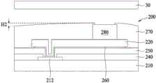
图2是例示本公开一些实施例的一封装半导体元件200。在一些实施例中,该封装半导体元件200包括一晶圆210,具有集成电路芯片,一第一绝缘层240,一第二绝缘层250,一导电薄膜260,一重布层220,一第三绝缘层270,以及一探测垫280。在一些实施例中,封装半导体元件200还包括至少一导电垫212,设置在晶圆210的一表面上。FIG. 2 is a packaged
在一些实施例中,第一绝缘层240设置在晶圆210上,导电垫212的至少一部分未被第一绝缘层240覆盖。在一些实施例中,保护层205覆盖导电垫212的侧壁及一顶表面的一部分。第二绝缘层250设置在第一绝缘层240上。导电薄膜260设置在第二绝缘层250及导电垫212上。重布层220设置在导电薄膜260上。第三绝缘层270设置在重布层220及第二绝缘层250上,其中探测垫280的一部分未被第三绝缘层270所覆盖。In some embodiments, the first insulating
比较图1和图2可以看出,在图1例示的实施例中,封装半导体元件100存在四个区域(虚线圆圈表示)可能发生底切现象,而在图2例示的实施例中,封装的半导体元件200仅有两个区域(虚线圆圈表示)可能发生底切现象。因此,与封装半导体元件100相比,本公开封装半导体元件200较不容易发生底切现象。此外,在图2中的探测垫280的底部没有底切,当需要减小探测垫280的尺寸以满足持续最小化芯片尺寸的要求时,探测垫280的尺寸不受底切的限制。1 and 2, it can be seen that in the embodiment illustrated in There are only two regions (indicated by dotted circles) of the
在一些实施例中,图2封装半导体元件200的一顶侧被晶粒结合薄膜30所覆盖。由于重布层220及探测垫280的存在,第三绝缘层270的轮廓于对应重布层220和探测垫280的区域显示出凸形(注意图2第三绝缘层270的凸形轮廓未按比例示出)。在一些实施例中,第三绝缘层270的下落高度(H2)可以被限制为小于3μm(微米)。相反地,因为图1的封装半导体元件100还包括一第四绝缘层190,不同于图2的封装半导体元件200。第四绝缘层190的下降高度(H1)增加至约5μm,其大于图2中的第三绝缘层270的下降高度(H2)。因此,封装的半导体元件200易于遭受诸如破裂、散热困难和低可靠性的问题。In some embodiments, a top side of the packaged
图3是例示本公开一些实施例的一封装半导体元件200'。比较图3与图2,封装半导体元件200'还包括设置在第一绝缘层240和芯片210之间的一保护层205,其中保护层20覆盖导电垫212的一部分。在一些实施例中,保护层205防止在制备芯片210结构的期间,芯片210被外部环境所污染。在一些实施例中,保护层205覆盖导电垫212的侧壁和顶表面的一部分,第一绝缘层240覆盖保护层205和导电垫212的顶表面的一部分。FIG. 3 is a packaged semiconductor device 200' illustrating some embodiments of the present disclosure. Comparing FIG. 3 with FIG. 2 , the packaged
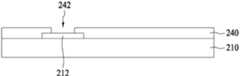
图4A至图4L例示说明本公开一些实施例的图2封装半导体元件的制造方法。参照图4A,提供一晶圆片210,并且在晶圆210的表面上至少形成一个导电垫212。在一些实施例中,导电垫212由铝制成,但本公开不限于此,且导电垫212可以由具有优异导电性的其他金属材料形成。4A-4L illustrate a method of fabricating the packaged semiconductor element of FIG. 2 according to some embodiments of the present disclosure. Referring to FIG. 4A , a
参照图4B,在晶圆210上形成一第一绝缘层240,第一绝缘层240包括一开口242,其暴露导电垫212的一部分。在一些实施例中,第一绝缘层240的材料主要是聚酰亚胺,但本公开不限于此,第一绝缘层240可以由其他具有优异电隔离的材料形成。在一些实施例中,第一绝缘层240是通过化学气相沉积(chemical vapor deposition,CVD)、等离子体辅助化学气相沉积镀膜(plasma enhanced chemical vapor deposition,PECVD)、旋涂或任何其他合适的工艺形成。Referring to FIG. 4B , a first insulating
参照图4C,第二绝缘层250形成在第一绝缘层240上,第二绝缘层250具有一开口252,开口252暴露导电垫212的一部分。在一些实施例中,第一绝缘层212覆盖导电垫212的侧壁和顶表面的一部分,第二绝缘层250覆盖第一绝缘层240和导电垫212的顶表面的一部分。第二绝缘层250的材料主要是聚酰亚胺,但本公开不限于此,第二绝缘层250可以由其他具有优异电隔离的材料形成。在一些实施例中,第二绝缘层250是通过化学气相沉积(CVD)、等离子体辅助化学气相沉积镀膜(PECVD)、旋涂或任何其他合适的工艺形成。Referring to FIG. 4C , a second insulating
在一些其他实施例中,第二绝缘层250和第一绝缘层240的特性可以略微不同;例如,第一绝缘层240和第二绝缘层250可以通过不同的制造者在不同的地方形成。例如,第一绝缘层240可以由上游(前端,frond-end)的制造商制造,第二绝缘层250可以由下游(后端,back-end)的制造商制造。因此,可能需要在不同温度下固化第一绝缘层240和第二绝缘层250。例如,第二绝缘层250可以在250℃(摄氏度)以下固化。在本实施例中,第一绝缘层240和第二绝缘层250是批次制造,但是本领域技术人员也可以选择同时制造第一绝缘层240和第二绝缘层250。In some other embodiments, the properties of the second insulating
参照图4D,在第二绝缘层250和导电垫212上形成一导电薄膜260,其中导电薄膜260物理接触导电垫212。在一些实施例中,导电薄膜260的材料是一钛/铜合金。Referring to FIG. 4D , a
参照图4E,在导电膜260上形成一第一图案化掩模20,并定义一第一区域255,其中区域255暴露导电薄膜260的一部分。在一些实施例中,第一图案化掩模20是一光刻胶层。Referring to FIG. 4E , a first patterned
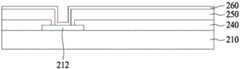
参照图4F,在第一区域255中形成一重布层220。在一些实施例中,使用导电薄膜260作为种子层将重布层220电镀在第一区域255上。在一些实施例中,重布层220的材料是铜。形成重布层220后,通过湿蚀刻工艺去除第一图案化掩模20,如图4G所示。Referring to FIG. 4F , a
参照图4H,在第二绝缘层250上形成一第二图案化掩模20'。在一些实施例中,第二图案化掩模20'覆盖侧壁和重布层220的一部分,并定义一第二区域275,其中第二区域275暴露重布层220的一部分,其中第二图案化掩模20'是一光刻胶层。Referring to FIG. 4H , a second patterned
参照图4I,在第二区域275上形成一金属块282。在一些实施例中,金属块282的材料与重布层220的材料相同,就是铜。Referring to FIG. 4I , a
参照图4J,在金属块282上形成金属保护层284。金属保护层284和金属块282形成探测垫280。在本实施例中,金属保护层284是镍金层,也就是金属保护层284是通过堆叠一镍(Ni)层和一金(Au)层所形成。Referring to FIG. 4J , a
参照图4K,通过湿蚀刻工艺移除第二图案化掩模20'。同时参照图4G和图4K,湿蚀刻工艺用于执行第一图案化掩模20和第二图案化掩模20'的移除。因为湿蚀刻工艺是等向性工艺,所以在重布层220的两端形成底切,如下图4K中虚线圆圈所示,为可能发生底切现象的区域。Referring to FIG. 4K, the second patterned mask 20' is removed through a wet etching process. 4G and 4K simultaneously, a wet etching process is used to perform the removal of the first patterned
参照图4L,一第三绝缘层270形成在重布层220和第二绝缘层250上,第三绝缘层270具有一开口272,以暴露金属保护层284。在一些实施例中,第三绝缘层270覆盖保护层284的侧壁及一顶表面的一部分。在一些实施例中,第三绝缘层270是通过化学气相沉积(CVD)、等离子体辅助化学气相沉积镀膜(PECVD)、旋涂或任何其他合适的工艺形成。Referring to FIG. 4L , a third
在一些实施例中,第三绝缘层270主要由聚酰亚胺制成。在图4A至图4L的制造过程之后,完成了图2封装半导体元件件200的制造。在封装半导体元件200完成之后,探针卡上的探针290可以通过开口272接触探测垫280。从以上可以看出,金属保护层(即镍金层)284设置在探测垫280的最上侧,因此,在探测垫280接触之后,探针290的尖端不保留任何的铜。随着探针290移动以接触晶圆210的切割道上的铝垫(类似于导电垫212),将不会发生铜转移;因此,可以有效地解决由铜引起的铝垫的氧化速率增加的问题。In some embodiments, the third insulating
图5A至图5D例示说明本公开一些实施例的一封装半导体元件的制造方法。参照图5A,封装半导体元件200的晶圆210被安装在具有一第一布线层312的一基板310上。第一布线层312的材料例如是铜。5A-5D illustrate a method of fabricating a packaged semiconductor device according to some embodiments of the present disclosure. Referring to FIG. 5A , the
在一些实施例中,在基底310上制造具有预定功能性的一电路。在一些实施例中,基板310包括多个导电线和多个电子元件,例如晶体管和二极管,并通过导线连接。在一些实施例中,基底310是一半导体基底。在一些实施例中,基底310是一中介层(interposer)或芯片。在一些实施例中,基底310是一硅基底。在一些实施例中,基底310包括一半导体材料,例如硅、锗、镓、砷、或其组合。在一些实施例中,基底310包括例如陶瓷、玻璃等材料。在一些实施例中,基底310是一玻璃基底。在一些实施例中,基底310是四边形、矩形、正方形、多边形或任何其他合适的形状。In some embodiments, a circuit with predetermined functionality is fabricated on the
参照图5B,一第四绝缘层320覆盖封装半导体元件200和第一布线层312。在本实施例中,第四绝缘层320用于固定封装的半导体元件200,主要由预浸料(prepreg)构成,预浸料是通过用绝缘纸、玻璃纤维布或其他纤维材料浸渍树脂而获得的粘合片。Referring to FIG. 5B , a fourth insulating
其次,参照图5B,在第四绝缘层320上形成一金属层330,金属层330的材料例如是铜。在一些实施例中,金属层330可以通过化学沉积技术形成。Next, referring to FIG. 5B , a
接着,参照图5C,通过激光钻孔在第四绝缘层320和金属层330中形成一第四开口322和多个第五开口324。第五开口324暴露第一布线层312的一部分。此外,第四开口322与第三开口272连通。在一些实施例中,第三开口272暴露封装半导体元件200的重布层220的一部分,暴露的部分可视为一接合垫222。Next, referring to FIG. 5C , a fourth opening 322 and a plurality of fifth openings 324 are formed in the fourth insulating
之后,参照图5D,形成具有一第一导电柱336和一第二导电柱334的一第二布线层332,其中第二导电柱334与接合垫222接触,第一导电柱336连接到第一布线层312。在一些实施例中,第二布线层332可以通过例如电镀一铜层,然后通过图案化工艺形成布线层的技术形成,此为本领域技术人员所熟知的。5D, a second wiring layer 332 having a first conductive post 336 and a second conductive post 334 is formed, wherein the second conductive post 334 is in contact with the bonding pad 222, and the first conductive post 336 is connected to the first conductive post 336.
本公开提供一封装半导体元件,包括一芯片,具有一导电垫;一第一绝缘层,设置在该芯片上;一第二绝缘层,设置在该第一绝缘层上;一导电薄膜,设置在该第二绝缘层上;一重布层,设置在该导电薄膜上;一探测垫,设置在该重布层上;以及一第三绝缘层,设置在该重布层及该第二绝缘层上。该第三绝缘层覆盖该探测垫的一部分,且该重布层和该探测垫之间的一区域中没有底切。当需要减小探测垫的尺寸以满足持续最小化芯片尺寸的要求时,探测垫的尺寸不受底切的限制。The present disclosure provides a packaged semiconductor element, including a chip with a conductive pad; a first insulating layer disposed on the chip; a second insulating layer disposed on the first insulating layer; a conductive film disposed on the chip on the second insulating layer; a redistribution layer on the conductive film; a detection pad on the redistribution layer; and a third insulating layer on the redistribution layer and the second insulating layer . The third insulating layer covers a portion of the probe pad, and there is no undercut in an area between the redistribution layer and the probe pad. The size of the probe pads is not limited by the undercut when it is necessary to reduce the size of the probe pads to meet the requirement of continuing to minimize the chip size.
本公开还提供一种封装半导体元件的制备方法。该制备方法包括:提供一芯片,具有一导电垫;形成一第一绝缘层在该芯片上,其中该第一绝缘层包括一第一开口,且该第一开口暴露该导电垫的一部分;形成一第二绝缘层在该第一绝缘层上;形成一导电薄膜在该第二绝缘层及该导电垫上;形成一第一图案化掩模在该第二绝缘层上,其中该第一图案化掩模定义一第一区域,该第一区域暴露该导电薄膜的一部分;形成一重布层在该第一区域中;形成一第二图案化掩模在该重布层上,其中该第二图案化掩模定义一第二区域,该第二区域暴露该重布层一部分;形成一探测垫在该第二区域中;以及形成一第三绝缘层在该重布层及该第二绝缘层上,其中该第三绝缘层包括一第二开口,且该第二开口暴露该探测垫一部分。The present disclosure also provides a preparation method of a packaged semiconductor element. The preparation method includes: providing a chip with a conductive pad; forming a first insulating layer on the chip, wherein the first insulating layer includes a first opening, and the first opening exposes a part of the conductive pad; forming A second insulating layer is formed on the first insulating layer; a conductive film is formed on the second insulating layer and the conductive pad; a first patterned mask is formed on the second insulating layer, wherein the first patterned The mask defines a first area, the first area exposes a portion of the conductive film; a redistribution layer is formed in the first area; a second patterned mask is formed on the redistribution layer, wherein the second pattern The chemical mask defines a second area that exposes a portion of the redistribution layer; a probe pad is formed in the second area; and a third insulating layer is formed on the redistribution layer and the second insulating layer , wherein the third insulating layer includes a second opening, and the second opening exposes a portion of the detection pad.
虽然已详述本公开及其优点,然而应理解可进行各种变化、取代与替代而不脱离权利要求所定义的本公开的精神与范围。例如,可用不同的方法实施上述的许多工艺,并且以其他工艺或其组合替代上述的许多工艺。Although the present disclosure and its advantages have been described in detail, it should be understood that various changes, substitutions and alterations can be made herein without departing from the spirit and scope of the disclosure as defined by the appended claims. For example, many of the processes described above may be performed in different ways and replaced by other processes or combinations thereof.
再者,本公开的范围并不受限于说明书中所述的工艺、机械、制造、物质组成物、手段、方法与步骤的特定实施例。该领域的技术人士可自本公开的公开内容理解可根据本公开而使用与本文所述的对应实施例具有相同功能或是达到实质相同结果的现存或是未来发展的工艺、机械、制造、物质组成物、手段、方法、或步骤。据此,这些工艺、机械、制造、物质组成物、手段、方法、或步骤包含于本公开的权利要求内。Furthermore, the scope of the present disclosure is not limited to the specific embodiments of the process, machinery, manufacture, compositions of matter, means, methods and steps described in the specification. Those skilled in the art can understand from the disclosure of the present disclosure that existing or future developed processes, machines, manufactures, materials that have the same function or achieve substantially the same results as the corresponding embodiments described herein can be used in accordance with the present disclosure. A composition, means, method, or step. Accordingly, such processes, machines, manufacture, compositions of matter, means, methods, or steps are included within the claims of the present disclosure.
Claims (20)
Translated fromChineseApplications Claiming Priority (2)
| Application Number | Priority Date | Filing Date | Title |
|---|---|---|---|
| US16/046,100 | 2018-07-26 | ||
| US16/046,100US20200035629A1 (en) | 2018-07-26 | 2018-07-26 | Packaged semiconductor device and method for preparing the same |
Publications (1)
| Publication Number | Publication Date |
|---|---|
| CN110767621Atrue CN110767621A (en) | 2020-02-07 |
Family
ID=69178668
Family Applications (1)
| Application Number | Title | Priority Date | Filing Date |
|---|---|---|---|
| CN201811209108.6APendingCN110767621A (en) | 2018-07-26 | 2018-10-17 | Packaged semiconductor element and method of making the same |
Country Status (3)
| Country | Link |
|---|---|
| US (1) | US20200035629A1 (en) |
| CN (1) | CN110767621A (en) |
| TW (1) | TWI680546B (en) |
Families Citing this family (5)
| Publication number | Priority date | Publication date | Assignee | Title |
|---|---|---|---|---|
| US12015002B2 (en) | 2021-08-30 | 2024-06-18 | Taiwan Semiconductor Manufacturing Company, Ltd. | Chip structure and method for forming the same |
| US11688708B2 (en) | 2021-08-30 | 2023-06-27 | Taiwan Semiconductor Manufacturing Company, Ltd. | Chip structure and method for forming the same |
| US12159852B2 (en)* | 2022-04-27 | 2024-12-03 | Nanya Technology Corporation | Semiconductor device structure with composite bottle-shaped through silicon via and method for preparing the same |
| TWI835336B (en)* | 2022-10-11 | 2024-03-11 | 群創光電股份有限公司 | Electronic device and manufacturing method thereof |
| TWI861796B (en)* | 2023-03-31 | 2024-11-11 | 矽品精密工業股份有限公司 | Electronic package and electronic structure thereof |
Citations (6)
| Publication number | Priority date | Publication date | Assignee | Title |
|---|---|---|---|---|
| US20070164279A1 (en)* | 2005-12-05 | 2007-07-19 | Megica Corporation | Semiconductor chip |
| US20120032340A1 (en)* | 2010-08-06 | 2012-02-09 | Stats Chippac, Ltd. | Semiconductor Die and Method of Forming FO-WLCSP Vertical Interconnect Using TSV and TMV |
| US20120091582A1 (en)* | 2006-12-20 | 2012-04-19 | Tessera, Inc. | Microelectronic assemblies having compliancy and methods therefor |
| CN104051429A (en)* | 2013-03-11 | 2014-09-17 | 台湾积体电路制造股份有限公司 | Methods and apparatus for wafer level packaging |
| CN107437536A (en)* | 2016-05-26 | 2017-12-05 | 台湾积体电路制造股份有限公司 | Sensor package |
| US20180166405A1 (en)* | 2016-12-13 | 2018-06-14 | Taiwan Semiconductor Manufacturing Co. Ltd. | Structure and formation method of chip package with antenna element |
- 2018
- 2018-07-26USUS16/046,100patent/US20200035629A1/ennot_activeAbandoned
- 2018-09-05TWTW107131105Apatent/TWI680546B/enactive
- 2018-10-17CNCN201811209108.6Apatent/CN110767621A/enactivePending
Patent Citations (6)
| Publication number | Priority date | Publication date | Assignee | Title |
|---|---|---|---|---|
| US20070164279A1 (en)* | 2005-12-05 | 2007-07-19 | Megica Corporation | Semiconductor chip |
| US20120091582A1 (en)* | 2006-12-20 | 2012-04-19 | Tessera, Inc. | Microelectronic assemblies having compliancy and methods therefor |
| US20120032340A1 (en)* | 2010-08-06 | 2012-02-09 | Stats Chippac, Ltd. | Semiconductor Die and Method of Forming FO-WLCSP Vertical Interconnect Using TSV and TMV |
| CN104051429A (en)* | 2013-03-11 | 2014-09-17 | 台湾积体电路制造股份有限公司 | Methods and apparatus for wafer level packaging |
| CN107437536A (en)* | 2016-05-26 | 2017-12-05 | 台湾积体电路制造股份有限公司 | Sensor package |
| US20180166405A1 (en)* | 2016-12-13 | 2018-06-14 | Taiwan Semiconductor Manufacturing Co. Ltd. | Structure and formation method of chip package with antenna element |
Also Published As
| Publication number | Publication date |
|---|---|
| US20200035629A1 (en) | 2020-01-30 |
| TWI680546B (en) | 2019-12-21 |
| TW202008520A (en) | 2020-02-16 |
Similar Documents
| Publication | Publication Date | Title |
|---|---|---|
| CN110767621A (en) | Packaged semiconductor element and method of making the same | |
| CN110838473B (en) | Semiconductor package and manufacturing method thereof | |
| TWI512930B (en) | Chip package and method for forming the same | |
| CN104576584B (en) | Semiconductor devices and its manufacture method | |
| TWI582913B (en) | Semiconductor package and method of manufacture | |
| CN113140519A (en) | Wafer level package employing molded interposer | |
| US11923318B2 (en) | Method of manufacturing semiconductor package | |
| CN105374778B (en) | Chip package and method for manufacturing the same | |
| KR20200134377A (en) | Semiconductor Package | |
| US11764168B2 (en) | Chip package structure with anchor structure and method for forming the same | |
| US12068273B2 (en) | Package | |
| CN108022966A (en) | Semiconductor chip and semiconductor package | |
| CN115101482A (en) | Semiconductor packaging structure and forming method thereof | |
| US20160355393A1 (en) | Chip package and manufacturing method thereof | |
| CN106206460B (en) | Chip package and method for manufacturing the same | |
| US10461060B2 (en) | Structure and formation method of chip package with redistribution layers | |
| US20180204814A1 (en) | Method for preparing a semiconductor package | |
| TWI738923B (en) | Semiconductor structure and manufacturing method thereof | |
| CN106206557A (en) | Silicon Interposer | |
| US20240282712A1 (en) | Semiconductor device and method of manufacturing the same | |
| CN110634831B (en) | Semiconductor device package and manufacturing method thereof | |
| KR101059625B1 (en) | Wafer level chip scale package and its manufacturing method | |
| KR100969444B1 (en) | Wafer level chip scale package having patterned resin seal and manufacturing method thereof | |
| CN223108878U (en) | Semiconductor Package | |
| TWI653726B (en) | Semiconductor substrate and manufacturing method thereof |
Legal Events
| Date | Code | Title | Description |
|---|---|---|---|
| PB01 | Publication | ||
| PB01 | Publication | ||
| SE01 | Entry into force of request for substantive examination | ||
| SE01 | Entry into force of request for substantive examination | ||
| WD01 | Invention patent application deemed withdrawn after publication | ||
| WD01 | Invention patent application deemed withdrawn after publication | Application publication date:20200207 |