CN110753962A - memory circuit - Google Patents
memory circuitDownload PDFInfo
- Publication number
- CN110753962A CN110753962ACN201880039786.4ACN201880039786ACN110753962ACN 110753962 ACN110753962 ACN 110753962ACN 201880039786 ACN201880039786 ACN 201880039786ACN 110753962 ACN110753962 ACN 110753962A
- Authority
- CN
- China
- Prior art keywords
- memory
- space
- rows
- electrically coupled
- alternating
- Prior art date
- Legal status (The legal status is an assumption and is not a legal conclusion. Google has not performed a legal analysis and makes no representation as to the accuracy of the status listed.)
- Pending
Links
- 238000003491arrayMethods0.000claimsabstractdescription69
- 239000003990capacitorSubstances0.000claimsabstractdescription39
- 239000004020conductorSubstances0.000claimsdescription13
- 239000000463materialSubstances0.000description42
- 239000000758substrateSubstances0.000description10
- 230000010287polarizationEffects0.000description7
- 238000010276constructionMethods0.000description6
- 230000005669field effectEffects0.000description5
- 239000012212insulatorSubstances0.000description5
- VYPSYNLAJGMNEJ-UHFFFAOYSA-NSilicium dioxideChemical compoundO=[Si]=OVYPSYNLAJGMNEJ-UHFFFAOYSA-N0.000description4
- 239000011810insulating materialSubstances0.000description4
- 239000000203mixtureSubstances0.000description4
- 230000002441reversible effectEffects0.000description3
- 239000002019doping agentSubstances0.000description2
- 230000005611electricityEffects0.000description2
- 239000012535impuritySubstances0.000description2
- 230000014759maintenance of locationEffects0.000description2
- 238000004519manufacturing processMethods0.000description2
- 239000002184metalSubstances0.000description2
- 229910052751metalInorganic materials0.000description2
- 239000007769metal materialSubstances0.000description2
- 238000000034methodMethods0.000description2
- 239000004065semiconductorSubstances0.000description2
- 235000012239silicon dioxideNutrition0.000description2
- 239000000377silicon dioxideSubstances0.000description2
- 229910052581Si3N4Inorganic materials0.000description1
- 229910045601alloyInorganic materials0.000description1
- 239000000956alloySubstances0.000description1
- 238000000231atomic layer depositionMethods0.000description1
- 229910002056binary alloyInorganic materials0.000description1
- 239000003795chemical substances by applicationSubstances0.000description1
- 238000005229chemical vapour depositionMethods0.000description1
- 229910052681coesiteInorganic materials0.000description1
- 230000008878couplingEffects0.000description1
- 238000010168coupling processMethods0.000description1
- 238000005859coupling reactionMethods0.000description1
- 229910052906cristobaliteInorganic materials0.000description1
- 238000013500data storageMethods0.000description1
- 238000010586diagramMethods0.000description1
- 238000009792diffusion processMethods0.000description1
- 230000005684electric fieldEffects0.000description1
- 239000012777electrically insulating materialSubstances0.000description1
- 230000002708enhancing effectEffects0.000description1
- 230000006870functionEffects0.000description1
- 238000005468ion implantationMethods0.000description1
- 150000002736metal compoundsChemical class0.000description1
- 150000002739metalsChemical class0.000description1
- 229910021421monocrystalline siliconInorganic materials0.000description1
- 230000002093peripheral effectEffects0.000description1
- 238000005240physical vapour depositionMethods0.000description1
- HQVNEWCFYHHQES-UHFFFAOYSA-Nsilicon nitrideChemical compoundN12[Si]34N5[Si]62N3[Si]51N64HQVNEWCFYHHQES-UHFFFAOYSA-N0.000description1
- 229910052682stishoviteInorganic materials0.000description1
- 238000003860storageMethods0.000description1
- 229910052905tridymiteInorganic materials0.000description1
Images


Classifications
- H—ELECTRICITY
- H10—SEMICONDUCTOR DEVICES; ELECTRIC SOLID-STATE DEVICES NOT OTHERWISE PROVIDED FOR
- H10B—ELECTRONIC MEMORY DEVICES
- H10B12/00—Dynamic random access memory [DRAM] devices
- G—PHYSICS
- G11—INFORMATION STORAGE
- G11C—STATIC STORES
- G11C5/00—Details of stores covered by group G11C11/00
- G11C5/06—Arrangements for interconnecting storage elements electrically, e.g. by wiring
- G11C5/063—Voltage and signal distribution in integrated semi-conductor memory access lines, e.g. word-line, bit-line, cross-over resistance, propagation delay
- G—PHYSICS
- G11—INFORMATION STORAGE
- G11C—STATIC STORES
- G11C11/00—Digital stores characterised by the use of particular electric or magnetic storage elements; Storage elements therefor
- G11C11/21—Digital stores characterised by the use of particular electric or magnetic storage elements; Storage elements therefor using electric elements
- G11C11/34—Digital stores characterised by the use of particular electric or magnetic storage elements; Storage elements therefor using electric elements using semiconductor devices
- G11C11/40—Digital stores characterised by the use of particular electric or magnetic storage elements; Storage elements therefor using electric elements using semiconductor devices using transistors
- G11C11/401—Digital stores characterised by the use of particular electric or magnetic storage elements; Storage elements therefor using electric elements using semiconductor devices using transistors forming cells needing refreshing or charge regeneration, i.e. dynamic cells
- G11C11/4063—Auxiliary circuits, e.g. for addressing, decoding, driving, writing, sensing or timing
- G11C11/407—Auxiliary circuits, e.g. for addressing, decoding, driving, writing, sensing or timing for memory cells of the field-effect type
- G11C11/408—Address circuits
- G11C11/4085—Word line control circuits, e.g. word line drivers, - boosters, - pull-up, - pull-down, - precharge
- G—PHYSICS
- G11—INFORMATION STORAGE
- G11C—STATIC STORES
- G11C5/00—Details of stores covered by group G11C11/00
- G11C5/02—Disposition of storage elements, e.g. in the form of a matrix array
- G11C5/025—Geometric lay-out considerations of storage- and peripheral-blocks in a semiconductor storage device
- H—ELECTRICITY
- H10—SEMICONDUCTOR DEVICES; ELECTRIC SOLID-STATE DEVICES NOT OTHERWISE PROVIDED FOR
- H10D—INORGANIC ELECTRIC SEMICONDUCTOR DEVICES
- H10D1/00—Resistors, capacitors or inductors
- H10D1/60—Capacitors
- H10D1/68—Capacitors having no potential barriers
- H10D1/692—Electrodes
- H10D1/711—Electrodes having non-planar surfaces, e.g. formed by texturisation
- H10D1/716—Electrodes having non-planar surfaces, e.g. formed by texturisation having vertical extensions
- H—ELECTRICITY
- H10—SEMICONDUCTOR DEVICES; ELECTRIC SOLID-STATE DEVICES NOT OTHERWISE PROVIDED FOR
- H10D—INORGANIC ELECTRIC SEMICONDUCTOR DEVICES
- H10D30/00—Field-effect transistors [FET]
- H10D30/60—Insulated-gate field-effect transistors [IGFET]
- H10D30/63—Vertical IGFETs
- G—PHYSICS
- G11—INFORMATION STORAGE
- G11C—STATIC STORES
- G11C11/00—Digital stores characterised by the use of particular electric or magnetic storage elements; Storage elements therefor
- G11C11/21—Digital stores characterised by the use of particular electric or magnetic storage elements; Storage elements therefor using electric elements
- G11C11/34—Digital stores characterised by the use of particular electric or magnetic storage elements; Storage elements therefor using electric elements using semiconductor devices
- G11C11/40—Digital stores characterised by the use of particular electric or magnetic storage elements; Storage elements therefor using electric elements using semiconductor devices using transistors
- G11C11/401—Digital stores characterised by the use of particular electric or magnetic storage elements; Storage elements therefor using electric elements using semiconductor devices using transistors forming cells needing refreshing or charge regeneration, i.e. dynamic cells
- G11C11/4063—Auxiliary circuits, e.g. for addressing, decoding, driving, writing, sensing or timing
- G11C11/407—Auxiliary circuits, e.g. for addressing, decoding, driving, writing, sensing or timing for memory cells of the field-effect type
- G11C11/409—Read-write [R-W] circuits
- G11C11/4097—Bit-line organisation, e.g. bit-line layout, folded bit lines
Landscapes
- Engineering & Computer Science (AREA)
- Microelectronics & Electronic Packaging (AREA)
- Computer Hardware Design (AREA)
- Semiconductor Memories (AREA)
Abstract
Translated fromChinese
Description
Translated fromChinese技术领域technical field
本文公开的实施例涉及存储器电路。Embodiments disclosed herein relate to memory circuits.
背景技术Background technique
存储器是一种集路且在计算机系统中用于存储数据。存储器可制造成个别存储器单元的一或多个阵列。可使用数字线(其也可称作位线、数据线、感测线)和存取线(其也可称作字线)对存储器单元进行写入或从存储器单元进行读取。数字线可使存储器单元沿着阵列的列以导电方式互连,并且存取线可使存储器单元沿着阵列的行以导电方式互连。可通过数字线和存取线的组合对每个存储器单元进行唯一地寻址。Memory is a collection of circuits and is used in computer systems to store data. Memory can be fabricated as one or more arrays of individual memory cells. Memory cells may be written to or read from memory cells using digit lines (which may also be referred to as bit lines, data lines, sense lines) and access lines (which may also be referred to as word lines). Digit lines may electrically interconnect memory cells along the columns of the array, and access lines may electrically interconnect memory cells along the rows of the array. Each memory cell is uniquely addressable by a combination of digit lines and access lines.
存储器单元可以是易失性的、半易失性的或非易失性的。非易失性存储器单元可在不通电的情况下将数据存储很长一段时间。非易失性存储器通常被指定为具有至少约10年保持时间的存储器。易失性存储器会消散,且因此经刷新/重写以维持数据存储。易失性存储器可具有数毫秒或更短的保留时间。无论如何,存储器单元被配置成以至少两个不同可选状态保留或存储存储器。在二进制系统中,状态被认为是“0”或“1”。在其它系统中,至少一些个别存储器单元可被配置成存储多于两个位或状态的信息。Memory cells can be volatile, semi-volatile or non-volatile. Non-volatile memory cells can store data for long periods of time without powering up. Non-volatile memory is typically specified as memory with a retention time of at least about 10 years. Volatile memory is dissipated and thus refreshed/rewritten to maintain data storage. Volatile memory can have retention times of milliseconds or less. Regardless, the memory unit is configured to retain or store memory in at least two different selectable states. In the binary system, states are considered to be "0" or "1". In other systems, at least some of the individual memory cells may be configured to store more than two bits or states of information.
电容器是可用于存储器单元中的一种类型的电子组件。电容器具有由电绝缘材料分离的两个电导体。能量如电场可以静电方式存储在此类材料内。取决于绝缘材料的组成,所述存储的场将是易失性的或非易失性的。举例来说,仅包含SiO2的电容器绝缘材料将是易失性的。一种类型的非易失性电容器是铁电电容器,所述铁电电容器具有铁电材料作为绝缘材料的至少部分。铁电材料的特征为具有两个稳定极化状态且由此可包括电容器和/或存储器单元的可编程材料。铁电材料的极化状态可通过施加合适的编程电压来改变,且在移除编程电压之后保持住(至少持续一时间)。每个极化状态具有彼此不同的存储电荷的电容,且理想地可用于在不颠倒极化状态的情况下写入(即,存储)和读取(即,确定)存储器状态,直到期望颠倒此类极化状态为止。不太合意地,在具有铁电电容器的某个存储器中,读取存储器状态的行为可能会颠倒极化。因此,在确定极化状态后,进行对存储器单元的重写以紧接在其确定之后将存储器单元置于预读取状态中。无论如何,由于形成电容器的部分的铁电材料的双稳态特性,因此并入有铁电电容器的存储器单元理想地是非易失性的。Capacitors are one type of electronic component that can be used in memory cells. A capacitor has two electrical conductors separated by an electrically insulating material. Energy such as electric fields can be electrostatically stored within such materials. Depending on the composition of the insulating material, the stored field will be volatile or non-volatile. For example, a capacitor insulating material containing onlySiO2 would be volatile. One type of nonvolatile capacitor is a ferroelectric capacitor, which has a ferroelectric material as at least part of the insulating material. Ferroelectric materials are characterized as programmable materials that have two stable polarization states and thus can include capacitors and/or memory cells. The polarization state of the ferroelectric material can be changed by applying an appropriate programming voltage, and is maintained (for at least a period of time) after the programming voltage is removed. Each polarization state has a different capacitance of stored charge from each other, and ideally can be used to write (ie, store) and read (ie, determine) a memory state without reversing the polarization state, until it is desired to reverse this up to the polarization-like state. Less desirable, in a memory with ferroelectric capacitors, the act of reading the memory state may reverse the polarization. Therefore, after the polarization state is determined, a rewrite of the memory cell is performed to place the memory cell in a pre-read state immediately after its determination. Regardless, memory cells incorporating ferroelectric capacitors are ideally non-volatile due to the bistable nature of the ferroelectric materials that form part of the capacitor.
场效应晶体管是可用于存储器单元的另一类型的电子组件。这些晶体管包括一对源极/漏极区,所述一对源极/漏极区在其间具有半导体沟道区。导电栅极邻近于沟道区且通过薄的栅极绝缘体与沟道区分离。向栅极施加合适的电压允许电流通过沟道区从源极/漏极区中的一个区流动到另一个区。当从栅极移除电压时,大大地防止了电流流动通过沟道区。场效应晶体管还可包含额外结构,例如,作为栅极绝缘体与导电栅极之间的栅极构造的部分的可逆可编程电荷存储区。场效应晶体管可以是铁电的,其中栅极构造的至少某一部分(例如,栅极绝缘体)包括铁电材料。晶体管中的铁电材料的两个不同极化状态的特征可在于晶体管的不同阈值电压(Vt)或在于选定操作电压的不同沟道导电性。Field effect transistors are another type of electronic component that can be used in memory cells. These transistors include a pair of source/drain regions with a semiconductor channel region therebetween. A conductive gate is adjacent to and separated from the channel region by a thin gate insulator. Applying an appropriate voltage to the gate allows current to flow from one of the source/drain regions through the channel region to the other. When the voltage is removed from the gate, current flow through the channel region is greatly prevented. Field effect transistors may also include additional structures, such as reversible programmable charge storage regions that are part of the gate construction between the gate insulator and the conductive gate. Field effect transistors may be ferroelectric, wherein at least some portion of the gate construction (eg, the gate insulator) includes a ferroelectric material. The two different polarization states of the ferroelectric material in the transistor may be characterized by different threshold voltages (Vt ) of the transistor or by different channel conductivities at the selected operating voltage.
一种类型的易失性存储器为动态随机存取存储器(DRAM)。其用于现代计算架构中,且与其它类型的存储器相比可提供结构简单、成本低和速度快的优点。当前,DRAM通常具有个别存储器单元具有与一个场效应晶体管组合的一个电容器(所谓的1T-1C存储器单元),其中所述电容器耦合到所述晶体管的源极/漏极区中的一者。当前1T-1C配置的可扩展性的一个局限性在于,难以将具有足够高电容的电容器并入到高集成度的架构中。One type of volatile memory is dynamic random access memory (DRAM). It is used in modern computing architectures and offers the advantages of simplicity, low cost and speed compared to other types of memory. Currently, DRAMs typically have individual memory cells with one capacitor in combination with one field effect transistor (so-called 1T-1C memory cells), where the capacitor is coupled to one of the transistor's source/drain regions. One limitation of the scalability of current 1T-1C configurations is that it is difficult to incorporate capacitors with sufficiently high capacitance into highly integrated architectures.
附图说明Description of drawings
图1是2T-1C存储器单元的示意图。Figure 1 is a schematic diagram of a 2T-1C memory cell.
图2是根据本发明的实施例的存储器电路的图解混合示意图和部分构造视图。2 is a diagrammatic hybrid schematic and partial construction view of a memory circuit in accordance with an embodiment of the present invention.
图3是穿过图2中的线3-3截取的混合构造和部分示意性横截面图。FIG. 3 is a partial schematic cross-sectional view of the hybrid configuration taken through line 3-3 in FIG. 2 .
图4是穿过图2中的线4-4截取的分段横截面图。FIG. 4 is a segmented cross-sectional view taken through line 4 - 4 in FIG. 2 .
图5是图2和如图4所示的一部分的图解放大俯视图。FIG. 5 is a diagrammatic enlarged top view of a portion shown in FIGS. 2 and 4 .
图6是穿过图5中的线6-6截取的横截面图。FIG. 6 is a cross-sectional view taken through line 6 - 6 in FIG. 5 .
图7是穿过图5中的线7-7截取的横截面图。FIG. 7 is a cross-sectional view taken through line 7-7 in FIG. 5. FIG.
图8是穿过图5中的线8-8截取的横截面图。FIG. 8 is a cross-sectional view taken through line 8 - 8 in FIG. 5 .
图9是穿过图5中的线9-9截取的横截面图。FIG. 9 is a cross-sectional view taken through line 9 - 9 in FIG. 5 .
图10是存储器电路的图解混合示意图和部分构造视图。10 is a diagrammatic hybrid schematic and partial construction view of a memory circuit.
图11是图10的一部分的图解放大俯视图。FIG. 11 is a diagrammatic enlarged top view of a portion of FIG. 10 .
图12是穿过图11中的线12-12截取的横截面图。FIG. 12 is a cross-sectional view taken through line 12 - 12 in FIG. 11 .
具体实施方式Detailed ways
本发明的实施例包含包括个别地具有至少两个晶体管和至少一个电容器的存储器单元的存储器电路。在一些此类实施例中,个别存储器单元具有不超过总共两个晶体管和不超过总共一个电容器,且其通常由所属领域的技术人员称为两晶体管-一电容器(2T-1C)存储器单元且如图1示意性展示。实例2T-1C存储器单元MC具有两个晶体管T1和T2以及电容器CAP。T1的源极/漏极区与电容器CAP的第一节点连接,且T1的另一源极/漏极区与第一比较数字线(例如,DL-T)连接。T1的栅极与存取线AL(即,字线)连接。T2的源极/漏极区与电容器CAP的第二节点连接,且T2的另一源极/漏极区与第二比较数字线(例如,DL-C)连接。T2的栅极与存取线AL连接。比较数字线DL-T和DL-C延伸到电路4,所述电路比较两者的电性质(例如,电压)以确认存储器单元MC的存储器状态。图1的2T-1C配置可用于DRAM和/或其它类型的存储器中。Embodiments of the invention include memory circuits including memory cells individually having at least two transistors and at least one capacitor. In some such embodiments, individual memory cells have no more than two transistors in total and no more than one capacitor in total, and are commonly referred to by those skilled in the art as two-transistor-one-capacitor (2T-1C) memory cells and as Figure 1 shows schematically. Example 2T-1C memory cell MC has two transistors T1 and T2 and a capacitor CAP. The source/drain region of T1 is connected to the first node of the capacitor CAP, and the other source/drain region of T1 is connected to the first comparison digit line (eg, DL-T). The gate of T1 is connected to the access line AL (ie, the word line). The source/drain region of T2 is connected to the second node of the capacitor CAP, and the other source/drain region of T2 is connected to the second comparison digit line (eg, DL-C). The gate of T2 is connected to the access line AL. The comparison digit lines DL-T and DL-C extend to
图2-9展示包括2T-1C存储器单元12的存储器电路,但预期包括个别地具有多于总共两个晶体管和/或多于总共一个电容器的存储器单元的存储器电路,不管是现有还是有待开发的。实例存储器电路包括在基底衬底15上方的衬底、构造或装置10,其可包含导电/导体/传导(即,在本文中,传导电)、半导电/半导体半传导或绝缘/绝缘体/绝缘(即,在本文中,电绝缘)材料中的任何一或多者。各种材料已经形成于基底衬底15上。材料可在图2-9所描绘材料的旁边、竖向内侧或竖向向外。举例来说,集成电路的其它部分制造或完全制造的组件可提供于基底衬底15上方、周围或内部某处。用于操作存储器单元阵列内的组件的控制和/或其它外围电路也可制造,且可或可不完全或部分地在阵列或子阵列内。此外,也可相对彼此独立地、先后地(in tandem)或以其它方式制造和操作多个子阵列。如此文件中所使用,“子阵列”也可被视为阵列。实例基底衬底15可包括适当掺杂的半导体材料(例如,单晶硅)。2-9 show memory circuits including 2T-
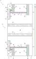
根据本发明的构造10和存储器电路包括其间具有横向空间250的一对紧邻的存储器阵列300和400(例如,2T-1C存储器阵列)。关于存储器阵列300和400,提及“紧邻”意指其间不存在其它存储器阵列。关于其它区、特征或组件,提及“紧邻”也意指其间不存在其它此类区、此类特征或此类组件。存储器阵列300和400展示为包括相应周边轮廓305和405,其作为实例被展示为相应相同大小的正方形。当然可使用替代的大小和形状,且实例阵列300和400不需要相对于彼此具有相同的大小和/或形状。另外,周长轮廓305和405可以不由物理特征界定。相反,作为实例,其可包含在存储器阵列的边缘处的狭窄界面区/部分,其中个别存储器单元的重复布置停止且空间250开始,而与空间250在存储器阵列300和/或400内不具有相同的重复组件布置无关。图2中仅展示两个并排的存储器阵列300和400,但很可能会在存储器阵列300和400的左、右以及上方和下方提供数十个、数百个、数千个等(未展示)。空间250展示为具有横向宽阔区255和265,其可相对于彼此具有相同的尺寸或可彼此具有不同的尺寸。空间250展示为四边形形状,但可使用任何替代形状。
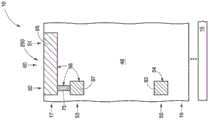
存储器阵列300和400个别地包括存储器单元12,所述存储器单元个别地包括上部竖向延伸晶体管TU(图3和4)和下部竖向延伸晶体管TL,且在其间具有竖向电容器14。
存储器阵列300和400包括在上部数字线层级17处的第一比较数字线DL-C的列16,其在上部竖向延伸晶体管TU的列18上方(在一个实施例中,正上方)且电耦合到(在一个实施例中,直接电耦合到)所述列。存储器阵列300和400包括在下部数字线层级19处的第二比较数字线DL-T的列20,其在下部竖向延伸晶体管TL的列22下方(在一个实施例中,正下方)且电耦合到(在一个实施例中,直接电耦合到)所述列。实例晶体管TU和TL个别地包括上部源极/漏极区26、下部源极/漏极区28以及在其间的竖向沟道区30。晶体管栅极32展示为在沟道区30的相对侧上,且由栅极绝缘体34与其隔开。源极/漏极区26、28可被重掺杂有增强导电性的杂质以导电,例如具有至少为1020个原子/cm3的掺杂剂浓度。沟道区30可适当地掺杂有可能具有与区26和28中的掺杂剂相反的导电类型的导电性修改杂质,例如达到小于或等于约1016个原子/cm3的沟道掺杂剂浓度。本文的导电组件、特征、区和材料可包括导电掺杂半导电材料和/或金属材料中的一或多者、基本上由其组成和/或由其组成。
在一个实施例中且如图所示,上部竖向延伸晶体管TU是竖直的或在竖直的10°之内,且下部竖向延伸晶体管TL是竖直的或在竖直的10°之内。在一个此类实施例中且如图所示,个别存储单元12中的上部竖向延伸晶体管和下部竖向延伸晶体管共享共同的直线轴线35,在操作中,电流沿着所述直线轴线流过相应的上部竖向延伸晶体管和下部竖向延伸晶体管的沟道30。在一个实施例中且如图所示,下部晶体管TL的下部源极/漏极区28直接电耦合到比较数字线DL-T,且在一个实施例中,上部晶体管TU的上部源极/漏极区26直接电耦合到比较数字线线DL-C。DL-T和DL-C的竖向位置可颠倒。In one embodiment and as shown, the upper vertically extending transistor TU is vertical or within 10° of vertical and the lower vertically extending transistor TL is vertical or within 10° of vertical Inside. In one such embodiment and as shown, the upper and lower vertically extending transistors in
电容器14包括上部电极38、下部电极40以及在其间的电容器绝缘体41。下部电容器电极40展示为导电柱,且上部电容器电极38展示为环绕下部电极柱40的上部部分的面向下的容器。这种关系可颠倒,例如,下部电容器电极是面向上的容器,且上部电容器电极是向下突出的柱。可使用任何替代的电容器构造,例如,不包括类似容器的结构和/或不包括柱。
存储器阵列300和400共享第一交替行50、51和第二交替行60。第二交替行60个别地在紧邻的第一交替行50和51之间。第一交替行50、51和第二交替行60中的个别者具有位于下部存取线层级55中的下部存取线54的上方的上部存取线层级53中的上部存取线52。个别上部存取线52和下部存取线54在图5中至少为了此图清楚起见而展示为至少彼此横向偏移。线52和54可能并不如此偏移,且彼此之间无需具有相同的大小和形状。
个别第一交替行50、51和个别第二交替行60中的上部存取线52和下部存取线54通过导体互连件58直接电耦合在一起。此类互连件包括在上部数字线层级17内的水平延伸部分62,其在个别的第一交替行50、51或第二交替行60中的上部存取线52和下部存取线54两者的正上方。存储器阵列300和400中的个别第一交替行50跨越空间250直接彼此耦合。存储器阵列300和400中的个别第一交替行51跨越空间250直接彼此电耦合。存储器阵列300和400中的个别第二交替行60不跨越空间250直接彼此电耦合。The
第一交替行50、51中的交替行50中的下部存取线54从存储器阵列300、400中的一者跨越空间250延伸到存储器阵列300、400中的另一者。第一交替行50、51中的交替行51中的下部存取线54不从存储阵列300、400中的一者跨越空间250延伸到存储阵列300、400中的另一者。第一交替行50、51中的交替行51个别地在第一交替行50、51中的交替行50的紧邻者之间。存储器阵列300、400中的交替的其它第一交替行51中的个别者通过导电互连件66跨越空间250直接彼此电耦合。此类互连件包含在上部数字线层级17中在空间250中的一个水平细长部分65和在上部存取线层级53中在空间250中的另一水平细长部分67。空间250中的此类另一水平细长部分67在第一交替行50、51中的交替行50中的紧邻行中的下部存取线54正上方。个别导体互连间58和导电互连件66可首尾相连和/或以其它方式彼此成一体。The
在一个实施例中,多个导电通孔95在第一交替行50、51中的两个紧邻交替行50、51之间横向地在空间250内从上部数字线层级17延伸到下部数字线层级19(在一个实施例中,从层级17上方延伸到层级19下方)。In one embodiment, a plurality of
实例绝缘材料48(例如,二氧化硅和/或氮化硅)展示为囊封上文所描述的各种特征和组件。Example insulating materials 48 (eg, silicon dioxide and/or silicon nitride) are shown to encapsulate the various features and components described above.
在一些实施例中,且除非独立于上文所描述的一或多个方面另有陈述,否则存储器电路包括一对紧邻的存储器阵列(例如,300和400),在其间横向地具有空间(例如,250)。然而,可使用如图所示和/或本文中相对于其它实施例所描述的任何其它属性或方面。存储器阵列个别地包括存储器单元(例如,12),所述存储器单元个别地具有上部竖向延伸晶体管(例如,TU)和下部竖向延伸晶体管(例如,TL)以及在其间的竖向电容器(例如,14)。存储器阵列包括个别行(例如,行50、51、60中的任何两者或更多者),其(a)具有在下部存取线(例如,54)上方且直接电耦合到所述下部存取线的上部存取线(例如,52),且(b)跨越所述空间直接彼此电耦合。所述行中的一者(例如,行50中的任一者)中的下部存取线从所述存储器阵列中的一者跨越所述空间延伸到所述存储器阵列中的另一者。所述行中的另一者(例如,行51中的任一者)包括导电互连件(例如,66),所述导电互连件包含在所述空间内从另一行横向偏移的水平延伸部分(例如,67)。In some embodiments, and unless otherwise stated independently of one or more aspects described above, a memory circuit includes a pair of immediately adjacent memory arrays (eg, 300 and 400 ) with space laterally therebetween (eg, , 250). However, any other attributes or aspects shown in the figures and/or described herein with respect to other embodiments may be used. The memory arrays individually include memory cells (eg, 12 ) that individually have upper vertically extending transistors (eg, TU) and lower vertically extending transistors (eg, TL) and vertical capacitors (eg, TL) therebetween. , 14). The memory array includes individual rows (eg, any two or more of
在一个实施例中,上部存取线至少在存储器阵列中的所述一者和所述另一者内在下部存取线正上方。在一个实施例中,一个行(例如,50)中的上部存取线不从所述一个存储器阵列跨越所述空间延伸到所述另一存储器阵列。在一个实施例中,导电互连件的水平延伸部分与上部存取线的水平延伸部分处于共同水平平面(例如,如由层级53例示的水平平面)中。在一个实施例中,导电互连件的水平延伸部分在所述一个行内(例如,任一个行50内的67)。在一个此类实施例中,导电互连件的水平延伸部分在所述一个行中的下部存取线正上方。In one embodiment, the upper access line is directly above the lower access line in at least the one and the other of the memory array. In one embodiment, the upper access lines in a row (eg, 50) do not extend from the one memory array across the space to the other memory array. In one embodiment, the horizontally extending portion of the conductive interconnect and the horizontally extending portion of the upper access line are in a common horizontal plane (eg, as exemplified by level 53). In one embodiment, the horizontally extending portion of the conductive interconnect is within the one row (eg, 67 within either row 50). In one such embodiment, the horizontally extending portion of the conductive interconnect is directly above the lower access line in the one row.
在一个实施例中,个别行中的上部存取线与下部存取线利用在上部存取线上方的导电材料(例如,72和/或74)直接彼此电耦合。在一个此类实施例中,此类导电材料(例如,74)在所述空间中在上部存取线正上方。另外,在此后一实施例中,导电材料(例如,74)在所述空间中在下部存取线正上方。在一个实施例中,个别行中的上部存取线与下部存取线利用接触上部存取线的最上表面(例如,81)的第一导电通孔(例如,71)和接触下部存取线的最上表面(例如,83)的第二导电通孔(例如,73)直接彼此电耦合。在一个此类实施例中,个别行中的上部存取线与下部存取线利用在上部存取线上方且直接抵靠第一导电通孔和第二导电通孔中的每一者的最上表面的导电材料(例如,72,与74组合)直接彼此电耦合。In one embodiment, the upper and lower access lines in individual rows are electrically coupled directly to each other using conductive material (eg, 72 and/or 74 ) over the upper access lines. In one such embodiment, such conductive material (eg, 74) is directly above the upper access line in the space. Additionally, in this latter embodiment, the conductive material (eg, 74) is directly above the lower access line in the space. In one embodiment, the upper and lower access lines in individual rows utilize first conductive vias (eg, 71 ) that contact the uppermost surface (eg, 81 ) of the upper access lines and contact the lower access lines The second conductive vias (eg, 73 ) of the uppermost surfaces (eg, 83 ) are directly electrically coupled to each other. In one such embodiment, the upper and lower access lines in individual rows are utilized over the upper access lines and directly against the uppermost of each of the first and second conductive vias The conductive materials of the surfaces (eg, 72, in combination with 74) are electrically coupled directly to each other.
在一个实施例中,导电互连件的水平延伸部分(例如,67)在水平上细长。在一个此类实施例中,导电互连件的水平细长部分全部从另一行(例如,51)横向偏移。在一个实施例中,存储器单元个别地为2T-1C存储器单元。In one embodiment, the horizontally extending portion (eg, 67) of the conductive interconnect is elongated horizontally. In one such embodiment, the horizontal elongated portions of the conductive interconnects are all laterally offset from another row (eg, 51 ). In one embodiment, the memory cells are individually 2T-1C memory cells.
可使用如所展示和/或本文中关于其它实施例所描述的任何其它属性或方面。Any other attributes or aspects as shown and/or described herein with respect to other embodiments may be used.
在一些实施例中,且除非独立于上文所描述的一或多个方面另有陈述,否则存储器电路包括其间具有横向空间(例如,250)的一对紧邻的存储器阵列(例如,300和400)。然而,可使用本文针对其它实施例展示和/或描述的任何其它属性或方面。存储器阵列个别地包括存储器单元(例如,12),所述存储器单元个别地具有上部竖向延伸晶体管(例如,TU)和下部竖向延伸晶体管(例如,TL)以及在其间的竖向电容器(例如,14)。存储器阵列包括个别行(例如,行50、51或60中的任一者),其(a)具有在下部存取线(例如,54)上方且直接电耦合到所述下部存取线的上部存取线(例如,52),且(b)跨越所述空间直接彼此耦合。所述行中的一者(例如,行50中的任一者)中的下部存取线从所述存储器阵列中的一者跨越所述空间延伸到所述存储器阵列中的另一者。所述行中的另一者(例如,行51中的任一者)包括导电互连件(例如,66),所述导电互连件包含跨越所述空间的一部分延伸并且在所述一个行中且与所述一个行纵向对准的水平细长部分(例如,67)。可使用本文针对其它实施例展示和/或描述的任何其它属性或方面。In some embodiments, and unless otherwise stated independently of one or more aspects described above, a memory circuit includes a pair of immediately adjacent memory arrays (eg, 300 and 400 ) with lateral space (eg, 250 ) therebetween ). However, any other attributes or aspects shown and/or described herein for other embodiments may be used. The memory arrays individually include memory cells (eg, 12 ) that individually have upper vertically extending transistors (eg, TU) and lower vertically extending transistors (eg, TL) and vertical capacitors (eg, TL) therebetween. , 14). The memory array includes individual rows (eg, any of
在一些实施方案中,如上所述的实施例可提供优于以下关于图10-12的构造10a所描述的实施例的优点。来自上述实施例的相同数字已用于相同构造、特征和材料。在许多情况下,在紧邻的存储器阵列之间的区域内提供导电互连件(例如,图5和7中的95),以将此类阵列上方的电路互连到此类阵列下方的电路。随着在紧邻阵列之间延伸的特定存取线的行变得更接近,趋势是那些行之间供定位阵列导电通孔以进行此类电互连的可用区域变小。举例来说且仅作为实例,图10和11展示在紧邻的行50和51之间的宽阔区900,其可用于进行此类导电通孔互连。与构造10a中可用的相比,在上述实施例中的图2和5中所示的对应宽阔区900可显著增大,在一个实施例中大致加倍。In some embodiments, the embodiments described above may provide advantages over the embodiments described below with respect to
在本文中,除非另外指明,否则“竖向”、“更高”、“上部”、“下部”、“顶部”、“顶上”、“底部”、“上方”、“下方”、“在...下方”、“在...之下”、“向上”和“向下”大体上参照竖直方向。“水平”指代沿着主衬底表面的大体方向(即,在10度内)且可相对于在制造期间处理的衬底,且竖直是大体与其正交的方向。提及“恰好水平”是指沿着主衬底表面(即,与所述表面不形成度数)且在制造期间处理衬底可相对的方向。此外,如本文中所使用的“竖直”和“水平”是相对于彼此的大体上垂直方向,且与三维空间中衬底的定向无关。另外,“竖向延伸的”和“竖向地延伸”是指从恰好水平偏离至少45°的方向。另外,相对于场效应晶体管的“竖向地延伸”和“竖向延伸的”是参照晶体管沟道长度的定向,在源极/漏极区之间操作时电流沿着所述晶体管沟道长度流动。对于双极结晶体管,“竖向地延伸”和“竖向延伸”是参照底座长度的定向,在发射极与集电极之间操作时电流沿着所述基极长度流动。In this document, unless otherwise indicated, "vertical", "higher", "upper", "lower", "top", "atop", "bottom", "above", "below", "in "Below", "Below", "Up", and "Down" generally refer to a vertical direction. "Horizontal" refers to a general direction along the main substrate surface (ie, within 10 degrees) and relative to the substrate that can be handled during fabrication, and vertical is the direction generally orthogonal thereto. Reference to "exactly horizontal" refers to a direction along the main substrate surface (ie, not forming degrees from the surface) and which is opposable to the handle substrate during manufacture. Furthermore, "vertical" and "horizontal" as used herein are generally vertical directions relative to each other and are independent of the orientation of the substrate in three-dimensional space. Additionally, "vertically extending" and "vertically extending" refer to directions that deviate from exactly horizontal by at least 45°. Additionally, "vertically extending" and "vertically extending" with respect to field effect transistors are orientations with reference to the transistor channel length along which current flows when operating between source/drain regions flow. For bipolar junction transistors, "extending vertically" and "extending vertically" are orientations with reference to the length of the base along which current flows when operating between the emitter and collector.
另外,“正上方”和“正下方”要求两个所陈述区/材料/组件相对于彼此存在至少一些橫向重叠(即,水平地)。而且,使用前面没有“正”的“上方”仅要求在另一所陈述区/材料/组件上方的所陈述区/材料/组件的某一部分从另一所陈述区/材料/组件的竖向向外(即,与两个所陈述区/材料/组件是否存在任何橫向重叠无关)。类似地,使用前面没有“正”的“下方”仅要求在另一所陈述区/材料/组件下方的所陈述区/材料/组件的某一部分在另一所陈述区/材料/组件的竖向内侧(即,与两个所陈述区/材料/组件是否存在任何橫向重叠无关)。Additionally, "directly above" and "directly below" require that there is at least some lateral overlap (ie, horizontally) of the two recited regions/materials/components relative to each other. Moreover, the use of "above" without "positive" before it only requires that a portion of a stated area/material/component above another stated area/material/component is vertically oriented from another stated area/material/component Outside (ie irrespective of whether there is any lateral overlap of the two stated regions/materials/components). Similarly, the use of "below" without "positive" before it only requires that a portion of a stated area/material/component that is below another stated area/material/component is in the vertical direction of the other stated area/material/component Inside (ie irrespective of whether there is any lateral overlap of the two stated zones/materials/components).
本文中所描述的材料、区和结构中的任一个可为均匀的或非均匀的,且无论如何在其上覆的任何材料上方可为连续的或不连续的。另外,除非另行说明,否则可使用任何合适的或尚待研发的技术来形成每种材料,所述技术的实例为原子层沈积、化学气相沉积、物理气相沉积、外延生长、扩散掺杂和离子注入。Any of the materials, regions, and structures described herein may be uniform or non-uniform, and in any event may be continuous or discontinuous over any material overlying it. Additionally, unless otherwise stated, each material may be formed using any suitable or yet-to-be-developed technique, examples of which are atomic layer deposition, chemical vapor deposition, physical vapor deposition, epitaxial growth, diffusion doping, and Ion Implantation.
另外,单独使用的“厚度”(前面无方向性形容词)被定义为从具有不同组成的紧邻材料或紧邻区的最接近表面垂直穿过给定材料或区的平均直线距离。另外,本文中所描述的各种材料或区可具有大体上恒定的厚度或具有可变的厚度。如果具有可变厚度,那么除非另外指明,否则厚度是指平均厚度,且所述材料或区由于厚度可变而将具有某一最小厚度和某一最大厚度。如本文中所使用,“不同组分”仅要求两个所论述材料或区的可直接抵靠彼此的那些部分在化学上和/或在物理上不同,例如在所述材料或区不均匀的情况下。如果两个所陈述材料或区彼此并未直接抵靠,那么在此类材料或区并非均质的情况下,“不同组成”仅要求两个所陈述材料或区的彼此最接近的那些部分在化学上和/或在物理上不同。在此文件中,当所陈述材料、区或结构相对于彼此存在至少某一物理接触时,一材料、区或结构“直接抵靠”另一材料、区或结构。相比之下,前面没有“正”的“在...上方(over)”、“在...上(on)”、“邻近”、“沿着”和“抵靠”涵盖“直接抵靠”以及其中介入材料、区或结构使得所陈述材料、区或结构相对于彼此无物理接触的构造。Additionally, "thickness" (preceded by non-directional adjective), used alone, is defined as the average straight-line distance perpendicular to a given material or region from the closest surface of immediately adjacent materials or regions of different composition. Additionally, the various materials or regions described herein can have a substantially constant thickness or have a variable thickness. If having a variable thickness, unless otherwise specified, the thickness refers to the average thickness, and the material or region will have a certain minimum thickness and a certain maximum thickness due to the variable thickness. As used herein, "different components" require only those parts of the two discussed materials or regions that are chemically and/or physically different, such as where the materials or regions are not uniform, that may directly abut each other. case. If two recited materials or regions are not directly abutting each other, then in the case where such materials or regions are not homogeneous, "different composition" requires only those parts of the two recited materials or regions that are closest to each other are in Chemically and/or physically different. In this document, a material, region or structure is "directly abutted" against another material, region or structure when the stated materials, regions or structures are in at least some physical contact with respect to each other. In contrast, "over", "on", "adjacent", "along" and "abut" without "positive" before cover "directly abut" and configurations in which intervening materials, regions or structures are such that the stated materials, regions or structures are not in physical contact with each other.
在本文中,如果在正常操作中,电流能够从一个区-材料-组件连续流动到另一区-材料-组件,且在充足地产生亚原子正和/或负电荷时主要通过所述亚原子正和/或负电荷的移动来进行流动,那么所述区-材料-组件相对于彼此“电耦合”。另一电子组件可在所述区-材料-组件之间且电耦合到所述区-材料-组件。相比之下,当区-材料-组件被称为“直接电耦合”时,直接电耦合的区-材料-组件之间没有介入的电子组件(例如,没有二极管、晶体管、电阻器、换能器、交换器、熔断器等)。In this context, if in normal operation, current can flow continuously from one region-material-component to another region-material-component, and mainly through the subatomic positive and/or negative subatomic charges when sufficient to generate the subatomic positive and/or negative charges Movement of negative charges to flow, then the region-material-components are "electrically coupled" with respect to each other. Another electronic component can be between and electrically coupled to the region-material-component. In contrast, when a region-material-component is referred to as "direct electrical coupling," the directly electrically coupled region-material-component has no intervening electronic components (eg, no diodes, transistors, resistors, transducers, etc.) switches, switches, fuses, etc.).
在此文件中使用“行”和“列”是为了方便区分一个系列或定向的特征与另一系列或定向的特征且组件已经或将要沿着所述“行”和“列”形成。“行”和“列”相对于与功能无关的任何系列的区、组件和/或特征同义地使用。无论如何,行可以是相对于彼此直的和/或弯曲和/或平行和/或不平行,列可同样如此。此外,行和列可相对于彼此以90°或以一或多个其它角度相交。The use of "rows" and "columns" in this document is for convenience in distinguishing one series or orientation of features from another series or orientation of features along which components have been or will be formed. "Row" and "column" are used synonymously with respect to any series of regions, components and/or features unrelated to function. In any event, the rows may be straight and/or curved and/or parallel and/or non-parallel with respect to each other, as may the columns. Furthermore, the rows and columns may intersect at 90° with respect to each other or at one or more other angles.
另外,“金属材料”是元素金属、两种或更多种元素金属的混合物或合金以及任何导电金属化合物中的任一者或组合。Additionally, a "metallic material" is any one or combination of an elemental metal, a mixture or alloy of two or more elemental metals, and any conductive metal compound.
总结Summarize
在一些实施例中,存储器电路包括其间具有横向空间的一对紧邻的存储器阵列。所述存储器阵列个别地包括存储器单元,所述存储器单元个别地具有上部竖向延伸晶体管和下部竖向延伸晶体管以及在其间的竖向电容器。所述存储器阵列包括个别行,所述行(a)具有在下部存取线上方且直接电耦合到所述下部存取线的上部存取线,且(b)跨越所述空间直接彼此电耦合。所述行中的一者中的所述下部存取线从所述存储器阵列中的一者跨越所述空间延伸到所述存储器阵列中的另一者。所述行中的另一者包括跨越所述空间的一部分延伸的导电互连件。所述导电互连件包含在所述空间内从所述另一行横向偏移的水平延伸部分。In some embodiments, the memory circuit includes a pair of immediately adjacent memory arrays with lateral space therebetween. The memory arrays individually include memory cells that individually have upper and lower vertically extending transistors and vertical capacitors therebetween. The memory array includes individual rows that (a) have upper access lines over and directly electrically coupled to lower access lines, and (b) are directly electrically coupled to each other across the space . The lower access line in one of the rows extends across the space from one of the memory arrays to the other of the memory arrays. Another of the rows includes a conductive interconnect extending across a portion of the space. The conductive interconnect includes a horizontally extending portion laterally offset from the other row within the space.
在一些实施例中,存储器电路包括其间具有横向空间的一对紧邻的存储器阵列。所述存储器阵列个别地包括存储器单元,所述存储器单元个别地具有上部竖向延伸晶体管和下部竖向延伸晶体管以及在其间的竖向电容器。所述存储器阵列包括个别行,所述行(a)具有在下部存取线上方且直接电耦合到所述下部存取线的上部存取线,且(b)跨越所述空间直接彼此电耦合。所述行中的一者中的所述下部存取线从所述存储器阵列中的一者跨越所述空间延伸到所述存储器阵列中的另一者。所述行中的另一者包括导电互连件,所述导电互连件包含跨越所述空间的一部分延伸并且在所述一个行中且与所述一个行纵向对准的水平细长部分。In some embodiments, the memory circuit includes a pair of immediately adjacent memory arrays with lateral space therebetween. The memory arrays individually include memory cells that individually have upper and lower vertically extending transistors and vertical capacitors therebetween. The memory array includes individual rows that (a) have upper access lines over and directly electrically coupled to lower access lines, and (b) are directly electrically coupled to each other across the space . The lower access line in one of the rows extends across the space from one of the memory arrays to the other of the memory arrays. Another of the rows includes a conductive interconnect including a horizontal elongated portion extending across a portion of the space and in and longitudinally aligned with the one row.
在一些实施例中,包括两晶体管-一电容器(2T-1C)存储器单元的存储器电路包括在其间具有横向空间的一对紧邻的2T-1C存储器阵列。所述2T-1C存储器阵列个别地包括2T-1C存储器单元,所述2T-1C存储器单元个别地具有其间具有竖向电容器的上部竖向延伸晶体管和下部竖向延伸晶体管。所述2T-1C存储器阵列包括在上部数字线层级处的第一比较数字线的列,其在所述上部竖向延伸晶体管的列上方且电耦合到所述上部竖向延伸晶体管的列。所述2T-1C存储器阵列包括在下部数字线层级处的第二比较数字线的列,其在所述下部竖向延伸晶体管的列下方且电耦合到所述下部竖向延伸晶体管的列。所述2T-1C存储器阵列共享第一交替行和第二交替行。所述第二交替行个别地在所述第一交替行的紧邻者之间。所述第一交替行和所述第二交替行个别地具有在上部存取线层级中的上部存取线,其在下部存取线层级中的下部存取线上方。所述个别第一交替行和所述个别第二交替行中的所述上部存取线与所述下部存取线通过导体互连件直接电耦合在一起,所述导体互连件包含在所述上部数字线层级内的水平延伸部分,其在所述个别第一交替行或第二交替行中的所述上部存取线和所述下部存取线两者的正上方。所述2T-1C存储器阵列中的所述个别第一交替行跨越所述空间直接彼此电耦合。所述2T-1C存储器阵列中的所述个别第二交替行不跨越所述空间直接彼此电耦合。所述第一交替行中的交替行中的所述下部存取线从所述2T-1C存储器阵列中的一者跨越所述空间延伸到所述2T-1C存储器阵列中的另一者。所述第一交替行中的交替行中的所述下部存取线不从所述2T-1C存储器阵列中的一者跨越所述空间延伸到所述2T-1C存储器阵列中的另一者。交替的其它第一交替行个别地在所述第一交替行的所述交替行中的紧邻者之间。所述一个2T-1C存储器阵列和所述另一2T-1C存储器阵列中的交替的其它第一交替行个别地通过导电互连件跨越所述空间直接彼此电耦合,所述导电互连件包含在所述上部数字线层级中在所述空间中的一个水平细长部分和在所述上部存取线层级中在所述空间中的另一水平细长部分。所述空间中的所述另一水平细长部分在所述第一交替行的所述交替行中的一个紧邻交替行中的所述下部存取线正上方。In some embodiments, a memory circuit including two transistor-one capacitor (2T-1C) memory cells includes a pair of immediately adjacent 2T-1C memory arrays with lateral space therebetween. The 2T-1C memory array individually includes 2T-1C memory cells that individually have upper and lower vertically extending transistors with vertical capacitors therebetween. The 2T-1C memory array includes a first column of comparison digit lines at an upper digit line level above and electrically coupled to the column of upper vertically extending transistors. The 2T-1C memory array includes a second column of comparison digit lines at a lower digit line level below and electrically coupled to the column of lower vertically extending transistors. The 2T-1C memory array shares a first alternating row and a second alternating row. The second alternating rows are individually between immediate neighbors of the first alternating rows. The first alternating row and the second alternating row individually have upper access lines in the upper access line level above lower access lines in the lower access line level. The upper and lower access lines in the respective first alternating row and the respective second alternating row are directly electrically coupled together by conductor interconnects included in all A horizontally extending portion within the upper digit line level that is directly above both the upper and lower access lines in the respective first alternating row or second alternating row. The individual first alternating rows in the 2T-1C memory array are directly electrically coupled to each other across the space. The individual second alternating rows in the 2T-1C memory array are not directly electrically coupled to each other across the space. The lower access lines in alternate ones of the first alternate rows extend across the space from one of the 2T-1C memory arrays to the other of the 2T-1C memory arrays. The lower access lines in alternate ones of the first alternate rows do not extend across the space from one of the 2T-1C memory arrays to the other of the 2T-1C memory arrays. Alternating other first alternating rows are individually between immediate neighbors of the alternating rows of the first alternating row. Alternating other first alternating rows in the one 2T-1C memory array and the other 2T-1C memory array are individually electrically coupled directly to each other across the space by conductive interconnects comprising One horizontal elongated portion in the space in the upper digit line level and another horizontal elongated portion in the space in the upper access line level. The other horizontal elongated portion in the space is immediately above one of the alternating rows of the first alternating row immediately above the lower access line in the alternating row.
Claims (20)
Applications Claiming Priority (3)
| Application Number | Priority Date | Filing Date | Title |
|---|---|---|---|
| US201762551731P | 2017-08-29 | 2017-08-29 | |
| US62/551,731 | 2017-08-29 | ||
| PCT/US2018/041312WO2019045882A1 (en) | 2017-08-29 | 2018-07-09 | Memory circuitry |
Publications (1)
| Publication Number | Publication Date |
|---|---|
| CN110753962Atrue CN110753962A (en) | 2020-02-04 |
Family
ID=65437247
Family Applications (1)
| Application Number | Title | Priority Date | Filing Date |
|---|---|---|---|
| CN201880039786.4APendingCN110753962A (en) | 2017-08-29 | 2018-07-09 | memory circuit |
Country Status (5)
| Country | Link |
|---|---|
| US (1) | US10872894B2 (en) |
| EP (1) | EP3676835A4 (en) |
| KR (1) | KR102359067B1 (en) |
| CN (1) | CN110753962A (en) |
| WO (1) | WO2019045882A1 (en) |
Cited By (2)
| Publication number | Priority date | Publication date | Assignee | Title |
|---|---|---|---|---|
| CN113362866A (en)* | 2020-03-06 | 2021-09-07 | 美光科技公司 | Integrated assembly and method of forming an integrated assembly |
| CN113555050A (en)* | 2020-04-24 | 2021-10-26 | 美光科技公司 | Process edge pad under memory array with sense amplifier |
Families Citing this family (8)
| Publication number | Priority date | Publication date | Assignee | Title |
|---|---|---|---|---|
| US10825815B2 (en) | 2017-05-08 | 2020-11-03 | Micron Technology, Inc. | Memory arrays |
| US11043499B2 (en) | 2017-07-27 | 2021-06-22 | Micron Technology, Inc. | Memory arrays comprising memory cells |
| US10950618B2 (en)* | 2018-11-29 | 2021-03-16 | Micron Technology, Inc. | Memory arrays |
| US11062763B2 (en) | 2019-04-09 | 2021-07-13 | Micron Technology, Inc. | Memory array with multiplexed digit lines |
| JP2021108331A (en) | 2019-12-27 | 2021-07-29 | キオクシア株式会社 | Semiconductor storage device |
| US11355496B2 (en)* | 2020-01-31 | 2022-06-07 | Taiwan Semiconductor Manufacturing Company, Ltd. | High-density 3D-dram cell with scaled capacitors |
| US11563007B2 (en)* | 2020-10-26 | 2023-01-24 | Nanya Technology Corporation | Semiconductor structure with vertical gate transistor |
| CN115274670A (en)* | 2022-06-21 | 2022-11-01 | 长鑫存储技术有限公司 | Semiconductor structure, manufacturing method thereof and memory |
Citations (4)
| Publication number | Priority date | Publication date | Assignee | Title |
|---|---|---|---|---|
| US20020140106A1 (en)* | 2001-03-30 | 2002-10-03 | Wlodek Kurjanowicz | Twisted wordline strapping arrangement |
| US20040151020A1 (en)* | 2002-11-27 | 2004-08-05 | Peter Beer | Dynamic memory cell |
| CN105308751A (en)* | 2013-05-17 | 2016-02-03 | 美光科技公司 | Apparatus having a memory array of ferroelectric field effect transistors and related methods |
| US9698272B1 (en)* | 2016-03-16 | 2017-07-04 | Kabushiki Kaisha Toshiba | Transistor and semiconductor memory device |
Family Cites Families (87)
| Publication number | Priority date | Publication date | Assignee | Title |
|---|---|---|---|---|
| US4103342A (en) | 1976-06-17 | 1978-07-25 | International Business Machines Corporation | Two-device memory cell with single floating capacitor |
| US4554570A (en) | 1982-06-24 | 1985-11-19 | Rca Corporation | Vertically integrated IGFET device |
| US5066607A (en) | 1987-11-30 | 1991-11-19 | Texas Instruments Incorporated | Method of making a trench DRAM cell with dynamic gain |
| JPH03205867A (en) | 1990-01-08 | 1991-09-09 | Nec Corp | Semiconductor memory |
| JP2678094B2 (en) | 1991-03-01 | 1997-11-17 | シャープ株式会社 | Dynamic random access memory |
| US5398200A (en) | 1992-03-02 | 1995-03-14 | Motorola, Inc. | Vertically formed semiconductor random access memory device |
| US5389810A (en) | 1992-03-27 | 1995-02-14 | Matsushita Electric Industrial Co., Ltd. | Semiconductor device having at least one symmetrical pair of MOSFETs |
| US5363327A (en) | 1993-01-19 | 1994-11-08 | International Business Machines Corporation | Buried-sidewall-strap two transistor one capacitor trench cell |
| US5864181A (en) | 1993-09-15 | 1999-01-26 | Micron Technology, Inc. | Bi-level digit line architecture for high density DRAMs |
| JP3135795B2 (en)* | 1994-09-22 | 2001-02-19 | 東芝マイクロエレクトロニクス株式会社 | Dynamic memory |
| JP3226433B2 (en) | 1994-09-22 | 2001-11-05 | 松下電器産業株式会社 | Ferroelectric memory device |
| TW378323B (en) | 1994-09-22 | 2000-01-01 | Matsushita Electric Industrial Co Ltd | Ferroelectric memory device |
| JP3549602B2 (en) | 1995-01-12 | 2004-08-04 | 株式会社ルネサステクノロジ | Semiconductor storage device |
| US5830791A (en) | 1995-09-06 | 1998-11-03 | Lg Semicon Co., Ltd. | Manufacturing process for a DRAM with a buried region |
| JP3495905B2 (en) | 1998-02-19 | 2004-02-09 | シャープ株式会社 | Semiconductor storage device |
| US6043527A (en) | 1998-04-14 | 2000-03-28 | Micron Technology, Inc. | Circuits and methods for a memory cell with a trench plate trench capacitor and a vertical bipolar read device |
| US6028806A (en)* | 1998-05-22 | 2000-02-22 | Micron Technology, Inc. | Semiconductor memory with local phase generation from global phase signals and local isolation signals |
| US6141286A (en)* | 1998-08-21 | 2000-10-31 | Micron Technology, Inc. | Embedded DRAM architecture with local data drivers and programmable number of data read and data write lines |
| US6365453B1 (en) | 1999-06-16 | 2002-04-02 | Micron Technology, Inc. | Method and structure for reducing contact aspect ratios |
| JP4047531B2 (en) | 2000-10-17 | 2008-02-13 | 株式会社東芝 | Ferroelectric memory device |
| JP2002216473A (en)* | 2001-01-16 | 2002-08-02 | Matsushita Electric Ind Co Ltd | Semiconductor memory device |
| US6518610B2 (en) | 2001-02-20 | 2003-02-11 | Micron Technology, Inc. | Rhodium-rich oxygen barriers |
| US6528896B2 (en) | 2001-06-21 | 2003-03-04 | Samsung Electronics Co., Ltd. | Scalable two transistor memory device |
| US6794238B2 (en) | 2001-11-07 | 2004-09-21 | Micron Technology, Inc. | Process for forming metallized contacts to periphery transistors |
| WO2003052829A1 (en) | 2001-12-14 | 2003-06-26 | Hitachi, Ltd. | Semiconductor device and method for manufacturing the same |
| JP2003263886A (en) | 2002-03-08 | 2003-09-19 | Fujitsu Ltd | Ferroelectric memory that can optimize bit line capacity |
| JP2003273245A (en) | 2002-03-15 | 2003-09-26 | Hitachi Ltd | Semiconductor memory device |
| US6587367B1 (en) | 2002-03-19 | 2003-07-01 | Texas Instruments Incorporated | Dummy cell structure for 1T1C FeRAM cell array |
| JP3650077B2 (en) | 2002-03-29 | 2005-05-18 | 沖電気工業株式会社 | Semiconductor memory device |
| JP4290921B2 (en) | 2002-04-08 | 2009-07-08 | エルピーダメモリ株式会社 | Semiconductor integrated circuit device |
| ITMI20020793A1 (en) | 2002-04-15 | 2003-10-15 | St Microelectronics Srl | SEMICONDUCTOR MEMORY FERAM |
| US6563727B1 (en) | 2002-07-31 | 2003-05-13 | Alan Roth | Method and structure for reducing noise effects in content addressable memories |
| KR100456598B1 (en) | 2002-09-09 | 2004-11-09 | 삼성전자주식회사 | Memory device arranged memory cells having complementary data |
| US6744087B2 (en) | 2002-09-27 | 2004-06-01 | International Business Machines Corporation | Non-volatile memory using ferroelectric gate field-effect transistors |
| JP4005468B2 (en) | 2002-09-30 | 2007-11-07 | 富士通株式会社 | Memory cell arrangement method and semiconductor memory device |
| JP3597185B2 (en)* | 2002-11-12 | 2004-12-02 | 沖電気工業株式会社 | Ferroelectric memory |
| US6804142B2 (en) | 2002-11-12 | 2004-10-12 | Micron Technology, Inc. | 6F2 3-transistor DRAM gain cell |
| US6845033B2 (en) | 2003-03-05 | 2005-01-18 | International Business Machines Corporation | Structure and system-on-chip integration of a two-transistor and two-capacitor memory cell for trench technology |
| US6822891B1 (en) | 2003-06-16 | 2004-11-23 | Kabushiki Kaisha Toshiba | Ferroelectric memory device |
| US7378702B2 (en) | 2004-06-21 | 2008-05-27 | Sang-Yun Lee | Vertical memory device structures |
| US7122425B2 (en)* | 2004-08-24 | 2006-10-17 | Micron Technology, Inc. | Methods of forming semiconductor constructions |
| US7199419B2 (en) | 2004-12-13 | 2007-04-03 | Micron Technology, Inc. | Memory structure for reduced floating body effect |
| KR100585169B1 (en) | 2004-12-23 | 2006-06-02 | 삼성전자주식회사 | Layout of semiconductor memory device and adjusting capacitance of dummy cell |
| US7488664B2 (en) | 2005-08-10 | 2009-02-10 | Micron Technology, Inc. | Capacitor structure for two-transistor DRAM memory cell and method of forming same |
| US7164595B1 (en) | 2005-08-25 | 2007-01-16 | Micron Technology, Inc. | Device and method for using dynamic cell plate sensing in a DRAM memory cell |
| US7330388B1 (en) | 2005-09-23 | 2008-02-12 | Cypress Semiconductor Corporation | Sense amplifier circuit and method of operation |
| US7358133B2 (en) | 2005-12-28 | 2008-04-15 | Nanya Technology Corporation | Semiconductor device and method for making the same |
| KR100739532B1 (en) | 2006-06-09 | 2007-07-13 | 삼성전자주식회사 | How to Form Buried Bitline |
| US7772632B2 (en)* | 2006-08-21 | 2010-08-10 | Micron Technology, Inc. | Memory arrays and methods of fabricating memory arrays |
| JP4901459B2 (en) | 2006-12-26 | 2012-03-21 | 株式会社東芝 | Semiconductor memory device |
| US7558097B2 (en) | 2006-12-28 | 2009-07-07 | Intel Corporation | Memory having bit line with resistor(s) between memory cells |
| TWI349334B (en) | 2007-07-02 | 2011-09-21 | Nanya Technology Corp | Dram structure and method of making the same |
| US7679405B2 (en) | 2007-10-24 | 2010-03-16 | Agere Systems Inc. | Latch-based sense amplifier |
| US7920404B2 (en) | 2007-12-31 | 2011-04-05 | Texas Instruments Incorporated | Ferroelectric memory devices with partitioned platelines |
| US7742324B2 (en) | 2008-02-19 | 2010-06-22 | Micron Technology, Inc. | Systems and devices including local data lines and methods of using, making, and operating the same |
| US7700469B2 (en) | 2008-02-26 | 2010-04-20 | Micron Technology, Inc. | Methods of forming semiconductor constructions |
| US8009459B2 (en) | 2008-12-30 | 2011-08-30 | Taiwan Semiconductor Manufacturing Company, Ltd. | Circuit for high speed dynamic memory |
| JP4487221B1 (en) | 2009-04-17 | 2010-06-23 | 日本ユニサンティスエレクトロニクス株式会社 | Semiconductor device |
| JP5588123B2 (en) | 2009-05-22 | 2014-09-10 | ピーエスフォー ルクスコ エスエイアールエル | Semiconductor device and manufacturing method thereof |
| JP2011142256A (en) | 2010-01-08 | 2011-07-21 | Elpida Memory Inc | Semiconductor device and method of manufacturing the same |
| JP5647801B2 (en) | 2010-03-03 | 2015-01-07 | ピーエスフォー ルクスコ エスエイアールエルPS4 Luxco S.a.r.l. | Semiconductor memory device |
| US9454997B2 (en)* | 2010-12-02 | 2016-09-27 | Micron Technology, Inc. | Array of nonvolatile memory cells having at least five memory cells per unit cell, having a plurality of the unit cells which individually comprise three elevational regions of programmable material, and/or having a continuous volume having a combination of a plurality of vertically oriented memory cells and a plurality of horizontally oriented memory cells; array of vertically stacked tiers of nonvolatile memory cells |
| TWI415247B (en) | 2010-12-15 | 2013-11-11 | Powerchip Technology Corp | Dynamic random access memory cell and array having vertical channel transistor |
| EP2555241A1 (en) | 2011-08-02 | 2013-02-06 | Nxp B.V. | IC die, semiconductor package, printed circuit board and IC die manufacturing method |
| KR20130029464A (en)* | 2011-09-15 | 2013-03-25 | 윤재만 | Semiconductor memory device |
| KR20130042779A (en) | 2011-10-19 | 2013-04-29 | 삼성전자주식회사 | Semiconductor devices including a vertical channel transistor and methods of fabricating the same |
| US8704221B2 (en) | 2011-12-23 | 2014-04-22 | Semiconductor Energy Laboratory Co., Ltd. | Semiconductor device |
| US8872258B2 (en) | 2012-01-26 | 2014-10-28 | Ps4 Luxco S.A.R.L. | Semiconductor memory device |
| US9312257B2 (en) | 2012-02-29 | 2016-04-12 | Semiconductor Energy Laboratory Co., Ltd. | Semiconductor device |
| US9036391B2 (en)* | 2012-03-06 | 2015-05-19 | Micron Technology, Inc. | Arrays of vertically-oriented transistors, memory arrays including vertically-oriented transistors, and memory cells |
| JP2013187223A (en) | 2012-03-06 | 2013-09-19 | Elpida Memory Inc | Semiconductor device |
| US8693253B2 (en) | 2012-04-30 | 2014-04-08 | Design Express Limited | Vertically stackable NAND flash memory |
| KR20140017272A (en) | 2012-07-31 | 2014-02-11 | 에스케이하이닉스 주식회사 | Semiconductor device and method of fabricating the same |
| US9478550B2 (en)* | 2012-08-27 | 2016-10-25 | Micron Technology, Inc. | Arrays of vertically-oriented transistors, and memory arrays including vertically-oriented transistors |
| KR102061694B1 (en) | 2013-10-14 | 2020-01-02 | 삼성전자주식회사 | Semiconductor memory device having three-dimensional cross point array |
| US9343507B2 (en) | 2014-03-12 | 2016-05-17 | Sandisk 3D Llc | Dual channel vertical field effect transistor including an embedded electrode |
| US10128327B2 (en) | 2014-04-30 | 2018-11-13 | Stmicroelectronics, Inc. | DRAM interconnect structure having ferroelectric capacitors exhibiting negative capacitance |
| KR102184355B1 (en) | 2014-09-16 | 2020-11-30 | 삼성전자주식회사 | Semiconductor device |
| US9419003B1 (en) | 2015-05-15 | 2016-08-16 | Taiwan Semiconductor Manufacturing Company, Ltd. | Semiconductor devices and methods of manufacture thereof |
| US9378780B1 (en) | 2015-06-16 | 2016-06-28 | National Tsing Hua University | Sense amplifier |
| KR102420150B1 (en) | 2015-08-19 | 2022-07-13 | 삼성전자주식회사 | Method of fabricating semiconductor device |
| US10095503B2 (en) | 2016-05-10 | 2018-10-09 | Lenovo Enterprise Solutions (Singapore) Pte. Ltd. | File usability based on a system configuration |
| EP3840046B1 (en) | 2016-08-31 | 2025-03-19 | Micron Technology, Inc. | Memory cells and memory arrays |
| US10355002B2 (en) | 2016-08-31 | 2019-07-16 | Micron Technology, Inc. | Memory cells, methods of forming an array of two transistor-one capacitor memory cells, and methods used in fabricating integrated circuitry |
| US11211384B2 (en) | 2017-01-12 | 2021-12-28 | Micron Technology, Inc. | Memory cells, arrays of two transistor-one capacitor memory cells, methods of forming an array of two transistor-one capacitor memory cells, and methods used in fabricating integrated circuitry |
| US10020311B1 (en)* | 2017-08-02 | 2018-07-10 | Ap Memory Technology Corporation | Semiconductor memory device provided with DRAM cell including two transistors and common capacitor |
| EP3676872A4 (en) | 2017-08-31 | 2020-11-25 | Micron Technology, Inc. | DEVICES WITH STORAGE CELLS WITH TWO TRANSISTORS AND A CAPACITOR AND WITH BODY AREAS OF THE TRANSISTORS COUPLED WITH REFERENCE VOLTAGES |
- 2018
- 2018-07-09CNCN201880039786.4Apatent/CN110753962A/enactivePending
- 2018-07-09EPEP18850297.5Apatent/EP3676835A4/ennot_activeWithdrawn
- 2018-07-09WOPCT/US2018/041312patent/WO2019045882A1/ennot_activeCeased
- 2018-07-09KRKR1020207008244Apatent/KR102359067B1/enactiveActive
- 2018-07-25USUS16/044,887patent/US10872894B2/enactiveActive
Patent Citations (4)
| Publication number | Priority date | Publication date | Assignee | Title |
|---|---|---|---|---|
| US20020140106A1 (en)* | 2001-03-30 | 2002-10-03 | Wlodek Kurjanowicz | Twisted wordline strapping arrangement |
| US20040151020A1 (en)* | 2002-11-27 | 2004-08-05 | Peter Beer | Dynamic memory cell |
| CN105308751A (en)* | 2013-05-17 | 2016-02-03 | 美光科技公司 | Apparatus having a memory array of ferroelectric field effect transistors and related methods |
| US9698272B1 (en)* | 2016-03-16 | 2017-07-04 | Kabushiki Kaisha Toshiba | Transistor and semiconductor memory device |
Cited By (4)
| Publication number | Priority date | Publication date | Assignee | Title |
|---|---|---|---|---|
| CN113362866A (en)* | 2020-03-06 | 2021-09-07 | 美光科技公司 | Integrated assembly and method of forming an integrated assembly |
| CN113362866B (en)* | 2020-03-06 | 2024-10-01 | 北极星特许集团有限责任公司 | Integrated assembly and method of forming an integrated assembly |
| CN113555050A (en)* | 2020-04-24 | 2021-10-26 | 美光科技公司 | Process edge pad under memory array with sense amplifier |
| CN113555050B (en)* | 2020-04-24 | 2024-08-16 | 美光科技公司 | Lower process edge pad for memory array with sense amplifier |
Also Published As
| Publication number | Publication date |
|---|---|
| EP3676835A1 (en) | 2020-07-08 |
| KR102359067B1 (en) | 2022-02-08 |
| US20190067288A1 (en) | 2019-02-28 |
| KR20200035319A (en) | 2020-04-02 |
| EP3676835A4 (en) | 2020-08-19 |
| US10872894B2 (en) | 2020-12-22 |
| WO2019045882A1 (en) | 2019-03-07 |
Similar Documents
| Publication | Publication Date | Title |
|---|---|---|
| KR102424126B1 (en) | Transistors, arrays of transistors, capacitors and arrays of memory cells individually including highly extending transistors, and methods of forming arrays of transistors | |
| CN110753962A (en) | memory circuit | |
| CN111052377B (en) | Memory array including vertically alternating layers of insulating material and memory cells and method of forming the memory array | |
| US12004354B2 (en) | Memory arrays comprising vertically-alternating tiers of insulative material and memory cells and methods of forming a memory array comprising memory cells individually comprising a transistor and a capacitor | |
| US12150312B2 (en) | Array of capacitors, array of memory cells, methods of forming an array of capacitors, and methods of forming an array of memory cells | |
| US9036402B2 (en) | Arrays of vertically stacked tiers of non-volatile cross point memory cells | |
| US8542513B2 (en) | Arrays of vertically stacked tiers of non-volatile cross point memory cells, methods of forming arrays of vertically stacked tiers of non-volatile cross point memory cells, and methods of reading a data value stored by an array of vertically stacked tiers of non-volatile cross point memory cells | |
| US10332910B2 (en) | Memory cells comprising a programmable field effect transistor having a reversibly programmable gate insulator | |
| WO2021041027A1 (en) | An array of capacitors, an array of memory cells, a method of forming an array of capacitors, and a method of forming an array of memory cells | |
| US10998027B2 (en) | Memory circuitry | |
| US10937911B2 (en) | Method of forming a transistor | |
| CN112385039B (en) | Integrated circuit system structure | |
| CN110770899A (en) | Memory cells containing transistors with GaP channel material | |
| US11563011B2 (en) | Integrated circuitry, memory circuitry, method used in forming integrated circuitry, and method used in forming memory circuitry | |
| CN112106197A (en) | Integrated circuit system architecture, DRAM architecture and method for forming integrated circuit system architecture |
Legal Events
| Date | Code | Title | Description |
|---|---|---|---|
| PB01 | Publication | ||
| PB01 | Publication | ||
| SE01 | Entry into force of request for substantive examination | ||
| SE01 | Entry into force of request for substantive examination | ||
| AD01 | Patent right deemed abandoned | ||
| AD01 | Patent right deemed abandoned | Effective date of abandoning:20240426 |