CN110752136A - Plasma processing apparatus and plasma processing method - Google Patents
Plasma processing apparatus and plasma processing methodDownload PDFInfo
- Publication number
- CN110752136A CN110752136ACN201910037872.8ACN201910037872ACN110752136ACN 110752136 ACN110752136 ACN 110752136ACN 201910037872 ACN201910037872 ACN 201910037872ACN 110752136 ACN110752136 ACN 110752136A
- Authority
- CN
- China
- Prior art keywords
- plasma
- ultraviolet light
- plasma processing
- processing chamber
- sample
- Prior art date
- Legal status (The legal status is an assumption and is not a legal conclusion. Google has not performed a legal analysis and makes no representation as to the accuracy of the status listed.)
- Granted
Links
Images

Classifications
- H—ELECTRICITY
- H01—ELECTRIC ELEMENTS
- H01J—ELECTRIC DISCHARGE TUBES OR DISCHARGE LAMPS
- H01J37/00—Discharge tubes with provision for introducing objects or material to be exposed to the discharge, e.g. for the purpose of examination or processing thereof
- H01J37/32—Gas-filled discharge tubes
- H01J37/32009—Arrangements for generation of plasma specially adapted for examination or treatment of objects, e.g. plasma sources
- H01J37/32192—Microwave generated discharge
- H01J37/32266—Means for controlling power transmitted to the plasma
- H—ELECTRICITY
- H01—ELECTRIC ELEMENTS
- H01J—ELECTRIC DISCHARGE TUBES OR DISCHARGE LAMPS
- H01J37/00—Discharge tubes with provision for introducing objects or material to be exposed to the discharge, e.g. for the purpose of examination or processing thereof
- H01J37/32—Gas-filled discharge tubes
- H01J37/32009—Arrangements for generation of plasma specially adapted for examination or treatment of objects, e.g. plasma sources
- H01J37/32082—Radio frequency generated discharge
- H—ELECTRICITY
- H01—ELECTRIC ELEMENTS
- H01J—ELECTRIC DISCHARGE TUBES OR DISCHARGE LAMPS
- H01J37/00—Discharge tubes with provision for introducing objects or material to be exposed to the discharge, e.g. for the purpose of examination or processing thereof
- H01J37/32—Gas-filled discharge tubes
- H01J37/32431—Constructional details of the reactor
- H—ELECTRICITY
- H01—ELECTRIC ELEMENTS
- H01J—ELECTRIC DISCHARGE TUBES OR DISCHARGE LAMPS
- H01J37/00—Discharge tubes with provision for introducing objects or material to be exposed to the discharge, e.g. for the purpose of examination or processing thereof
- H01J37/02—Details
- H01J37/22—Optical, image processing or photographic arrangements associated with the tube
- H01J37/226—Optical arrangements for illuminating the object; optical arrangements for collecting light from the object
- H—ELECTRICITY
- H01—ELECTRIC ELEMENTS
- H01J—ELECTRIC DISCHARGE TUBES OR DISCHARGE LAMPS
- H01J37/00—Discharge tubes with provision for introducing objects or material to be exposed to the discharge, e.g. for the purpose of examination or processing thereof
- H01J37/32—Gas-filled discharge tubes
- H01J37/32431—Constructional details of the reactor
- H01J37/32715—Workpiece holder
- H—ELECTRICITY
- H01—ELECTRIC ELEMENTS
- H01J—ELECTRIC DISCHARGE TUBES OR DISCHARGE LAMPS
- H01J37/00—Discharge tubes with provision for introducing objects or material to be exposed to the discharge, e.g. for the purpose of examination or processing thereof
- H01J37/32—Gas-filled discharge tubes
- H01J37/32431—Constructional details of the reactor
- H01J37/32798—Further details of plasma apparatus not provided for in groups H01J37/3244 - H01J37/32788; special provisions for cleaning or maintenance of the apparatus
- H—ELECTRICITY
- H01—ELECTRIC ELEMENTS
- H01L—SEMICONDUCTOR DEVICES NOT COVERED BY CLASS H10
- H01L21/00—Processes or apparatus adapted for the manufacture or treatment of semiconductor or solid state devices or of parts thereof
- H01L21/02—Manufacture or treatment of semiconductor devices or of parts thereof
- H01L21/02104—Forming layers
- H01L21/02107—Forming insulating materials on a substrate
- H01L21/02296—Forming insulating materials on a substrate characterised by the treatment performed before or after the formation of the layer
- H01L21/02299—Forming insulating materials on a substrate characterised by the treatment performed before or after the formation of the layer pre-treatment
- H01L21/02312—Forming insulating materials on a substrate characterised by the treatment performed before or after the formation of the layer pre-treatment treatment by exposure to a gas or vapour
- H01L21/02315—Forming insulating materials on a substrate characterised by the treatment performed before or after the formation of the layer pre-treatment treatment by exposure to a gas or vapour treatment by exposure to a plasma
- H—ELECTRICITY
- H01—ELECTRIC ELEMENTS
- H01L—SEMICONDUCTOR DEVICES NOT COVERED BY CLASS H10
- H01L21/00—Processes or apparatus adapted for the manufacture or treatment of semiconductor or solid state devices or of parts thereof
- H01L21/02—Manufacture or treatment of semiconductor devices or of parts thereof
- H01L21/02104—Forming layers
- H01L21/02107—Forming insulating materials on a substrate
- H01L21/02296—Forming insulating materials on a substrate characterised by the treatment performed before or after the formation of the layer
- H01L21/02318—Forming insulating materials on a substrate characterised by the treatment performed before or after the formation of the layer post-treatment
- H01L21/02337—Forming insulating materials on a substrate characterised by the treatment performed before or after the formation of the layer post-treatment treatment by exposure to a gas or vapour
- H01L21/0234—Forming insulating materials on a substrate characterised by the treatment performed before or after the formation of the layer post-treatment treatment by exposure to a gas or vapour treatment by exposure to a plasma
- H—ELECTRICITY
- H01—ELECTRIC ELEMENTS
- H01L—SEMICONDUCTOR DEVICES NOT COVERED BY CLASS H10
- H01L21/00—Processes or apparatus adapted for the manufacture or treatment of semiconductor or solid state devices or of parts thereof
- H01L21/02—Manufacture or treatment of semiconductor devices or of parts thereof
- H01L21/02104—Forming layers
- H01L21/02107—Forming insulating materials on a substrate
- H01L21/02296—Forming insulating materials on a substrate characterised by the treatment performed before or after the formation of the layer
- H01L21/02318—Forming insulating materials on a substrate characterised by the treatment performed before or after the formation of the layer post-treatment
- H01L21/02345—Forming insulating materials on a substrate characterised by the treatment performed before or after the formation of the layer post-treatment treatment by exposure to radiation, e.g. visible light
- H01L21/02348—Forming insulating materials on a substrate characterised by the treatment performed before or after the formation of the layer post-treatment treatment by exposure to radiation, e.g. visible light treatment by exposure to UV light
- H—ELECTRICITY
- H01—ELECTRIC ELEMENTS
- H01L—SEMICONDUCTOR DEVICES NOT COVERED BY CLASS H10
- H01L21/00—Processes or apparatus adapted for the manufacture or treatment of semiconductor or solid state devices or of parts thereof
- H01L21/02—Manufacture or treatment of semiconductor devices or of parts thereof
- H01L21/04—Manufacture or treatment of semiconductor devices or of parts thereof the devices having potential barriers, e.g. a PN junction, depletion layer or carrier concentration layer
- H01L21/18—Manufacture or treatment of semiconductor devices or of parts thereof the devices having potential barriers, e.g. a PN junction, depletion layer or carrier concentration layer the devices having semiconductor bodies comprising elements of Group IV of the Periodic Table or AIIIBV compounds with or without impurities, e.g. doping materials
- H01L21/30—Treatment of semiconductor bodies using processes or apparatus not provided for in groups H01L21/20 - H01L21/26
- H01L21/302—Treatment of semiconductor bodies using processes or apparatus not provided for in groups H01L21/20 - H01L21/26 to change their surface-physical characteristics or shape, e.g. etching, polishing, cutting
- H01L21/306—Chemical or electrical treatment, e.g. electrolytic etching
- H01L21/3065—Plasma etching; Reactive-ion etching
- H—ELECTRICITY
- H01—ELECTRIC ELEMENTS
- H01L—SEMICONDUCTOR DEVICES NOT COVERED BY CLASS H10
- H01L21/00—Processes or apparatus adapted for the manufacture or treatment of semiconductor or solid state devices or of parts thereof
- H01L21/02—Manufacture or treatment of semiconductor devices or of parts thereof
- H01L21/04—Manufacture or treatment of semiconductor devices or of parts thereof the devices having potential barriers, e.g. a PN junction, depletion layer or carrier concentration layer
- H01L21/18—Manufacture or treatment of semiconductor devices or of parts thereof the devices having potential barriers, e.g. a PN junction, depletion layer or carrier concentration layer the devices having semiconductor bodies comprising elements of Group IV of the Periodic Table or AIIIBV compounds with or without impurities, e.g. doping materials
- H01L21/30—Treatment of semiconductor bodies using processes or apparatus not provided for in groups H01L21/20 - H01L21/26
- H01L21/31—Treatment of semiconductor bodies using processes or apparatus not provided for in groups H01L21/20 - H01L21/26 to form insulating layers thereon, e.g. for masking or by using photolithographic techniques; After treatment of these layers; Selection of materials for these layers
- H01L21/3205—Deposition of non-insulating-, e.g. conductive- or resistive-, layers on insulating layers; After-treatment of these layers
- H01L21/321—After treatment
- H01L21/3213—Physical or chemical etching of the layers, e.g. to produce a patterned layer from a pre-deposited extensive layer
- H01L21/32133—Physical or chemical etching of the layers, e.g. to produce a patterned layer from a pre-deposited extensive layer by chemical means only
- H01L21/32135—Physical or chemical etching of the layers, e.g. to produce a patterned layer from a pre-deposited extensive layer by chemical means only by vapour etching only
- H01L21/32136—Physical or chemical etching of the layers, e.g. to produce a patterned layer from a pre-deposited extensive layer by chemical means only by vapour etching only using plasmas
- H—ELECTRICITY
- H01—ELECTRIC ELEMENTS
- H01L—SEMICONDUCTOR DEVICES NOT COVERED BY CLASS H10
- H01L21/00—Processes or apparatus adapted for the manufacture or treatment of semiconductor or solid state devices or of parts thereof
- H01L21/70—Manufacture or treatment of devices consisting of a plurality of solid state components formed in or on a common substrate or of parts thereof; Manufacture of integrated circuit devices or of parts thereof
- H01L21/71—Manufacture of specific parts of devices defined in group H01L21/70
- H01L21/768—Applying interconnections to be used for carrying current between separate components within a device comprising conductors and dielectrics
- H01L21/76801—Applying interconnections to be used for carrying current between separate components within a device comprising conductors and dielectrics characterised by the formation and the after-treatment of the dielectrics, e.g. smoothing
- H01L21/76822—Modification of the material of dielectric layers, e.g. grading, after-treatment to improve the stability of the layers, to increase their density etc.
- H01L21/76826—Modification of the material of dielectric layers, e.g. grading, after-treatment to improve the stability of the layers, to increase their density etc. by contacting the layer with gases, liquids or plasmas
- H—ELECTRICITY
- H01—ELECTRIC ELEMENTS
- H01L—SEMICONDUCTOR DEVICES NOT COVERED BY CLASS H10
- H01L21/00—Processes or apparatus adapted for the manufacture or treatment of semiconductor or solid state devices or of parts thereof
- H01L21/70—Manufacture or treatment of devices consisting of a plurality of solid state components formed in or on a common substrate or of parts thereof; Manufacture of integrated circuit devices or of parts thereof
- H01L21/71—Manufacture of specific parts of devices defined in group H01L21/70
- H01L21/768—Applying interconnections to be used for carrying current between separate components within a device comprising conductors and dielectrics
- H01L21/76838—Applying interconnections to be used for carrying current between separate components within a device comprising conductors and dielectrics characterised by the formation and the after-treatment of the conductors
- H01L21/76841—Barrier, adhesion or liner layers
- H01L21/76853—Barrier, adhesion or liner layers characterized by particular after-treatment steps
- H01L21/76861—Post-treatment or after-treatment not introducing additional chemical elements into the layer
- H01L21/76862—Bombardment with particles, e.g. treatment in noble gas plasmas; UV irradiation
- H—ELECTRICITY
- H01—ELECTRIC ELEMENTS
- H01J—ELECTRIC DISCHARGE TUBES OR DISCHARGE LAMPS
- H01J2237/00—Discharge tubes exposing object to beam, e.g. for analysis treatment, etching, imaging
- H01J2237/32—Processing objects by plasma generation
- H01J2237/33—Processing objects by plasma generation characterised by the type of processing
- H01J2237/334—Etching
- H01J2237/3343—Problems associated with etching
- H—ELECTRICITY
- H01—ELECTRIC ELEMENTS
- H01L—SEMICONDUCTOR DEVICES NOT COVERED BY CLASS H10
- H01L21/00—Processes or apparatus adapted for the manufacture or treatment of semiconductor or solid state devices or of parts thereof
- H01L21/67—Apparatus specially adapted for handling semiconductor or electric solid state devices during manufacture or treatment thereof; Apparatus specially adapted for handling wafers during manufacture or treatment of semiconductor or electric solid state devices or components ; Apparatus not specifically provided for elsewhere
- H01L21/67005—Apparatus not specifically provided for elsewhere
- H01L21/67011—Apparatus for manufacture or treatment
- H01L21/67017—Apparatus for fluid treatment
- H01L21/67063—Apparatus for fluid treatment for etching
- H01L21/67069—Apparatus for fluid treatment for etching for drying etching
Landscapes
- Engineering & Computer Science (AREA)
- Physics & Mathematics (AREA)
- Plasma & Fusion (AREA)
- Chemical & Material Sciences (AREA)
- Analytical Chemistry (AREA)
- General Physics & Mathematics (AREA)
- Condensed Matter Physics & Semiconductors (AREA)
- Manufacturing & Machinery (AREA)
- Computer Hardware Design (AREA)
- Microelectronics & Electronic Packaging (AREA)
- Power Engineering (AREA)
- Chemical Kinetics & Catalysis (AREA)
- General Chemical & Material Sciences (AREA)
- Drying Of Semiconductors (AREA)
- Plasma Technology (AREA)
Abstract
Translated fromChineseDescription
Translated fromChinese技术领域technical field
本发明涉及等离子处理装置以及等离子处理方法。The present invention relates to a plasma processing apparatus and a plasma processing method.
背景技术Background technique
近年来,半导体器件等制造工艺中的设计规则日益严格化,对制造物要求确保更高的尺寸精度。例如,在低温气体等离子中进行的蚀刻中,为了提高蚀刻的均匀性而要求降低等离子密度。为了降低等离子密度,有降低气体压力的方法、降低微波功率等的方法,但不管哪种方法,都存在等离子点火困难的可能。In recent years, the design rules in the manufacturing process of semiconductor devices and the like have become stricter, and higher dimensional accuracy is required to be ensured for manufactured objects. For example, in etching performed in low-temperature gas plasma, it is required to reduce the plasma density in order to improve the uniformity of etching. In order to reduce the plasma density, there are methods of reducing the gas pressure, methods of reducing the microwave power, etc., but regardless of the methods, there is a possibility that the ignition of the plasma may be difficult.
与此相对,在专利文献1中公开了对处理室同微波一起同时提供紫外线的半导体制造装置。在相关的半导体制造装置中,提供的紫外线为了激发等离子中的原子、分子来提高其能量起作用,微波发挥维持等离子的功能。因此,能提升等离子点火性,并能提升处理速率。On the other hand, Patent Document 1 discloses a semiconductor manufacturing apparatus which simultaneously supplies ultraviolet rays together with microwaves to a processing chamber. In related semiconductor manufacturing apparatuses, the supplied ultraviolet rays act to excite atoms and molecules in the plasma to increase the energy thereof, and the microwaves act to maintain the plasma. Therefore, the plasma ignitability can be improved, and the processing rate can be improved.
现有技术文献prior art literature
专利文献Patent Literature
专利文献1:JP特开平6-349776号公报Patent Document 1: Japanese Patent Application Laid-Open No. 6-349776
但是,在相关的现有技术中,由于将紫外线连续对晶片进行照射而晶片的温度上升,存在影响到加工尺寸的可能性。However, in the related art, since the wafer is continuously irradiated with ultraviolet rays, the temperature of the wafer increases, which may affect the processing size.
发明内容SUMMARY OF THE INVENTION
本发明鉴于上述现有技术的课题而提出,其目的在于,提供等离子处理装置以及等离子处理方法,不改变所期望的工艺条件就能提升等离子点火性并抑制给被处理物的处理后尺寸带来影响。The present invention has been made in view of the above-mentioned problems of the prior art, and an object of the present invention is to provide a plasma processing apparatus and a plasma processing method which can improve the plasma ignitability without changing the desired process conditions and suppress the effects on the processed size of the object to be processed. influences.
为了解决上述课题,代表性的本发明的等离子处理装置之一具备:处理室,对样品进行等离子处理;高频电源,提供用于生成等离子的高频电力;样品台,载置所述样品;和紫外线光源,照射紫外线,该等离子处理装置还具备控制部,其控制所述紫外线光源,使得在将所述高频电力提供到所述处理室内之前,将经过脉冲调制的紫外线照射到所述处理室内。In order to solve the above-mentioned problems, one of the typical plasma processing apparatuses of the present invention includes: a processing chamber for performing plasma processing on a sample; a high-frequency power supply for supplying high-frequency power for generating plasma; and a sample stage on which the sample is placed; and an ultraviolet light source for irradiating ultraviolet rays, and the plasma processing apparatus further includes a control unit that controls the ultraviolet light source so that pulse-modulated ultraviolet rays are irradiated to the processing chamber before the high-frequency power is supplied into the processing chamber. indoor.
另外,代表性的本发明的等离子处理装置之一具备:处理室,对样品进行等离子处理;高频电源,提供用于生成等离子的高频电力;样品台,载置所述样品;和紫外线光源,照射紫外线,该等离子处理装置还具备控制部,其控制所述高频电源和所述紫外线光源,使得将所述高频电力提供到所述处理室内,并使经过脉冲调制的紫外线照射到所述处理室内。In addition, one of the typical plasma processing apparatuses of the present invention includes: a processing chamber for subjecting a sample to plasma processing; a high-frequency power supply for supplying high-frequency power for generating plasma; a sample stage on which the sample is placed; and an ultraviolet light source to irradiate ultraviolet rays, and the plasma processing apparatus further includes a control unit that controls the high-frequency power supply and the ultraviolet light source so that the high-frequency power is supplied into the processing chamber, and the pulse-modulated ultraviolet rays are irradiated to the inside the treatment room.
另外,代表性的本发明的等离子处理方法之一使用通过高频电力生成的等离子来在处理室内对样品进行处理,该等离子处理方法以如下方式来实现,即,通过在将所述高频电力提供到所述处理室内之前,使经过脉冲调制的紫外线照射到所述处理室内来生成等离子。In addition, one of the representative plasma processing methods of the present invention uses plasma generated by high-frequency power to process a sample in a processing chamber, and the plasma processing method is realized by applying the high-frequency power to the sample. Plasma is generated by irradiating pulsed ultraviolet rays into the processing chamber before being supplied into the processing chamber.
发明效果Invention effect
根据本发明,能提供等离子处理装置以及等离子处理方法,不改变所期望的工艺条件就能提升等离子点火性并抑制给被处理物的处理后尺寸带来影响。According to the present invention, a plasma processing apparatus and a plasma processing method can be provided, which can improve the plasma ignitability without changing the desired process conditions and suppress the influence on the processed size of the object to be processed.
上述以外的课题、结构以及效果通过以下的实施方式的说明而变得明确。Problems, structures, and effects other than those described above will be clarified by the description of the following embodiments.
附图说明Description of drawings
图1是微波ECR等离子处理装置的简要结构图。FIG. 1 is a schematic structural diagram of a microwave ECR plasma processing apparatus.
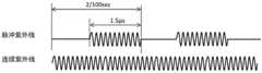
图2是比较脉冲紫外线和连续紫外线的持续时间而示出的图,在横轴取时间来示出。FIG. 2 is a graph showing a comparison of durations of pulsed ultraviolet rays and continuous ultraviolet rays, and is shown by taking time on the horizontal axis.
图3是表示在样品台载置晶片并施加静电吸附电压时的介电分离状况的简要图。3 is a schematic diagram showing the state of dielectric separation when a wafer is placed on a sample stage and an electrostatic attraction voltage is applied.
图4是晶片的顶视图,表示来自脉冲紫外线光源的紫外线照射位置和晶片上带电分布状况。FIG. 4 is a top view of the wafer, showing the irradiation position of ultraviolet rays from the pulsed ultraviolet light source and the state of charge distribution on the wafer.
图5是表示等离子处理装置的启动定时的序列的图,在纵轴取各部的导通/截止来表示,在横轴取时间来表示。5 is a diagram showing a sequence of activation timings of the plasma processing apparatus, in which the ON/OFF of each part is shown on the vertical axis, and the time is shown on the horizontal axis.
图6是表示点火判定以及点火时间记录的流程的流程图。FIG. 6 is a flowchart showing the flow of ignition determination and ignition timing recording.
附图标记说明Description of reference numerals
101 高频电源101 High frequency power supply
102 脉冲紫外线光源102 Pulsed UV Light Source
103 石英光纤103 Silica Fiber
104 波导管104 Waveguide
105 磁控管105 Magnetron
106 准直透镜106 Collimating lens
107 顶板107 Top plate
108 螺线管线圈108 Solenoid Coil
109 等离子109 Plasma
111 控制部111 Control Department
112 静电吸附电源112 Electrostatic adsorption power supply
113 样品台113 Sample stage
114 处理室114 Processing Room
115 脉冲紫外线光源115 Pulsed UV Light Source
116 LAN线缆116 LAN cable
117 微波以及紫外线提供口117 Microwave and UV-provided ports
118 工艺气体提供源118 Process gas supply source
300 晶片300 chips
301 内侧电极基材301 Inner electrode substrate
302 外侧电极基材302 Outer electrode substrate
303 喷涂膜303 Spray film
304 库伦引力304 Coulomb Gravity
306 脉冲紫外线306 Pulsed UV
401 脉冲紫外线的照射位置401 Irradiation position of pulsed UV light
403 晶片表面上的外侧区域403 Outer area on wafer surface
404 晶片表面上的中心区域404 Center area on wafer surface
具体实施方式Detailed ways
参考附图来说明本发明所涉及的实施方式的等离子处理装置。图1是在等离子生成单元中利用微波和磁场的微波ECR(Electron CyclotronResonance,电子回旋共振)等离子处理装置的简要截面图。特别,在等离子处理装置中,在使用低气体压力、低微波功率、低占空比等工艺条件的情况下,在工艺开始时不能合适地进行等离子点火,这成为重要的技术课题。根据本实施方式,在相关的工艺条件下也能提升等离子点火性。A plasma processing apparatus according to an embodiment of the present invention will be described with reference to the drawings. FIG. 1 is a schematic cross-sectional view of a microwave ECR (Electron Cyclotron Resonance, electron cyclotron resonance) plasma processing apparatus utilizing microwaves and a magnetic field in a plasma generating unit. In particular, in a plasma processing apparatus, when process conditions such as low gas pressure, low microwave power, and low duty ratio are used, plasma ignition cannot be properly performed at the start of the process, which is an important technical problem. According to the present embodiment, the plasma ignitability can also be improved under the relevant process conditions.
微波ECR等离子处理装置100具备:能将内部真空排气的处理室114;配置被处理物(也称作样品)即晶片300的样品台113;设于样品台113上方的石英等的微波以及紫外线提供口117;设于其上的波导管104;通过内置的第1高频电源提供高频电力而产生微波的磁控管105;设于波导管的窥视窗之上的脉冲紫外线光源102;设于处理室114的周围的螺线管线圈108;与样品台连接的静电吸附电源112;高频电源(第2高频电源)101;工艺气体提供源118;和控制部(处理器)111。The microwave ECR plasma processing apparatus 100 includes: a processing chamber 114 capable of evacuating the inside; a sample stage 113 on which a
作为脉冲紫外线光源,例如能使用输出5W且能出射波长185nm~2000nm的光的灯。能使用出射光当中紫外段(185nm~450nm)的光来进行后述的处理。As the pulsed ultraviolet light source, for example, a lamp capable of outputting light having a wavelength of 185 nm to 2000 nm with an output of 5 W can be used. The processing described later can be performed using light in the ultraviolet range (185 nm to 450 nm) in the outgoing light.
以下,说明利用微波ECR等离子处理装置100的等离子处理的工艺。首先,晶片300在被搬入处理室114内后,通过静电吸附电源112而被静电吸附在样品台113。接下来,由工艺气体提供源118将工艺气体经由气体导入口(图略)从簇射板119提供到处理室114内,通过真空泵(图略)调整成给定的压力。Hereinafter, the process of plasma processing by the microwave ECR plasma processing apparatus 100 will be described. First, after the
接下来,从磁控管105振荡频率2.45GHz的微波,使其通过波导管104传播到处理室114内。通过微波和由螺线管线圈108产生的磁场的作用来激发处理气体,由此在晶片300上部的空间生成等离子109。使用该等离子109进行搭载于样品台113的晶片300的蚀刻工艺。Next, microwaves having a frequency of 2.45 GHz are oscillated from the magnetron 105 and propagated into the processing chamber 114 through the waveguide 104 . The process gas is excited by the action of microwaves and the magnetic field generated by the solenoid coil 108 , thereby generating the plasma 109 in the space above the
在上述的微波ECR等离子处理装置中具备控制各器件的启动定时的系统。具体地,高频电源101、脉冲紫外线光源102、磁控管105、螺线管线圈108、静电吸附电源112、光检测器110等器件经由LAN(Local AreaNetwork)线缆116与控制部111连接,通过在控制部111中编排序列来分别控制这些器件。特别地,控制部111能对脉冲紫外线光源102进行脉冲调制,这里能调整脉冲间隔。The above-mentioned microwave ECR plasma processing apparatus includes a system for controlling the activation timing of each device. Specifically, devices such as the high-frequency power supply 101 , the pulsed ultraviolet light source 102 , the magnetron 105 , the solenoid coil 108 , the electrostatic adsorption power supply 112 , and the photodetector 110 are connected to the control unit 111 via a LAN (Local Area Network) cable 116 . These devices are individually controlled by arranging sequences in the control section 111 . In particular, the control unit 111 can perform pulse modulation on the pulsed ultraviolet light source 102, and the pulse interval can be adjusted here.
若使绕着由螺线管线圈108产生的磁场进行圆运动的频率和从外部投入的电磁波的频率一致,位于气体分子的外侧的电子就会因共振(ECR)而开始高速旋转运动。在该电子的动能为电离能量以上时,位于原子或分子的最外层的电子就会飞出,与相邻的原子或分子碰撞。电子的数量对碰撞的电子加上从分子或原子飞出的电子就会成为2倍。其结果,电子的数量如雪崩现象那样增加,若超过某阈值,就会形成等离子。但是,在工艺条件为低气体压力、低微波功率时,在原子或分子之间的距离远的情况下,或电离的电子不具有足以向旁边的原子或分子飞出的能量的情况下,等离子点火很困难。When the frequency of the circular motion around the magnetic field generated by the solenoid coil 108 is matched with the frequency of the electromagnetic wave injected from the outside, the electrons located outside the gas molecules start to rotate at high speed due to resonance (ECR). When the kinetic energy of the electron is equal to or higher than the ionization energy, the electron located in the outermost layer of the atom or molecule will fly out and collide with the adjacent atom or molecule. The number of electrons is double the number of colliding electrons plus the electrons flying off the molecule or atom. As a result, the number of electrons increases like an avalanche phenomenon, and when it exceeds a certain threshold, plasma is formed. However, when the process conditions are low gas pressure, low microwave power, when the distance between atoms or molecules is large, or when the ionized electrons do not have enough energy to fly to nearby atoms or molecules, the plasma Ignition is difficult.
在本实施方式中,在微波ECR等离子处理装置100设置脉冲紫外线光源102。如图2所示那样,从脉冲紫外线光源102以2/100秒间隔产生脉冲紫外线(照射脉冲状的紫外线)。紫外线的一个脉冲(称作闪烁)作为一例持续1.5μs,这时放出100mJ的能量。另外,脉冲紫外线的波形中的紫外线的脉冲的周期与紫外线的照射时间的比例尺不同,紫外线的照射时间相对于紫外线的脉冲的周期表示为约6667倍。在本规格下,若使脉冲紫外线的间隔至少为1/155秒以上,就不会使晶片温度实质上升。因此,将脉冲紫外线的间隔至少设为1/150秒以上即可。In this embodiment, a pulsed ultraviolet light source 102 is provided in the microwave ECR plasma processing apparatus 100 . As shown in FIG. 2 , pulsed ultraviolet rays (pulsed ultraviolet rays are irradiated) are generated from the pulsed ultraviolet light source 102 at intervals of 2/100 seconds. A pulse of ultraviolet light (called a flicker) lasts for example for 1.5 μs, at which time 100 mJ of energy is released. In the waveform of the pulsed ultraviolet rays, the period of the ultraviolet pulse is different from the scale of the irradiation time of the ultraviolet rays, and the irradiation time of the ultraviolet rays is expressed as about 6667 times the period of the pulse of the ultraviolet rays. Under this standard, if the interval of pulsed ultraviolet rays is at least 1/155 second or more, the wafer temperature will not substantially increase. Therefore, the interval of the pulsed ultraviolet rays may be at least 1/150 second or more.
若脉冲紫外线光源102产生脉冲紫外线,则产生的脉冲紫外线经由石英光纤(例如直径:0.8mm)103和准直透镜(例如直径:3mm、扩散性tan(a):0.08,其中,a=纤径/焦点)106与微波入射方向平行且朝向被处理前的晶片表面入射到处理室114。由此,位于工艺气体分子或原子的外层的电子通过从脉冲紫外线吸收光子而被激发。If the pulsed ultraviolet light source 102 generates pulsed ultraviolet rays, the generated pulsed ultraviolet rays pass through a silica fiber (eg diameter: 0.8 mm) 103 and a collimating lens (eg diameter: 3 mm, diffusivity tan(a): 0.08, where a=fiber diameter) /focal point) 106 is incident into the processing chamber 114 parallel to the microwave incident direction and toward the surface of the wafer before being processed. Thereby, electrons located in the outer layers of process gas molecules or atoms are excited by absorbing photons from the pulsed UV light.
进而,若通过了工艺气体的脉冲紫外线入射到晶片表面,就会在晶片表面引起光电效应,由此产生自由电子。因而,能通过注入微波,使用点火前在处理室114被激发的电子、或自由电子,来改善等离子的点火性。Furthermore, when the pulsed ultraviolet rays passed through the process gas are incident on the wafer surface, a photoelectric effect is induced on the wafer surface, thereby generating free electrons. Therefore, by injecting microwaves, the ignitability of the plasma can be improved by using electrons or free electrons excited in the processing chamber 114 before ignition.
上述那样在导入微波和磁场前对工艺气体照射紫外线是为了提高位于工艺气体分子或原子的外侧的电子的能级(激发)。一般,电子的激发状态不稳定,仅能在激发状态停留10-8s。并且,若有点火的火种,等离子就会通过雪崩现象而瞬间生成。因而,比起连续的紫外线照射,瞬间的光输出高的脉冲紫外线照射更能瞬间激发大量的气体,适于实现等离子点火的改善。The reason for irradiating the process gas with ultraviolet rays before introducing the microwave and the magnetic field as described above is to increase the energy level (excitation) of electrons located outside the molecules or atoms of the process gas. Generally, the excited state of electrons is unstable and can only stay in the excited state for 10-8 s. And, if there is a kind of ignition, the plasma will be instantly generated by the avalanche phenomenon. Therefore, compared to continuous ultraviolet irradiation, pulsed ultraviolet irradiation with a high instantaneous light output can instantly excite a large amount of gas, which is suitable for improving plasma ignition.
进而,能使用在电容器中积存电荷来进行发光的类型的脉冲紫外线光源,由此不再为了产生脉冲紫外线而需要光源的预热,易于配合处理的动作定时,适于应用。另外,在以相同的100mJ的功率连续地发出紫外线的情况下,需要约70KW的大型电源,等离子装置的设备成本变高,也不能实现节能。根据这样的观点,也期望使用脉冲紫外线。Furthermore, a pulsed ultraviolet light source that emits light by accumulating electric charges in a capacitor can be used, which eliminates the need for preheating of the light source to generate pulsed ultraviolet rays, and is suitable for applications because it is easy to match the operation timing of processing. In addition, when the ultraviolet rays are continuously emitted at the same power of 100 mJ, a large power supply of about 70 kW is required, the equipment cost of the plasma apparatus increases, and energy saving cannot be achieved. From such a viewpoint, it is also desirable to use pulsed ultraviolet rays.
在图3示出设于样品台上的电极的放大图。该电极具有圆盘状的内侧电极基材301、包围其的环状的外侧电极基材302和喷涂膜303。若静电吸附电源112(图1)对电分离的两个电极基材301、302分别施加极性不同的电压(例如+1500V和-1500V),就会因感应电而在喷涂膜303的表面和晶片300的背面分别在与电极基材301、302对应的区域产生正负的电位。晶片300由通过该电位产生的库伦引力304吸附在电极表面。另外,关于设于样品台上的电极,可以仅设置具有负的电位的一极的电极构件。An enlarged view of the electrodes provided on the sample stage is shown in FIG. 3 . This electrode has a disk-shaped
晶片300在被载置于样品台113(图1)之上后,通过静电吸附电源112被静电吸附在样品台113。更具体地,如图3所示那样,在对喷涂膜303施加负电压的情况下,晶片300的中央表面因感应电而具有负的电位。即,成为电子丰富存在于晶片300的中央表面的状态。在此,若对丰富具有电子的晶片300的中央表面照射脉冲紫外线306,就会因光电效应而使电子从晶片300的中央表面飞出,飞出的电子通过晶片300的表面上的负电位被向工艺气体加速。进而,电子在ECR面附近通过微波和磁场被加速,成为等离子点火的火种。After the
另外,若对内侧电极基材301施加负的电压,则与内侧电极基材301对应的被静电吸附的晶片300的表面的中心区域404(图4)具有负电荷,并且与外侧电极基材302对应的晶片300的表面的外侧区域403(图4)具有正的电荷。因而,优选将脉冲紫外线的照射位置401设置在被静电吸附的晶片300的具有负电荷的中心区域404的上方,将脉冲紫外线照射到上述的具有负电荷的区域(负的带电区域)。另外,优选使脉冲紫外线电源在静电吸附要处理的晶片300之前动作。In addition, when a negative voltage is applied to the
在此,在微波ECR等离子处理装置中,在将从准直透镜到晶片的距离设为约785mm时,若如上述那样经由光纤103和准直透镜106将脉冲紫外线照射到晶片表面,晶片表面的被照射范围就成为直径6cm的圆形区域。在无视传播中的光损失的情况下,在照射时间1.5μs期间在晶片表面受到的光的强度成为161mJ/s/cm2。灯加热所赋予的热量是光强度的1/10程度(16.1mJ/s/cm2),由于与来自处理中等离子的热量(500mJ/s/cm2)相比要小,因此晶片表面的温度几乎不改变。与此相对,若以100mJ的功率连续照射1sec,则抵达晶片表面的光的强度成为41551mJ/s/cm2,晶片表面温度有可能会上升。因而,为了不使晶片表面温度上升地对点火给予足够的能量,期望使用脉冲紫外线。Here, in the microwave ECR plasma processing apparatus, when the distance from the collimator lens to the wafer is set to be about 785 mm, if pulsed ultraviolet rays are irradiated to the wafer surface via the optical fiber 103 and the collimator lens 106 as described above, the The irradiated area becomes a circular area with a diameter of 6 cm. The intensity of light received on the wafer surface during the irradiation time of 1.5 μs was 161 mJ/s/cm2 , ignoring light loss during propagation. The heat given by the lamp heating is about 1/10 of the light intensity (16.1 mJ/s/cm2 ), and since it is smaller than the heat from the plasma in the process (500 mJ/s/cm2 ), the temperature of the wafer surface is hardly changed. On the other hand, if the power of 100 mJ is continuously irradiated for 1 sec, the intensity of the light reaching the wafer surface becomes 41551 mJ/s/cm2 , and the wafer surface temperature may increase. Therefore, in order to give sufficient energy to ignition without raising the wafer surface temperature, it is desirable to use pulsed ultraviolet rays.
为了不使脉冲紫外线和微波在传播中途损失增大,期望在紫外线传播中使用光纤103,进而,优选对位于处理室上的顶板107和簇射板119使用石英制品。In order not to increase the loss of pulsed ultraviolet rays and microwaves during propagation, it is desirable to use the optical fiber 103 for ultraviolet propagation, and it is preferable to use quartz products for the ceiling plate 107 and the shower plate 119 on the processing chamber.
在使用被脉冲调制的紫外线来照射工艺气体以及晶片表面的负带电区域时,为了验证等离子的点火改善效果,而使用上述的微波ECR等离子处理装置100以多种方案来实施点火改善确认实验。由于是验证等离子点火改善效果的实验,因此准备三个种类的处理模式(参考图5),准备两个种类的处理条件(参考表1、2)。In order to verify the effect of improving plasma ignition when irradiating a process gas and a negatively charged region on the wafer surface with pulsed ultraviolet rays, various experiments were performed to confirm ignition improvement using the microwave ECR plasma processing apparatus 100 described above. Since it was an experiment to verify the effect of improving plasma ignition, three types of processing modes (refer to FIG. 5 ) and two types of processing conditions (refer to Tables 1 and 2) were prepared.
说明利用上述的微波ECR等离子处理装置100的确认实验中所使用的三个处理模式(也仅称作模式)。在图5中,ESC是指静电吸附电源的驱动电压。在图5(a)所示的处理模式1中,将被处理前的晶片运送到处理室114,在放置在样品台113的电极之上的状态下,首先,在施加ESC电压而使晶片被吸附后,导入工艺气体,通过真空泵(图略)调整成给定的压力,通过磁控管驱动而导入给定微波和磁场,使等离子点火。在处理模式1中不进行脉冲紫外线的照射。Three processing modes (also simply referred to as modes) used in the confirmation experiment using the microwave ECR plasma processing apparatus 100 described above will be described. In FIG. 5, ESC refers to the driving voltage of the electrostatic adsorption power supply. In the processing mode 1 shown in FIG. 5( a ), the wafer before being processed is transported to the processing chamber 114 and placed on the electrodes of the sample stage 113 . First, an ESC voltage is applied to cause the wafer to be After adsorption, the process gas is introduced, adjusted to a given pressure by a vacuum pump (not shown in the figure), and a given microwave and magnetic field are introduced by the magnetron drive to ignite the plasma. In the treatment mode 1, the irradiation of pulsed ultraviolet rays is not performed.
另一方面,在图5(b)所示的处理模式2中,将被处理前的晶片运送到处理室114,在放置在样品台113的电极之上的状态下,首先,在施加ESC电压而使晶片被吸附后,导入工艺气体,通过真空泵(图略)调整成给定的压力,进而,使脉冲紫外线光源(102或115)动作,接下来,通过磁控管驱动而导入给定的微波和磁场,使等离子点火。On the other hand, in the
进而,在图5(c)所示的处理模式3中,将被处理前的晶片运送到处理室114,放置在样品台113的电极之上,首先,使脉冲紫外线光源(102或115)动作,接着,施加ESC电压而使晶片被吸附,控制部111之后导入工艺气体,通过真空泵(图略)调整成给定的压力,通过磁控管驱动而导入给定微波和磁场,使等离子点火。Furthermore, in the processing mode 3 shown in FIG. 5( c ), the wafer before being processed is transported to the processing chamber 114 , placed on the electrodes of the sample stage 113 , and first, the pulsed ultraviolet light source ( 102 or 115 ) is operated Next, an ESC voltage is applied to attract the wafer, and the control unit 111 then introduces a process gas, adjusts the pressure to a predetermined pressure by a vacuum pump (not shown), and is driven by a magnetron to introduce a predetermined microwave and a magnetic field to ignite the plasma.
说明利用上述的微波ECR等离子处理装置100的确认实验用的两个处理条件。Two processing conditions for the confirmation experiment using the microwave ECR plasma processing apparatus 100 described above will be described.
表在1和表2示出两个种类的处理条件。处理条件的参数被称作方案,进行基于表1、2所示的方案的动作。在方案1中,将Cl2用作工艺气体,流量设为150ml/min,气体压力和微波功率分别设定为0.5Pa和1000W。Tables 1 and 2 show two kinds of treatment conditions. The parameters of the processing conditions are referred to as plans, and operations based on the plans shown in Tables 1 and 2 are performed. In scheme1 , Cl2 was used as the process gas, the flow rate was set to 150ml/min, and the gas pressure and microwave power were set to 0.5Pa and 1000W, respectively.
【表1】【Table 1】
处理条件Processing conditions

实验结果Experimental results

在方案2中,将Cl2和CH3F用作工艺气体,流量分别将Cl2设为40ml/min、将CH3F设为150ml/min,气体压力和微波功率分别设定为0.2Pa和600W。方案2与方案1相比,气体压力和微波功率低,比较难以点火。In
【表2】【Table 2】
处理条件Processing conditions

实验结果Experimental results

在图6示出由控制部111进行的点火时间的判定和记录的处理流程。由图1的光检测器110监视处理室内的发光状况(发光等级),将其数据送到控制部111。在步骤S01中开始脉冲紫外线以及给定微波和磁场的导入,并且控制部111使计数器(未图示)开始,首先,若在步骤S02中判断为是经过10s的计数时间之前(步骤S02“是”),则在步骤S03中,由控制部111对发光数据进行分析。若发光等级超过某阈值(步骤S03“是”),则控制部111判定为等离子点火,在步骤S04中开始处理工艺,并停止计数器,将其计数时间作为等离子点火时间存储。FIG. 6 shows the processing flow of the determination and recording of the ignition timing by the control unit 111 . The light emission state (light emission level) in the processing chamber is monitored by the photodetector 110 of FIG. 1 , and the data thereof is sent to the control unit 111 . In step S01, the introduction of pulsed ultraviolet rays, predetermined microwaves, and magnetic fields is started, and the control unit 111 starts a counter (not shown). First, if it is determined in step S02 that it is before the count time of 10 s elapses (step S02 "Yes" ”), then in step S03, the control unit 111 analyzes the light emission data. When the light emission level exceeds a certain threshold (YES in step S03 ), the control unit 111 determines that the plasma ignition is performed, starts the process in step S04 , stops the counter, and stores the counted time as the plasma ignition time.
另一方面,若发光等级未超过某阈值(步骤S03“否”),就使流程回到步骤S02,一边继续导入脉冲紫外线以及给定微波和磁场,一边继续进行计数,在步骤S03中由控制部111继续监视发光等级。On the other hand, if the light emission level does not exceed a certain threshold (“NO” in step S03), the flow returns to step S02, and continues to count while continuously introducing pulsed ultraviolet rays, predetermined microwaves and magnetic fields, and in step S03 controlled by Section 111 continues to monitor the light emission level.
若在发光等级的监视中,控制部111判断为从脉冲紫外线以及给定微波和磁场的导入开始经过了10s的计数时间(步骤S02“否”),则判断为等离子点火失败,在步骤S05中视作错误。在这样的情况下,控制部111将等离子点火时间作为10.1秒来存储。If the control unit 111 determines that a count time of 10 s has elapsed since the introduction of the pulsed ultraviolet rays, the predetermined microwave and the magnetic field during the monitoring of the emission level (NO in step S02), then it is determined that the plasma ignition has failed, and in step S05 considered an error. In such a case, the control unit 111 stores the plasma ignition time as 10.1 seconds.
[关于点火改善性以及照射方向依赖性的研讨][Study on ignition improvement and irradiation direction dependence]
进行如下的比较试验,确认点火改善效果。The following comparative tests were performed to confirm the ignition improvement effect.
·图5(a)的处理模式1(无紫外线)· Treatment mode 1 (without UV light) in Fig. 5(a)
·图5(b)的处理模式2(其中,使用位于装置侧方的脉冲紫外线光源115,从侧方使脉冲紫外线入射到处理室114)
·图5(b)的处理模式2(其中,使用位于装置上方的脉冲紫外线光源102,从上方使脉冲紫外线入射到处理室114)
如表1所示那样,以处理模式1对Si(硅)晶片实施10次方案1的处理的结果是,10次所相应的点火时间的平均值是1.13s。接下来,以处理模式2对Si晶片实施10次方案1的处理的结果是,10次所相应的点火时间的平均值是1.00s。最后,以处理模式2对Si晶片实施10次方案1的处理的结果是,10次所相应的点火时间的平均值是0.64s。As shown in Table 1, when the Si (silicon) wafer was subjected to 10 times of the treatment of the scheme 1 in the treatment mode 1, the average value of the ignition time corresponding to the 10 times was 1.13 s. Next, when the Si wafer was subjected to 10 times of the treatment of the scheme 1 in the
根据以上的结果可知,与不照射脉冲紫外线的情况相比,照射脉冲紫外线的情况提升了等离子点火性。另外,可知,与从侧方照射脉冲紫外线相比,从上方(朝向Si晶片和工艺气体)照射能进一步改善点火性。From the above results, it was found that the plasma ignitability was improved when the pulsed ultraviolet rays were irradiated compared to the case where the pulsed ultraviolet rays were not irradiated. In addition, it was found that irradiation from above (toward the Si wafer and process gas) can further improve ignitability compared to irradiation of pulsed ultraviolet rays from the side.
[关于点火改善性的研讨][Study on Ignition Improvement Properties]
进行如下的比较实验,确认点火改善效果。The following comparative experiments were performed to confirm the ignition improvement effect.
·图5(a)的处理模式1(无紫外线)· Treatment mode 1 (without UV light) in Fig. 5(a)
·图5(c)的处理模式3(其中,使用位于装置上方的脉冲紫外线光源102,从上方使脉冲紫外线入射到处理室114)Treatment mode 3 of FIG. 5( c ) (in which the pulsed ultraviolet light source 102 located above the apparatus is used, and the pulsed ultraviolet light is incident on the treatment chamber 114 from above)
如表2所示那样,以处理模式1对Si晶片实施10次方案2的处理的结果是,10次所相应的点火时间的平均值是4.67s。另一方面,以处理模式3对Si晶片实施10次方案2的处理的结果是,10次所相应的点火时间的平均值是0.87s。As shown in Table 2, when the Si wafer was subjected to 10 times of the treatment of the
根据以上的结果,即使改变方案,也是与不照射脉冲紫外线的情况相比,照射脉冲紫外线的情况更加提升等离子点火性。From the above results, even if the scheme is changed, the plasma ignitability is more improved in the case of irradiating pulsed ultraviolet rays than in the case of not irradiating pulsed ultraviolet rays.
通过以上的确认实验可知,使用脉冲紫外线不管照射工艺气体和晶片表面的哪一者,都能看到点火改善效果。另外,由于重叠两个效果能引出最佳的点火效果,因此优选使脉冲紫外线光源在晶片的静电吸附前动作。这是因为,通过在晶片的静电吸附前照射紫外线,飞出到晶片上的电子会增加。From the above confirmation experiments, it was found that the ignition improvement effect was observed regardless of whether the process gas or the wafer surface was irradiated with pulsed ultraviolet rays. In addition, since the best ignition effect can be obtained by superimposing the two effects, it is preferable to operate the pulsed ultraviolet light source before the electrostatic adsorption of the wafer. This is because, by irradiating ultraviolet rays before electrostatic adsorption of the wafer, electrons that fly out to the wafer increase.
具体期望以下的工序。在本实施方式的微波ECR等离子处理装置100中,首先,使脉冲紫外线光源102动作,开始照射脉冲紫外线。接下来,通过由静电吸附电源112对样品台113施加直流电压而使处理前的晶片300被静电吸附。之后,提供工艺气体,通过真空泵调整成给定的压力。然后,将从磁控管105产生的微波和从螺线管线圈108产生的磁场导入到处理室内,进行等离子点火。若引发等离子点火,则之后就会连续生成等离子。通过前述的等离子对半导体晶片实施给定的工艺。Specifically, the following steps are desired. In the microwave ECR plasma processing apparatus 100 of the present embodiment, first, the pulsed ultraviolet light source 102 is operated, and the irradiation of pulsed ultraviolet rays is started. Next, the
另外,在上述的实施方式中,将电子回旋共振(ECR)设为等离子生成单元进行了说明,但并不限定于此,还能运用于激发工艺气体的其他等离子放电方法中。例如,能在电容耦合等离子(CCP)、感应耦合等离子(ICP)、电磁感应耦合等离子(EMCP)等等离子生成方式中运用本发明。In addition, in the above-mentioned embodiment, the electron cyclotron resonance (ECR) was described as the plasma generation unit, but the invention is not limited to this, and it can be applied to other plasma discharge methods for exciting the process gas. For example, the present invention can be applied to plasma generation methods such as capacitively coupled plasma (CCP), inductively coupled plasma (ICP), electromagnetically inductively coupled plasma (EMCP), and the like.
另外,本发明并不限定于上述的实施方式,而包含各种变形例。例如上述的实施方式为了易于理解地说明本发明而详细进行了说明,但不一定限定于具备说明的全部结构。另外,能将某实施方式中的结构的一部分置换成其他实施方式的结构,另外,还能在某实施方式的结构中加进其他实施方式的结构。另外,还能对各实施方式中的结构的一部分进行其他结构的追加、删除、置换。In addition, this invention is not limited to the above-mentioned embodiment, Various modification examples are included. For example, the above-described embodiments have been described in detail in order to explain the present invention in an easy-to-understand manner, but the present invention is not necessarily limited to having all the configurations described. Moreover, a part of the structure in a certain embodiment can be replaced with the structure of another embodiment, and the structure of another embodiment can also be added to the structure of a certain embodiment. In addition, addition, deletion, and replacement of other structures can be performed on a part of the structures in each embodiment.
Claims (6)
Applications Claiming Priority (2)
| Application Number | Priority Date | Filing Date | Title |
|---|---|---|---|
| JP2018-138374 | 2018-07-24 | ||
| JP2018138374AJP6913060B2 (en) | 2018-07-24 | 2018-07-24 | Plasma processing equipment and plasma processing method |
Publications (2)
| Publication Number | Publication Date |
|---|---|
| CN110752136Atrue CN110752136A (en) | 2020-02-04 |
| CN110752136B CN110752136B (en) | 2023-06-23 |
Family
ID=69178229
Family Applications (1)
| Application Number | Title | Priority Date | Filing Date |
|---|---|---|---|
| CN201910037872.8AActiveCN110752136B (en) | 2018-07-24 | 2019-01-15 | Plasma processing device and plasma processing method |
Country Status (5)
| Country | Link |
|---|---|
| US (1) | US10872774B2 (en) |
| JP (1) | JP6913060B2 (en) |
| KR (1) | KR102190143B1 (en) |
| CN (1) | CN110752136B (en) |
| TW (1) | TWI736829B (en) |
Families Citing this family (3)
| Publication number | Priority date | Publication date | Assignee | Title |
|---|---|---|---|---|
| WO2020012704A1 (en)* | 2019-03-06 | 2020-01-16 | 株式会社日立ハイテクノロジーズ | Plasma processing device, plasma processing method, and ecr height monitor |
| US11348784B2 (en) | 2019-08-12 | 2022-05-31 | Beijing E-Town Semiconductor Technology Co., Ltd | Enhanced ignition in inductively coupled plasmas for workpiece processing |
| JP2022110892A (en) | 2021-01-19 | 2022-07-29 | 東京エレクトロン株式会社 | Plasma processing apparatus and plasma processing method |
Citations (9)
| Publication number | Priority date | Publication date | Assignee | Title |
|---|---|---|---|---|
| JPH04137530A (en)* | 1990-09-27 | 1992-05-12 | Matsushita Electric Ind Co Ltd | Dry etching method |
| US5963840A (en)* | 1996-11-13 | 1999-10-05 | Applied Materials, Inc. | Methods for depositing premetal dielectric layer at sub-atmospheric and high temperature conditions |
| KR20020064028A (en)* | 2001-01-31 | 2002-08-07 | 한빛 세마텍(주) | Cleaning and surface treatment equipment by pulsed ultra-violet light radiation |
| US20050087296A1 (en)* | 2003-03-26 | 2005-04-28 | Tokyo Electron Limited | Processor |
| CN1669126A (en)* | 2002-07-10 | 2005-09-14 | 月岛机械株式会社 | Surface treating method for substrate |
| US20060086699A1 (en)* | 1997-06-26 | 2006-04-27 | Mks Instruments, Inc. | Method and apparatus for processing metal bearing gases |
| CN1913741A (en)* | 2005-08-10 | 2007-02-14 | 东京毅力科创株式会社 | Control method of plasma treatment device and plasma treatment device |
| US20140262755A1 (en)* | 2013-03-13 | 2014-09-18 | Applied Materials, Inc. | Uv-assisted reactive ion etch for copper |
| CN107644830A (en)* | 2016-07-20 | 2018-01-30 | 株式会社迪思科 | The absorption confirmation method of chip, depart from confirmation method and decompression processing device |
Family Cites Families (14)
| Publication number | Priority date | Publication date | Assignee | Title |
|---|---|---|---|---|
| US5138520A (en)* | 1988-12-27 | 1992-08-11 | Symetrix Corporation | Methods and apparatus for material deposition |
| JPH0547713A (en)* | 1991-08-20 | 1993-02-26 | Tadahiro Omi | Apparatus for plasma processing |
| JPH06349776A (en) | 1993-06-14 | 1994-12-22 | Hitachi Ltd | Semiconductor manufacturing apparatus |
| JPH08139004A (en)* | 1994-11-14 | 1996-05-31 | Sony Corp | Plasma treatment apparatus and plasma treatment method |
| US5994209A (en)* | 1996-11-13 | 1999-11-30 | Applied Materials, Inc. | Methods and apparatus for forming ultra-shallow doped regions using doped silicon oxide films |
| US6039834A (en)* | 1997-03-05 | 2000-03-21 | Applied Materials, Inc. | Apparatus and methods for upgraded substrate processing system with microwave plasma source |
| US7300859B2 (en)* | 1999-02-01 | 2007-11-27 | Sigma Laboratories Of Arizona, Llc | Atmospheric glow discharge with concurrent coating deposition |
| US7100532B2 (en)* | 2001-10-09 | 2006-09-05 | Plasma Control Systems, Llc | Plasma production device and method and RF driver circuit with adjustable duty cycle |
| JP2008519416A (en)* | 2004-11-08 | 2008-06-05 | エム ケー エス インストルメンツ インコーポレーテッド | Method and apparatus for treating metal-containing gases |
| US20140094038A1 (en)* | 2007-03-30 | 2014-04-03 | Novellus Systems, Inc. | Enhancing adhesion of cap layer films |
| KR100915613B1 (en)* | 2007-06-26 | 2009-09-07 | 삼성전자주식회사 | Pulse Plasma Matching System and Method |
| US8633459B2 (en)* | 2011-03-02 | 2014-01-21 | Cymer, Llc | Systems and methods for optics cleaning in an EUV light source |
| US20140116335A1 (en)* | 2012-10-31 | 2014-05-01 | Asm Ip Holding B.V. | UV Irradiation Apparatus with Cleaning Mechanism and Method for Cleaning UV Irradiation Apparatus |
| US9576810B2 (en)* | 2013-10-03 | 2017-02-21 | Applied Materials, Inc. | Process for etching metal using a combination of plasma and solid state sources |
- 2018
- 2018-07-24JPJP2018138374Apatent/JP6913060B2/enactiveActive
- 2018-12-13KRKR1020180160647Apatent/KR102190143B1/enactiveActive
- 2019
- 2019-01-15CNCN201910037872.8Apatent/CN110752136B/enactiveActive
- 2019-01-25TWTW108102827Apatent/TWI736829B/enactive
- 2019-02-26USUS16/286,303patent/US10872774B2/enactiveActive
Patent Citations (9)
| Publication number | Priority date | Publication date | Assignee | Title |
|---|---|---|---|---|
| JPH04137530A (en)* | 1990-09-27 | 1992-05-12 | Matsushita Electric Ind Co Ltd | Dry etching method |
| US5963840A (en)* | 1996-11-13 | 1999-10-05 | Applied Materials, Inc. | Methods for depositing premetal dielectric layer at sub-atmospheric and high temperature conditions |
| US20060086699A1 (en)* | 1997-06-26 | 2006-04-27 | Mks Instruments, Inc. | Method and apparatus for processing metal bearing gases |
| KR20020064028A (en)* | 2001-01-31 | 2002-08-07 | 한빛 세마텍(주) | Cleaning and surface treatment equipment by pulsed ultra-violet light radiation |
| CN1669126A (en)* | 2002-07-10 | 2005-09-14 | 月岛机械株式会社 | Surface treating method for substrate |
| US20050087296A1 (en)* | 2003-03-26 | 2005-04-28 | Tokyo Electron Limited | Processor |
| CN1913741A (en)* | 2005-08-10 | 2007-02-14 | 东京毅力科创株式会社 | Control method of plasma treatment device and plasma treatment device |
| US20140262755A1 (en)* | 2013-03-13 | 2014-09-18 | Applied Materials, Inc. | Uv-assisted reactive ion etch for copper |
| CN107644830A (en)* | 2016-07-20 | 2018-01-30 | 株式会社迪思科 | The absorption confirmation method of chip, depart from confirmation method and decompression processing device |
Also Published As
| Publication number | Publication date |
|---|---|
| TWI736829B (en) | 2021-08-21 |
| KR102190143B1 (en) | 2020-12-11 |
| JP6913060B2 (en) | 2021-08-04 |
| US20200035445A1 (en) | 2020-01-30 |
| CN110752136B (en) | 2023-06-23 |
| US10872774B2 (en) | 2020-12-22 |
| TW202008855A (en) | 2020-02-16 |
| JP2020017586A (en) | 2020-01-30 |
| KR20200011342A (en) | 2020-02-03 |
Similar Documents
| Publication | Publication Date | Title |
|---|---|---|
| US6861643B2 (en) | Neutral particle beam processing apparatus | |
| CN110419091A (en) | Deposition or treatment of diamond-like carbon in plasma reactors and plasma reactors | |
| US9111728B2 (en) | E-beam enhanced decoupled source for semiconductor processing | |
| US10395903B2 (en) | Self-sustained non-ambipolar direct current (DC) plasma at low power | |
| CN112703577A (en) | Enhanced ignition in inductively coupled plasma for workpiece processing | |
| US20120258601A1 (en) | E-Beam Enhanced Decoupled Source for Semiconductor Processing | |
| US20120258607A1 (en) | E-Beam Enhanced Decoupled Source for Semiconductor Processing | |
| JP2002289583A (en) | Beam treatment device | |
| CN110752136B (en) | Plasma processing device and plasma processing method | |
| SG193943A1 (en) | E-beam enhanced decoupled source for semiconductor processing | |
| JP5280440B2 (en) | Conformal doping using high neutral density plasma implantation | |
| TWI835756B (en) | Substrate processing method and substrate processing apparatus | |
| JP2010532919A5 (en) | ||
| JP2002289581A (en) | Neutral beam processing equipment | |
| US8053747B2 (en) | Substrate processing apparatus and cleaning method of the same | |
| JP4073173B2 (en) | Neutral particle beam processing equipment | |
| US20200006036A1 (en) | Methods and apparatus for electron beam etching process | |
| WO2012142038A1 (en) | E-beam enhanced decoupled source for semiconductor processing | |
| KR20220105129A (en) | Plasma processing apparatus and plasma processing method | |
| JP2000058292A (en) | Method and device for plasma treatment | |
| JPH0221296B2 (en) | ||
| JPS62216639A (en) | Device for treating surface |
Legal Events
| Date | Code | Title | Description |
|---|---|---|---|
| PB01 | Publication | ||
| PB01 | Publication | ||
| SE01 | Entry into force of request for substantive examination | ||
| SE01 | Entry into force of request for substantive examination | ||
| GR01 | Patent grant | ||
| GR01 | Patent grant |