CN110751900A - Display device and electronic apparatus - Google Patents
Display device and electronic apparatusDownload PDFInfo
- Publication number
- CN110751900A CN110751900ACN201911049442.4ACN201911049442ACN110751900ACN 110751900 ACN110751900 ACN 110751900ACN 201911049442 ACN201911049442 ACN 201911049442ACN 110751900 ACN110751900 ACN 110751900A
- Authority
- CN
- China
- Prior art keywords
- display
- electrochromic
- strips
- layer
- conductive layer
- Prior art date
- Legal status (The legal status is an assumption and is not a legal conclusion. Google has not performed a legal analysis and makes no representation as to the accuracy of the status listed.)
- Granted
Links
Images


Classifications
- G—PHYSICS
- G09—EDUCATION; CRYPTOGRAPHY; DISPLAY; ADVERTISING; SEALS
- G09F—DISPLAYING; ADVERTISING; SIGNS; LABELS OR NAME-PLATES; SEALS
- G09F9/00—Indicating arrangements for variable information in which the information is built-up on a support by selection or combination of individual elements
- G—PHYSICS
- G02—OPTICS
- G02F—OPTICAL DEVICES OR ARRANGEMENTS FOR THE CONTROL OF LIGHT BY MODIFICATION OF THE OPTICAL PROPERTIES OF THE MEDIA OF THE ELEMENTS INVOLVED THEREIN; NON-LINEAR OPTICS; FREQUENCY-CHANGING OF LIGHT; OPTICAL LOGIC ELEMENTS; OPTICAL ANALOGUE/DIGITAL CONVERTERS
- G02F1/00—Devices or arrangements for the control of the intensity, colour, phase, polarisation or direction of light arriving from an independent light source, e.g. switching, gating or modulating; Non-linear optics
- G02F1/01—Devices or arrangements for the control of the intensity, colour, phase, polarisation or direction of light arriving from an independent light source, e.g. switching, gating or modulating; Non-linear optics for the control of the intensity, phase, polarisation or colour
- G02F1/13—Devices or arrangements for the control of the intensity, colour, phase, polarisation or direction of light arriving from an independent light source, e.g. switching, gating or modulating; Non-linear optics for the control of the intensity, phase, polarisation or colour based on liquid crystals, e.g. single liquid crystal display cells
- G02F1/133—Constructional arrangements; Operation of liquid crystal cells; Circuit arrangements
- G02F1/1333—Constructional arrangements; Manufacturing methods
- G02F1/1335—Structural association of cells with optical devices, e.g. polarisers or reflectors
- G02F1/133528—Polarisers
- G—PHYSICS
- G02—OPTICS
- G02F—OPTICAL DEVICES OR ARRANGEMENTS FOR THE CONTROL OF LIGHT BY MODIFICATION OF THE OPTICAL PROPERTIES OF THE MEDIA OF THE ELEMENTS INVOLVED THEREIN; NON-LINEAR OPTICS; FREQUENCY-CHANGING OF LIGHT; OPTICAL LOGIC ELEMENTS; OPTICAL ANALOGUE/DIGITAL CONVERTERS
- G02F1/00—Devices or arrangements for the control of the intensity, colour, phase, polarisation or direction of light arriving from an independent light source, e.g. switching, gating or modulating; Non-linear optics
- G02F1/01—Devices or arrangements for the control of the intensity, colour, phase, polarisation or direction of light arriving from an independent light source, e.g. switching, gating or modulating; Non-linear optics for the control of the intensity, phase, polarisation or colour
- G02F1/15—Devices or arrangements for the control of the intensity, colour, phase, polarisation or direction of light arriving from an independent light source, e.g. switching, gating or modulating; Non-linear optics for the control of the intensity, phase, polarisation or colour based on an electrochromic effect
- G02F1/153—Constructional details
- G02F1/157—Structural association of cells with optical devices, e.g. reflectors or illuminating devices
- H—ELECTRICITY
- H10—SEMICONDUCTOR DEVICES; ELECTRIC SOLID-STATE DEVICES NOT OTHERWISE PROVIDED FOR
- H10K—ORGANIC ELECTRIC SOLID-STATE DEVICES
- H10K50/00—Organic light-emitting devices
- H10K50/10—OLEDs or polymer light-emitting diodes [PLED]
- H10K50/19—Tandem OLEDs
- H—ELECTRICITY
- H10—SEMICONDUCTOR DEVICES; ELECTRIC SOLID-STATE DEVICES NOT OTHERWISE PROVIDED FOR
- H10K—ORGANIC ELECTRIC SOLID-STATE DEVICES
- H10K50/00—Organic light-emitting devices
- H10K50/80—Constructional details
- H10K50/85—Arrangements for extracting light from the devices
- H—ELECTRICITY
- H10—SEMICONDUCTOR DEVICES; ELECTRIC SOLID-STATE DEVICES NOT OTHERWISE PROVIDED FOR
- H10K—ORGANIC ELECTRIC SOLID-STATE DEVICES
- H10K50/00—Organic light-emitting devices
- H10K50/80—Constructional details
- H10K50/868—Arrangements for polarized light emission
Landscapes
- Physics & Mathematics (AREA)
- Nonlinear Science (AREA)
- Optics & Photonics (AREA)
- General Physics & Mathematics (AREA)
- Mathematical Physics (AREA)
- Chemical & Material Sciences (AREA)
- Crystallography & Structural Chemistry (AREA)
- Engineering & Computer Science (AREA)
- Theoretical Computer Science (AREA)
- Electrochromic Elements, Electrophoresis, Or Variable Reflection Or Absorption Elements (AREA)
Abstract
Description
Translated fromChinese技术领域technical field
本申请涉及电子技术领域,特别涉及一种显示装置和电子设备。The present application relates to the field of electronic technology, and in particular, to a display device and electronic equipment.
背景技术Background technique
随着通信技术的发展,诸如智能手机等电子设备越来越普及。在电子设备的使用过程中,电子设备可以采用其显示屏显示画面。显示屏通常包括显示面板和偏光片,但是偏光片具有遮光作用,影响显示屏的透光率。With the development of communication technology, electronic devices such as smart phones are becoming more and more popular. During the use of the electronic device, the electronic device can use its display screen to display images. The display screen usually includes a display panel and a polarizer, but the polarizer has a shading effect, which affects the light transmittance of the display screen.
发明内容SUMMARY OF THE INVENTION
本申请实施例提供一种显示装置和电子设备,可以提高显示装置的透光率。Embodiments of the present application provide a display device and an electronic device, which can improve the light transmittance of the display device.
本申请实施例提供一种显示装置,Embodiments of the present application provide a display device,
包括显示面板和与所述显示面板层叠设置的偏光组件,所述偏光组件包括多条间隔条和多条相互平行的电致变色条,每两条所述电致变色条由一条所述间隔条间隔开,所述间隔条采用透明材料;It includes a display panel and a polarizing assembly stacked with the display panel, the polarizing assembly includes a plurality of spacers and a plurality of electrochromic strips that are parallel to each other, and each two of the electrochromic strips is formed by one of the spacers spaced apart, and the spacer bars are made of transparent material;
多条所述电致变色条用于在所述显示面板的显示状态下显示第一颜色。The plurality of electrochromic strips are used for displaying a first color in a display state of the display panel.
本申请实施例还提供一种电子设备,The embodiment of the present application also provides an electronic device,
包括显示面板和与所述显示面板层叠设置偏光组件,所述偏光组件包括多条间隔条和多条相互平行的电致变色条,每两条所述电致变色条由一条所述间隔条间隔开,所述间隔条采用透明材料;It includes a display panel and a polarizing assembly stacked with the display panel, the polarizing assembly includes a plurality of spacers and a plurality of electrochromic strips that are parallel to each other, and each two of the electrochromic strips are separated by one of the spacers open, the spacer is made of transparent material;
多条所述电致变色条用于在所述显示面板的显示状态下显示第一颜色A plurality of the electrochromic strips are used to display the first color in the display state of the display panel
本申请实施例中,显示面板在显示状态下电致变色条可以显示第一颜色,多条具有第一颜色的电致变色条和多条间隔条相互配合可以使得偏光组件具有偏光作用。本申请实施例多条间隔条均为透明材料,从而相比整片不透光的偏光结构可以提高显示装置的透光率。In the embodiment of the present application, the electrochromic strips of the display panel can display the first color in the display state, and the plurality of electrochromic strips having the first color and the plurality of spacer strips cooperate with each other to make the polarizing component have a polarizing effect. The plurality of spacers in the embodiments of the present application are made of transparent materials, so that the light transmittance of the display device can be improved compared with the polarized light structure that does not transmit light as a whole.
附图说明Description of drawings
为了更清楚地说明本申请实施例中的技术方案,下面将对实施例描述中所需要使用的附图作简单地介绍。In order to illustrate the technical solutions in the embodiments of the present application more clearly, the following briefly introduces the accompanying drawings that are used in the description of the embodiments.
图1为本申请实施例提供的显示装置的第一种结构示意图。FIG. 1 is a schematic diagram of a first structure of a display device provided by an embodiment of the present application.
图2为图1所示显示装置沿P2-P2方向的剖视图。FIG. 2 is a cross-sectional view of the display device shown in FIG. 1 along a P2-P2 direction.
图3为图2所示显示装置中偏光组件的结构示意图。FIG. 3 is a schematic structural diagram of a polarizing component in the display device shown in FIG. 2 .
图4为图3所示偏光组件的拆分图。FIG. 4 is a disassembled view of the polarizing assembly shown in FIG. 3 .
图5为图4所示偏光组件中电致变色条的结构示意图。FIG. 5 is a schematic structural diagram of an electrochromic strip in the polarizing assembly shown in FIG. 4 .
图6为本申请实施例提供的偏光组件具有第一颜色的状态图FIG. 6 is a state diagram of a polarizing component having a first color provided by an embodiment of the present application
图7为本申请实施例提供的偏光组件在透明状态下的状态图。FIG. 7 is a state diagram of the polarizing assembly provided in an embodiment of the present application in a transparent state.
图8为本申请实施例提供的偏光组件的另一结构示意图。FIG. 8 is another schematic structural diagram of the polarizing assembly provided by the embodiment of the present application.
图9为图8所示偏光组件中电致变色条的结构示意图。FIG. 9 is a schematic structural diagram of an electrochromic strip in the polarizing assembly shown in FIG. 8 .
图10为本申请实施例提供的显示面板的另一结构示意图。FIG. 10 is another schematic structural diagram of a display panel provided by an embodiment of the present application.
图11为本申请实施例提供的电子设备的结构示意图。FIG. 11 is a schematic structural diagram of an electronic device provided by an embodiment of the present application.
图12为本申请实施例提供的电子设备的另一结构示意图。FIG. 12 is another schematic structural diagram of an electronic device provided by an embodiment of the present application.
具体实施方式Detailed ways
请参阅图1,图1为本申请实施例提供的显示装置的第一种结构示意图。显示装置20可为结合导电电容触摸传感器电极层或者其他触摸传感器部件(例如,电阻触摸传感器部件、声学触摸传感器部件、基于力的触摸传感器部件、基于光的触摸传感器部件等)的触摸屏显示器,或者可为非触敏的显示器。电容触摸屏电极可由氧化铟锡焊盘或者其他透明导电结构的阵列形成。显示装置20可包括由液晶显示器(LCD)部件形成的显示器像素阵列、电泳显示器像素阵列、等离子体显示器像素阵列、有机发光二极管显示器像素阵列、电润湿显示器像素阵列、或者基于其他显示器技术的显示器像素。Please refer to FIG. 1 , which is a schematic diagram of a first structure of a display device provided by an embodiment of the present application.
请参阅图2,图2为图1所示显示装置沿P2-P2方向的剖视图。显示装置20可包括显示面板200、偏光组件400、触控面板600和盖板800。显示面板200、偏光组件400、触控面板600和盖板800可依次层叠设置,即偏光组件400设置在显示面板200上,触控面板600设置在偏光组件400上,盖板800设置在触控面板600上。Please refer to FIG. 2 . FIG. 2 is a cross-sectional view of the display device shown in FIG. 1 along the P2-P2 direction. The
显示面板200可以实现显示功能,以显示画面。The
偏光组件400可以实现偏光作用,偏光组件400可以作为显示面板200的偏光结构。诸如偏光组件400可以作为显示面板200的线性偏光片、光栅等,偏光组件400可以偏转显示面板200发出的光线,偏光组件400还可以起到遮挡显示面板200的器件。The polarizing
请参阅图3和图4,图3为图2所示显示装置中偏光组件的结构示意图,图4为图3所示偏光组件的拆分图。偏光组件400可包括第一基层440、第一导电层480、电致变色层420、第二导电层410和第二基层460。Please refer to FIGS. 3 and 4 . FIG. 3 is a schematic structural diagram of the polarizing assembly in the display device shown in FIG. 2 , and FIG. 4 is a disassembled view of the polarizing assembly shown in FIG. 3 . The polarizing
第一基层440可以作为偏光组件400的基体结构。第一基层440可以采用透明材料,诸如无色透明玻璃。第一基层440可以开设多个槽结构,可以称为间隔槽442或者说沟道,间隔槽442可以从第一基层440的一面开设形成,各个间隔槽442可以等间隔设置,且相互平行。诸如各个间隔槽442均为条形的槽结构。各个间隔槽442的宽度可以相同,各个间隔槽442的长度也可以相同,各个间隔槽442的深度也可以相同。The
第一基层440上设置有多个间隔条424,诸如第一基层440开设多个间隔槽442可以在第一基层440上形成多个间隔条424,间隔条424的个数可以多于间隔槽442的个数。诸如间隔条424的条数比间隔槽442的条数多一条。相邻两个间隔条424之间具有一个间隔槽442。由于第一基层440采用透明材料,诸如无色透明玻璃,从而间隔条424也可以为无色透明玻璃。各个间隔条424的宽度可以相同,各个间隔条424的长度也可以相同,各个间隔条的高度也可以相同。The
需要说明的是,间隔条424并不一定直接在第一基层440上开设间隔槽440形成,也可以是在一个板状结构的第一基层上设置多个透明玻璃条形成,多个透明玻璃条可以采用透明胶粘贴在第一基层上,从而相邻两个透明玻璃条之间可以形成一个间隔槽442。It should be noted that, the
第一导电层480可以是透明导电层,可以具备导电性和光学透过性。第一导电层480可以是氧化铟锡(ITO),当然第一导电层480也可以为其他材料,诸如氧化锡(SnO2)或氧化锡锑(ATO)。第一导电层480铺设在第一基层440上,诸如第一导电层480铺设在间隔条424上以及铺设在间隔槽442内。The first
需要说明的是,第一导电层480的厚度较薄,当第一导电层480铺设在间隔槽442及间隔条424上后,在间隔槽442位置依然是个槽结构。It should be noted that the thickness of the first
电致变色条422为多个,电致变色条422的个数可以与间隔槽442的个数相同,一个电致变色条422可以放置在一个间隔槽442内,或者说相邻两个电致变色条422可以由一个间隔条424间隔开。从而使得电致变色条422和间隔条424位于同一层,电致变色条422和间隔条424可以形成电致变色层420。至少部分电致变色条422可以与第一导电层480电性连接,诸如所有的电致变色条422可以与第一导电层480电性连接。各个电致变色条422可以相互平行、且等间隔设置,各个电致变色条422的形状可以相同,诸如长度相同、宽度相同、高度相同。本申请实施例电致变色条422的宽度和间隔条424的宽度可以相等,可以使得偏光组件400具有更好的偏光作用。需要说明的是,在一些实施例中各个电致变色条的间隔不同也是可以的,诸如显示装置20具有曲面结构时,在曲面结构位置的电致变色条与其他电致变色条的间隔可以不相同。There are a plurality of
本申请实施例电致变色条422可以实现电致变色的功能,或者说电致变色条422应用到偏光组件400中具有变色功能。电致变色是指材料的光学属性(如反射率、透光率、吸收率等)在外加电场的作用下发生稳定、可逆的颜色变化的现象。电致变色在外观上表现为材料的颜色和透明度的可逆变化。具有电致变色性能的材料可以称为电致变色材料。电致变色条422可以具有电致变色材料,其可以在电场的作用下发声颜色变化。利用电致变色材料制成的器件可以称为电致变色单元,在此将其称为偏光组件400。The electrochromic strips 422 in the embodiment of the present application can realize the function of electrochromic, or in other words, the
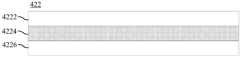
请参阅图5,图5为图4所示偏光组件中电致变色条的结构示意图。电致变色条422可包括层叠设置的变色层4222、电解质层4224和离子存储层4226。Please refer to FIG. 5 . FIG. 5 is a schematic structural diagram of the electrochromic strip in the polarizing assembly shown in FIG. 4 . The
变色层4222是电致变色单元的核心层,也是变色反应的发生层。变色层4222的材料按照类型可分为无机电致变色材料和有机电致变色材料。无机电致变色材料可以是三氧化钨(WO3)或者氧化镍(NiO)。有机电致变色材料主要有聚噻吩类及其衍生物、紫罗精类、四硫富瓦烯、金属酞菁类化合物等。The
电解质层4224由特殊的导电材料组成,如包含有高氯酸锂、高氯酸纳等的溶液的液态电解质材料,或者也可以是固态电解质材料。The
离子存储层4226在电致变色单元中起到存储电荷的作用,即在变色层材料发生氧化还原反应时存储相应的反离子,以保证整个电致变色单元的电荷平衡。The
第二导电层410可以是透明导电层,可以具备导电性和光学透过性。第一导电层480可以是氧化铟锡(ITO),当然第二导电层410也可以为其他材料,诸如氧化锡(SnO2)或氧化锡锑(ATO)。第二导电层420可以铺设在电致变色条420上。第二导电层420可以与多条电致变色条422电性连接,诸如第二导电层420可以与所有的电致变色条422电性连接。The second
第二基层460也可以作为偏光组件400的基体结构。第二基层460可以采用透明材料,诸如无色透明玻璃。第二基层460可以铺设在第二导电层410上。The
当在两个透明导电层(第一导电层480和第二导电层410)之间加上一定的电压时,电致变色条422的变色层4222的材料在电压作用下发生氧化还原反应,从而发生颜色变化。诸如在两个透明导电层(第一导电层480和第二导电层410)之间加上一定的正压可以使得电致变色条422的变色层4222的材料在电压作用下发生着色反应,在两个透明导电层(第一导电层480和第二导电层410)之间加上一定的反压或短路可以使得电致变色条422的变色层4222的材料发声褪色反应。需要说明的是,当施加反压时,该反压的时间不能过长,避免变色层4222的材料再次发声着色反应。When a certain voltage is applied between the two transparent conductive layers (the first
例如,当两个透明导电层(第一导电层480和第二导电层410)为电致变色条422施加的电压由0V变为1V时,电致变色条422可以由无色透明状态变成具有第一颜色的状态。该第一颜色可以为白色、红色或其他颜色。具体请参阅图6,图6为本申请实施例提供的偏光组件具有第一颜色的状态图。For example, when the voltage applied by the two transparent conductive layers (the first
当两个透明导电层(第一导电层480和第二导电层410)为电致变色条422施加的电压由1V变为0V时,电致变色条422可以由具有第一颜色的状态变成无色透明状态。或者当当两个透明导电层(第一导电层480和第二导电层410)短路时,电致变色条422可以由具有第一颜色的状态变成无色透明状态。具体请参阅图7,图7为本申请实施例提供的偏光组件在透明状态下的状态图。其中,该电压值的变化仅为举例说明,其并不构成对电压值变化的限定。When the voltage applied by the two transparent conductive layers (the first
需要说明的是,本申请实施例偏光组件400的结构并不限于此。It should be noted that, the structure of the
请参阅图8,图8为本申请实施例提供的偏光组件的另一结构示意图。偏光组件400可包括第一基层440a、第二基层460a和电致变色层420a。第一基层440a可参阅第一基层440,第二基层460a可以参阅第二基层460,在此不再赘述。Please refer to FIG. 8 , FIG. 8 is another schematic structural diagram of the polarizing assembly provided by the embodiment of the present application. The
电致变色层420a可以包括多个电致变色条422a和多个间隔条424a,多个间隔条424a可以直接由多个无色透明玻璃条通过透明胶粘接在第一基层440a上形成,也可以直接在第一基层440a上开设多个间隔槽形成。多个电致变色条422a和多个间隔条424a间隔设置,即相邻两个电致变色条422a可以由一个间隔条424a间隔开。The
请参阅图9,图9为图8所示偏光组件中电致变色条的结构示意图。电致变色条422a可包括依次层叠设置的第一导电层4228a、离子存储层4226a、电解质层4224a、变色层4222a及第二导电层4221a。第一导电层4228a可以参阅第一导电层480,第一导电层4228a与第一导电层480的区别在于,一个第一导电层4228a对应一个电致变色条422a,第一导电层480对应所有的电致变色条422。至少部分第一导电层4228a电性连接,诸如所有的第一导电层4228a电性连接。Please refer to FIG. 9 . FIG. 9 is a schematic structural diagram of the electrochromic strip in the polarizing assembly shown in FIG. 8 . The
离子存储层4226a可以参阅离子存储层4226,电解质层4224a可以参阅电解质层4224,变色层4222a可以参阅变色层4222,在此不再赘述。The
第二导电层4221a可以参阅第二导电层410,第二导电层4221a与第二导电层410的区别在于,一个第二导电层4221a对应一个电致变色条422a,第二导电层410对应所有的电致变色条422。至少部分第二导电层4221a电性连接,诸如所有的第二导电层4221a电性连接。The second
同样,当在两个透明导电层(第一导电层4228a和第二导电层4221a)之间加上一定的电压时,电致变色条422a的变色层4222a的材料在电压作用下发生氧化还原反应,从而发生颜色变化。诸如在两个透明导电层(第一导电层4228a和第二导电层4221a)之间加上一定的正压可以使得电致变色条422a的变色层4222a的材料在电压作用下发生着色反应,在两个透明导电层(第一导电层4228a和第二导电层4221a)之间加上一定的反压或短路可以使得电致变色条422a的变色层4222a的材料发声褪色反应。当对多条诸如所有的电致变色条422a的两个透明导电层(第一导电层4228a和第二导电层4221a)施加电压时,多条诸如所有的电致变色条422a的状态均会产生变化,具体状态变化可以参阅图6和图7。Similarly, when a certain voltage is applied between the two transparent conductive layers (the first
本申请实施例多条诸如所有的电致变色条422或者电致变色条422a用于在显示面板200的显示状态下显示第一颜色,以使得偏光组件400作为显示面板200的线性偏光片,或者说是光栅。诸如显示装置20在接收到显示指令时,显示装置20的控制器件诸如处理器可以控制显示面板200显示画面以处于显示状态,且该显示装置20的控制器件诸如处理器还控制多条诸如所有的电致变色条422或者电致变色条422a显示第一颜色。多条诸如所有的电致变色条422或者电致变色条422a与多条诸如所有的间隔条424或间隔条424a形成有规律的结构以实现偏光作用,具体请参阅图6。In this embodiment of the present application, a plurality of strips such as all
偏光组件400中电致变色条422或电致变色条422a的宽度可以根据需要设置,相邻两个电致变色条422或电致变色条422a之间的宽度也可以根据需要进行设置,即间隔条424或间隔条424a的宽度可以根据需要进行设置。诸如每毫米宽度可以具有几十至几千条电致变色条422或电致变色条422a,以及几十至几千条间隔条424或间隔条424a。The width of the
再比如:电致变色条422或电致变色条422a的宽度以及间隔条424或间隔条424a的宽度均可以小于见光波长,诸如电致变色条422或电致变色条422a的宽度以及间隔条424或间隔条424a的宽度均小于380nm至780nm(纳米)。Another example: the widths of the
显示面板200在不显示状态时,即显示装置20处于熄屏状态时,显示装置20的控制器件诸如处理器可以控制多条诸如所有的电致变色条422或者电致变色条422a不显示颜色,以使得电致变色条为无色透明状态,从而可以提高显示装置20的透光率。即电致变色条422或者电致变色条422a用于在显示面板200的非显示状态下不显示颜色。当然,显示面板200在在不显示状态时,电致变色条422或者电致变色条422a也可以显示第一颜色。When the
需要说明的是,显示装置20的偏光组件400和显示面板200的配合方式并不限于此,诸如偏光组件400可以仅设置在显示面板200的部分显示区域。It should be noted that the matching manner of the
请参阅图10,图10为本申请实施例提供的显示面板的另一结构示意图。显示面板200a可以应用于显示装置中。该显示面板200a可以包括相互连接的第一显示区220和第二显示区240,本申请实施例可以将偏光组件400和第二线区240层叠设置,而不将偏光组件400铺设到第一显示区220位置,该第一显示区220可以铺设偏光片。可以理解的是,本申请实施例所限定的偏光组件400在电致变色条422或422a处于透明状态时具有高透光率,偏光组件400的透光率远大于偏光片的透光率。因此,可以大大提高第二显示区240位置的透光率。Please refer to FIG. 10 . FIG. 10 is another schematic structural diagram of a display panel provided by an embodiment of the present application. The
第一显示区220的尺寸或者说显示面积可以大于第二显示区240的尺寸或者说显示面积。诸如,第二显示区240设置在第一显示区220的边缘或者说边角位置。第一显示区220可以作为显示装置20的主显示部分,第二显示区240可以作为显示装置20的辅助显示部分,或者说是功能显示部分。当然,第一显示区220的显示面积也可以等于或小于第二显示区240的显示面积。The size or display area of the
本申请实施例可以将第二显示区240的透光率设置大于第一显示区220的透光率。从而在第二显示区240的非显示状态下可以大大提高第二显示区240的透光率,以便于显示装置20在与传感器诸如摄像头等配合时,摄像头可以透过第二显示区240实现信号的传输。需要说明的是,第一显示区220和第二显示区240的尺寸关系并不限于此,诸如第一显示区220和第二显示区240的尺寸相同,再比如,第一显示区220的显示面积小于第二显示区240的显示面积。In this embodiment of the present application, the transmittance of the
为了将第二显示区240的透光率设置大于第一显示区220的透光率,本申请实施例可以将显示装置20中用来驱动第二显示区240的驱动单元诸如薄膜晶体管(TFT)设置在显示装置20的非显示区域,比如设置在显示装置20的侧边或者说是周缘。本申请实施例可以将第二显示区240中像素的排布相比第一显示区220中像素的排布更加稀疏,即第二显示区240中像素的分布密度小于第一显示区220中像素的分布密度,以减少像素、布线及电路。本申请实施例可以将第二显示区240中像素的尺寸设置大于第一显示区220中像素的尺寸,以减少像素、布线及电路。本申请实施例第二显示区240的内部走线可以采用透光材料,诸如氧化铟锡,以提高第二显示区240的透光率。In order to set the light transmittance of the
可以理解的是,以上仅为本申请将第二显示区240的透光率设置大于第一显示区220的透光率的举例说明,本申请实施例将第二显示区240的透光率设置大于第一显示区220的透光率的方式并不局限于此。It can be understood that the above is only an example of setting the light transmittance of the
触控面板600可以包括导电电容触摸传感器电极层或者其他触摸传感器部件(例如,电阻触摸传感器部件、声学触摸传感器部件、基于力的触摸传感器部件、基于光的触摸传感器部件等)。触控面板600可以起到触控的功能。需要说明的是,本申请实施例显示装置20也可以不包括触控面板600。
盖板800可以盖设在触控面板600或偏光组件400上,诸如盖板800盖设在触控面板600上。盖板800可以通过胶层与触控面板600粘接固定。盖板800可以为透明玻璃层、透光塑料、蓝宝石、或其他透明电介质层来保护触控面板600。胶层可以采用透明材料诸如OCA胶。The
本申请实施例显示装置20可以应用于电子设备中。The
请参阅图11,图11为本申请实施例提供的电子设备的结构示意图。电子设备2可以包括显示装置20、壳体40和传感器60。Please refer to FIG. 11 , which is a schematic structural diagram of an electronic device provided by an embodiment of the present application. The electronic device 2 may include a
显示装置20可参阅图1至图9及相关描述,在此不再赘述。显示装置20可以固定在壳体40上,壳体40可由塑料、玻璃、陶瓷、纤维复合材料、金属(例如,不锈钢、铝等)、其他合适的材料、或这些材料的任意两种或更多种的组合形成。壳体40可使用一体式配置形成,在该一体式配置中,一些或全部壳体40被加工或模制成单一结构,或者可使用多个结构(例如,内框架结构、形成外部外壳表面的一种或多种结构等)形成。The
传感器60可以设置在壳体40上,诸如传感器60设置在显示装置20和壳体40之间,传感器60可以透过显示面板200、偏光组件400或偏光组件400a、触控面板600及盖板800传输信号。传感器60也可以仅透过显示面板200、偏光组件400或偏光组件400a及盖板800传输信号。偏光组件400或偏光组件400a可以铺设在显示面板200的整个显示区域,从而显示装置20的各个位置的透光率均有所提升,在显示装置20的下方设置传感器60可以提高传感器60透过显示装置20传输信号的性能。The
比如:电致变色条422或电致变色条422a在显示面板200不显示画面时,可以不显示颜色,从而使得电致变色条422或电致变色条422a为无色透明状态,进而使得偏光组件400整体呈无色透明状态,诸如图7所示的状态。传感器60透过显示面板200和偏光组件400传输信号。For example, the
电子设备2可以通过处理器进行控制,诸如电子设备2的处理器分别与传感器60、显示面板200及偏光组件400或偏光组件400a电性连接,电子设备2的处理器在接收到显示指令时,其可以基于显示指令控制显示面板200处于显示状态,同时还可以控制电致变色条422或电致变色条422a显示第一颜色。此时,电子设备2的处理器可以控制传感器60处于不工作状态。而当电子设备2的处理器接收到传输指令时,电子设备2的处理器可以根据传输指令控制显示面板200处于非显示状态,同时可以控制电致变色条422或电致变色条422a不显示颜色,以及控制传感器60透过显示面板200和偏光组件400或偏光组件400a传输信号。由于偏光组件400或偏光组件400a处于无色透明状态,从而就大大提高传感器60传输信号的质量。The electronic device 2 can be controlled by a processor. For example, the processor of the electronic device 2 is electrically connected to the
其中,传感器60可以包括摄像传感器、指纹传感器、环境光传感器等中的一种或多种。The
需要说明的是,电子设备的显示面板也可以为如图10所示的显示面板。It should be noted that the display panel of the electronic device may also be the display panel shown in FIG. 10 .
请参阅图12,图12为本申请实施例提供的电子设备的另一结构示意图。电子设备2a可以包括显示装置、壳体40和传感器60。其中,壳体40可以参阅图11及相关内容,传感器60可以参阅图11及相关内容,在此不再赘述。Please refer to FIG. 12 , FIG. 12 is another schematic structural diagram of an electronic device provided by an embodiment of the present application. The
显示装置可以包括显示面板200a和偏光组件,显示面板200a可以参阅图10及相关内容,偏光组件可以参阅图2至9及相关内容,即偏光组件可以是偏光组件400,也可以是偏光组件400a。The display device may include a
本申请实施例传感器60可以透过第二显示区240传输信号。电子设备2a可以通过处理器进行控制,诸如电子设备2的处理器分别与传感器60、显示面板200a及偏光组件400或偏光组件400a电性连接,电子设备2a的处理器在接收到显示指令时,其可以基于显示指令控制显示面板200a处于显示状态,同时还可以控制电致变色条422或电致变色条422a显示第一颜色。此时,电子设备2a的处理器可以控制传感器60处于不工作状态。而当电子设备2a的处理器接收到传输指令时,处理器可以根据传输指令控制显示面板200a处于非显示状态,同时可以控制电致变色条422或电致变色条422a不显示颜色,以及控制传感器60透过第二显示区240和偏光组件400或偏光组件400a传输信号。由于偏光组件400或偏光组件400a处于无色透明状态,从而就大大提高传感器60传输信号的质量。The
以上对本申请实施例提供的显示装置和电子设备进行了详细介绍。本文中应用了具体个例对本申请的原理及实施方式进行了阐述,以上实施例的说明只是用于帮助理解本申请。同时,对于本领域的技术人员,依据本申请的思想,在具体实施方式及应用范围上均会有改变之处,综上所述,本说明书内容不应理解为对本申请的限制。The display device and the electronic device provided by the embodiments of the present application have been described in detail above. The principles and implementations of the present application are described herein by using specific examples, and the descriptions of the above embodiments are only used to help the understanding of the present application. At the same time, for those skilled in the art, according to the idea of the present application, there will be changes in the specific embodiments and application scope. To sum up, the content of this specification should not be construed as a limitation to the present application.
Claims (18)
Priority Applications (2)
| Application Number | Priority Date | Filing Date | Title |
|---|---|---|---|
| CN201911049442.4ACN110751900B (en) | 2019-10-31 | 2019-10-31 | Display devices and electronic equipment |
| PCT/CN2020/116476WO2021082804A1 (en) | 2019-10-31 | 2020-09-21 | Display device and electronic apparatus |
Applications Claiming Priority (1)
| Application Number | Priority Date | Filing Date | Title |
|---|---|---|---|
| CN201911049442.4ACN110751900B (en) | 2019-10-31 | 2019-10-31 | Display devices and electronic equipment |
Publications (2)
| Publication Number | Publication Date |
|---|---|
| CN110751900Atrue CN110751900A (en) | 2020-02-04 |
| CN110751900B CN110751900B (en) | 2022-03-01 |
Family
ID=69281385
Family Applications (1)
| Application Number | Title | Priority Date | Filing Date |
|---|---|---|---|
| CN201911049442.4AActiveCN110751900B (en) | 2019-10-31 | 2019-10-31 | Display devices and electronic equipment |
Country Status (2)
| Country | Link |
|---|---|
| CN (1) | CN110751900B (en) |
| WO (1) | WO2021082804A1 (en) |
Cited By (8)
| Publication number | Priority date | Publication date | Assignee | Title |
|---|---|---|---|---|
| CN111624806A (en)* | 2020-05-29 | 2020-09-04 | 厦门天马微电子有限公司 | Display module and display device |
| CN111863920A (en)* | 2020-07-29 | 2020-10-30 | 京东方科技集团股份有限公司 | Display panel and display device |
| CN112198707A (en)* | 2020-11-20 | 2021-01-08 | 厦门天马微电子有限公司 | Display panel and display device |
| CN112434605A (en)* | 2020-11-24 | 2021-03-02 | 合肥维信诺科技有限公司 | Display device |
| WO2021082804A1 (en)* | 2019-10-31 | 2021-05-06 | Oppo广东移动通信有限公司 | Display device and electronic apparatus |
| CN114002889A (en)* | 2020-07-17 | 2022-02-01 | 深圳市万普拉斯科技有限公司 | Polarization cover plate of camera and electronic equipment |
| CN114879404A (en)* | 2021-02-05 | 2022-08-09 | 北京京东方显示技术有限公司 | Liquid crystal display and display device |
| US12201004B2 (en) | 2019-04-23 | 2025-01-14 | Apple Inc. | Methods and configurations for improving the performance of sensors under a display |
Citations (11)
| Publication number | Priority date | Publication date | Assignee | Title |
|---|---|---|---|---|
| KR20090042099A (en)* | 2007-10-25 | 2009-04-29 | 미래나노텍(주) | Nano wire grid polarizer unit and its manufacturing method |
| CN100524891C (en)* | 2002-03-26 | 2009-08-05 | 夏普株式会社 | Organic EL light emitting device and liquid crystal display using the same |
| CN104122671A (en)* | 2014-07-10 | 2014-10-29 | 京东方科技集团股份有限公司 | Three-dimensional display device |
| CN104468882A (en)* | 2013-09-18 | 2015-03-25 | 宏达国际电子股份有限公司 | Portable electronic device |
| CN104834146A (en)* | 2015-05-25 | 2015-08-12 | 京东方科技集团股份有限公司 | Display instrument, manufacturing method and driving method of display instrument and display device |
| CN106098737A (en)* | 2016-07-05 | 2016-11-09 | 京东方科技集团股份有限公司 | A kind of organic LED display panel and preparation method thereof and display device |
| CN106292017A (en)* | 2015-06-05 | 2017-01-04 | 中兴通讯股份有限公司 | A kind of arrangement for deflecting, intelligent terminal and intelligent terminal's method to set up, display packing |
| CN107507854A (en)* | 2017-09-13 | 2017-12-22 | 昆山维信诺科技有限公司 | Oled display panel |
| CN107943211A (en)* | 2017-11-30 | 2018-04-20 | 维沃移动通信有限公司 | terminal device and its control method |
| CN208819534U (en)* | 2019-03-28 | 2019-05-03 | 北京小米移动软件有限公司 | a terminal |
| CN110320723A (en)* | 2018-03-28 | 2019-10-11 | 京东方科技集团股份有限公司 | Display device and its display methods, display equipment |
Family Cites Families (10)
| Publication number | Priority date | Publication date | Assignee | Title |
|---|---|---|---|---|
| KR20080058722A (en)* | 2006-12-22 | 2008-06-26 | 서울옵토디바이스주식회사 | A light emitting device manufacturing method comprising a scattering center having a plurality of insulating layers stacked thereon and the light emitting device |
| KR101337616B1 (en)* | 2006-12-28 | 2013-12-06 | 서울바이오시스 주식회사 | Fabrication method of light emitting device having scattering center laminated with a plurality of insulator layer and light emitting device thereby |
| CN102540607A (en)* | 2010-12-07 | 2012-07-04 | 介面光电股份有限公司 | Electrochromic module of organic and inorganic materials and display device incorporating the same |
| US9442339B2 (en)* | 2010-12-08 | 2016-09-13 | View, Inc. | Spacers and connectors for insulated glass units |
| TWI514621B (en)* | 2013-06-14 | 2015-12-21 | Lextar Electronics Corp | Light-emitting diode structure |
| CN104749850B (en)* | 2015-04-17 | 2017-11-07 | 京东方科技集团股份有限公司 | Electrochromic display panel and its driving method, display device |
| CN109116613B (en)* | 2017-06-26 | 2020-11-24 | 京东方科技集团股份有限公司 | Display device and operation method thereof |
| CN108681171A (en)* | 2018-05-23 | 2018-10-19 | 广州奥翼电子科技股份有限公司 | Optical element, display device and electronic equipment |
| CN108983525A (en)* | 2018-08-14 | 2018-12-11 | Oppo广东移动通信有限公司 | Electrochromic components and electronic devices |
| CN110751900B (en)* | 2019-10-31 | 2022-03-01 | Oppo广东移动通信有限公司 | Display devices and electronic equipment |
- 2019
- 2019-10-31CNCN201911049442.4Apatent/CN110751900B/enactiveActive
- 2020
- 2020-09-21WOPCT/CN2020/116476patent/WO2021082804A1/ennot_activeCeased
Patent Citations (11)
| Publication number | Priority date | Publication date | Assignee | Title |
|---|---|---|---|---|
| CN100524891C (en)* | 2002-03-26 | 2009-08-05 | 夏普株式会社 | Organic EL light emitting device and liquid crystal display using the same |
| KR20090042099A (en)* | 2007-10-25 | 2009-04-29 | 미래나노텍(주) | Nano wire grid polarizer unit and its manufacturing method |
| CN104468882A (en)* | 2013-09-18 | 2015-03-25 | 宏达国际电子股份有限公司 | Portable electronic device |
| CN104122671A (en)* | 2014-07-10 | 2014-10-29 | 京东方科技集团股份有限公司 | Three-dimensional display device |
| CN104834146A (en)* | 2015-05-25 | 2015-08-12 | 京东方科技集团股份有限公司 | Display instrument, manufacturing method and driving method of display instrument and display device |
| CN106292017A (en)* | 2015-06-05 | 2017-01-04 | 中兴通讯股份有限公司 | A kind of arrangement for deflecting, intelligent terminal and intelligent terminal's method to set up, display packing |
| CN106098737A (en)* | 2016-07-05 | 2016-11-09 | 京东方科技集团股份有限公司 | A kind of organic LED display panel and preparation method thereof and display device |
| CN107507854A (en)* | 2017-09-13 | 2017-12-22 | 昆山维信诺科技有限公司 | Oled display panel |
| CN107943211A (en)* | 2017-11-30 | 2018-04-20 | 维沃移动通信有限公司 | terminal device and its control method |
| CN110320723A (en)* | 2018-03-28 | 2019-10-11 | 京东方科技集团股份有限公司 | Display device and its display methods, display equipment |
| CN208819534U (en)* | 2019-03-28 | 2019-05-03 | 北京小米移动软件有限公司 | a terminal |
Cited By (11)
| Publication number | Priority date | Publication date | Assignee | Title |
|---|---|---|---|---|
| US12201004B2 (en) | 2019-04-23 | 2025-01-14 | Apple Inc. | Methods and configurations for improving the performance of sensors under a display |
| WO2021082804A1 (en)* | 2019-10-31 | 2021-05-06 | Oppo广东移动通信有限公司 | Display device and electronic apparatus |
| CN111624806A (en)* | 2020-05-29 | 2020-09-04 | 厦门天马微电子有限公司 | Display module and display device |
| CN111624806B (en)* | 2020-05-29 | 2022-09-23 | 厦门天马微电子有限公司 | Display module and display device |
| CN114002889A (en)* | 2020-07-17 | 2022-02-01 | 深圳市万普拉斯科技有限公司 | Polarization cover plate of camera and electronic equipment |
| CN111863920A (en)* | 2020-07-29 | 2020-10-30 | 京东方科技集团股份有限公司 | Display panel and display device |
| CN111863920B (en)* | 2020-07-29 | 2023-12-12 | 京东方科技集团股份有限公司 | Display panel and display device |
| CN112198707A (en)* | 2020-11-20 | 2021-01-08 | 厦门天马微电子有限公司 | Display panel and display device |
| CN112434605A (en)* | 2020-11-24 | 2021-03-02 | 合肥维信诺科技有限公司 | Display device |
| CN112434605B (en)* | 2020-11-24 | 2023-12-01 | 合肥维信诺科技有限公司 | Display device |
| CN114879404A (en)* | 2021-02-05 | 2022-08-09 | 北京京东方显示技术有限公司 | Liquid crystal display and display device |
Also Published As
| Publication number | Publication date |
|---|---|
| WO2021082804A1 (en) | 2021-05-06 |
| CN110751900B (en) | 2022-03-01 |
Similar Documents
| Publication | Publication Date | Title |
|---|---|---|
| CN110751900B (en) | Display devices and electronic equipment | |
| CN104730719B (en) | Touch-control bore hole grating 3D display devices and its preparation and control method | |
| TWI730411B (en) | Electrochromic display device and driving method thereof | |
| CN106526951B (en) | Mirror display device and control method thereof | |
| CN102646696B (en) | Organic light-emitting diode display device, manufacturing method thereof and display system | |
| US9383850B2 (en) | Touch screen and manufacturing method | |
| KR102416142B1 (en) | Back cover and transparent display apparatus using the same | |
| CN104216578A (en) | Touch panel and display device | |
| CN103488341A (en) | In-cell touch panel and display device | |
| CN111965864B (en) | Dimming structure and display device | |
| CN109542273B (en) | Display panel and display device | |
| US20210202619A1 (en) | Light source panel and display device | |
| CN110783482A (en) | Display panel and its manufacturing method, display screen and display device | |
| TW201617804A (en) | Touch substrate | |
| JP2016021170A (en) | Display device with electrostatic capacitance coupling method touch panel input device | |
| TWI422905B (en) | Touch panel integrated in display | |
| CN103698926B (en) | A kind of display device and preparation method thereof | |
| CN102819154B (en) | Liquid crystal panel and display device | |
| CN112198707A (en) | Display panel and display device | |
| KR101206285B1 (en) | Display device capable of adjusting viewing angle and fabrication method the same | |
| CN107608565B (en) | Touch display panel and touch display device | |
| KR101931618B1 (en) | Reflective display device | |
| CN206057760U (en) | A kind of liquid crystal grating, 3D display floaters and display device | |
| KR102522531B1 (en) | Mirror display panel | |
| KR100350536B1 (en) | Liquid crystal display device having a polarizer |
Legal Events
| Date | Code | Title | Description |
|---|---|---|---|
| PB01 | Publication | ||
| PB01 | Publication | ||
| SE01 | Entry into force of request for substantive examination | ||
| SE01 | Entry into force of request for substantive examination | ||
| GR01 | Patent grant | ||
| GR01 | Patent grant |