CN110710058A - Multipin Connector Plug Block Assembly - Google Patents
Multipin Connector Plug Block AssemblyDownload PDFInfo
- Publication number
- CN110710058A CN110710058ACN201880037237.3ACN201880037237ACN110710058ACN 110710058 ACN110710058 ACN 110710058ACN 201880037237 ACN201880037237 ACN 201880037237ACN 110710058 ACN110710058 ACN 110710058A
- Authority
- CN
- China
- Prior art keywords
- pin
- connector plug
- plug block
- connector
- block assembly
- Prior art date
- Legal status (The legal status is an assumption and is not a legal conclusion. Google has not performed a legal analysis and makes no representation as to the accuracy of the status listed.)
- Granted
Links
Images


Classifications
- H—ELECTRICITY
- H01—ELECTRIC ELEMENTS
- H01R—ELECTRICALLY-CONDUCTIVE CONNECTIONS; STRUCTURAL ASSOCIATIONS OF A PLURALITY OF MUTUALLY-INSULATED ELECTRICAL CONNECTING ELEMENTS; COUPLING DEVICES; CURRENT COLLECTORS
- H01R9/00—Structural associations of a plurality of mutually-insulated electrical connecting elements, e.g. terminal strips or terminal blocks; Terminals or binding posts mounted upon a base or in a case; Bases therefor
- H01R9/22—Bases, e.g. strip, block, panel
- H01R9/24—Terminal blocks
- H01R9/26—Clip-on terminal blocks for side-by-side rail- or strip-mounting
- H—ELECTRICITY
- H01—ELECTRIC ELEMENTS
- H01R—ELECTRICALLY-CONDUCTIVE CONNECTIONS; STRUCTURAL ASSOCIATIONS OF A PLURALITY OF MUTUALLY-INSULATED ELECTRICAL CONNECTING ELEMENTS; COUPLING DEVICES; CURRENT COLLECTORS
- H01R12/00—Structural associations of a plurality of mutually-insulated electrical connecting elements, specially adapted for printed circuits, e.g. printed circuit boards [PCB], flat or ribbon cables, or like generally planar structures, e.g. terminal strips, terminal blocks; Coupling devices specially adapted for printed circuits, flat or ribbon cables, or like generally planar structures; Terminals specially adapted for contact with, or insertion into, printed circuits, flat or ribbon cables, or like generally planar structures
- H01R12/50—Fixed connections
- H01R12/51—Fixed connections for rigid printed circuits or like structures
- H01R12/55—Fixed connections for rigid printed circuits or like structures characterised by the terminals
- H01R12/57—Fixed connections for rigid printed circuits or like structures characterised by the terminals surface mounting terminals
- H—ELECTRICITY
- H01—ELECTRIC ELEMENTS
- H01R—ELECTRICALLY-CONDUCTIVE CONNECTIONS; STRUCTURAL ASSOCIATIONS OF A PLURALITY OF MUTUALLY-INSULATED ELECTRICAL CONNECTING ELEMENTS; COUPLING DEVICES; CURRENT COLLECTORS
- H01R12/00—Structural associations of a plurality of mutually-insulated electrical connecting elements, specially adapted for printed circuits, e.g. printed circuit boards [PCB], flat or ribbon cables, or like generally planar structures, e.g. terminal strips, terminal blocks; Coupling devices specially adapted for printed circuits, flat or ribbon cables, or like generally planar structures; Terminals specially adapted for contact with, or insertion into, printed circuits, flat or ribbon cables, or like generally planar structures
- H01R12/70—Coupling devices
- H01R12/71—Coupling devices for rigid printing circuits or like structures
- H01R12/712—Coupling devices for rigid printing circuits or like structures co-operating with the surface of the printed circuit or with a coupling device exclusively provided on the surface of the printed circuit
- H01R12/714—Coupling devices for rigid printing circuits or like structures co-operating with the surface of the printed circuit or with a coupling device exclusively provided on the surface of the printed circuit with contacts abutting directly the printed circuit; Button contacts therefore provided on the printed circuit
- H—ELECTRICITY
- H01—ELECTRIC ELEMENTS
- H01R—ELECTRICALLY-CONDUCTIVE CONNECTIONS; STRUCTURAL ASSOCIATIONS OF A PLURALITY OF MUTUALLY-INSULATED ELECTRICAL CONNECTING ELEMENTS; COUPLING DEVICES; CURRENT COLLECTORS
- H01R12/00—Structural associations of a plurality of mutually-insulated electrical connecting elements, specially adapted for printed circuits, e.g. printed circuit boards [PCB], flat or ribbon cables, or like generally planar structures, e.g. terminal strips, terminal blocks; Coupling devices specially adapted for printed circuits, flat or ribbon cables, or like generally planar structures; Terminals specially adapted for contact with, or insertion into, printed circuits, flat or ribbon cables, or like generally planar structures
- H01R12/70—Coupling devices
- H01R12/91—Coupling devices allowing relative movement between coupling parts, e.g. floating or self aligning
- H—ELECTRICITY
- H01—ELECTRIC ELEMENTS
- H01R—ELECTRICALLY-CONDUCTIVE CONNECTIONS; STRUCTURAL ASSOCIATIONS OF A PLURALITY OF MUTUALLY-INSULATED ELECTRICAL CONNECTING ELEMENTS; COUPLING DEVICES; CURRENT COLLECTORS
- H01R13/00—Details of coupling devices of the kinds covered by groups H01R12/70 or H01R24/00 - H01R33/00
- H01R13/646—Details of coupling devices of the kinds covered by groups H01R12/70 or H01R24/00 - H01R33/00 specially adapted for high-frequency, e.g. structures providing an impedance match or phase match
- H—ELECTRICITY
- H01—ELECTRIC ELEMENTS
- H01R—ELECTRICALLY-CONDUCTIVE CONNECTIONS; STRUCTURAL ASSOCIATIONS OF A PLURALITY OF MUTUALLY-INSULATED ELECTRICAL CONNECTING ELEMENTS; COUPLING DEVICES; CURRENT COLLECTORS
- H01R9/00—Structural associations of a plurality of mutually-insulated electrical connecting elements, e.g. terminal strips or terminal blocks; Terminals or binding posts mounted upon a base or in a case; Bases therefor
- H01R9/22—Bases, e.g. strip, block, panel
- H01R9/24—Terminal blocks
- H01R9/26—Clip-on terminal blocks for side-by-side rail- or strip-mounting
- H01R9/2691—Clip-on terminal blocks for side-by-side rail- or strip-mounting with ground wire connection to the rail
- H—ELECTRICITY
- H01—ELECTRIC ELEMENTS
- H01R—ELECTRICALLY-CONDUCTIVE CONNECTIONS; STRUCTURAL ASSOCIATIONS OF A PLURALITY OF MUTUALLY-INSULATED ELECTRICAL CONNECTING ELEMENTS; COUPLING DEVICES; CURRENT COLLECTORS
- H01R13/00—Details of coupling devices of the kinds covered by groups H01R12/70 or H01R24/00 - H01R33/00
- H01R13/46—Bases; Cases
- H01R13/502—Bases; Cases composed of different pieces
- H01R13/504—Bases; Cases composed of different pieces different pieces being moulded, cemented, welded, e.g. ultrasonic, or swaged together
- H01R13/5045—Bases; Cases composed of different pieces different pieces being moulded, cemented, welded, e.g. ultrasonic, or swaged together different pieces being assembled by press-fit
- H—ELECTRICITY
- H01—ELECTRIC ELEMENTS
- H01R—ELECTRICALLY-CONDUCTIVE CONNECTIONS; STRUCTURAL ASSOCIATIONS OF A PLURALITY OF MUTUALLY-INSULATED ELECTRICAL CONNECTING ELEMENTS; COUPLING DEVICES; CURRENT COLLECTORS
- H01R24/00—Two-part coupling devices, or either of their cooperating parts, characterised by their overall structure
- H01R24/38—Two-part coupling devices, or either of their cooperating parts, characterised by their overall structure having concentrically or coaxially arranged contacts
- H01R24/40—Two-part coupling devices, or either of their cooperating parts, characterised by their overall structure having concentrically or coaxially arranged contacts specially adapted for high frequency
- H01R24/50—Two-part coupling devices, or either of their cooperating parts, characterised by their overall structure having concentrically or coaxially arranged contacts specially adapted for high frequency mounted on a PCB [Printed Circuit Board]
Landscapes
- Details Of Connecting Devices For Male And Female Coupling (AREA)
- Coupling Device And Connection With Printed Circuit (AREA)
Abstract
Translated fromChineseDescription
Translated fromChinese技术领域technical field
此申请案主张于2017年4月28日所提出的第15/581913号美国申请案的优先权权益,所述美国申请案以引用方式并入本文中。This application claims the benefit of priority from US Application No. 15/581913, filed April 28, 2017, which is incorporated herein by reference.
本公开案通常涉及多针脚连接器插头块组件,且特别是涉及具有多个RF连接器针脚组件的多针脚连接器插头块组件,各个RF连接器针脚组件具有浮动的接脚(也称为“连接器针脚”),所述浮动接触针脚安装在安置于所述RF连接器针脚组件中的外壳中以供连接到印刷电路板。The present disclosure relates generally to multi-pin connector block assemblies, and in particular to multi-pin connector block assemblies having multiple RF connector pin assemblies, each RF connector pin assembly having floating pins (also referred to as "" connector pins"), the floating contact pins are mounted in a housing disposed in the RF connector pin assembly for connection to a printed circuit board.
背景技术Background technique
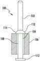
在微波频率连接器的技术领域内,存在着被设计为软焊到印刷电路板(PCB)上的公接脚。这些接脚是金属的,且一般被塑料绝缘体和提供连接器针脚组件的金属外壳围绕。可通过各种方法(包括推装式设计(push-on design))来耦接连接器针脚组件。接脚在电讯号的传输上是关键元件。存在着由于容差迭加和不扁平的PCB,连接器需要克服大的可变距离且仍在高频下维持良好性能的实例。据此,已将努力聚焦在研发并入所谓的“浮动”接脚的连接器针脚组件上,所述浮动接脚双向地轴向移动以适应PCB的表面平坦度的不均匀性。然而,需要将接脚的轴向移动约束在两个方向上以允许将接脚保留在载体或头座中;且为了工作,约束器必须在直径上大于载体或头座中的通路的内径。连接器针脚组件的组装上的困难涉及在约束器大于通路时将具有两个约束器的接脚安插通过通路,和在不损伤载体或头座的情况下如此做。这在使用并入多个接脚的连接器针脚组件的情况下是特别困难的。In the technical field of microwave frequency connectors, there are male pins designed to be soldered onto a printed circuit board (PCB). These pins are metal and are typically surrounded by a plastic insulator and a metal housing that provides the connector pin assembly. Connector pin assemblies may be coupled by various methods, including push-on designs. Pins are key components in the transmission of electrical signals. There are instances where connectors need to overcome large variable distances and still maintain good performance at high frequencies due to stacked tolerances and non-flat PCBs. Accordingly, efforts have been focused on developing connector pin assemblies that incorporate so-called "floating" pins that move axially bidirectionally to accommodate non-uniformities in the surface flatness of the PCB. However, axial movement of the pins needs to be constrained in both directions to allow the pins to remain in the carrier or header; and in order to work, the restraint must be larger in diameter than the inner diameter of the passage in the carrier or header. A difficulty in the assembly of the connector pin assembly involves inserting a pin with two restraints through the passage when the restraint is larger than the passage, and doing so without damaging the carrier or header. This is particularly difficult when using connector pin assemblies that incorporate multiple pins.
参照图1和图2,绘示了常规的浮动针脚组件100。图1中示出了单个针脚布置,而图2中示出了多针脚布置。在图1和图2中,各个针脚102被示为安装通过载体106中的孔洞104。针脚102一般是由导电材料(例如金属)制造的,而载体106一般是由电介材料制造的,使得载体106可充当针脚102的绝缘体。载体106也可称为头座。为了允许针脚102“浮动”,针脚102具有轴杆108,所述轴杆具有较孔洞104的内径为小的外径。如此,轴杆108可在孔洞104中自由滑动,从而允许针脚102轴向移动。然而,限制针脚102的双向轴向移动的量以将针脚102维持在载体106内是必要的。为了提供此类双向限制,针脚102具有两个整体式约束器(用来在第一方向上限制针脚102的轴向移动的第一约束器110和用来在第二方向上限制针脚102的轴向移动的第二约束器112)。1 and 2, a conventional
第一约束器110和第二约束器112从轴杆108的表面向外径向延伸。然而,为了能够限制针脚102的轴向移动,第一约束器110和第二约束器112两者必须从轴杆108向外径向延伸到孔洞104的外径以外的周边周缘。一般而言,第一约束器110和第二约束器112两者是与针脚102单块地一同形成的且被形成为所述针脚的一部分。因为针脚102的必要尺寸和单块结构,第一约束器110或第二约束器112中的一个必须通过在组装浮动针脚组件100的期间强迫所述约束器通过孔洞104来安插在载体106中。据此,第一约束器110和第二约束器112中的一个或两个可具有圆头的或倾斜的边缘或表面以促进此类安插行为。如图1和图2中可见的,第一约束器110具有倾斜面114,指示曾通过强迫第一约束器110通过孔洞104来将针脚102安插在载体106中。虽然倾斜面114可促进针脚102的安装到某个程度,但此类安装行为在载体106的材料上施加了应力,这可能造成破裂或在实体上危害载体106和/或危害其绝缘整体性的某种其他结构损害。此外,倾斜面114仅允许在一个方向上安装针脚102。The
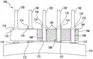
此类结构冲击和危害效应的机会在如图2中所绘示的多针脚布置的情况下更加恶化。图2中示出了五个针脚102,且可能已经通过强迫各别第一约束器110通过载体106中的各别孔洞104来安装了各个针脚。虽然针脚102可在孔洞104中双向轴向移动,此类移动仅发生在第一约束器110和第二约束器112之间。如此,一旦被安装,可能不能通过持续在与所安装的相同方向上强迫针脚102或通过将所述针脚强迫回来通过孔洞104来移除针脚102。据此,一旦针脚102中的一个被安装在载体106中,则不能在不损伤载体106的情况下移动所述针脚。The chances of such structural shock and hazard effects are exacerbated with a multi-pin arrangement as depicted in FIG. 2 . Five
在图2中,第二约束器112被示为与印刷电路板(PCB)116接合。在这方面,各个针脚102上的第二约束器112还被用作要连接到PCB 116的接头,且可被软焊到PCB 116上的导电轨迹(未示于图2中)。PCB 116可能不是完美扁平或平坦的且可能具有表面不均匀性,举例而言,例如如图2中针对PCB116所绘示的弓弧。在不同的第二约束器112接合PCB 116时,PCB116的表面中的不均匀性使得第二约束器112移动,这轴向地移动了针脚102,而允许针脚102“浮动”。然而,因为第二约束器112也被用作接头,PCB 116的不均匀性可能使得第二约束器112被强迫抵着载体106。这在图2中由安装在中间的针脚102所示。此安装行为不仅增加损伤载体106的可能性,且还可能危害第二约束器112到PCB 116上的导电轨迹的连接的整体性。In FIG. 2 , the
从而,存在着一种射频(RF)连接器针脚组件的未解决需要,所述射频连接器针脚组件不仅提供了轴向移动或浮动的针脚以适应PCB表面的不均匀性,且还可在不危害载体或头座或通往PCB的连接的情况下被安装。Thus, there is an unsolved need for a radio frequency (RF) connector pin assembly that not only provides pins that move axially or float to accommodate PCB surface non-uniformities, but also Installed without jeopardizing the carrier or header or connections to the PCB.
并不承认本文中所援引的任何参考文献构成了现有技术。申请人明确地保留挑战任何所援引的文件的正确性和恰当性的权利。There is no admission that any of the references cited herein constitute prior art. Applicants expressly reserve the right to challenge the correctness and propriety of any cited document.
发明内容SUMMARY OF THE INVENTION
本公开案的一个实施方式关于一种射频(RF)连接器插头块组件。所述RF连接器插头块组件包括:多连接器插头块,包括多个外壳端口,其中所述多连接器插头块可附接到外部结构。所述RF连接器插头块组件还包括:多个外壳,其中所述多个外壳中的各个外壳可移除地安装在所述多个外壳端口中的一外壳端口中,且其中所述多个外壳中的一外壳相对于所述多个外壳中的另一外壳被可独立移除地安装。所述RF连接器插头块组件还包括:接脚,可移动地安置在所述多个外壳中的各个外壳中,其中所述多个外壳中的一个外壳中的所述接脚相对于所述多个外壳中的另一外壳中的所述接脚在第一方向和第二方向上可独立轴向移动。One embodiment of the present disclosure relates to a radio frequency (RF) connector plug block assembly. The RF connector plug block assembly includes a multi-connector plug block including a plurality of housing ports, wherein the multi-connector plug block is attachable to an external structure. The RF connector plug block assembly further includes a plurality of housings, wherein each housing of the plurality of housings is removably mounted in a housing port of the plurality of housing ports, and wherein the plurality of housings One of the housings is independently removably mounted relative to the other of the plurality of housings. The RF connector plug block assembly further includes pins removably seated in each of the plurality of housings, wherein the pins in one of the plurality of housings are relative to the The pins in another of the plurality of housings are independently axially movable in a first direction and a second direction.
本公开案的另一实施方式涉及一种RF连接器插头块组件。所述RF连接器插头块组件包括:连接器插头块,包括至少一个外壳端口,其中所述连接器插头块可附接到外部结构。所述RF连接器插头块组件还包括:至少一个外壳,可移除地安装在所述至少一个外壳端口中。所述RF连接器插头块组件还包括:至少一个接脚,可移动地安置在所述至少一个外壳中,其中所述至少一个外壳中的所述至少一个接脚在第一方向和第二方向上可移动。Another embodiment of the present disclosure relates to an RF connector plug block assembly. The RF connector plug block assembly includes a connector plug block including at least one housing port, wherein the connector plug block is attachable to an external structure. The RF connector plug block assembly also includes at least one housing removably mountable in the at least one housing port. The RF connector plug block assembly further includes: at least one pin removably seated in the at least one housing, wherein the at least one pin in the at least one housing is in a first direction and a second direction can be moved up.
本公开案的另一实施方式涉及一种RF连接器针脚组件。RF连接器针脚组件包括第一电介体,所述第一电介体包括第一止动面和延伸通过第一电介体的第一穿通路。RF连接器针脚组件还包括第二电介体,所述第二电介体包括与第一止动面相对地定位的第二止动面和延伸通过第二电介体的第二穿通路,其中第二穿通路与第一穿通路对准,且其中第一止动面和第二止动面界定第一电介体和第二电介体之间的间隙。RF连接器针脚组件还包括接脚,所述接脚包括第一针脚区段、第二针脚区段和第一针脚区段和第二针脚区段的接合点处的环形端箍。第一针脚区段可移动地安置在第一穿通路中,而第二针脚区段可移动地安置在第二穿通路中。环形端箍定位在间隙中。接脚的轴向移动受限于第一止动面和第二止动面之间的间隙中的环形端箍的移动。第一针脚区段被调适为提供与外部元件的电气连续性,而第二针脚区段在远侧上终结于连接特征中。Another embodiment of the present disclosure relates to an RF connector pin assembly. The RF connector pin assembly includes a first dielectric body including a first stop surface and a first through-hole extending through the first dielectric body. The RF connector pin assembly also includes a second dielectric body including a second stop surface positioned opposite the first stop surface and a second through passage extending through the second dielectric body, wherein the second via is aligned with the first via, and wherein the first stop surface and the second stop surface define a gap between the first dielectric body and the second dielectric body. The RF connector pin assembly also includes pins that include a first pin segment, a second pin segment, and an annular end cuff at a junction of the first pin segment and the second pin segment. The first stitch section is movably arranged in the first passage, and the second stitch section is movably arranged in the second passage. The annular end cuff is positioned in the gap. Axial movement of the pins is limited by movement of the annular end cuff in the gap between the first and second stop surfaces. The first stitch section is adapted to provide electrical continuity with the external element, while the second stitch section terminates distally in the connection feature.
本公开案的另一实施方式涉及一种RF连接器针脚组件。所述RF连接器针脚组件包括:外壳,包括第一节段和通过间壁与所述第一节段分离的第二节段。所述间壁包括延伸于所述第一节段和所述第二节段之间的一出入口。所述RF连接器针脚组件还包括:第一电介体,定位在所述第二节段中。所述第一电介体包括第一止动面和延伸通过所述第一电介体的第一穿通路,其中所述第一穿通路与所述出入口对准。所述RF连接器针脚组件还包括:第二电介体,定位在所述第二节段中。所述第二电介体包括与所述第一止动面相对地定位的第二止动面和延伸通过所述第二电介体的第二穿通路。所述第二穿通路与所述第一穿通路和与所述出入口对准,且所述第一止动面和所述第二止动面界定所述第一电介体和所述第二电介体之间的间隙。第一止动面通过所述间隙与第二止动面分隔一距离“A”。RF连接器针脚组件还包括接脚,所述接脚包括第一针脚区段、第二针脚区段和第一针脚区段与第二针脚区段的接合点处的环形端箍。第一针脚区段可移动地安置在第一穿通路中,而第二针脚区段可移动地安置在第二穿通路中。所述接脚在所述第一穿通路和所述第二穿通路中在第一方向和第二方向上可轴向移动,且所述环形端箍定位在所述间隙中。所述接脚的轴向移动被所述第一止动面限制于所述间隙中的所述环形端箍在所述第一方向上的移动,且被所述第二止动面限制于所述间隙中的所述环形端箍在所述第二方向上的移动。所述第一针脚区段延伸通过所述第一穿通路且通过所述出入口进入所述第一节段,且所述第二针脚区段在远侧上终结于连接特征中。Another embodiment of the present disclosure relates to an RF connector pin assembly. The RF connector pin assembly includes a housing including a first segment and a second segment separated from the first segment by a partition wall. The partition includes an access port extending between the first segment and the second segment. The RF connector pin assembly also includes a first dielectric positioned in the second segment. The first dielectric body includes a first stop surface and a first through passage extending through the first dielectric body, wherein the first through passage is aligned with the port. The RF connector pin assembly also includes a second dielectric positioned in the second segment. The second dielectric body includes a second stop surface positioned opposite the first stop surface and a second through passage extending through the second dielectric body. The second through-passage is aligned with the first through-passage and with the port, and the first and second stop surfaces define the first dielectric and the second gap between the dielectrics. The first stop surface is separated from the second stop surface by a distance "A" through the gap. The RF connector pin assembly also includes a pin including a first pin segment, a second pin segment, and an annular end cuff at a junction of the first pin segment and the second pin segment. The first stitch section is movably arranged in the first passage, and the second stitch section is movably arranged in the second passage. The pins are axially movable in first and second directions in the first and second passages, and the annular end cuff is positioned in the gap. The axial movement of the pin is limited by the first stop surface to the movement of the annular end cuff in the gap in the first direction, and is limited to the second stop surface by the second stop surface. movement of the annular end cuff in the gap in the second direction. The first stitch segment extends through the first pass-through and into the first segment through the access port, and the second stitch segment terminates distally in a connecting feature.
本公开案的另一实施方式涉及一种RF连接器针脚组件。所述RF连接器针脚组件包括:外壳,包括第一节段和通过一间壁与所述第一节段分离的第二节段。所述间壁包括延伸于所述第一节段和所述第二节段之间的出入口。所述RF连接器针脚组件更包括:电介体,定位在所述第二节段中。所述电介体包括延伸通过第一面和一第二面之间的所述电介体的穿通路,且其中所述穿通路包括内径“TPID”且与所述出入口对准。所述RF连接器针脚组件更包括:接脚,包括具有第一端和第二端的轴杆。所述轴杆可移动地摩擦契合在所述穿通路中,且所述轴杆的所述第一端从所述穿通路的所述第一面延伸且通过所述出入口进入所述第一节段。所述轴杆的所述第二端从所述穿通路的所述第二面延伸且终结于连接特征中。所述轴杆具有一外径“SOD”,所述外径大于所述穿通路的所述内径“TPID”。所述接脚在所述轴杆的所述外径“SOD”与所述穿通路的所述内径“TPID”接触时在所述穿通路中在第一方向和第二方向上可轴向移动。Another embodiment of the present disclosure relates to an RF connector pin assembly. The RF connector pin assembly includes a housing including a first segment and a second segment separated from the first segment by a wall. The partition wall includes an access port extending between the first segment and the second segment. The RF connector pin assembly further includes a dielectric body positioned in the second segment. The dielectric body includes a through passage extending through the dielectric body between a first face and a second face, and wherein the through passage includes an inner diameter "TPID" and is aligned with the port. The RF connector pin assembly further includes a pin including a shaft having a first end and a second end. The shaft is movably frictionally engaged in the passage, and the first end of the shaft extends from the first face of the passage and enters the first segment through the port part. The second end of the shaft extends from the second face of the pass-through and terminates in a connecting feature. The shaft has an outer diameter "SOD" that is greater than the inner diameter "TPID" of the through passage. The pin is axially movable in a first direction and a second direction in the feedthrough when the outer diameter "SOD" of the shaft contacts the inner diameter "TPID" of the feedthrough .
本公开案的又一实施方式关于一种用于组装RF连接器针脚组件的方法。所述方法包括以下步骤:提供外壳,所述外壳包括第一节段、第二节段和将所述第一节段与所述第二节段分离的间壁。所述方法还包括以下步骤:将一第一电介体安插在所述外壳的所述第二节段中,所述第一电介体包括第一穿通路和第一止动面。所述方法还包括以下步骤:将第二电介体安插在所述外壳的所述第二节段中,所述第二电介体包括第二穿通路和第二止动面,其中所述第二穿通路与所述第一穿通路对准,且其中所述第一止动面和所述第二止动面形成间隙。所述方法还包括以下步骤:将接脚可移动地安置在所述外壳中,所述接脚包括第一针脚区段、第二针脚区段和第一针脚区段与第二针脚区段的接合点处的环形端箍。第一针脚区段可移动地安置在第一穿通路中,而第二针脚区段可移动地安置在第二穿通路中。所述接脚在所述第一穿通路和所述第二穿通路中在第一方向和第二方向上可轴向移动。所述环形端箍定位在所述间隙中而不越过所述第一穿通路和所述第二穿通路。Yet another embodiment of the present disclosure relates to a method for assembling an RF connector pin assembly. The method includes the steps of providing a housing including a first segment, a second segment, and a partition separating the first segment from the second segment. The method also includes the step of inserting a first dielectric body in the second section of the housing, the first dielectric body including a first through-passage and a first stop surface. The method further includes the step of inserting a second dielectric body in the second segment of the housing, the second dielectric body including a second through-passage and a second stop surface, wherein the A second through-passage is aligned with the first through-passage, and wherein the first stop surface and the second stop surface form a gap. The method further includes the step of removably positioning pins in the housing, the pins including a first stitch section, a second stitch section, and a gap between the first stitch section and the second stitch section. Ring end cuffs at joints. The first stitch section is movably arranged in the first passage, and the second stitch section is movably arranged in the second passage. The pins are axially movable in first and second directions in the first and second passages. The annular end cuff is positioned in the gap without crossing the first and second passages.
将在以下的详细说明中阐述附加的特征和优点,且本领域中的技术人员将通过本说明书而轻易理解或通过实行如书面说明书和其权利要求以及附图中所述的实施方式而认识所述特征和优点的部分。Additional features and advantages will be set forth in the following detailed description, and will be readily understood by those skilled in the art from this description or appreciated by practice of the embodiments as set forth in the written description and its claims, and the accompanying drawings. section describing the features and benefits.
要了解,上述的一般说明和以下的详细说明两者仅是示例性的,且是要提供概观或架构以了解请求项的本质和特质。It is to be understood that both the foregoing general description and the following detailed description are exemplary only and are intended to provide an overview or framework for understanding the nature and character of the claimed item.
包括了附图以提供进一步的了解,且所述附图被并入和构成此说明书的一部分。所述绘图绘示一或更多个实施方式,且与本说明书一起用来解释各种实施方式的原理和操作。The accompanying drawings are included to provide a further understanding, and are incorporated in and constitute a part of this specification. The drawings illustrate one or more embodiments, and together with the description serve to explain the principles and operation of various embodiments.
附图说明Description of drawings
图1是常规的浮动针脚的部分横截面图;Figure 1 is a partial cross-sectional view of a conventional floating pin;
图2是接合印刷电路板(PCB)的多个常规的浮动针脚的部分横截面图;2 is a partial cross-sectional view of a plurality of conventional floating pins engaged with a printed circuit board (PCB);
图3是射频(RF)连接器针脚组件的单个针脚布置的示例性实施方式的部分详细图,所述连接器针脚组件具有连接器针脚和电介体;3 is a partial detail view of an exemplary embodiment of a single pin arrangement of a radio frequency (RF) connector pin assembly having connector pins and a dielectric;
图4是接合PCB的图3的RF连接器针脚组件的多针脚布置的部分横截面图;4 is a partial cross-sectional view of a multi-pin arrangement of the RF connector pin assembly of FIG. 3 joined to a PCB;
图5是还具有外壳的图3的RF连接器针脚组件的示例性实施方式的分解横截面图;5 is an exploded cross-sectional view of an exemplary embodiment of the RF connector pin assembly of FIG. 3 also having a housing;
图6A和图6B为图5的经组装的RF连接器针脚组件的详细横截面图;6A and 6B are detailed cross-sectional views of the assembled RF connector pin assembly of FIG. 5;
图7是图5的RF连接器针脚组件的顶部透视图;Figure 7 is a top perspective view of the RF connector pin assembly of Figure 5;
图8是具有连接器针脚、电介体和外壳的RF连接器针脚组件的另一示例性实施方式的分解横截面图;8 is an exploded cross-sectional view of another exemplary embodiment of an RF connector pin assembly having connector pins, a dielectric, and a housing;
图9是已组装的图8的RF连接器针脚组件的详细横截面图;9 is a detailed cross-sectional view of the assembled RF connector pin assembly of FIG. 8;
图10是图8和图9的RF连接器针脚组件的顶部透视图;Figure 10 is a top perspective view of the RF connector pin assembly of Figures 8 and 9;
图11A和图11B是具有直角连接器针脚、电介体和外壳的已组装的RF连接器针脚组件的示例性实施方式的详细横截面图;11A and 11B are detailed cross-sectional views of an exemplary embodiment of an assembled RF connector pin assembly with right angle connector pins, a dielectric, and a housing;
图12是图8的RF连接器针脚组件的横截面图,所述RF连接器针脚组件连接到印刷电路板(PCB)且与所附接的连接器连接;12 is a cross-sectional view of the RF connector pin assembly of FIG. 8 connected to a printed circuit board (PCB) and connected to an attached connector;
图13是具有连接器针脚、电介体和外壳的RF连接器针脚组件的另一示例性实施方式的分解横截面图;13 is an exploded cross-sectional view of another exemplary embodiment of an RF connector pin assembly having connector pins, a dielectric, and a housing;
图14A和图14B为图13的已组装的RF连接器针脚组件的详细横截面图;14A and 14B are detailed cross-sectional views of the assembled RF connector pin assembly of FIG. 13;
图15A和图15B是具有直角连接器针脚、电介体和外壳的已组装的RF连接器针脚组件的另一示例性实施方式的详细横截面图;15A and 15B are detailed cross-sectional views of another exemplary embodiment of an assembled RF connector pin assembly with right angle connector pins, a dielectric and a housing;
图16是图13的RF连接器针脚组件的横截面图,所述RF连接器针脚组件连接到PCB且与所附接的连接器连接;FIG. 16 is a cross-sectional view of the RF connector pin assembly of FIG. 13 connected to the PCB and with the attached connector;
图17是多针脚RF连接器插头块组件的示例性实施方式的顶视图,所述多针脚RF连接器插头块组件在其中安置有多个RF连接器针脚组件;17 is a top view of an exemplary embodiment of a multi-pin RF connector plug block assembly having a plurality of RF connector pin assemblies disposed therein;
图18是图17沿着线18-18切割的多针脚RF连接器插头块组件的横截面图;Figure 18 is a cross-sectional view of the multi-pin RF connector header block assembly of Figure 17 cut along line 18-18;
图19是不具有RF连接器针脚组件的图17的连接器插头块组件的顶视图;19 is a top view of the connector block assembly of FIG. 17 without the RF connector pin assembly;
图20是图19沿着线20-20切割的连接器插头块组件的横截面图;Figure 20 is a cross-sectional view of the connector block assembly of Figure 19 cut along line 20-20;
图21是连接到PCB的图17的多针脚RF连接器插头块组件的顶视图;Figure 21 is a top view of the multi-pin RF connector header block assembly of Figure 17 connected to a PCB;
图22是图21的多针脚RF连接器插头块组件的侧视图;和Figure 22 is a side view of the multi-pin RF connector plug block assembly of Figure 21; and
图23是绘示用于组装RF连接器针脚组件的示例性过程的流程图。23 is a flowchart illustrating an exemplary process for assembling an RF connector pin assembly.
具体实施方式Detailed ways
本公开案的一个实施方式涉及射频(RF)连接器针脚组件。RF连接器针脚组件包括第一电介体,所述第一电介体包括第一止动面和延伸通过第一电介体的第一穿通路。RF连接器针脚组件还包括第二电介体,所述第二电介体包括与第一止动面相对地定位的第二止动面和延伸通过第二电介体的第二穿通路,其中第二穿通路与第一穿通路对准,且其中第一止动面和第二止动面界定第一电介体和第二电介体之间的间隙。RF连接器针脚组件还包括接脚,所述接脚包括第一针脚区段、第二针脚区段和第一针脚区段与第二针脚区段的接合点处的环形端箍。第一针脚区段可移动地安置在第一穿通路中,而第二针脚区段可移动地安置在第二穿通路中。环形端箍定位在间隙中。接脚的轴向移动受限于第一止动面和第二止动面之间的间隙中的环形端箍的移动。第一针脚区段被调适为提供与外部元件的电气连续性,而第二针脚区段在远侧上终结于连接特征中。One embodiment of the present disclosure relates to a radio frequency (RF) connector pin assembly. The RF connector pin assembly includes a first dielectric body including a first stop surface and a first through-hole extending through the first dielectric body. The RF connector pin assembly also includes a second dielectric body including a second stop surface positioned opposite the first stop surface and a second through passage extending through the second dielectric body, wherein the second via is aligned with the first via, and wherein the first stop surface and the second stop surface define a gap between the first dielectric body and the second dielectric body. The RF connector pin assembly also includes a pin including a first pin segment, a second pin segment, and an annular end cuff at a junction of the first pin segment and the second pin segment. The first stitch section is movably arranged in the first passage, and the second stitch section is movably arranged in the second passage. The annular end cuff is positioned in the gap. Axial movement of the pins is limited by movement of the annular end cuff in the gap between the first and second stop surfaces. The first stitch section is adapted to provide electrical continuity with the external element, while the second stitch section terminates distally in the connection feature.
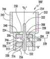
在这方面,图3和图4绘示与外部结构202接合的示例性RF连接器针脚组件200,所述外部结构可为印刷电路板(PCB)。在图3和图4中,RF连接器针脚组件200不被示为具有任何外壳或其他包体以促进论述RF连接器针脚组件200的某些元件。在图3中,RF连接器针脚组件200被绘示为具有单针脚布置,而在图4中,绘示了多针脚布置。RF连接器针脚组件200具有有着第一止动面206的第一电介体204。第一穿通路208(在图3中以虚线示出)从和通过第一止动面206向和通过上面210延伸通过第一电介体204。第二电介体212具有与第一止动面206相对地定位的第二止动面214。第二穿通路216(在图3中以虚线示出)从和通过第二止动面214向和通过下面218延伸通过第二电介体212。第二穿通路216与第一穿通路208对准。第一止动面206和第二止动面214在其间界定间隙220。第一电介体204和第二电介体212可由任何合适的材料所制造,例如PTFE或Torlon(聚酰亚胺酰亚胺(Polyimide-imide))的非限制示例。In this regard, FIGS. 3 and 4 illustrate an example RF
示出了具有第一针脚区段224、第二针脚区段226和第一针脚区段224与第二针脚区段226的接合点230处的环形端箍228的接脚222。第一针脚区段224可移动地安置在第一穿通路208中,而第二针脚区段226可移动地安置在第二穿通路216中,其中环形端箍228定位在间隙220中。如此,接脚222的轴向移动受限于第一止动面206和第二止动面214之间的间隙220中的环形端箍228的移动。此外,第一针脚区段224被调适为提供与外部元件的电气连续性,所述外部元件可为连接器(未示出于图3和图4中)。第二针脚区段226可在远侧上终结于连接特征232中。
特别参照图3,环形端箍228从接脚222径向延伸,使得环形端箍228的外径“AOD”大于第一穿通路208的内径“FID”和第二穿通路216的内径“SID”。环形端箍228的第一侧234接触第一止动面206以将接脚222在第一方向238上的轴向移动限制于第一方向前行限界239。环形端箍228的第二侧236接触第二止动面214以将接脚222在第二方向240上的轴向移动限制于第二方向前行限界241。3, the
连接特征232可被调适为用于连接到外部结构202,所述外部结构如上所述可为PCB 203。如此,连接特征232可被软焊到PCB 203,包括软焊到PCB203的导电轨迹(未示于图3和图4中)。特别参照图4,RF连接器针脚组件200可包括多个接脚222,其中各个接脚222包括第一电介体204和第二电介体212,如上文所论述。在这方面,来自多个接脚222的多个连接特征232可接合PCB 203。如先前所述,PCB 203可能不是完美地扁平或平坦的,反而是可能具有表面不均匀性(例如弓弧,如图4中所绘示)。在连接特征232接合PCB 203时,PCB 203的表面中的不均匀性使得连接特征232轴向移动或“浮动”,且从而使得各别的接脚222轴向移动或“浮动”。其结果是,环形端箍228在第一止动面206和第二止动面214之间的间隙220中移动。这在图4中是通过被定位在各别间隙220的不同部分中的接脚222的环形端箍228来绘示的。因为连接特征232不如上文针对常规浮动针脚组件100所论述地被用作约束器,所以不存在关于接头被强迫抵着载体或头座且危害接脚222到PCB 203的连接行为的问题。接脚222可由任何合适的导电材料所制造,例如镍上的镀黄铜的黄金的非限制性示例。The connection features 232 may be adapted for connection to the
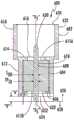
现参照图5-7,绘示了示例性RF连接器针脚组件200’。Rf连接器针脚组件200’与针对图3和图4所论述的RF连接器针脚组件200相同,除了添加了外壳242以外。图5是RF连接器针脚组件200’的分解横截面图,绘示沿着相同的轴“X1”对准的外壳242、第一电介体204、第二电介体212和接脚222。Referring now to Figures 5-7, an exemplary RF connector pin assembly 200' is depicted. The Rf
图6A是已组装的RF连接器针脚组件200’的详细横截面图,其中接脚222在第二方向前行限界241处。图6B是经组装的RF连接器针脚组件200’的详细横截面图,其中接脚222在第一方向前行限界239处。图7是RF连接器针脚组件200’的顶部透视图。FIG. 6A is a detailed cross-sectional view of the assembled RF connector pin assembly 200' with the
继续参照图5、图6A和图6B,外壳242包括第一节段244和第二节段246,其中第二节段246通过间壁248而与第一节段244分离。间壁248具有出入口250,所述出入口延伸于第一节段244和第二节段246之间。第一电介体204定位在第二节段246中。类似地,第二电介体212定位在第二节段246中。第一电介体204和第二电介体212可定位在第二节段246中,使得第一穿通路208、第二穿通路216和出入口250是对准的。第一止动面206和第二止动面214界定第一电介体204和第二电介体212之间的间隙220,其中第一止动面206通过间隙220与第二止动面214分隔距离“A”。With continued reference to FIGS. 5 , 6A and 6B , the
如上文所论述,接脚222包括第一针脚区段224、第二针脚区段226和第一针脚区段224与第二针脚区段226的接合点230处的环形端箍228。可通过以下步骤来组装RF连接器针脚组件200’:将第一电介体204摩擦契合在第二节段246中;将第一针脚区段224安插在第一电介体204的第一穿通路208中;和将第二电介体212摩擦契合在第二节段246中,使得第二针脚区段226安插在第二电介体212的第二穿通路216中。如此,并不需要强迫环形端箍228通过第一穿通路208或第二穿通路216来组装RF连接器针脚组件200’。As discussed above, the
在这方面,第一针脚区段224可移动地安置在第一穿通路208中,而第二针脚区段226可移动地安置在第二穿通路216中,使得接脚222在第一穿通路208和第二穿通路216中在第一方向238和第二方向240上可轴向移动。此外,第一针脚区段224可延伸通过第一穿通路208和通过出入口250进入第一节段244。第一节段244可包括插座252,所述插座具有被调适为接收连接器(例如参照图12)的接收端口254。第一针脚区段224可提供与由插头252的接收端口254所接收的连接器的电气连续性。In this regard, the
第二节段246包括与间壁248相对的开放远端256。如图6B中所示,在接脚222的轴向移动是在第一方向前行限界239上时,连接特征232可在外壳242中。如图6A中所示,在接脚222的轴向移动是在第二方向前行限界241上时,连接特征232可延伸通过外壳242的开放远端256距离“B”。距离“B”可不超过距离“A”,距离“A”是间隙220的尺度。如此,可提供充足的距离以允许接脚222响应于连接特征232通过所述连接特征与外部结构202(举例而言,例如PCB 203(未示出))接合而进行的移动而轴向移动。并且,距离“B”可允许外壳242接触PCB203,使得外壳242可被调适为提供外部元件(例如由插座252的接收端口254所接收的连接器)和PCB 203之间的接地连续性。外壳242可由任何合适的材料所制造,例如镍上的镀黄铜的黄金的非限制性示例。The
图7绘示RF连接器针脚组件200’的看进外壳242的第一节段244的顶部透视图。接脚222、间壁248和出入口250是可见的,插座252和接收端口254也是如此。如下文将更详细论述的,在RF连接器针脚组件200’被安装(也就是连接到PCB 203)时,RF连接器针脚组件200’的顶部可被暴露且是可接取的,以允许连接外部元件(举例而言,例如连接器)。7 illustrates a top perspective view of the RF connector pin assembly 200' looking into the
现参照图8-10,绘示了示例性RF连接器针脚组件300。RF连接器针脚组件300包括与如上文针对图3-7所论述的RF连接器针脚组件200和200’的那些方面类似的某些方面。因此,除了任何实质的差异以外,将不在此文针对RF连接器针脚组件300重复RF连接器针脚组件200和200’的此类类似方面的论述。8-10, an exemplary RF
图8是RF连接器针脚组件300’的分解横截面图,绘示沿着相同的轴“X2”对准的外壳302、第一电介体304、第二电介体306、衬套308和接脚310。图9是已组装的RF连接器针脚组件300的详细横截面图,其中接脚310在第一方向前行限界312处。继续参照图8和图9,外壳302包括第一节段314和第二节段316,其中第二节段316通过间壁318而与第一节段314分离。间壁318中的出入口320延伸于第一节段314和第二节段316之间。第一电介体304、第二电介体306和衬套308定位在第二节段316中,使得第一电介体304中的第一穿通路322、第二电介体306中的第二穿通路324和衬套308中的衬套开口326全是对准的。第二节段316包括与间壁318相对的开放远端348。第一电介体304上的第一止动面328和第二电介体306上的第二止动面330界定间隙332,其中第一止动面328通过间隙332与第二止动面330分隔距离“A”。虽然第一电介体304的侧331在图9中被示为邻接第二电介体306,间隙332仍然形成于由侧331所包围的第一止动面328和第二止动面330之间。第一电介体304和第二电介体306可由任何合适的材料所制造,例如PTFE或Torlon(聚酰亚胺酰亚胺(Polyimide-imide))的非限制示例。8 is an exploded cross-sectional view of RF connector pin assembly 300' showing
接脚310包括第一针脚区段334、第二针脚区段336和第一针脚区段334与第二针脚区段336的接合点340处的环形端箍338。第二针脚区段336可在远侧上终结于连接特征342中。RF连接器针脚组件300可通过以下步骤来组装:将第二电介体306摩擦契合于第二节段316中;将第二针脚区段336安插在第二电介体306的第二穿通路324中;将第一电介体304定位在第二节段316中,使得第一针脚区段334安插在第一电介体304的第一穿通路322中且环形端箍338定位在间隙332中;和将衬套308摩擦契合于第二节段316中在第一电介体304上方,使得第一针脚区段334延伸通过衬套开口326。如此,并不需要强迫环形端箍338通过第一穿通路322、第二穿通路324或衬套开口326来组装RF连接器针脚组件300。接脚308和衬套308可由任何合适的材料所制造,例如镍上的镀黄铜的黄金的非限制性示例。The
在这方面,第一针脚区段334可移动地安置在第一穿通路322中,而第二针脚区段336可移动地安置在第二穿通路324中,使得接脚310可在第一穿通路322和第二穿通路324中在第一方向337和第二方向339上可轴向移动。此外,第一针脚区段334可延伸通过第一穿通路326、衬套开口326和通过出入口320进入第一节段314。第一节段314可包括插座344,所述插座具有被调适为接收连接器(例如参照图12)的接收端口346。第一针脚区段334可提供与由插头344的接收端口346所接收的连接器的电气连续性。In this regard, the
第二节段316包括与间壁318相对的开放远端348。在图9中,接脚310处于第一方向前行限界312处,其中连接特征342定位在外壳302中。用与RF连接器针脚组件200’的方式(如图6A中所示)类似的方式,在接脚310的轴向移动是在第二方向前行限界350处时,连接特征342可延伸通过外壳302的开放远端348距离“B”,所述距离可小于或等于距离“A”(间隙332的尺度)。如此,可提供充足的距离以允许接脚310响应于连接特征342通过所述连接特征与外部结构(举例而言,例如PCB)接合而进行的移动而轴向移动。并且,距离“B”可允许外壳302接触PCB,使得外壳302可被调适为提供外部元件(例如由插座344的接收端口346所接收的连接器)和PCB之间的接地连续性。外壳302可由任何合适的材料所制造,例如镍上的镀黄铜的黄金的非限制性示例。The
图10是RF连接器针脚组件300的看进外壳302的第一节段314的顶部透视图。接脚310、间壁318、衬套308和出入口320是可见的,插座344和接收端口346也是如此。如下文将更详细论述的,RF连接器针脚组件300的顶部可被暴露且是可接取的,以允许连接外部元件(举例而言,例如连接器)。FIG. 10 is a top perspective view of the RF
现参照图11A和图11B,绘示了示例性RF连接器针脚组件400。RF连接器针脚组件400包括与如上文针对图3-7所论述的RF连接器针脚组件200、200’的那些方面类似的某些方面。因此,除了任何实质的差异以外,将不在此文针对RF连接器针脚组件400重复RF连接器针脚组件200、200’的此类类似方面的论述。Referring now to FIGS. 11A and 11B , an exemplary RF
图11A和图11B是已组装的RF连接器针脚组件400的详细横截面图,绘示沿着相同的轴“X3”对准的外壳402、第一电介体404、第二电介体406和直角接脚408(也称为直角连接器针脚)。图11A是已组装的RF连接器针脚组件400的详细横截面图,其中直角接脚408在第二方向前行限界410处。图11B是已组装的RF连接器针脚组件400的详细横截面图,其中直角接脚408在第一方向前行限界412处。11A and 11B are detailed cross-sectional views of the assembled RF
继续参照图11A和图11B,外壳402包括第一节段414和第二节段416,其中第二节段416通过间壁418而与第一节段414分离。间壁418中的出入口420延伸于第一节段414和第二节段416之间。第一电介体404定位在第二节段416中。类似地,第二电介体406定位在第二节段416中。第一电介体404和第二电介体406可定位在第二节段416中,使得第一电介体404中的第一穿通路422、第二穿通路424和出入口420是对准的。第一止动面426和第二止动面428界定第一电介体404和第二电介体406之间的间隙430,其中第一止动面426通过间隙430与第二止动面428分隔距离“A”。第一电介体404和第二电介体406可由任何合适的材料所制造,例如PTFE或Torlon(聚酰亚胺酰亚胺(Polyimide-imide))的非限制示例。With continued reference to FIGS. 11A and 11B , the
直角接脚408包括第一针脚区段432、第二针脚区段434、第一针脚区段432与第二针脚区段434的接合点438处的环形端箍436、和从第二针脚区段434相对于所述第二针脚区段以一定角度延伸的第三针脚区段440。具体而言,第三针脚区段440相对于第二针脚区段434是大约垂直的(也就是呈大约直角)。第三针脚区段440一体地连接到第二针脚区段434。第三针脚区段440可在远侧上终结于连接特征442中。The
RF连接器针脚组件400可通过以下步骤来组装:将第一电介体404摩擦契合在第二节段416中;将第三针脚区段440安插通过第二电介体406的第二穿通路424;将第二针脚区段434安插在第二电介体406的第二穿通路424中;和将第二电介体406摩擦契合在第二节段416中,使得第一针脚区段432安插在第一电介体404的第一穿通路422中。如此,并不需要强迫环形端箍436通过第一穿通路422或第二穿通路424来组装RF连接器针脚组件400。直角接脚408可由任何合适的材料所制造,例如镍上的镀黄铜的黄金的非限制性示例。The RF
在这方面,第一针脚区段432可移动地安置在第一穿通路422中,而第二针脚区段434可移动地安置在第二穿通路424中,使得直角接脚408可在第一穿通路422和第二穿通路424中在第一方向444和第二方向446上可轴向移动。此外,第一针脚区段432可延伸通过第一穿通路422和通过出入口420进入第一节段414。第一节段414可包括插座448,所述插座具有被调适为接收连接器(例如参照图12)的接收端口450。第一针脚区段432可提供与由插头448的接收端口450所接收的连接器的电气连续性。In this regard, the
第二节段416包括与间壁418相对的开放远端452。进一步地,第二节段416包括从开放远端452向上延伸的一或更多个侧壁通道454。具体而言,第三针脚区段440被定位通过所述一或更多个侧壁通道454中的至少一个,其中连接特征442延伸经过第二节段416到外壳402的外部。如图11B中所示,在直角接脚408的轴向移动是在第一方向前行限界412处时,连接特征442在外壳402的外部,第三针脚区段440的至少一部分定位在所述一或更多个侧壁通道454内,且第三针脚区段440的远端456的至少一部分可在外壳402中。如图11A中所示,在直角接脚408的轴向移动是在第二方向前行限界410处时,连接特征442仍然在外壳402的外部,第三针脚区段440至少部分地定位在所述一或更多个侧壁通道454内,且第三针脚区域440的远端456的至少一部分延伸通过外壳402的开放远端452距离“B”。距离“B”可小于或等于距离“A”,距离“A”是间隙430的尺度。如此,可提供充足的距离以允许直角接脚408响应于第三针脚区段440(和连接特征442)通过所述第三针脚区段(和所述连接特征)与外部结构(举例而言,例如PCB 203(参照图4))接合而进行的移动而轴向移动。并且,距离“B”可允许外壳402接触PCB 203,使得外壳402可被调适为提供外部元件(例如由插座448的接收端口450所接收的连接器)和PCB 203之间的接地连续性。外壳402可由任何合适的材料所制造,例如镍上的镀黄铜的黄金的非限制性示例。The
图12是RF连接器针脚组件300的横截面图,所述RF连接器针脚组件连接到PCB 203且其中连接器560安插在接收端口346中。RF连接器针脚组件300与连接器560沿着相同的轴“X4”对准。外壳302的第二节段316接触PCB203,且从而通过外壳302的第一节段314与连接器560的主体562建立接地连续性。接脚310的连接特征342被示为连接到PCB 203的导体,此举可通过将连接特征342软焊到PCB 203上的导电轨迹(未示于图12中)来完成。环形端箍338被示为定位在间隙332的第一方向前行限界312处。第一针脚区段334被示为安插在连接器560中且提供与连接器560的内导体564的连续性以建立从PCB 203通过接脚310到内导体564的连续性。FIG. 12 is a cross-sectional view of RF
现参照图13-14B,绘示了示例性RF连接器针脚组件600。RF连接器针脚组件600包括与图3-12的RF连接器针脚组件200、200’、300、400的那些方面类似的某些方面。因此,除了任何实质的差异以外,将不在此文针对RF连接器针脚组件600重复RF连接器针脚组件200、200’、300、400的此类类似方面的论述。13-14B, an exemplary RF
图13是RF连接器针脚组件600’的分解横截面图,绘示沿着相同的轴“X5”(也示于图14A-14B中)对准的外壳602、电介体604、衬套606和接脚608。Figure 13 is an exploded cross-sectional view of RF connector pin assembly 600' showing
图14A是已组装的RF连接器针脚组件600的详细横截面图,其中接脚608在第一位置处。图6B是已组装的RF连接器针脚组件600的详细横截面图,其中接脚608在第二位置处。14A is a detailed cross-sectional view of the assembled RF
继续参照图13-14B,外壳602包括第一节段610和第二节段612,其中第二节段612通过间壁614而与第一节段610分离。间壁614中的出入口616延伸于第一节段610和第二节段612之间。电介体604和衬套606定位在第二节段612中,使得电介体604中的穿通路618和衬套606中的衬套开口620全是对准的。穿通路618包括内径TPID且延伸于电介体604的第一面615A和第二面615B之间。第二节段612包括与间壁614相对的开放远端622。电介体604可由任何合适的材料所制造,例如PTFE或Torlon(聚酰亚胺酰亚胺(Polyimide-imide))的非限制示例。With continued reference to FIGS. 13-14B , the
接脚608(也称为轴杆)可在远侧上终结于连接特征624中。接脚608包括轴杆外径SOD。RF连接器针脚组件600可通过以下步骤来组装:将电介体604与衬套606摩擦契合(例如电介体604的外表面摩擦接合衬套606的内表面);将衬套606摩擦契合在第二节段612中(例如衬套606的外表面摩擦接合第二节段612的内表面),使得电介体604安插在第二节段612中;和将接脚608摩擦契合在电介体604的穿通路618中,使得接脚608的至少一部分(和连接特征624)延伸经过开放远端622。如此,并不需要强迫接脚608通过穿通路618来组装RF连接器针脚组件600。接脚608和衬套606可由任何合适的材料所制造,例如镍上的镀黄铜的黄金的非限制性示例。Pins 608 (also referred to as shafts) may terminate distally in connection features 624 .
在这方面,在经组装时,衬套606将电介体604和接脚608安装在外壳602内,且也在电介体604的外表面和外壳602的第二节段612的内表面之间提供距离“A”。距离“A”减少在将电介体604和接脚608组装在外壳602的第二节段612内的期间的接脚608上的应力。此外,电介体604可能在RF连接器针脚组件600被安装到PCB时由于热而膨胀。距离“A”允许电介体604的径向膨胀,而进一步减少接脚608上的应力。进一步地,距离“A”防止电介体604的轴向膨胀,此举对于维持可靠度和电性能特性来说是重要的,因为RF连接器针脚组件600的电气特征可取决于电介体604和外壳602的开放远端622之间的距离。In this regard, when assembled, bushing 606 mounts
接脚608可移动地安置在穿通路618中,使得接脚608可在穿通路618中在第一方向626和第二方向628上可轴向移动。此外,接脚608的近端630可延伸经过穿通路618和通过出入口616进入第一节段610。第一节段610可包括插座632,所述插座具有被调适为接收连接器(例如参照图12)的接收端口634。接脚608可提供与由插头632的接收端口634所接收的连接器的电气连续性。The
在图14A中,接脚608在第一位置处,其中连接特征624延伸通过外壳602的开放远端622距离“B”。如此,可提供充足的距离以允许接脚608响应于连接特征624通过所述连接特征与外部结构(举例而言,例如PCB)接合而进行的移动而轴向移动。并且,距离“B”可允许外壳602接触PCB,使得外壳602可被调适为提供外部元件(例如由插座632的接收端口634所接收的连接器)和PCB之间的接地连续性。外壳602可由任何合适的材料所制造,例如镍上的镀黄铜的黄金的非限制性示例。In FIG. 14A, the
接脚608与电介体604的摩擦接合足以使得接脚608在RF连接器针脚组件600接合或脱离连接器时不在第一方向626上移动(例如参照图12)。然而,可有目的地或有意地克服此摩擦接合以变更接脚608相对于电介体604和外壳602的位置。如此,接脚608的连接特征624相对于外壳602的开放远端622的距离允许有意的移动,但防止意外的移动。The frictional engagement of the
现参照图15A和15B,绘示了示例性RF连接器针脚组件700。RF连接器针脚组件700包括与图3-14B的RF连接器针脚组件200、200’、300、400、600的那些方面类似的某些方面。因此,除了任何实质的差异以外,将不在此文针对RF连接器针脚组件700重复RF连接器针脚组件200、200’、300、400、600的此类类似方面的论述。Referring now to Figures 15A and 15B, an exemplary RF
图15A是已组装的RF连接器针脚组件700’的详细横截面图,绘示沿着相同的轴“X6”对准的外壳702、电介体704、衬套706和接脚708,且其中接脚708在第一位置处。图15B是已组装的RF连接器针脚组件700的详细横截面图,其中接脚708在第二位置处。15A is a detailed cross-sectional view of an assembled RF connector pin assembly 700' showing
继续参照图15A-15B,外壳702包括第一节段710和第二节段712,其中第二节段712通过间壁714而与第一节段710分离。间壁714中的出入口716延伸于第一节段710和第二节段712之间。电介体704和衬套706定位在第二节段712中,使得电介体704中的穿通路718和衬套706中的衬套开口720全是对准的。穿通路718包括内径TPID且延伸于电介体704的第一面715A和第二面715B之间。第二节段712包括与间壁714相对的开放远端722。电介体704可由任何合适的材料所制造,例如PTFE或Torlon(聚酰亚胺酰亚胺(Polyimide-imide))的非限制示例。With continued reference to FIGS. 15A-15B , the
接脚708包括第一针脚区段709A(也称为轴杆)和第二针脚区段709B(也称为轴杆)。第一针脚区段709A和第二针脚区段709B中的每一个包括轴杆外径SOD。第二针脚区段709B从第一针脚区段709A相对于所述第一针脚区段以一定角度延伸。具体而言,第二针脚区段709B相对于第一针脚区段709A是大约垂直的(也就是呈大约直角)。第二针脚区段709B一体地连接到第一针脚区段709A。第二针脚区段709B可在远侧上终结于连接特征724中。
RF连接器针脚组件700可通过以下步骤来组装:将电介体704与衬套706摩擦契合(例如电介体704的外表面摩擦接合衬套706的内表面);将衬套706摩擦契合在第二节段712中(例如衬套706的外表面摩擦接合第二节段712的内表面),使得电介体704安插在第二节段712中;和将接脚708的第一针脚区段709A摩擦契合在电介体704的穿通路718中,使得接脚708的第一针脚区段709A的至少一部分(和连接特征724)延伸经过开放远端722。如此,并不需要强迫接脚708通过穿通路718来组装RF连接器针脚组件700。接脚708和衬套706可由任何合适的材料所制造,例如镍上的镀黄铜的黄金的非限制性示例。The RF
在这方面,在组装时,衬套706将电介体704和接脚708安装在外壳702内,且也在电介体704的外表面和外壳702的第二节段712的内表面之间提供距离“A”。距离“A”减少在将电介体704和接脚708组装在外壳702的第二节段712内的期间的接脚708上的应力。此外,电介体704可能在RF连接器针脚组件700被安装到PCB时由于热而膨胀。距离“A”允许电介体704的径向膨胀,而进一步减少接脚708的第一针脚区段709A上的应力。进一步地,距离“A”防止电介体704的轴向膨胀,此举对于维持可靠度和电性能特性来说是重要的,因为RF连接器针脚组件700的电气特征可取决于电介体704和外壳702的开放远端722之间的距离。In this regard, when assembled, bushing 706 mounts
接脚708的第一针脚区段709A可移动地安置在穿通路718中,使得接脚708的第一针脚区段709A可在穿通路718中在第一方向726和第二方向728上可轴向移动。此外,接脚708的第一针脚区段709A的近端730可延伸经过穿通路718和通过出入口716进入第一节段710。第一节段710可包括插座732,所述插座具有被调适为接收连接器(例如参照图12)的接收端口734。接脚708的第一针脚区段709A可提供与由插头732的接收端口734所接收的连接器的电气连续性。The
第二节段712包括与间壁714相对的开放远端722。进一步地,第二节段712包括从开放远端722向上延伸的一或更多个侧壁通道721。具体而言,第二针脚区段709B被定位通过所述一或更多个侧壁通道721中的至少一个,其中连接特征724延伸经过第二节段712到外壳702的外部。The
在图15A中,接脚708在第一位置处,其中第二针脚区段709B的远端723延伸通过外壳702的开放远端722距离“B”,且连接特征724在外壳702外部。如图15B中所示,在接脚708的轴向移动是在第一方向726上移动时,连接特征724仍然在外壳702外部,且第二针脚区段709B至少部分地定位在所述一或更多个侧壁通道721内。如此,可提供充足的距离以允许接脚708响应于连接特征724通过所述连接特征与外部结构(举例而言,例如PCB)接合而进行的移动而轴向移动。并且,距离“B”可允许外壳702接触PCB,使得外壳702可被调适为提供外部元件(例如由插座732的接收端口734所接收的连接器)和PCB之间的接地连续性。外壳702可由任何合适的材料所制造,例如镍上的镀黄铜的黄金的非限制性示例。In FIG. 15A , the
接脚708与电介体704的摩擦接合足以使得接脚708在RF连接器针脚组件700接合或脱离连接器时不在第一方向726上移动(例如参照图12)。然而,可有目的地或有意地克服此摩擦接合以变更接脚708相对于电介体704和外壳702的位置。如此,接脚708的连接特征724相对于外壳702的开放远端722的距离允许有意的移动,但防止意外的移动。The frictional engagement of the
图16是RF连接器针脚组件600的横截面图,所述RF连接器针脚组件连接到PCB 203且其中连接器560安插在接收端口634中。RF连接器针脚组件600与连接器560沿着相同的轴“X7”对准。外壳602的第二节段612接触PCB203,且从而通过外壳602的第一节段610与连接器560的主体562建立接地连续性。接脚608的连接特征624被示为连接到PCB 203的导体,此举可通过将连接特征624软焊到PCB 203上的导电轨迹(未示于图16中)来完成。接脚608的近端630安插在连接器560中且提供与连接器560的内导体564的连续性以建立从PCB 203通过接脚608到内导体564的连续性。16 is a cross-sectional view of RF
图17-22是多针脚RF连接器插头块组件800的视图。RF连接器插头块组件800包括可移除地安装在连接器插头块802中的多个RF连接器针脚组件300(参照图8和图9)。图17是多针脚RF连接器插头块800的顶视图,所述多针脚RF连接器插头块组件在其中安置有多个RF连接器针脚组件300。图18是连接器插头块802的横截面图,其中连接器针脚组件300安置在所述连接器插头块中。图19是不具有RF连接器针脚组件300的连接器插头块802的顶视图。图20是不具有RF连接器针脚组件300的连接器插头块802的横截面图。图21是连接到PCB203的多针脚RF连接器插头块800的顶视图。图22是连接到PCB 203的多针脚RF连接器插头块800的侧视图。17-22 are views of a multi-pin RF connector
通过将多个外壳302可移除地安装在多个外壳端口804中的各别外壳端口中来将RF连接器针脚组件300中的每一个可移除地安装在连接器插头块802中。应注意,虽然图17-22绘示RF连接器针脚组件300,但也可将RF连接器针脚组件200、200’、400、600、700可移除地安装在连接器插头块802中,且图17-22的论述也适用于RF连接器针脚组件200、200’、400、600、700。如图21和图22中可见的,连接器插头块802安装到外部结构202(例如PCB203)。外壳302可移除地安装在外壳端口804中,使得外壳302的第二节段316接触PCB203,且从而通过外壳302的第一节段314与连接器560的主体562(例如参照图12)建立接地连续性。如此,相对于外壳302中的另一个而可独立移除地安装了外壳302中的一个。此外,外壳302中的一个中的接脚310相对于外壳302中的另一个中的接脚310在第一方向337和第二方向339(参照图9)上可独立轴向移动。各个接脚310的连接特征342(示于图22中)连接到PCB 203的导电轨迹806(示于图21中),此举可通过将连接特征342软焊到导电轨迹806来完成。并且,外壳302的第二节段316(示于图22)中的每一个接触PCB 203且从而建立外壳302和PCB 203之间的接地连续性。如此,RF连接器针脚组件300可包括使用连接器插头块802来连接到PCB 203的多个外壳302和多个接脚310。连接器插头块802可由任何合适的塑料材料所制造,且可使用任何合适的固定器808来安装到外部结构202。Each of the RF
图23描绘一种用于组装RF连接器针脚组件200、200’、300、400的方法,所述方法包括以下步骤:提供外壳242、302、402,所述外壳包括第一节段244、314、414、第二节段246、316、416和间壁248、318、418,所述间壁将第一节段244、314、414与第二节段246、316、416分离(方块900);将第一电介体204、304、404安插在外壳242、302、402的第二节段246、316、416中,第一电介体204、304、404包括第一穿通路208、322、422和第一止动面206、328、426(方块902);将第二电介体212、306、406安插在外壳242、302、402的第二节段246、316、416中,第二电介体212、306、406包括第二穿通路216、324、424和第二止动面214、330、428,其中第二穿通路216、324、242与第一穿通路208、322、422对准,且其中第一止动面206、328、426和第二止动面214、330、428形成间隙220、332、430(方块904);将接脚222、310、408可移动地定位在外壳242、302、402中,接脚222、310、408包括第一针脚区段224、334、432、第二针脚区段226、336、434和第一针脚区段224、334、432与第二针脚区段226、336、434的接合点230、340、438处的环形端箍228、338、436,其中第一针脚区段224、334、432可移动地安置在第一穿通路208、322、422中,且第二针脚区段226、336、434可移动地安置在第二穿通路216、324、424中,且其中接脚222、310、408在第一穿通路208、322、422和第二穿通路216、324、424中在第一方向238、337、444和第二方向240、339、446上可轴向移动,且其中环形端箍228、338、436定位在间隙220、332、430中而不越过第一穿通路208、322、422和第二穿通路216、324、424(方块906)。23 depicts a method for assembling an RF connector pin assembly 200, 200', 300, 400, the method comprising the steps of: providing a housing 242, 302, 402 including a first segment 244, 314 ; The first dielectric body 204, 304, 404 is inserted in the second segment 246, 316, 416 of the housing 242, 302, 402, the first dielectric body 204, 304, 404 includes the first through-passages 208, 322, 422 and the first stop surfaces 206, 328, 426 (block 902); the second dielectric body 212, 306, 406 is inserted into the second segment 246, 316, 416 of the housing 242, 302, 402, the second electrical The mediators 212 , 306 , 406 include second through passages 216 , 324 , 424 and second stop surfaces 214 , 330 , 428 , wherein the second through passages 216 , 324 , 242 are opposite to the first through passages 208 , 322 , 422 alignment and wherein first stop surfaces 206, 328, 426 and second stop surfaces 214, 330, 428 form gaps 220, 332, 430 (block 904); pins 222, 310, 408 are removably positioned at In the housings 242, 302, 402, the pins 222, 310, 408 include the first pin sections 224, 334, 432, the second pin sections 226, 336, 434, the first pin sections 224, 334, 432 and the The annular end band 228, 338, 436 at the junction 230, 340, 438 of the two stitch sections 226, 336, 434, wherein the first stitch section 224, 334, 432 is movably disposed in the first through passage 208, 322, 422, and the second pin segments 226, 336, 434 are movably disposed in the second through-passages 216, 324, 424, and wherein the pins 222, 310, 408 are in the first through-passages 208, 322, 422 and second through passages 216 , 324 , 424 are axially movable in first directions 238 , 337 , 444 and second directions 240 , 339 , 446 and wherein annular end collars 228 , 338 , 436 are positioned in gap 220 , 332, 430 without crossing the first through passages 208, 322, 422 and the second through passages 216, 324, 424 (block 906).
除非另有明确表明,绝不要本文中所阐述的任何方法被解读为需要其步骤以特定的顺序执行。据此,若方法请求项实际上并不记载要由其步骤所遵循的顺序或在请求项或说明书中并未另有具体表明将步骤限于特定顺序,则绝不欲推断任何特定顺序。Unless explicitly stated otherwise, any method set forth herein should in no way be construed as requiring that its steps be performed in a particular order. Accordingly, no particular order is intended to be inferred if a method claim does not actually recite the order to be followed by its steps or does not specifically state otherwise in the claim or in the specification to limit the steps to a particular order.
本领域中的技术人员将理解到,在不脱离本发明的精神或范围的情况下,可作出各种更改和变化。因为本领域中的技术人员可以想到并入本发明的精神和本质的所公开的实施方式的更改组合、子组合和变化,所以本发明应被解读为包括随附权利要求书和其等效物的范围内的一切事物。It will be understood by those skilled in the art that various modifications and changes can be made without departing from the spirit or scope of the invention. Since modified combinations, sub-combinations and variations of the disclosed embodiments that incorporate the spirit and essence of the inventions may occur to those skilled in the art, the inventions should be construed to include the appended claims and their equivalents everything within the range.
Claims (24)
Applications Claiming Priority (3)
| Application Number | Priority Date | Filing Date | Title |
|---|---|---|---|
| US15/581,913 | 2017-04-28 | ||
| US15/581,913US10199753B2 (en) | 2017-04-28 | 2017-04-28 | Multi-pin connector block assembly |
| PCT/US2018/027985WO2018200262A1 (en) | 2017-04-28 | 2018-04-17 | Multi-pin connector block assembly |
Publications (2)
| Publication Number | Publication Date |
|---|---|
| CN110710058Atrue CN110710058A (en) | 2020-01-17 |
| CN110710058B CN110710058B (en) | 2022-05-10 |
Family
ID=62116612
Family Applications (1)
| Application Number | Title | Priority Date | Filing Date |
|---|---|---|---|
| CN201880037237.3AActiveCN110710058B (en) | 2017-04-28 | 2018-04-17 | Multipin Connector Plug Block Assembly |
Country Status (5)
| Country | Link |
|---|---|
| US (2) | US10199753B2 (en) |
| EP (1) | EP3616268B1 (en) |
| CN (1) | CN110710058B (en) |
| TW (1) | TWI761494B (en) |
| WO (1) | WO2018200262A1 (en) |
Cited By (3)
| Publication number | Priority date | Publication date | Assignee | Title |
|---|---|---|---|---|
| CN113437038A (en)* | 2020-03-23 | 2021-09-24 | 珠海格力电器股份有限公司 | Pin, power device, manufacturing method of power device and packaging mold |
| WO2021189877A1 (en)* | 2020-03-23 | 2021-09-30 | 珠海格力电器股份有限公司 | Pin, power device, method for manufacturing power device, and packaging mould |
| CN114665345A (en)* | 2022-03-30 | 2022-06-24 | 中国电子科技集团公司第十研究所 | Coupling type radio frequency connector |
Families Citing this family (4)
| Publication number | Priority date | Publication date | Assignee | Title |
|---|---|---|---|---|
| CN110277706A (en)* | 2019-07-09 | 2019-09-24 | 东莞市联晨鑫电子科技有限公司 | RF connector |
| US11539167B2 (en) | 2020-09-17 | 2022-12-27 | Carlisle Interconnect Technologies, Inc. | Adjustable push on connector/adaptor |
| US11502440B2 (en) | 2020-10-23 | 2022-11-15 | Carlisle Interconnect Technologies, Inc. | Multiport connector interface system |
| US20230163537A1 (en)* | 2021-11-22 | 2023-05-25 | Corning Optical Communications Rf Llc | Devices, assemblies, and methods for terminating coaxial radiofrequency ports |
Citations (3)
| Publication number | Priority date | Publication date | Assignee | Title |
|---|---|---|---|---|
| EP0449570A1 (en)* | 1990-03-28 | 1991-10-02 | Molex Incorporated | Multi-pin electrical connector with terminal pins |
| US5769652A (en)* | 1996-12-31 | 1998-06-23 | Applied Engineering Products, Inc. | Float mount coaxial connector |
| EP2211228A2 (en)* | 2009-01-23 | 2010-07-28 | Samsung Electronics Co., Ltd. | Backlight assembly and display device having the same |
Family Cites Families (36)
| Publication number | Priority date | Publication date | Assignee | Title |
|---|---|---|---|---|
| US3764959A (en) | 1972-07-18 | 1973-10-09 | Astrolab | Universal coaxial cable connector |
| US4187481A (en) | 1977-12-23 | 1980-02-05 | Bunker Ramo Corporation | EMI Filter connector having RF suppression characteristics |
| US4657323A (en) | 1986-01-27 | 1987-04-14 | Itt Corporation | D-subminature filter connector |
| JPH0338769Y2 (en)* | 1989-08-01 | 1991-08-15 | ||
| JP2563708Y2 (en)* | 1990-11-30 | 1998-02-25 | 矢崎総業株式会社 | connector |
| US5169347A (en) | 1991-10-15 | 1992-12-08 | Molex Incorporated | Slip-off electrical connector header |
| US5213533A (en)* | 1992-04-23 | 1993-05-25 | Intercon Systems, Inc. | Electrical connector block assembly |
| JP2527144Y2 (en)* | 1992-11-19 | 1997-02-26 | モレックス インコーポレーテッド | Electrical connector for connecting printed circuit boards |
| US5242311A (en)* | 1993-02-16 | 1993-09-07 | Molex Incorporated | Electrical connector header with slip-off positioning cover and method of using same |
| US5683255A (en) | 1993-12-03 | 1997-11-04 | Menze; Marion John | Radio frequency connector assembly |
| US5850693A (en)* | 1995-01-31 | 1998-12-22 | Berg Technology, Inc. | Method of manufacturing an array of surface mount contacts |
| US5563562A (en) | 1995-03-24 | 1996-10-08 | Itt Industries, Inc. | RF feed-through connector |
| JP3056993B2 (en)* | 1995-12-28 | 2000-06-26 | 株式会社ハーネス総合技術研究所 | Connection structure of electrical junction box for instrument panel harness |
| DE19653676C1 (en) | 1996-12-16 | 1998-01-29 | Siemens Ag | Connection between medium voltage switch zones |
| US6431880B1 (en)* | 1998-06-22 | 2002-08-13 | Cooper Technologies | Modular terminal fuse block |
| ATE244943T1 (en) | 1999-03-02 | 2003-07-15 | Huber+Suhner Ag | PCB COAXIAL CONNECTION |
| US6716065B1 (en)* | 2000-06-01 | 2004-04-06 | Leftek International, Llc | Electrical systems with paired bus connectors |
| US6659786B2 (en) | 2001-04-25 | 2003-12-09 | Tyco Electronics Amp Gmbh | Electrical connector |
| CA2453637C (en) | 2003-12-18 | 2009-04-07 | Weco Electrical Connectors Inc. | Self-locking terminal pin |
| GB2417618B (en) | 2004-08-31 | 2009-03-04 | Itt Mfg Enterprises Inc | Coaxial connector |
| US7037131B1 (en)* | 2004-12-17 | 2006-05-02 | Liang Tai Co., Ltd. | Adjustable locking device |
| US7083462B1 (en)* | 2005-11-03 | 2006-08-01 | Liang Tei Co., Ltd. | Adjustable buckling structure for connectors |
| MY147876A (en)* | 2005-12-05 | 2013-01-31 | Nhk Spring Co Ltd | Probe card |
| US7607929B1 (en) | 2008-06-30 | 2009-10-27 | Tyco Electronics Corporation | Electrical connector assembly having spring loaded electrical connector |
| US7857669B1 (en) | 2009-08-05 | 2010-12-28 | Hamilton Sundstrand Corporation | High power electrical interface connection |
| US20120077356A1 (en)* | 2010-09-29 | 2012-03-29 | Omron Corporation | Socket for electrolytic capacitors |
| US9444197B2 (en) | 2012-03-19 | 2016-09-13 | Holland Electronics, Llc | Shielded and multishielded coaxial connectors |
| US9112323B2 (en) | 2012-03-19 | 2015-08-18 | Holland Electronics, Llc | Shielded and multishielded coaxial connectors |
| EP2896094B1 (en)* | 2012-09-12 | 2020-04-08 | Smiths Interconnect Americas, Inc. | Electrical connector |
| US9356374B2 (en) | 2013-01-09 | 2016-05-31 | Amphenol Corporation | Float adapter for electrical connector |
| US9735521B2 (en) | 2013-01-09 | 2017-08-15 | Amphenol Corporation | Float adapter for electrical connector |
| JP5606588B1 (en)* | 2013-05-20 | 2014-10-15 | イリソ電子工業株式会社 | connector |
| US9362633B2 (en) | 2013-11-07 | 2016-06-07 | Pds Electronics, Inc. | Hybridized coaxial cable connector |
| US9281619B2 (en)* | 2014-04-11 | 2016-03-08 | Delphi Technologies, Inc. | Vibration resistant connector system with connector position assurance device |
| TWM517455U (en)* | 2015-11-06 | 2016-02-11 | Amphenol East Asia Electronic Technology Shenzhen Co Ltd | Board to board connector |
| JP6422905B2 (en)* | 2016-03-09 | 2018-11-14 | 矢崎総業株式会社 | connector |
- 2017
- 2017-04-28USUS15/581,913patent/US10199753B2/enactiveActive
- 2018
- 2018-04-17WOPCT/US2018/027985patent/WO2018200262A1/ennot_activeCeased
- 2018-04-17CNCN201880037237.3Apatent/CN110710058B/enactiveActive
- 2018-04-17EPEP18722847.3Apatent/EP3616268B1/enactiveActive
- 2018-04-19TWTW107113309Apatent/TWI761494B/enactive
- 2018-12-19USUS16/226,155patent/US10707595B2/enactiveActive
Patent Citations (3)
| Publication number | Priority date | Publication date | Assignee | Title |
|---|---|---|---|---|
| EP0449570A1 (en)* | 1990-03-28 | 1991-10-02 | Molex Incorporated | Multi-pin electrical connector with terminal pins |
| US5769652A (en)* | 1996-12-31 | 1998-06-23 | Applied Engineering Products, Inc. | Float mount coaxial connector |
| EP2211228A2 (en)* | 2009-01-23 | 2010-07-28 | Samsung Electronics Co., Ltd. | Backlight assembly and display device having the same |
Cited By (4)
| Publication number | Priority date | Publication date | Assignee | Title |
|---|---|---|---|---|
| CN113437038A (en)* | 2020-03-23 | 2021-09-24 | 珠海格力电器股份有限公司 | Pin, power device, manufacturing method of power device and packaging mold |
| WO2021189877A1 (en)* | 2020-03-23 | 2021-09-30 | 珠海格力电器股份有限公司 | Pin, power device, method for manufacturing power device, and packaging mould |
| CN114665345A (en)* | 2022-03-30 | 2022-06-24 | 中国电子科技集团公司第十研究所 | Coupling type radio frequency connector |
| CN114665345B (en)* | 2022-03-30 | 2023-11-07 | 中国电子科技集团公司第十研究所 | Coupling type radio frequency connector |
Also Published As
| Publication number | Publication date |
|---|---|
| US10199753B2 (en) | 2019-02-05 |
| US20180316103A1 (en) | 2018-11-01 |
| TW201842715A (en) | 2018-12-01 |
| US10707595B2 (en) | 2020-07-07 |
| EP3616268B1 (en) | 2025-05-28 |
| TWI761494B (en) | 2022-04-21 |
| US20190148851A1 (en) | 2019-05-16 |
| EP3616268A1 (en) | 2020-03-04 |
| WO2018200262A1 (en) | 2018-11-01 |
| CN110710058B (en) | 2022-05-10 |
Similar Documents
| Publication | Publication Date | Title |
|---|---|---|
| CN110710058B (en) | Multipin Connector Plug Block Assembly | |
| US11056807B2 (en) | Float connector for interconnecting printed circuit boards | |
| JP6987231B2 (en) | Coaxial connector | |
| US4957456A (en) | Self-aligning RF push-on connector | |
| TWI540795B (en) | Electrical connector assembly having direct connection terminals | |
| US11355880B2 (en) | Coaxial connector with axially-floating inner contact | |
| JP2008529255A (en) | New coaxial connector | |
| TWM647732U (en) | Receptacle connector and metal housing for the same | |
| JP2007525808A (en) | Connector device | |
| JP2007503591A (en) | Coaxial probe interface | |
| US11728599B2 (en) | Coaxial connectors for board-to-board interconnection | |
| KR102735547B1 (en) | Integral RF connector having grounding contact tabs arranged in a crown shape and grouped connectors comprising a plurality of such integral connectors | |
| WO1998016971A9 (en) | Subminiature matched impedance rf coaxial connector | |
| CN110622362B (en) | Radio Frequency (RF) connector pin assembly | |
| CN210866559U (en) | Coaxial Connectors and Board-to-Board Connector Assemblies | |
| CN105789945A (en) | Float adapter for electrical connector | |
| CN113727521B (en) | Circuit board with plug connector interface and electrical plug connector device with such circuit board | |
| TW201347319A (en) | Coaxial connector | |
| US20070146103A1 (en) | Resistor board and attenuator having the same | |
| KR20040052807A (en) | A coaxial connector | |
| HK1244357A1 (en) | Float adapter for electrical connector and method for making the same |
Legal Events
| Date | Code | Title | Description |
|---|---|---|---|
| PB01 | Publication | ||
| PB01 | Publication | ||
| SE01 | Entry into force of request for substantive examination | ||
| SE01 | Entry into force of request for substantive examination | ||
| GR01 | Patent grant | ||
| GR01 | Patent grant |