CN110709999A - TFT substrate and scanning antenna with TFT substrate - Google Patents
TFT substrate and scanning antenna with TFT substrateDownload PDFInfo
- Publication number
- CN110709999A CN110709999ACN201880036309.2ACN201880036309ACN110709999ACN 110709999 ACN110709999 ACN 110709999ACN 201880036309 ACN201880036309 ACN 201880036309ACN 110709999 ACN110709999 ACN 110709999A
- Authority
- CN
- China
- Prior art keywords
- electrode
- layer
- conductive
- gate
- source
- Prior art date
- Legal status (The legal status is an assumption and is not a legal conclusion. Google has not performed a legal analysis and makes no representation as to the accuracy of the status listed.)
- Pending
Links
Images


Classifications
- H—ELECTRICITY
- H10—SEMICONDUCTOR DEVICES; ELECTRIC SOLID-STATE DEVICES NOT OTHERWISE PROVIDED FOR
- H10D—INORGANIC ELECTRIC SEMICONDUCTOR DEVICES
- H10D86/00—Integrated devices formed in or on insulating or conducting substrates, e.g. formed in silicon-on-insulator [SOI] substrates or on stainless steel or glass substrates
- H10D86/40—Integrated devices formed in or on insulating or conducting substrates, e.g. formed in silicon-on-insulator [SOI] substrates or on stainless steel or glass substrates characterised by multiple TFTs
- H10D86/481—Integrated devices formed in or on insulating or conducting substrates, e.g. formed in silicon-on-insulator [SOI] substrates or on stainless steel or glass substrates characterised by multiple TFTs integrated with passive devices, e.g. auxiliary capacitors
- H—ELECTRICITY
- H10—SEMICONDUCTOR DEVICES; ELECTRIC SOLID-STATE DEVICES NOT OTHERWISE PROVIDED FOR
- H10D—INORGANIC ELECTRIC SEMICONDUCTOR DEVICES
- H10D30/00—Field-effect transistors [FET]
- H10D30/60—Insulated-gate field-effect transistors [IGFET]
- H10D30/67—Thin-film transistors [TFT]
- H10D30/674—Thin-film transistors [TFT] characterised by the active materials
- H10D30/6741—Group IV materials, e.g. germanium or silicon carbide
- H10D30/6743—Silicon
- G—PHYSICS
- G02—OPTICS
- G02F—OPTICAL DEVICES OR ARRANGEMENTS FOR THE CONTROL OF LIGHT BY MODIFICATION OF THE OPTICAL PROPERTIES OF THE MEDIA OF THE ELEMENTS INVOLVED THEREIN; NON-LINEAR OPTICS; FREQUENCY-CHANGING OF LIGHT; OPTICAL LOGIC ELEMENTS; OPTICAL ANALOGUE/DIGITAL CONVERTERS
- G02F1/00—Devices or arrangements for the control of the intensity, colour, phase, polarisation or direction of light arriving from an independent light source, e.g. switching, gating or modulating; Non-linear optics
- G02F1/01—Devices or arrangements for the control of the intensity, colour, phase, polarisation or direction of light arriving from an independent light source, e.g. switching, gating or modulating; Non-linear optics for the control of the intensity, phase, polarisation or colour
- G02F1/13—Devices or arrangements for the control of the intensity, colour, phase, polarisation or direction of light arriving from an independent light source, e.g. switching, gating or modulating; Non-linear optics for the control of the intensity, phase, polarisation or colour based on liquid crystals, e.g. single liquid crystal display cells
- G02F1/133—Constructional arrangements; Operation of liquid crystal cells; Circuit arrangements
- G02F1/1333—Constructional arrangements; Manufacturing methods
- G02F1/1345—Conductors connecting electrodes to cell terminals
- G—PHYSICS
- G02—OPTICS
- G02F—OPTICAL DEVICES OR ARRANGEMENTS FOR THE CONTROL OF LIGHT BY MODIFICATION OF THE OPTICAL PROPERTIES OF THE MEDIA OF THE ELEMENTS INVOLVED THEREIN; NON-LINEAR OPTICS; FREQUENCY-CHANGING OF LIGHT; OPTICAL LOGIC ELEMENTS; OPTICAL ANALOGUE/DIGITAL CONVERTERS
- G02F1/00—Devices or arrangements for the control of the intensity, colour, phase, polarisation or direction of light arriving from an independent light source, e.g. switching, gating or modulating; Non-linear optics
- G02F1/01—Devices or arrangements for the control of the intensity, colour, phase, polarisation or direction of light arriving from an independent light source, e.g. switching, gating or modulating; Non-linear optics for the control of the intensity, phase, polarisation or colour
- G02F1/13—Devices or arrangements for the control of the intensity, colour, phase, polarisation or direction of light arriving from an independent light source, e.g. switching, gating or modulating; Non-linear optics for the control of the intensity, phase, polarisation or colour based on liquid crystals, e.g. single liquid crystal display cells
- G02F1/133—Constructional arrangements; Operation of liquid crystal cells; Circuit arrangements
- G02F1/136—Liquid crystal cells structurally associated with a semi-conducting layer or substrate, e.g. cells forming part of an integrated circuit
- G02F1/1362—Active matrix addressed cells
- G02F1/1365—Active matrix addressed cells in which the switching element is a two-electrode device
- G—PHYSICS
- G02—OPTICS
- G02F—OPTICAL DEVICES OR ARRANGEMENTS FOR THE CONTROL OF LIGHT BY MODIFICATION OF THE OPTICAL PROPERTIES OF THE MEDIA OF THE ELEMENTS INVOLVED THEREIN; NON-LINEAR OPTICS; FREQUENCY-CHANGING OF LIGHT; OPTICAL LOGIC ELEMENTS; OPTICAL ANALOGUE/DIGITAL CONVERTERS
- G02F1/00—Devices or arrangements for the control of the intensity, colour, phase, polarisation or direction of light arriving from an independent light source, e.g. switching, gating or modulating; Non-linear optics
- G02F1/29—Devices or arrangements for the control of the intensity, colour, phase, polarisation or direction of light arriving from an independent light source, e.g. switching, gating or modulating; Non-linear optics for the control of the position or the direction of light beams, i.e. deflection
- G02F1/292—Devices or arrangements for the control of the intensity, colour, phase, polarisation or direction of light arriving from an independent light source, e.g. switching, gating or modulating; Non-linear optics for the control of the position or the direction of light beams, i.e. deflection by controlled diffraction or phased-array beam steering
- H—ELECTRICITY
- H01—ELECTRIC ELEMENTS
- H01Q—ANTENNAS, i.e. RADIO AERIALS
- H01Q1/00—Details of, or arrangements associated with, antennas
- H01Q1/36—Structural form of radiating elements, e.g. cone, spiral, umbrella; Particular materials used therewith
- H01Q1/364—Structural form of radiating elements, e.g. cone, spiral, umbrella; Particular materials used therewith using a particular conducting material, e.g. superconductor
- H—ELECTRICITY
- H01—ELECTRIC ELEMENTS
- H01Q—ANTENNAS, i.e. RADIO AERIALS
- H01Q13/00—Waveguide horns or mouths; Slot antennas; Leaky-waveguide antennas; Equivalent structures causing radiation along the transmission path of a guided wave
- H01Q13/20—Non-resonant leaky-waveguide or transmission-line antennas; Equivalent structures causing radiation along the transmission path of a guided wave
- H01Q13/22—Longitudinal slot in boundary wall of waveguide or transmission line
- H—ELECTRICITY
- H01—ELECTRIC ELEMENTS
- H01Q—ANTENNAS, i.e. RADIO AERIALS
- H01Q3/00—Arrangements for changing or varying the orientation or the shape of the directional pattern of the waves radiated from an antenna or antenna system
- H01Q3/26—Arrangements for changing or varying the orientation or the shape of the directional pattern of the waves radiated from an antenna or antenna system varying the relative phase or relative amplitude of energisation between two or more active radiating elements; varying the distribution of energy across a radiating aperture
- H01Q3/30—Arrangements for changing or varying the orientation or the shape of the directional pattern of the waves radiated from an antenna or antenna system varying the relative phase or relative amplitude of energisation between two or more active radiating elements; varying the distribution of energy across a radiating aperture varying the relative phase between the radiating elements of an array
- H01Q3/34—Arrangements for changing or varying the orientation or the shape of the directional pattern of the waves radiated from an antenna or antenna system varying the relative phase or relative amplitude of energisation between two or more active radiating elements; varying the distribution of energy across a radiating aperture varying the relative phase between the radiating elements of an array by electrical means
- H01Q3/36—Arrangements for changing or varying the orientation or the shape of the directional pattern of the waves radiated from an antenna or antenna system varying the relative phase or relative amplitude of energisation between two or more active radiating elements; varying the distribution of energy across a radiating aperture varying the relative phase between the radiating elements of an array by electrical means with variable phase-shifters
- H—ELECTRICITY
- H01—ELECTRIC ELEMENTS
- H01Q—ANTENNAS, i.e. RADIO AERIALS
- H01Q3/00—Arrangements for changing or varying the orientation or the shape of the directional pattern of the waves radiated from an antenna or antenna system
- H01Q3/44—Arrangements for changing or varying the orientation or the shape of the directional pattern of the waves radiated from an antenna or antenna system varying the electric or magnetic characteristics of reflecting, refracting, or diffracting devices associated with the radiating element
- H—ELECTRICITY
- H10—SEMICONDUCTOR DEVICES; ELECTRIC SOLID-STATE DEVICES NOT OTHERWISE PROVIDED FOR
- H10D—INORGANIC ELECTRIC SEMICONDUCTOR DEVICES
- H10D86/00—Integrated devices formed in or on insulating or conducting substrates, e.g. formed in silicon-on-insulator [SOI] substrates or on stainless steel or glass substrates
- H10D86/40—Integrated devices formed in or on insulating or conducting substrates, e.g. formed in silicon-on-insulator [SOI] substrates or on stainless steel or glass substrates characterised by multiple TFTs
- H10D86/441—Interconnections, e.g. scanning lines
- H—ELECTRICITY
- H10—SEMICONDUCTOR DEVICES; ELECTRIC SOLID-STATE DEVICES NOT OTHERWISE PROVIDED FOR
- H10D—INORGANIC ELECTRIC SEMICONDUCTOR DEVICES
- H10D86/00—Integrated devices formed in or on insulating or conducting substrates, e.g. formed in silicon-on-insulator [SOI] substrates or on stainless steel or glass substrates
- H10D86/40—Integrated devices formed in or on insulating or conducting substrates, e.g. formed in silicon-on-insulator [SOI] substrates or on stainless steel or glass substrates characterised by multiple TFTs
- H10D86/60—Integrated devices formed in or on insulating or conducting substrates, e.g. formed in silicon-on-insulator [SOI] substrates or on stainless steel or glass substrates characterised by multiple TFTs wherein the TFTs are in active matrices
- G—PHYSICS
- G02—OPTICS
- G02F—OPTICAL DEVICES OR ARRANGEMENTS FOR THE CONTROL OF LIGHT BY MODIFICATION OF THE OPTICAL PROPERTIES OF THE MEDIA OF THE ELEMENTS INVOLVED THEREIN; NON-LINEAR OPTICS; FREQUENCY-CHANGING OF LIGHT; OPTICAL LOGIC ELEMENTS; OPTICAL ANALOGUE/DIGITAL CONVERTERS
- G02F1/00—Devices or arrangements for the control of the intensity, colour, phase, polarisation or direction of light arriving from an independent light source, e.g. switching, gating or modulating; Non-linear optics
- G02F1/01—Devices or arrangements for the control of the intensity, colour, phase, polarisation or direction of light arriving from an independent light source, e.g. switching, gating or modulating; Non-linear optics for the control of the intensity, phase, polarisation or colour
- G02F1/13—Devices or arrangements for the control of the intensity, colour, phase, polarisation or direction of light arriving from an independent light source, e.g. switching, gating or modulating; Non-linear optics for the control of the intensity, phase, polarisation or colour based on liquid crystals, e.g. single liquid crystal display cells
- G02F1/133—Constructional arrangements; Operation of liquid crystal cells; Circuit arrangements
- G02F1/1333—Constructional arrangements; Manufacturing methods
- G02F1/1334—Constructional arrangements; Manufacturing methods based on polymer dispersed liquid crystals, e.g. microencapsulated liquid crystals
Landscapes
- Physics & Mathematics (AREA)
- Nonlinear Science (AREA)
- General Physics & Mathematics (AREA)
- Optics & Photonics (AREA)
- Mathematical Physics (AREA)
- Chemical & Material Sciences (AREA)
- Crystallography & Structural Chemistry (AREA)
- Engineering & Computer Science (AREA)
- Microelectronics & Electronic Packaging (AREA)
- Variable-Direction Aerials And Aerial Arrays (AREA)
- Waveguide Aerials (AREA)
Abstract
Description
Translated fromChinese技术领域technical field
本发明涉及扫描天线,特别是涉及天线单位(有时也称为“元件天线”。)具有液晶电容的扫描天线(有时也称为“液晶阵列天线”。)和这种扫描天线所使用的TFT基板。The present invention relates to scanning antennas, and more particularly to antenna units (sometimes also called "element antennas".) Scanning antennas (sometimes also called "liquid crystal array antennas") having liquid crystal capacitors and TFT substrates used for such scanning antennas .
背景技术Background technique
移动体通信或卫星广播用天线需要能改变波束的方向(被称为“波束扫描”或者“波束定向(beam steering)”。)的功能。作为具有这种功能的天线(以下称为“扫描天线(scanned antenna)”。),已知具备天线单位的相控阵列天线。但是,现有的相控阵列天线的价格高,这成为向消费品普及的障碍。特别是,当天线单位的数量增加时,成本会显著上升。An antenna for mobile communication or satellite broadcasting needs a function capable of changing the direction of a beam (called "beam scanning" or "beam steering"). As an antenna having such a function (hereinafter referred to as a "scanned antenna"), a phased array antenna including an antenna unit is known. However, the high price of the existing phased array antennas has been a hindrance to the spread to consumer products. In particular, when the number of antenna units increases, the cost rises significantly.
因此,已提出利用了液晶材料(包括向列液晶、高分子分散液晶)的大的介电各向异性(双折射率)的扫描天线(专利文献1~5和非专利文献1)。液晶材料的介电常数具有频率分散性,因此在本说明书中将微波的频带中的介电常数(有时也称为“相对于微波的介电常数”。)特别标记为“介电常数M(εM)”。Therefore, scanning antennas using the large dielectric anisotropy (birefringence) of liquid crystal materials (including nematic liquid crystal and polymer dispersed liquid crystal) have been proposed (
在专利文献3和非专利文献1中,记载了通过利用液晶显示装置(以下称为“LCD”。)的技术能得到价格低的扫描天线。In
本申请的申请人开发出了能利用现有的LCD的制造技术批量生产的扫描天线。本申请的申请人的专利文献6公开了能利用现有的LCD的制造技术批量生产的扫描天线、这种扫描天线所使用的TFT基板以及这种扫描天线的制造方法和驱动方法。为了参考,将专利文献6的公开内容全部援引到本说明书中。The applicant of the present application has developed a scanning antenna that can be mass-produced using existing LCD manufacturing techniques.
现有技术文献prior art literature
专利文献Patent Literature
专利文献1:特开2007-116573号公报Patent Document 1: Japanese Patent Laid-Open No. 2007-116573
专利文献2:特开2007-295044号公报Patent Document 2: Japanese Patent Laid-Open No. 2007-295044
专利文献3:特表2009-538565号公报Patent Document 3: Japanese Patent Publication No. 2009-538565
专利文献4:特表2013-539949号公报Patent Document 4: Japanese Patent Publication No. 2013-539949
专利文献5:国际公开第2015/126550号Patent Document 5: International Publication No. 2015/126550
专利文献6:国际公开第2017/061527号Patent Document 6: International Publication No. 2017/061527
非专利文献Non-patent literature
非专利文献1:R.A.Stevenson et al.,“Rethinking Wireless Communications:Advanced Antenna Design using LCD Technology”,SID 2015DIGEST,pp.827-830.Non-Patent Document 1: R.A. Stevenson et al., "Rethinking Wireless Communications: Advanced Antenna Design using LCD Technology", SID 2015DIGEST, pp.827-830.
非专利文献2:M.ANDO et al.,“A Radial Line Slot Antenna for12GHzSatellite TV Reception”,IEEE Transactions of Antennas and Propagation,Vol.AP-33,No.12,pp.1347-1353(1985).Non-Patent Document 2: M. ANDO et al., "A Radial Line Slot Antenna for 12GHz Satellite TV Reception", IEEE Transactions of Antennas and Propagation, Vol. AP-33, No. 12, pp. 1347-1353 (1985).
发明内容SUMMARY OF THE INVENTION
发明要解决的问题Invention to solve problem
在为了提高专利文献6所记载的扫描天线的天线性能而研究各种结构的过程中,发现了使天线性能降低的新的重要因素。详细内容将后述。本发明的目的在于提供具有能降低/排除该新的重要因素的新型结构的扫描天线和这种扫描天线所使用的TFT基板。In the course of researching various structures in order to improve the antenna performance of the scanning antenna described in
用于解决问题的方案solution to the problem
本发明的实施方式的TFT基板具有电介质基板和在上述电介质基板上排列的多个天线单位区域,上述多个天线单位区域各自具有:TFT;贴片电极,其电连接到上述TFT的漏极电极;以及贴片漏极连接部,其将上述漏极电极和上述贴片电极电连接,上述贴片漏极连接部包含导电部,上述导电部包含于导电层,上述导电层是比包含上述贴片电极的导电层靠近上述电介质基板的导电层,并且是包含上述TFT的栅极电极的导电层和包含上述TFT的源极电极的导电层中的任意的更靠近上述电介质基板的一方导电层。A TFT substrate according to an embodiment of the present invention includes a dielectric substrate and a plurality of antenna unit regions arranged on the dielectric substrate, and each of the plurality of antenna unit regions includes: a TFT; and a chip electrode electrically connected to a drain electrode of the TFT and a patch drain connection portion, which electrically connects the above-mentioned drain electrode and the above-mentioned patch electrode, the above-mentioned patch drain connection portion includes a conductive portion, the above-mentioned conductive portion is included in the conductive layer, and the above-mentioned conductive layer is more than the above-mentioned patch. The conductive layer of the sheet electrode is adjacent to the conductive layer of the dielectric substrate, and is any one of the conductive layer including the gate electrode of the TFT and the conductive layer including the source electrode of the TFT that is closer to the dielectric substrate.
在某实施方式中,上述贴片漏极连接部还包含另外的导电部,上述另外的导电部包含于包含上述贴片电极的导电层,并且与上述贴片电极在物理上分离地形成。In one embodiment, the chip drain connection portion further includes another conductive portion, and the additional conductive portion is included in a conductive layer including the chip electrode and is formed physically separate from the chip electrode.
本发明的另一实施方式的TFT基板具有电介质基板和在上述电介质基板上排列的多个天线单位区域,上述多个天线单位区域各自具有:TFT;贴片电极,其电连接到上述TFT的漏极电极;以及贴片漏极连接部,其将上述漏极电极和上述贴片电极电连接,上述贴片漏极连接部包含:导电部,其包含于比包含上述贴片电极的导电层靠近上述电介质基板的导电层;以及另外的导电部,其包含于包含上述贴片电极的导电层,与上述贴片电极在物理上分离地形成。A TFT substrate according to another embodiment of the present invention includes a dielectric substrate and a plurality of antenna unit regions arranged on the dielectric substrate, and each of the plurality of antenna unit regions includes: a TFT; and a patch electrode electrically connected to the drain of the TFT. an electrode electrode; and a patch drain connection portion electrically connecting the drain electrode and the patch electrode, the patch drain connection portion including: a conductive portion included in a region closer to the conductive layer including the patch electrode The conductive layer of the above-mentioned dielectric substrate; and another conductive portion included in the conductive layer including the above-mentioned chip electrode and formed physically separated from the above-mentioned chip electrode.
在某实施方式中,上述导电部包含于包含上述TFT的栅极电极的导电层和包含上述TFT的源极电极的导电层中的任意的更靠近上述电介质基板的一方导电层。In one embodiment, the conductive portion is included in any one of the conductive layer including the gate electrode of the TFT and the conductive layer including the source electrode of the TFT, which is closer to the dielectric substrate.
在某实施方式中,上述导电部包含于包含上述TFT的栅极电极的导电层和包含上述TFT的源极电极的导电层中的任意的更远离上述电介质基板的一方导电层。In one embodiment, the conductive portion is included in any one of the conductive layer including the gate electrode of the TFT and the conductive layer including the source electrode of the TFT, which is further away from the dielectric substrate.
在某实施方式中,上述贴片电极包含于与包含上述TFT的栅极电极的导电层和包含上述TFT的源极电极的导电层均不同的导电层。In one embodiment, the patch electrode is included in a conductive layer different from both the conductive layer including the gate electrode of the TFT and the conductive layer including the source electrode of the TFT.
在某实施方式中,上述TFT基板具有:栅极金属层,其支撑于上述电介质基板,包含上述栅极电极;源极金属层,其支撑于上述电介质基板,包含上述源极电极;半导体层,其支撑于上述电介质基板;栅极绝缘层,其形成在上述栅极金属层与上述半导体层之间;第1绝缘层,其形成在上述栅极金属层和上述源极金属层之上;以及贴片金属层,其形成在上述第1绝缘层上,包含上述贴片电极。In one embodiment, the TFT substrate includes: a gate metal layer supported by the dielectric substrate and including the gate electrode; a source metal layer supported by the dielectric substrate and including the source electrode; a semiconductor layer, It is supported on the above-mentioned dielectric substrate; a gate insulating layer is formed between the above-mentioned gate metal layer and the above-mentioned semiconductor layer; a first insulating layer is formed on the above-mentioned gate metal layer and the above-mentioned source metal layer; and A chip metal layer is formed on the first insulating layer and includes the chip electrode.
在某实施方式中,上述TFT基板具有:栅极金属层,其支撑于上述电介质基板,包含上述栅极电极;源极金属层,其支撑于上述电介质基板,包含上述源极电极;半导体层,其支撑于上述电介质基板;栅极绝缘层,其形成在上述栅极金属层与上述半导体层之间;第1绝缘层,其形成在上述栅极金属层和上述源极金属层之上;以及贴片金属层,其形成在上述栅极绝缘层与上述第1绝缘层之间,包含上述贴片电极。In one embodiment, the TFT substrate includes: a gate metal layer supported by the dielectric substrate and including the gate electrode; a source metal layer supported by the dielectric substrate and including the source electrode; a semiconductor layer, It is supported on the above-mentioned dielectric substrate; a gate insulating layer is formed between the above-mentioned gate metal layer and the above-mentioned semiconductor layer; a first insulating layer is formed on the above-mentioned gate metal layer and the above-mentioned source metal layer; and A chip metal layer is formed between the gate insulating layer and the first insulating layer, and includes the chip electrode.
在某实施方式中,上述贴片电极包含于包含上述TFT的栅极电极的导电层和包含上述TFT的源极电极的导电层中的任意的更远离上述电介质基板的一方导电层。In one embodiment, the patch electrode is included in any one of the conductive layer including the gate electrode of the TFT and the conductive layer including the source electrode of the TFT, which is further away from the dielectric substrate.
本发明的实施方式的扫描天线具备:上述的任意一个TFT基板;缝隙基板,其以与上述TFT基板相对的方式配置;液晶层,其设置在上述TFT基板与上述缝隙基板之间;以及反射导电板,其以隔着电介质层与上述缝隙基板的与上述液晶层相反的一侧的表面相对的方式配置,上述缝隙基板具有:其它电介质基板;以及缝隙电极,其形成在上述其它电介质基板的上述液晶层侧的表面,上述缝隙电极具有多个缝隙,上述多个缝隙中的每个缝隙与上述TFT基板的上述多个天线单位区域中的每个天线单位区域中的上述贴片电极对应地配置。A scan antenna according to an embodiment of the present invention includes: any one of the TFT substrates described above; a slit substrate arranged to face the TFT substrate; a liquid crystal layer provided between the TFT substrate and the slit substrate; and a reflective conductive layer a plate arranged so as to face a surface on the opposite side of the liquid crystal layer of the slit substrate with a dielectric layer interposed therebetween, the slit substrate having: another dielectric substrate; and slit electrodes formed on the above-mentioned other dielectric substrates On the surface on the liquid crystal layer side, the slit electrode has a plurality of slits, and each of the plurality of slits is arranged to correspond to the patch electrode in each of the plurality of antenna unit regions of the TFT substrate .
在某实施方式中,在从上述电介质基板和上述其它电介质基板的法线方向观看时,包含上述贴片电极的导电层在上述多个缝隙的内侧不具有上述贴片电极以外的导电部。In one embodiment, when viewed from the direction normal to the dielectric substrate and the other dielectric substrates, the conductive layer including the chip electrodes does not have conductive portions other than the chip electrodes inside the plurality of slits.
在某实施方式中,上述多个天线单位区域包含具有如下的上述贴片漏极连接部的天线单位区域:该贴片漏极连接部包含在从上述电介质基板和上述其它电介质基板的法线方向观看时在对应的缝隙的长轴方向上延伸的导电部。In one embodiment, the plurality of antenna unit regions includes an antenna unit region having the patch drain connection portion included in the normal direction from the dielectric substrate and the other dielectric substrates A conductive portion extending in the long axis direction of the corresponding slit when viewed.
在某实施方式中,上述多个天线单位区域包含具有如下的上述贴片漏极连接部的天线单位区域:该贴片漏极连接部包含在从上述电介质基板和上述其它电介质基板的法线方向观看时在对应的缝隙的短轴方向上延伸的导电部。In one embodiment, the plurality of antenna unit regions includes an antenna unit region having the patch drain connection portion included in the normal direction from the dielectric substrate and the other dielectric substrates A conductive portion extending in the direction of the short axis of the corresponding slot when viewed.
在某实施方式中,在从上述电介质基板和上述其它电介质基板的法线方向观看时,上述贴片电极与上述缝隙电极重叠的2个区域配置成相对于对应的缝隙的长轴为线对称。In one embodiment, when viewed from the direction normal to the dielectric substrate and the other dielectric substrates, the two regions where the patch electrode and the slit electrode overlap are arranged to be line-symmetric with respect to the long axis of the corresponding slit.
在某实施方式中,在从上述电介质基板和上述其它电介质基板的法线方向观看时,上述贴片电极与上述缝隙电极重叠的2个区域各自具有相对于对应的缝隙的短轴为线对称的平面形状。In one embodiment, when viewed from the direction normal to the dielectric substrate and the other dielectric substrates, the two regions where the patch electrode and the slit electrode overlap each have a line symmetry with respect to the short axis of the corresponding slit. flat shape.
发明效果Invention effect
根据本发明的实施方式,可提供具有能抑制天线性能的降低的新型结构的扫描天线和这种扫描天线所使用的TFT基板。According to the embodiment of the present invention, a scan antenna having a novel structure capable of suppressing degradation of antenna performance and a TFT substrate used for such a scan antenna can be provided.
附图说明Description of drawings
图1是示意性地示出本发明的第1实施方式的扫描天线1000A的一部分的截面图。FIG. 1 is a cross-sectional view schematically showing a part of a
图2的(a)和(b)分别是示出扫描天线1000A所具备的TFT基板101A和缝隙基板201的示意性俯视图。(a) and (b) of FIG. 2 are schematic plan views showing the
图3的(a)是扫描天线1000A的发送接收区域R1的天线单位区域U的示意性俯视图,图3的(b)是沿着图3的(a)中的A-A’线的TFT基板101A的示意性截面图。FIG. 3( a ) is a schematic plan view of the antenna unit region U of the transmission/reception region R1 of the
图4的(a)是用于说明扫描天线1000A的贴片金属层15l与缝隙57的位置关系的示意性俯视图,图4的(b)是沿着图4的(a)中的X-X’线的扫描天线1000A的示意性截面图,图4的(c)是沿着图4的(a)中的Y-Y’线的扫描天线1000A的示意性截面图。FIG. 4( a ) is a schematic plan view for explaining the positional relationship between the
图5的(a)是参考例1的扫描天线1001R的发送接收区域R1的天线单位区域U的示意性俯视图,图5的(b)是沿着图5的(a)中的A-A’线的TFT基板101R的示意性截面图。FIG. 5( a ) is a schematic plan view of the antenna unit area U of the transmission/reception area R1 of the
图6的(a)是用于说明扫描天线1001R的贴片金属层15l与缝隙57的位置关系的示意性俯视图,图6的(b)是沿着图6的(a)中的X-X’线的扫描天线1001R的示意性截面图,图6的(c)是沿着图6的(a)中的Y-Y’线的扫描天线1001R的示意性截面图。FIG. 6( a ) is a schematic plan view for explaining the positional relationship between the
图7的(a)是用于说明参考例2的扫描天线1002R的贴片金属层15l与缝隙57的位置关系的示意性俯视图,图7的(b)是沿着图7的(a)中的X-X’线的扫描天线1002R的示意性截面图,图7的(c)是沿着图7的(a)中的Y-Y’线的扫描天线1002R的示意性截面图。FIG. 7( a ) is a schematic plan view for explaining the positional relationship between the
图8的(a)和(b)是TFT基板101A的非发送接收区域R2的示意性俯视图。(a) and (b) of FIG. 8 are schematic plan views of the non-transmission/reception region R2 of the
图9的(a)~(d)是TFT基板101A的非发送接收区域R2的示意性截面图。(a) to (d) of FIG. 9 are schematic cross-sectional views of the non-transmission/reception region R2 of the
图10的(a)~(c)是TFT基板101A的非发送接收区域R2的示意性截面图。(a) to (c) of FIG. 10 are schematic cross-sectional views of the non-transmission/reception region R2 of the
图11的(a)~(e)是示出TFT基板101A的制造方法的一例的工序截面图。(a)-(e) of FIG. 11 is a process cross-sectional view which shows an example of the manufacturing method of 101 A of TFT substrates.
图12的(a)~(d)是示出TFT基板101A的制造方法的一例的工序截面图。(a)-(d) of FIG. 12 is a process sectional drawing which shows an example of the manufacturing method of 101 A of TFT substrates.
图13的(a)~(c)是示出TFT基板101A的制造方法的一例的工序截面图。(a)-(c) of FIG. 13 is a process cross-sectional view which shows an example of the manufacturing method of 101 A of TFT substrates.
图14的(a)和(b)是示出TFT基板101A的制造方法的一例的工序截面图。(a) and (b) of FIG. 14 are process cross-sectional views showing an example of a method of manufacturing the
图15的(a)和(b)是示出TFT基板101A的制造方法的一例的工序截面图。(a) and (b) of FIG. 15 are process cross-sectional views showing an example of a method of manufacturing the
图16的(a)是示意性地示出缝隙基板201的截面图,图16的(b)是用于说明TFT基板101A和缝隙基板201的传输部的示意性截面图。FIG. 16( a ) is a cross-sectional view schematically showing the
图17的(a)是第1实施方式的变形例1的扫描天线1000Aa的发送接收区域R1的天线单位区域U的示意性俯视图,图17的(b)是沿着图17的(a)中的A-A’线的TFT基板101Aa的示意性截面图。FIG. 17( a ) is a schematic plan view of the antenna unit region U of the transmission/reception region R1 of the scanning antenna 1000Aa according to
图18的(a)~(g)是示出TFT基板101Aa的制造方法的一例的工序截面图。(a)-(g) of FIG. 18 is a process sectional drawing which shows an example of the manufacturing method of the TFT substrate 101Aa.
图19的(a)~(e)是示出TFT基板101Aa的制造方法的一例的工序截面图。(a)-(e) of FIG. 19 is a process sectional drawing which shows an example of the manufacturing method of the TFT substrate 101Aa.
图20的(a)是第1实施方式的变形例2的扫描天线1000Ab的发送接收区域R1的天线单位区域U的示意性俯视图,图20的(b)是沿着图20的(a)中的A-A’线的TFT基板101Ab的示意性截面图。(a) of FIG. 20 is a schematic plan view of the antenna unit region U of the transmission/reception region R1 of the scanning antenna 1000Ab according to
图21的(a)和(b)是TFT基板101Ab的非发送接收区域R2的示意性俯视图。(a) and (b) of FIG. 21 are schematic plan views of the non-transmission/reception region R2 of the TFT substrate 101Ab.
图22的(a)~(d)分别是TFT基板101Ab的非发送接收区域R2的示意性截面图。(a) to (d) of FIG. 22 are schematic cross-sectional views of the non-transmission/reception region R2 of the TFT substrate 101Ab, respectively.
图23的(a)~(e)是示出TFT基板101Ab的制造方法的一例的工序截面图。(a)-(e) of FIG. 23 is a process sectional drawing which shows an example of the manufacturing method of the TFT substrate 101Ab.
图24的(a)~(d)是示出TFT基板101Ab的制造方法的一例的工序截面图。(a)-(d) of FIG. 24 is a process cross-sectional view which shows an example of the manufacturing method of the TFT substrate 101Ab.
图25的(a)~(c)是示出TFT基板101Ab的制造方法的一例的工序截面图。(a)-(c) of FIG. 25 is a process cross-sectional view which shows an example of the manufacturing method of the TFT substrate 101Ab.
图26的(a)和(b)是示出TFT基板101Ab的制造方法的一例的工序截面图。(a) and (b) of FIG. 26 are process cross-sectional views showing an example of a method of manufacturing the TFT substrate 101Ab.
图27的(a)是第2实施方式的扫描天线1000B的发送接收区域R1的天线单位区域U的示意性俯视图,图27的(b)是沿着图27的(a)中的A-A’线的TFT基板101B的示意性截面图。FIG. 27( a ) is a schematic plan view of the antenna unit area U of the transmission/reception area R1 of the
图28的(a)和(b)是TFT基板101B的非发送接收区域R2的示意性俯视图。(a) and (b) of FIG. 28 are schematic plan views of the non-transmission/reception region R2 of the
图29的(a)~(d)是TFT基板101B的非发送接收区域R2的示意性截面图。(a) to (d) of FIG. 29 are schematic cross-sectional views of the non-transmission/reception region R2 of the
图30的(a)~(c)是示出TFT基板101B的制造方法的一例的工序截面图。(a)-(c) of FIG. 30 is a process cross-sectional view which shows an example of the manufacturing method of the
图31的(a)和(b)是示出TFT基板101B的制造方法的一例的工序截面图。(a) and (b) of FIG. 31 are process cross-sectional views showing an example of a method of manufacturing the
图32的(a)和(b)是示出TFT基板101B的制造方法的一例的工序截面图。(a) and (b) of FIG. 32 are process cross-sectional views showing an example of a method of manufacturing the
图33的(a)是第3实施方式的扫描天线1000C的发送接收区域R1的天线单位区域U的示意性俯视图,图33的(b)是沿着图33的(a)中的A-A’线的TFT基板101C的示意性截面图。33( a ) is a schematic plan view of the antenna unit area U of the transmission/reception area R1 of the
图34的(a)~(d)是示出TFT基板101C的制造方法的一例的工序截面图。(a)-(d) of FIG. 34 is a process cross-sectional view which shows an example of the manufacturing method of 101 C of TFT substrates.
图35的(a)~(c)是示出TFT基板101C的制造方法的一例的工序截面图。(a)-(c) of FIG. 35 is a process cross-sectional view which shows an example of the manufacturing method of 101 C of TFT substrates.
图36的(a)是第4实施方式的扫描天线1000D的发送接收区域R1的天线单位区域U的示意性俯视图,图36的(b)是沿着图36的(a)中的A-A’线的TFT基板101D的示意性截面图。36( a ) is a schematic plan view of the antenna unit region U of the transmission/reception region R1 of the
图37的(a)~(i)是示出TFT基板101D的制造方法的一例的工序截面图。(a) to (i) of FIG. 37 are process cross-sectional views showing an example of a method of manufacturing the
图38的(a)~(f)是示出TFT基板101D的制造方法的一例的工序截面图。(a)-(f) of FIG. 38 is a process sectional drawing which shows an example of the manufacturing method of the
图39的(a)是第4实施方式的变形例的扫描天线1000Da的发送接收区域R1的天线单位区域U的示意性俯视图,图39的(b)是沿着图39的(a)中的A-A’线的TFT基板101Da的示意性截面图。FIG. 39( a ) is a schematic plan view of the antenna unit area U of the transmission/reception area R1 of the scanning antenna 1000Da according to the modification of the fourth embodiment, and FIG. 39( b ) is along the line in FIG. 39( a ) A schematic cross-sectional view of the TFT substrate 101Da on line AA'.
具体实施方式Detailed ways
以下,参照附图说明本发明的实施方式的扫描天线、扫描天线的制造方法以及扫描天线所使用的TFT基板。此外,本发明不限于以下例示的实施方式。另外,本发明的实施方式不限于附图。例如,截面图中的层的厚度、俯视图中的导电部和开口部的尺寸等是例示。Hereinafter, the scan antenna, the manufacturing method of the scan antenna, and the TFT substrate used for the scan antenna according to the embodiments of the present invention will be described with reference to the drawings. In addition, this invention is not limited to embodiment illustrated below. In addition, embodiments of the present invention are not limited to the drawings. For example, the thickness of the layer in the cross-sectional view, the size of the conductive portion and the opening portion in the plan view, and the like are examples.
(扫描天线的基本结构)(Basic structure of scanning antenna)
使用了利用液晶材料的大的介电常数M(εM)的各向异性(双折射率)的天线单位的扫描天线对施加于与LCD面板的像素对应的天线单位的各液晶层的电压进行控制,使各天线单位的液晶层的有效的介电常数M(εM)变化,从而由静电电容不同的天线单位形成二维图案(与由LCD进行的图像的显示对应。)。从天线出射或者由天线接收的电磁波(例如微波)被赋予与各天线单位的静电电容相应的相位差,根据由静电电容不同的天线单位形成的二维图案而在特定的方向上具有强指向性(波束扫描)。例如,从天线出射的电磁波是通过考虑由各天线单位赋予的相位差而对输入电磁波入射到各天线单位并在各天线单位散射后得到的球面波进行积分而得到的。也能够认为各天线单位作为“移相器:phase shifter”发挥功能。关于使用液晶材料的扫描天线的基本结构和动作原理,请参照专利文献1~4和非专利文献1、2。非专利文献2公开了排列有螺旋状缝隙的扫描天线的基本结构。为了参考,在本说明书中引用专利文献1~4和非专利文献1、2的全部公开内容。The voltage applied to each liquid crystal layer of the antenna unit corresponding to the pixel of the LCD panel is performed by the scanning antenna using the anisotropy (birefringence) of the antenna unit utilizing the large dielectric constant M (εM ) of the liquid crystal material. By controlling to change the effective dielectric constant M (εM ) of the liquid crystal layer of each antenna unit, a two-dimensional pattern is formed by the antenna units having different electrostatic capacitances (corresponding to the display of an image by the LCD). Electromagnetic waves (eg microwaves) emitted from or received by the antenna are given a phase difference according to the electrostatic capacitance of each antenna unit, and have strong directivity in a specific direction according to the two-dimensional pattern formed by the antenna units with different electrostatic capacitances (beam scan). For example, the electromagnetic waves emitted from the antennas are obtained by integrating spherical waves obtained by the input electromagnetic waves incident on the respective antenna units and scattered by the respective antenna units in consideration of the phase difference given by the respective antenna units. It can also be considered that each antenna unit functions as a "phase shifter". Please refer to
此外,本发明的实施方式的扫描天线的天线单位虽然与LCD面板的像素类似,但是与LCD面板的像素的结构不同,且多个天线单位的排列也与LCD面板中的像素的排列不同。参照示出后面详细说明的第1实施方式的扫描天线1000A的图1来说明本发明的实施方式的扫描天线的基本结构。扫描天线1000A是缝隙排列成同心圆状的径向线缝隙天线,但本发明的实施方式的扫描天线不限于此,例如缝隙的排列也可以是公知的各种排列。特别是关于缝隙和/或天线单位的排列,为了参考而将专利文献5的全部公开内容引用到本说明书中。In addition, although the antenna unit of the scanning antenna according to the embodiment of the present invention is similar to the pixel of the LCD panel, the structure of the pixel of the LCD panel is different, and the arrangement of the plurality of antenna units is also different from the arrangement of the pixel in the LCD panel. The basic configuration of the scanning antenna according to the embodiment of the present invention will be described with reference to FIG. 1 showing the
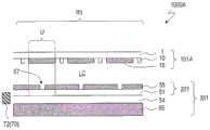
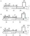
图1是示意性地示出本实施方式的扫描天线1000A的一部分的截面图,示意性地示出从设置于排列成同心圆状的缝隙的中心近旁的供电销72(参照图2的(b))起沿着半径方向的截面的一部分。FIG. 1 is a cross-sectional view schematically showing a part of a
扫描天线1000A具备TFT基板101A、缝隙基板201、配置在它们之间的液晶层LC、以及以隔着空气层54与缝隙基板201相对的方式配置的反射导电板65。扫描天线1000A从TFT基板101A侧发送、接收微波。The
TFT基板101A具有玻璃基板等电介质基板1、形成于电介质基板1上的多个贴片电极15、以及多个TFT10。各贴片电极15连接到对应的TFT10。各TFT10连接到栅极总线和源极总线。The
缝隙基板201具有玻璃基板等电介质基板51和形成于电介质基板51的液晶层LC侧的缝隙电极55。缝隙电极55具有多个缝隙57。The
反射导电板65配置成隔着空气层54与缝隙基板201相对。能够使用由相对于微波的介电常数M小的电介质(例如PTFE等氟树脂)形成的层来代替空气层54。缝隙电极55和反射导电板65以及它们之间的电介质基板51及空气层54作为波导301发挥功能。The reflective
贴片电极15、包含缝隙57的缝隙电极55的部分以及它们之间的液晶层LC构成天线单位U。在各天线单位U中,1个贴片电极15隔着液晶层LC与包含1个缝隙57的缝隙电极55的部分相对,构成液晶电容。另外,各天线单位U具有与液晶电容电并联连接的辅助电容(参照图3)。扫描天线1000A的天线单位U与LCD面板中的像素具有类似的构成。然而,扫描天线1000A与LCD面板具有许多不同之处。The
首先,扫描天线1000A的电介质基板1、51所要求的性能不同于LCD面板的基板所要求的性能。First, the performance required for the
LCD面板一般使用在可见光中透明的基板,例如使用玻璃基板或塑料基板。在反射型的LCD面板中,背面侧的基板不需要有透明性,因此有时也使用半导体基板。而作为天线用的电介质基板1、51,优选相对于微波的介电损耗(将相对于微波的介电损耗角正切表示为tanδM。)小。电介质基板1、51的tanδM优选为大致0.03以下,进一步优选为0.01以下。具体地,能使用玻璃基板或者塑料基板。玻璃基板与塑料基板相比尺寸稳定性、耐热性优异,适于使用LCD技术形成TFT、配线、电极等电路要素。例如在形成波导的材料是空气和玻璃的情况下,玻璃的上述介电损耗较大,因此从较薄的玻璃更能减小波导损耗这一观点来看,优选是400μm以下,更优选是300μm以下。没有特别的下限,只要在制造工艺中能无破损地进行处理即可。LCD panels generally use substrates that are transparent in visible light, such as glass substrates or plastic substrates. In a reflective LCD panel, the substrate on the back side does not need to have transparency, and therefore a semiconductor substrate is sometimes used. On the other hand, the
电极所使用的导电材料也是不同的。在LCD面板的像素电极、相对电极中多使用ITO膜作为透明导电膜。但是,ITO相对于微波的tanδM大,无法作为天线中的导电层使用。缝隙电极55与反射导电板65一起作为波导301的壁发挥功能。因而,为了抑制微波透射过波导301的壁,优选波导301的壁的厚度、即金属层(Cu层或者Al层)的厚度大。已知金属层的厚度若是表皮深度的3倍,则电磁波衰减为1/20(-26dB),若是5倍,则衰减为1/150(-43dB)左右。因而,若金属层的厚度是表皮深度的5倍,则能将电磁波的透射率降低为1%。例如,针对10GHz的微波,当使用厚度为3.3μm以上的Cu层和厚度为4.0μm以上的Al层时,能将微波降低到1/150。另外,当针对30GHz的微波使用厚度为1.9μm以上的Cu层和厚度为2.3μm以上的Al层时,能将微波降低到1/150。这样,优选缝隙电极55由比较厚的Cu层或者Al层形成。Cu层或者Al层的厚度没有特别的上限,可考虑成膜时间、成本而适当地设定。当使用Cu层时,能得到与使用Al层相比形成为较薄的优点。不仅能采用在LCD的制造工艺中使用的薄膜沉积法,还能采用将Cu箔或者Al箔贴附于基板等其它方法来形成比较厚的Cu层或者Al层。金属层的厚度例如是2μm以上30μm以下。在使用薄膜沉积法形成的情况下,优选金属层的厚度是5μm以下。此外,反射导电板65能使用厚度例如为几mm的铝板、铜板等。The conductive materials used for the electrodes are also different. ITO films are often used as transparent conductive films in pixel electrodes and opposite electrodes of LCD panels. However, ITO has a large tanδM with respect to microwaves, and cannot be used as a conductive layer in an antenna. The
贴片电极15并不是如缝隙电极55那样构成波导301,因此能使用与缝隙电极55相比厚度较小的Cu层或者Al层。但是,为了避免缝隙电极55的缝隙57附近的自由电子的振动诱发贴片电极15内的自由电子的振动时转化为热的损耗,而优选电阻低的贴片电极15。从批量生产性的观点来看,与Cu层相比优选使用Al层,优选Al层的厚度例如是0.3μm以上2μm以下。The
另外,天线单位U的排列间距与像素间距大为不同。例如,当考虑12GHz(Ku频带)的微波用的天线时,波长λ例如是25mm。这样,如专利文献4所记载的,天线单位U的间距是λ/4以下和/或λ/5以下,因此成为6.25mm以下和/或5mm以下。这比LCD面板的像素的间距大10倍以上。因而,天线单位U的长度和宽度也会比LCD面板的像素长度和宽度大约10倍。In addition, the arrangement pitch of the antenna units U is very different from the pixel pitch. For example, when considering an antenna for microwaves of 12 GHz (Ku band), the wavelength λ is, for example, 25 mm. In this way, as described in
当然,天线单位U的排列可与LCD面板中的像素的排列不同。在此,示出排列成同心圆状的例子(例如参照特开2002-217640号公报),但不限于此,例如也可以如非专利文献2所记载的那样排列成螺旋状。而且,也可以如专利文献4所记载的那样排列成矩阵状。Of course, the arrangement of the antenna units U may be different from the arrangement of the pixels in the LCD panel. Here, an example in which they are arranged in concentric circles is shown (for example, see Japanese Patent Laid-Open No. 2002-217640 ), but the invention is not limited to this. Furthermore, as described in
扫描天线1000A的液晶层LC的液晶材料所要求的特性与LCD面板的液晶材料所要求的特性不同。LCD面板通过像素的液晶层的折射率变化而对可见光(波长为380nm~830nm)的偏振光赋予相位差,从而使偏振状态变化(例如使直线偏振光的偏振轴方向旋转或者使圆偏振光的圆偏振度变化),由此进行显示。而实施方式的扫描天线1000A通过使天线单位U所具有的液晶电容的静电电容值变化而使从各贴片电极激振(再辐射)的微波的相位变化。因而,优选液晶层的相对于微波的介电常数M(εM)的各向异性(ΔεM)大,优选tanδM小。例如能适合使用在M.Wittek et al.,SID 2015DIGEST pp.824-826中记载的ΔεM为4以上且tanδM为0.02以下(均为19Gz的值)。除此之外,能使用在九鬼、高分子55卷8月号pp.599-602(2006)中记载的ΔεM为0.4以上、tanδM为0.04以下的液晶材料。The properties required for the liquid crystal material of the liquid crystal layer LC of the
液晶材料的介电常数一般具有频率分散性,但相对于微波的介电各向异性ΔεM与相对于可见光的折射率各向异性Δn存在正相关关系。因而可以说,就相对于微波的天线单位用的液晶材料而言,优选是相对于可见光的折射率各向异性Δn大的材料。LCD用的液晶材料的折射率各向异性Δn是用相对于550nm的光的折射率各向异性来评价的。当在此也将相对于550nm的光的Δn(双折射率)用作指标时,在针对微波的天线单位中使用Δn为0.3以上、优选为0.4以上的向列液晶。Δn没有特别的上限。不过,Δn大的液晶材料存在极性强的倾向,因此有可能使可靠性降低。从可靠性的观点来看,优选Δn是0.4以下。液晶层的厚度例如是1μm~500μm。The dielectric constant of liquid crystal materials generally has frequency dispersion, but there is a positive correlation between the dielectric anisotropy ΔεM with respect to microwaves and the refractive index anisotropy Δn with respect to visible light. Therefore, it can be said that a liquid crystal material for an antenna unit with respect to microwaves is preferably a material having a large refractive index anisotropy Δn with respect to visible light. The refractive index anisotropy Δn of the liquid crystal material for LCD was evaluated by the refractive index anisotropy with respect to light of 550 nm. When Δn (birefringence) with respect to light at 550 nm is also used here as an index, a nematic liquid crystal having Δn of 0.3 or more, preferably 0.4 or more, is used in the antenna unit for microwaves. Δn has no particular upper limit. However, since a liquid crystal material with a large Δn tends to have a strong polarity, reliability may be lowered. From the viewpoint of reliability, Δn is preferably 0.4 or less. The thickness of the liquid crystal layer is, for example, 1 μm to 500 μm.
以下,更详细地说明本发明的实施方式的扫描天线的结构和制造方法。Hereinafter, the structure and manufacturing method of the scanning antenna according to the embodiment of the present invention will be described in more detail.
(第1实施方式)(first embodiment)
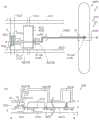
首先,参照图1和图2。图1如详述的那样是扫描天线1000A的中心附近的示意性局部截面图,图2的(a)和(b)分别是示出扫描天线1000A所具备的TFT基板101A和缝隙基板201的示意性俯视图。First, refer to FIGS. 1 and 2 . 1 is a schematic partial cross-sectional view of the vicinity of the center of the
扫描天线1000A具有按二维排列的多个天线单位U,在此例示的扫描天线1000A中,多个天线单位排列成同心圆状。在以下的说明中,将与天线单位U对应的TFT基板101A的区域和缝隙基板201的区域称为“天线单位区域”,标注与天线单位相同的附图标记U。另外,如图2的(a)和图2的(b)所示,在TFT基板101A和缝隙基板201中,将由按二维排列的多个天线单位区域划定的区域称为“发送接收区域R1”,将发送接收区域R1以外的区域称为“非发送接收区域R2”。在非发送接收区域R2中设置端子部、驱动电路等。The
图2的(a)是示出扫描天线1000A所具备的TFT基板101A的示意性俯视图。FIG. 2( a ) is a schematic plan view showing a
在图示的例子中,从TFT基板101A的法线方向观看时,发送接收区域R1是环状。非发送接收区域R2包含位于发送接收区域R1的中心部的第1非发送接收区域R2a和位于发送接收区域R1的周缘部的第2非发送接收区域R2b。发送接收区域R1的外径例如是200mm~1500mm,是根据通信量等设定的。In the example shown in the figure, when viewed from the normal direction of the
在TFT基板101A的发送接收区域R1中设置有由电介质基板1支撑的多个栅极总线GL和多个源极总线SL,利用这些配线来规定天线单位区域U。天线单位区域U在发送接收区域R1中排列成例如同心圆状。天线单位区域U各自包含TFT和电连接到TFT的贴片电极。TFT的源极电极电连接到源极总线SL,TFT的栅极电极电连接到栅极总线GL。另外,TFT的漏极电极与贴片电极电连接。A plurality of gate bus lines GL and a plurality of source bus lines SL supported by the
在非发送接收区域R2(R2a、R2b)中以包围发送接收区域R1的方式配置有密封区域Rs。对密封区域Rs赋予密封材料(未图示)。密封材料使TFT基板101A和缝隙基板201相互粘接,并且在这些基板101A、201之间封入液晶。In the non-transmission/reception area R2 (R2a, R2b), a sealing area Rs is arranged so as to surround the transmission/reception area R1. A sealing material (not shown) is provided to the sealing region Rs. The sealing material adheres the
在非发送接收区域R2中的密封区域Rs的外侧设置有栅极端子部GT、栅极驱动器GD、源极端子部ST以及源极驱动器SD。栅极总线GL各自经由栅极端子部GT连接到栅极驱动器GD。源极总线SL各自经由源极端子部ST连接到源极驱动器SD。此外,在该例中,源极驱动器SD和栅极驱动器GD形成于电介质基板1上,但这些驱动器中的一方或者双方也可以设置于另一电介质基板上。A gate terminal portion GT, a gate driver GD, a source terminal portion ST, and a source driver SD are provided outside the sealing region Rs in the non-transmission/reception region R2. The gate bus lines GL are each connected to the gate driver GD via the gate terminal portion GT. The source bus lines SL are each connected to the source drivers SD via the source terminal portions ST. In addition, in this example, the source driver SD and the gate driver GD are formed on the
在非发送接收区域R2中还设置有多个传输端子部PT。传输端子部PT与缝隙基板201的缝隙电极55(图2的(b))电连接。在本说明书中,将传输端子部PT与缝隙电极55的连接部称为“传输部”。如图所示,传输端子部PT(传输部)可以配置于密封区域Rs内。在该情况下,可以使用含有导电性粒子的树脂作为密封材料。由此,能使液晶封入TFT基板101A与缝隙基板201之间,并且能确保传输端子部PT与缝隙基板201的缝隙电极55的电连接。在该例中,在第1非发送接收区域R2a和第2非发送接收区域R2b两者中均配置有传输端子部PT,但也可以仅配置于任意一者。A plurality of transmission terminal portions PT are also provided in the non-transmission/reception area R2. The transmission terminal portion PT is electrically connected to the slit electrode 55 ( FIG. 2( b )) of the
此外,传输端子部PT(传输部)也可以不配置于密封区域Rs内。例如也可以配置于非发送接收区域R2中的密封区域Rs的外侧。In addition, the transmission terminal part PT (transmission part) may not be arrange|positioned in the sealing area|region Rs. For example, it may be arranged outside the sealing area Rs in the non-transmission/reception area R2.
图2的(b)是例示扫描天线1000A中的缝隙基板201的示意性俯视图,示出缝隙基板201的液晶层LC侧的表面。(b) of FIG. 2 is a schematic plan view illustrating the
在缝隙基板201中,在电介质基板51上,跨发送接收区域R1和非发送接收区域R2形成有缝隙电极55。In the
在缝隙基板201的发送接收区域R1中,多个缝隙57配置于缝隙电极55。缝隙57与TFT基板101A中的天线单位区域U对应配置。在图示的例子中,多个缝隙57为了构成径向线缝隙天线,而使在相互大致正交的方向上延伸的一对缝隙57排列成同心圆状。由于具有相互大致正交的缝隙,因此扫描天线1000A能发送、接收圆偏振波。In the transmission/reception region R1 of the
缝隙电极55的端子部IT在非发送接收区域R2中设置有多个。端子部IT与TFT基板101A的传输端子部PT(图2的(a))电连接。在该例中,端子部IT配置于密封区域Rs内,通过含有导电性粒子的密封材料与对应的传输端子部PT电连接。A plurality of terminal portions IT of the
另外,在第1非发送接收区域R2a中,供电销72配置于缝隙基板201的背面侧。微波通过供电销72进入由缝隙电极55、反射导电板65以及电介质基板51构成的波导301。供电销72连接到供电装置70。从排列有缝隙57的同心圆的中心进行供电。供电的方式可以是直接连结供电方式和电磁耦合方式中的任意一种,能采用公知的供电结构。In addition, in the first non-transmission/reception region R2a, the feeding pins 72 are arranged on the back side of the
在图2的(a)和(b)中,示出了密封区域Rs以将包含发送接收区域R1的比较窄的区域包围的方式设置的例子,但不限于此。特别是,设置于发送接收区域R1的外侧的密封区域Rs也可以是以与发送接收区域R1之间具有一定距离以上的方式设置于例如电介质基板1和/或电介质基板51的边的近旁。当然,设置于非发送接收区域R2的、例如端子部或驱动电路也可以形成于密封区域Rs的外侧(即,不存在液晶层的一侧)。通过在与发送接收区域R1相隔一定距离以上的位置形成密封区域Rs,由此,能够抑制受到密封材料(特别是固化性树脂)中包含的杂质(特别是离子性杂质)的影响而致使天线特性下降。In (a) and (b) of FIG. 2 , an example in which the sealing region Rs is provided so as to surround a relatively narrow region including the transmission/reception region R1 is shown, but it is not limited to this. In particular, the sealing region Rs provided outside the transmission/reception area R1 may be provided in the vicinity of the sides of the
以下,参照附图更详细地说明扫描天线1000A的各构成要素。Hereinafter, each constituent element of the
<TFT基板101A的结构><Configuration of
·天线单位区域UAntenna unit area U
参照图3说明本实施方式的扫描天线1000A和扫描天线1000A所具备的TFT基板101A。The
图3的(a)是扫描天线1000A的发送接收区域R1的天线单位区域U的示意性俯视图,图3的(b)是沿着图3的(a)中的A-A’线的TFT基板101A的示意性截面图。FIG. 3( a ) is a schematic plan view of the antenna unit region U of the transmission/reception region R1 of the
如图3的(a)和图3的(b)所示,TFT基板101A具有电介质基板1和在电介质基板1上排列的多个天线单位区域U。多个天线单位区域U各自具有:TFT10;贴片电极15,其电连接到TFT10的漏极电极7D;以及贴片漏极连接部,其将漏极电极7D和贴片电极15电连接。贴片漏极连接部包含导电部,该导电部包含于导电层,该导电层是比包含贴片电极15的导电层15l靠近电介质基板1的导电层,并且是包含TFT10的栅极电极3G的导电层3和包含TFT10的源极电极7S的导电层7中的任意的更靠近电介质基板1的一方导电层。在TFT基板101A中,包含TFT10的栅极电极3G的栅极金属层3和包含TFT10的源极电极7S的源极金属层7中的栅极金属层3更靠近电介质基板1。TFT基板101A的贴片漏极连接部包含栅极金属层3所包含的配线3w1。As shown in FIGS. 3( a ) and 3 ( b ), the
在本说明书中,各天线单位区域的“贴片漏极连接部”是指与漏极电极和贴片电极电连接并配置在漏极电极与贴片电极之间的至少1个导电部。漏极电极与贴片电极经由贴片漏极连接部电连接。例如,在图3所示的TFT基板101A中,漏极电极7D与贴片电极15经由连接部15a1、15a2和3a2以及配线3w1电连接。TFT基板101A所具有的贴片漏极连接部包含连接部15a1、15a2和3a2以及配线3w1。In this specification, the "patch drain connection portion" of each antenna unit region refers to at least one conductive portion that is electrically connected to the drain electrode and the patch electrode and arranged between the drain electrode and the patch electrode. The drain electrode and the chip electrode are electrically connected through the chip drain connection part. For example, in the
配线3w1在从TFT基板101A和缝隙基板201的法线方向观看时在缝隙57内在缝隙57的长轴方向上延伸,在缝隙57内与贴片电极15重叠。The wiring 3w1 extends in the longitudinal direction of the
在本说明书中,有时将使用栅极用导电膜形成的包含栅极电极3G的层(layer)称为“栅极金属层”,有时将使用源极用导电膜形成的包含源极电极7S的层称为“源极金属层”。另外,有时将由贴片用导电膜形成的包含贴片电极15的层称为“贴片金属层”。在本实施方式中,贴片电极15包含于与包含TFT10的栅极电极3G的导电层和包含TFT10的源极电极7S的导电层均不同的导电层。In this specification, the layer including the
具备TFT基板101A的扫描天线1000A与图5所示的参考例1的扫描天线1001R相比具有优异的天线性能。参照图4~图6说明扫描天线1000A所具有的优点。The
如上所述,扫描天线通过控制施加到天线单位的各液晶层的电压,使各天线单位的液晶层的有效的介电常数M(εM)变化,从而以静电电容不同的天线单位形成二维的图案。本发明的发明人通过种种研究,发现了使天线性能降低的新的重要因素。本发明的发明人发现,当包含贴片电极15的贴片金属层15l在缝隙57的内侧和近旁包含贴片电极15以外的导电部时,扫描天线的天线性能会降低。以下,详细说明该重要因素。As described above, the scanning antenna controls the voltage applied to each liquid crystal layer of the antenna unit to change the effective dielectric constant M (εM ) of the liquid crystal layer of each antenna unit, thereby forming two-dimensional antenna units with different electrostatic capacitances picture of. The inventors of the present invention have discovered a new important factor that degrades the antenna performance through various studies. The inventors of the present invention found that when the
首先,参照图4说明在扫描天线1000A的贴片电极15和缝隙57近旁的液晶分子的取向。图4的(a)是用于说明扫描天线1000A的贴片金属层15l与缝隙57的位置关系的示意性俯视图,图4的(b)和图4的(c)分别是沿着图4的(a)中的X-X’线和Y-Y’线的扫描天线1000A的示意性截面图。图4的(a)中的X-X’线和Y-Y’线分别兼作缝隙57的长轴AS和短轴BS。First, the alignment of the liquid crystal molecules in the vicinity of the
对天线性能特别有影响的是在从TFT基板101A和缝隙基板201的法线方向观看时贴片电极15与缝隙电极55重叠的交叠区域Ro(图4的(a)中的斜线部)。如图4的(a)所示,在从TFT基板101A和缝隙基板201的法线方向观看时,缝隙57的短轴BS方向的长度ws比贴片电极15的在缝隙57的短轴BS方向的长度wp小。由此,形成了交叠区域Ro。在本说明书中,将在从TFT基板和缝隙基板的法线方向观看时贴片电极与缝隙电极重叠的区域称为“交叠区域”。What has a particular influence on the antenna performance is the overlapping region Ro where the
从天线性能的观点来说,优选交叠区域Ro具有相对于缝隙57的长轴AS为线对称的平面形状。即,优选2个交叠区域Ro配置成相对于缝隙57的长轴AS为线对称。进一步优选交叠区域Ro具有相对于缝隙57的短轴BS也为线对称的平面形状。即,进一步优选2个交叠区域Ro各自具有相对于缝隙57的短轴BS也为线对称的平面形状。From the viewpoint of antenna performance, it is preferable that the overlapping region Ro has a plane shape that is line-symmetric with respect to the long axis AS of the
图4的(b)和图4的(c)示意性地示出交叠区域Ro中的施加电压时的液晶分子(介电各向异性为正)的取向状态。对于交叠区域Ro以外的液晶分子的取向状态省略了图示,但是与交叠区域Ro内的液晶分子连续地取向。交叠区域Ro以外的区域(即,在从TFT基板101A和缝隙基板201的法线方向观看时,贴片电极15与缝隙电极55不重叠的区域)的液晶分子的取向也受到由贴片电极15和缝隙电极55形成的电场的影响。另外,还受到TFT基板101A的表面形状(液晶层LC侧的表面形状)的影响。FIGS. 4( b ) and 4 ( c ) schematically show alignment states of liquid crystal molecules (with positive dielectric anisotropy) when a voltage is applied in the overlapping region Ro. Although illustration is abbreviate|omitted about the orientation state of the liquid crystal molecules outside the overlapping region Ro, it is aligned continuously with the liquid crystal molecules in the overlapping region Ro. The orientation of the liquid crystal molecules in the regions other than the overlapping region Ro (that is, the region where the
当如参照图5、图6以及图7后述的参考例的扫描天线那样,贴片金属层15l在缝隙57的内侧和/或近旁包含贴片电极15以外的导电部时,该导电部会对贴片电极15和缝隙57近旁的液晶分子的取向(包含交叠区域Ro的液晶分子的取向)造成影响。由此,天线性可能会降低。As in the scanning antenna of the reference example described later with reference to FIGS. 5 , 6 , and 7 , when the
此外,主要对天线性能作出贡献的是在缝隙57的内侧和/或近旁包含于贴片金属层15l的除贴片电极15以外的导电部。因此,仅就天线性能而言,即使是包含于贴片金属层15l的除贴片电极15以外的导电部,若该导电部是远离缝隙57和贴片电极15而形成的,则也能将该导电部忽略。例如,在TFT基板101A中,如图3的(a)所示,贴片金属层15l在天线单位区域U中还包含连接部15a1和15a2,但是它们远离缝隙57和贴片电极15而形成的,因此对天线性能的贡献小。这样,优选包含于贴片金属层15l的除贴片电极15以外的导电部配置为与缝隙57和贴片电极15隔开一定距离以上。In addition, what mainly contributes to the antenna performance is the conductive portion other than the
在从TFT基板101A和缝隙基板201的法线方向观看时,贴片金属层15l在缝隙57的内侧和近旁不包含贴片电极15以外的导电部。因此,扫描天线1000A具有优异的天线性能。When viewed from the normal direction of the
而且,扫描天线1000A的交叠区域Ro具有相对于缝隙57的长轴AS为线对称的平面形状,具有相对于缝隙57的短轴BS也为线对称的平面形状。Furthermore, the overlapping region Ro of the
缝隙57例如如图所示是用半圆置换了长方形的沿着长轴AS的两端的形状,但是不限于此。例如,也可以是长方形,还可以是长方形的角带有圆度的形状。For example, as shown in the figure, the
接下来,参照图5和图6说明参考例1的扫描天线1001R。图5的(a)是参考例1的扫描天线1001R的发送接收区域R1的天线单位区域U的示意性俯视图,图5的(b)是参考例1的扫描天线1001R所具备的TFT基板101R的沿着图5的(a)中的A-A’线的示意性截面图。图6的(a)是用于说明参考例1的扫描天线1001R的贴片金属层15l与缝隙57的位置关系的示意性俯视图,图6的(b)和图6的(c)分别是沿着图6的(a)中的X-X’线和Y-Y’线的参考例1的扫描天线1001R的示意性截面图。在图5和图6中,对与先前的附图共同的构成要素标注共同的附图标记,避免重复说明。Next, the
如图5的(a)和图5的(b)所示,参考例1的扫描天线1001R与扫描天线1000A的不同之处在于贴片漏极连接部。参考例1的扫描天线1001R所具备的TFT基板101R的贴片漏极连接部包含贴片金属层15l所包含的配线15w1。配线15w1在从TFT基板101R和缝隙基板201的法线方向观看时在缝隙57内在缝隙57的长轴AS方向上延伸。配线15w1与贴片电极15一体地形成。即,贴片金属层15l在缝隙57的内侧和近旁包含贴片电极15以外的导电部。在图6的(a)中,对在缝隙57的内侧和近旁包含于贴片金属层15l的除贴片电极15以外的导电部标注与交叠区域Ro不同的影线。As shown in FIGS. 5( a ) and 5 ( b ), the
由于贴片金属层15l在缝隙57的内侧和近旁包含贴片电极15以外的导电部,从而参考例1的扫描天线1001R在天线性能上比扫描天线1000A差。The
在图6的(b)和图6的(c)中,不仅图示了交叠区域Ro中的液晶分子的取向状态,也图示了贴片金属层15l(贴片电极15以外)与缝隙电极55重叠的区域中的液晶分子的取向状态(图中用虚线的圆示出)。由于存在配线15w1,该区域的液晶分子的取向会强烈地受到电场的影响。另外,在缝隙57内,TFT基板101R的表面有台阶。因此,在参考例1的扫描天线1001R中,液晶分子的取向状态比图4所示的扫描天线1000A差。此外,与交叠区域的液晶分子的取向相比,交叠区域Ro以外的区域(即,在从TFT基板101A和缝隙基板201的法线方向观看时贴片电极15与缝隙电极55不重叠的区域)的液晶分子的取向有易于受到配线15w1的影响的趋势。In FIGS. 6(b) and 6(c) , not only the alignment state of the liquid crystal molecules in the overlapping region Ro, but also the chip metal layer 151 (other than the chip electrode 15 ) and the gap are shown. The alignment state of the liquid crystal molecules in the region where the
由于贴片金属层15l在缝隙57的内侧和/或近旁包含贴片电极15以外的导电部而天线性能差这一问题有时在贴片金属层15l比较厚的情况下是显著的。因此,在具有比较厚的贴片金属层的扫描天线中,通过使贴片金属层15l在缝隙57的内侧和近旁不包含贴片电极15以外的导电部,从而抑制天线性能低的效果大。The problem that the antenna performance is poor because the
天线性能差的问题并不限于在参考例1的扫描天线1001R中产生。例如,在图7的(a)所示的参考例2的扫描天线1002R中,也会产生天线性能差的问题。The problem of poor antenna performance is not limited to occurring in the
图7的(a)是用于说明参考例2的扫描天线1002R的贴片金属层15l与缝隙57的位置关系的示意性俯视图,图7的(b)和图7的(c)分别是沿着图7的(a)中的X-X’线和Y-Y’线的参考例2的扫描天线1002R的示意性截面图。在图7中,对与先前的附图共同的构成要素标注共同的附图标记。7( a ) is a schematic plan view for explaining the positional relationship between the
如图7的(a)所示,参考例2的扫描天线1002R所具备的TFT基板的贴片漏极连接部包含贴片金属层15l所包含的配线15w2。配线15w2在缝隙57的短轴BS方向上延伸,与贴片电极15一体地形成。配线15w2在沿缝隙57的短轴BS方向延伸这一点上与参考例1的扫描天线1001R所具有的配线15w1不同。在参考例2的扫描天线1002R中,贴片金属层15l在缝隙57的近旁包含贴片电极15以外的导电部。因此,与扫描天线1000A相比天线性能差。As shown in FIG. 7( a ), the chip drain connection portion of the TFT substrate included in the scan antenna 1002R of Reference Example 2 includes the wiring 15w2 included in the
此外,参考例2的扫描天线1002R与参考例1的扫描天线1001R相比有时天线性能也差。如图7的(a)和图7的(c)所示,参考例2的扫描天线1002R的配线15w2与交叠区域Ro相邻地配置。因此,这会导致交叠区域Ro中的液晶分子的取向状态易于被由配线15w2引起的电场影响。In addition, the scanning antenna 1002R of Reference Example 2 may have inferior antenna performance as compared with the
更详细地说明TFT基板101A的天线单位区域U的结构。再次参照图3的(a)和图3的(b)。The structure of the antenna unit region U of the
如图3所示,TFT基板101A具有:栅极金属层3,其支撑于电介质基板1;栅极绝缘层4,其形成在栅极金属层3上;源极金属层7,其形成在栅极绝缘层4上;第1绝缘层11,其形成在源极金属层7上;贴片金属层15l,其形成在第1绝缘层11上;以及第2绝缘层17,其形成在贴片金属层15l上。如参照图8~图10后述的那样,TFT基板101A还具有形成在第1绝缘层11与贴片金属层15l之间的下部导电层13。TFT基板101A还具有形成在第2绝缘层17上的上部导电层19。As shown in FIG. 3, the
各天线单位区域U所具有的TFT10具备栅极电极3G、岛状的半导体层5、接触层6S和6D、配置在栅极电极3G与半导体层5之间的栅极绝缘层4、以及源极电极7S和漏极电极7D。在该例子中,TFT10是具有底栅结构的沟道蚀刻型的TFT。The
栅极电极3G电连接到栅极总线GL,从栅极总线GL被供应扫描信号电压。源极电极7S电连接到源极总线SL,从源极总线SL被供应数据信号电压。在该例子中,栅极电极3G和栅极总线GL由相同导电膜(栅极用导电膜)形成。在此,源极电极7S、漏极电极7D以及源极总线SL由相同导电膜(源极用导电膜)形成。栅极用导电膜和源极用导电膜例如是金属膜。The
半导体层5以隔着栅极绝缘层4与栅极电极3G重叠的方式配置。在图示的例子中,在半导体层5上形成有源极接触层6S和漏极接触层6D。源极接触层6S和漏极接触层6D分别配置在半导体层5中的形成沟道的区域(沟道区域)的两侧。也可以是,半导体层5是本征非晶硅(i-a-Si)层,源极接触层6S和漏极接触层6D是n+型非晶硅(n+-a-Si)层。The
源极电极7S以与源极接触层6S接触的方式设置,经由源极接触层6S连接到半导体层5。漏极电极7D以与漏极接触层6D接触的方式设置,经由漏极接触层6D连接到半导体层5。The
在此,各天线单位区域U具有与液晶电容电并联连接的辅助电容。在该例子中,辅助电容包括:上部辅助电容电极(有时称为“辅助电容电极”。)7C,其与漏极电极7D电连接;栅极绝缘层4;以及下部辅助电容电极(有时称为“辅助电容相对电极”。)3C,其隔着栅极绝缘层4与上部辅助电容电极7C相对。下部辅助电容电极3C包含于栅极金属层3,上部辅助电容电极7C包含于源极金属层7。栅极金属层3还包含连接到下部辅助电容电极3C的CS总线(辅助电容线)CL。CS总线CL例如与栅极总线GL大致平行地延伸。在该例子中,下部辅助电容电极3C与CS总线CL一体地形成。下部辅助电容电极3C的宽度可以比CS总线CL的宽度大。另外,在该例子中,上部辅助电容电极7C从漏极电极7D延伸设置。上部辅助电容电极7C的宽度可以比从漏极电极7D延伸设置的部分中的上部辅助电容电极7C以外的部分的宽度大。此外,辅助电容和贴片电极15的配置关系不限于图示的例子。Here, each antenna unit region U has an auxiliary capacitor electrically connected in parallel with the liquid crystal capacitor. In this example, the auxiliary capacitor includes: an upper auxiliary capacitor electrode (sometimes referred to as "auxiliary capacitor electrode".) 7C, which is electrically connected to the
栅极金属层3包含TFT10的栅极电极3G、栅极总线GL、下部辅助电容电极3C以及CS总线CL。栅极金属层3还包含:连接部3a2,其与栅极电极3G是电分离的;以及配线3w1,其与连接部3a2一体地形成。The
栅极绝缘层4具有:开口部4a2,其到达连接部3a2;以及开口部4a3,其到达配线3w1。开口部4a3在从电介质基板1的法线方向观看时与贴片电极15重叠。The
源极金属层7包含TFT10的源极电极7S和漏极电极7D、源极总线SL、以及上部辅助电容电极7C。The
第1绝缘层11以覆盖TFT10的方式形成。第1绝缘层11具有:开口部11a1,其到达漏极电极7D或从漏极电极7D延伸设置的部分;开口部11a2,其在从电介质基板1的法线方向观看时与开口部4a2重叠;以及开口部11a3,其在从电介质基板1的法线方向观看时与开口部4a3重叠。有时将开口部11a1称为接触孔CH_a1。形成于栅极绝缘层4的开口部4a2和形成于第1绝缘层11的开口部11a2构成接触孔CH_a2。形成于栅极绝缘层4的开口部4a3和形成于第1绝缘层11的开口部11a3构成接触孔CH_a3。The first insulating
贴片金属层15l包含贴片电极15、以及连接部15a1和15a2。The
连接部15a1形成在第1绝缘层11上和开口部11a1内,在开口部11a1内与漏极电极7D或从漏极电极7D延伸设置的部分连接。例如在此,连接部15a1在开口部11a1内与从漏极电极7D延伸设置的部分接触。The connection portion 15a1 is formed on the first insulating
连接部15a2与连接部15a1一体地连接。连接部15a2形成在第1绝缘层11上和接触孔CH_a2内,在接触孔CH_a2内与连接部3a2连接。例如在此,连接部15a2在形成于栅极绝缘层4的开口部4a2内与连接部3a2接触。The connection part 15a2 is integrally connected to the connection part 15a1. The connection portion 15a2 is formed on the first insulating
贴片电极15形成在第1绝缘层11上和接触孔CH_a3内,在接触孔CH_a3内与配线3w1连接。例如在此,贴片电极15在形成于栅极绝缘层4的开口部4a3内与配线3w1接触。The
贴片金属层15l包含金属层。贴片金属层15l也可以仅由金属层形成。贴片金属层15l例如具有具备低电阻金属层和位于低电阻金属层之下的含高熔点金属的层的层叠结构。层叠结构也可以在低电阻金属层之上还具有含高熔点金属的层。“含高熔点金属的层”是包含从包括钛(Ti)、钨(W)、钼(Mo)、钽(Ta)以及铌(Nb)的组中选择的至少1种元素的层。“含高熔点金属的层”也可以是层叠结构。例如,含高熔点金属的层是指由Ti、W、Mo、Ta、Nb、包含它们的合金及它们的氮化物、以及上述金属或者合金与上述氮化物的固溶体中的任意一者形成的层。“低电阻金属层”是包含从包括铜(Cu)、铝(Al)、银(Ag)以及金(Au)的组中选择的至少1种元素的层。“低电阻金属层”也可以是层叠结构。有时将贴片金属层15l的低电阻金属层称为“主层”,有时将低电阻金属层之下和之上的含高熔点金属的层分别称为“下层”和“上层”。The
贴片金属层15l例如包含Cu层或Al层作为主层。即,贴片电极15例如包含Cu层或Al层作为主层。扫描天线的性能与贴片电极15的电阻相关,主层的厚度设定为能得到期望的电阻。从电阻的观点来说,存在Cu层相比于Al层更能减小贴片电极15的厚度的可能性。贴片金属层15l所具有的金属层的厚度(即,贴片电极15所具有的金属层的厚度)例如设定为比源极电极7S和漏极电极7D的厚度大。在贴片电极15中的金属层由Al层形成的情况下,贴片电极15中的金属层的厚度例如设定为0.3μm以上。The
第2绝缘层17以覆盖贴片电极15、连接部15a1和15a2的方式形成。The second insulating
在图示的例子中,TFT基板101A具有多个接触孔CH_a3。贴片电极15经由多个接触孔CH_a3与配线3w1连接。但是,接触孔的个数、形状不限于图示的例子,接触孔CH_a3只要设置有1个以上即可。根据本发明的发明人的研究,通过使TFT基板101A具有多个接触孔CH_a3,能得到以下的优点。当在接触孔CH_a3内贴片金属层15l与栅极金属层3接触的面积的总计值变大时,能提高贴片金属层15l与栅极金属层3的紧贴性。另外,在接触面积相同的情况下,多个接触孔CH_a3的边缘的长度之和越大,越能降低贴片金属层15l与栅极金属层3之间的接触电阻。例如,在栅极金属层3具有具备低电阻金属层和位于低电阻金属层之上的含高熔点金属的层(上层)的层叠结构的情况下,在对第1绝缘膜11和栅极绝缘膜4进行蚀刻来形成接触孔CH_a3的工序中,栅极金属层3的上层的一部分也同时被蚀刻。栅极金属层3的上层残留为沿着接触孔CH_a3的边缘的环状,该环状的栅极金属层3的上层与贴片金属层15l的接触有助于电接触。因此,当多个接触孔CH_a3的边缘的长度之和大时,栅极金属层3与贴片金属层15l之间的接触电阻会降低。In the illustrated example, the
其它接触孔(例如接触孔CH_a2)也同样不限于图示的例子,也可以设置有多个。通过具有多个接触孔,能得到上述的优点。The other contact holes (eg, the contact holes CH_a2 ) are also not limited to the example shown in the figure, and a plurality of them may be provided. By having a plurality of contact holes, the above-mentioned advantages can be obtained.
从天线性能的观点来说,优选接触孔CH_a3具有相对于缝隙57的长轴为线对称的平面形状。进一步优选接触孔CH_a3具有相对于缝隙57的短轴也为线对称的平面形状。例如,优选多个接触孔CH_a3配置成相对于缝隙57的长轴为线对称,进一步优选配置成相对于缝隙57的短轴为线对称。From the viewpoint of antenna performance, it is preferable that the contact hole CH_a3 has a plane shape that is line-symmetric with respect to the long axis of the
TFT基板101A的贴片漏极连接部也可以如下描述。TFT基板101A的贴片漏极连接部具有:导电部,其包含于比包含贴片电极15的导电层15l靠近电介质基板1的导电层;以及另外的导电部15a1和15a2,其包含于包含贴片电极15的导电层15l,与贴片电极15在物理上分离地形成。TFT基板101A的贴片漏极连接部具有:配线3w1,其包含于比包含贴片电极15的贴片金属层15l靠近电介质基板1的栅极金属层3;以及连接部15a1和15a2,其包含于包含贴片电极15的贴片金属层15l,与贴片电极15在物理上分离地形成。配线3w1包含于包含TFT10的栅极电极3G的导电层3和包含TFT10的源极电极7S的导电层7中的任意的更靠近电介质基板1的一方导电层。在TFT基板101A中,包含TFT10的栅极电极3G的栅极金属层3和包含TFT10的源极电极7S的源极金属层7中的栅极金属层3更靠近电介质基板1。The chip drain connection portion of the
由于TFT基板101A具有另外的导电部15a1和15a2,另外的导电部15a1和15a2包含于包含贴片电极15的导电层15l,与贴片电极15在物理上分离地形成,从而还能得到以下的优点。贴片用导电膜15’的蚀刻工序中的蚀刻量降低,因此贴片用导电膜15’的蚀刻剂能长寿命化。另外,能削减具备TFT基板101A的扫描天线1000A的液晶层的体积(即液晶材料的体积),降低扫描天线1000A的成本。Since the
此外,本实施方式不限于图示的例子。例如,TFT的结构不限于图示的例子,栅极金属层3与源极金属层7的配置关系也可以是相反的。TFT也可以具有顶栅结构。也可以是,包含TFT的源极电极的导电层比包含TFT的栅极电极的导电层靠近电介质基板。也可以是,贴片漏极连接部包含导电部,该导电部包含于导电层,该导电层是比包含贴片电极的导电层靠近电介质基板的导电层,并且是包含TFT的栅极电极的导电层和包含TFT的源极电极的导电层中的任意的更靠近电介质基板的一方导电层。In addition, this embodiment is not limited to the example shown in figure. For example, the structure of the TFT is not limited to the illustrated example, and the arrangement relationship of the
参照图8~图10说明TFT基板101A的非发送接收区域R2的结构。但是,TFT基板101A的非发送接收区域R2的结构不限于图示的例子。扫描天线1000A基本上无论非发送接收区域R2的结构如何都能如上所述具有优异的天线性能。The structure of the non-transmission/reception region R2 of the
图8的(a)和图8的(b)是TFT基板101A的非发送接收区域R2的示意性俯视图,图9的(a)~(d)和图10的(a)~(c)分别是TFT基板101A的非发送接收区域R2的示意性截面图。图8的(a)示出设置于非发送接收区域R2的源极-栅极连接部SG和源极端子部ST,图8的(b)示出设置于非发送接收区域R2的传输端子部PT、栅极端子部GT以及CS端子部CT。FIGS. 8( a ) and 8 ( b ) are schematic plan views of the non-transmission/reception region R2 of the
传输端子部PT包含:第1传输端子部PT1,其位于密封区域Rs;以及第2传输端子部PT2,其设置在密封区域Rs的外侧(没有液晶层的一侧)。在图示的例子中,第1传输端子部PT1沿着密封区域Rs以包围发送接收区域R1的方式延伸。The transmission terminal portion PT includes a first transmission terminal portion PT1 located in the sealing region Rs, and a second transmission terminal portion PT2 provided outside the sealing region Rs (the side without the liquid crystal layer). In the illustrated example, the first transmission terminal portion PT1 extends along the sealing region Rs so as to surround the transmission/reception region R1.
图9的(a)示出沿着图8的(b)中的B-B’线的第1传输端子部PT1的截面,图9的(b)示出沿着图8的(a)中的C-C’线的源极-栅极连接部SG的截面,图9的(c)示出沿着图8的(a)中的D-D’线的源极端子部ST的截面,图9的(d)示出沿着图8的(b)中的E-E’线的第2传输端子部PT2的截面,图10的(a)示出沿着图8的(b)中的F-F’线的第1传输端子部PT1的截面,图10的(b)示出沿着图8的(a)中的G-G’线的源极-栅极连接部SG的截面,图10的(c)示出沿着图8的(a)中的H-H’线的源极-栅极连接部SG和源极端子部ST的截面。FIG. 9( a ) shows a cross section of the first transmission terminal portion PT1 along the line BB′ in FIG. 8( b ), and FIG. 9( b ) shows a The cross-section of the source-gate connection portion SG along the CC' line, Fig. 9(c) shows the cross-section of the source terminal portion ST along the DD' line in Fig. 8(a), FIG. 9( d ) shows a cross section of the second transmission terminal portion PT2 along the line EE′ in FIG. 8( b ), and FIG. 10( a ) shows the 10(b) shows a cross-section of the source-gate connection portion SG along the GG' line in FIG. 8(a) 10(c) shows a cross section of the source-gate connection portion SG and the source terminal portion ST along the H-H' line in Fig. 8(a) .
一般地,栅极端子部GT和源极端子部ST分别按每个栅极总线和每个源极总线设置。另外,源极-栅极连接部SG一般与各源极总线对应地设置。在图8的(b)中,与栅极端子部GT并排地图示有CS端子部CT和第2传输端子部PT2,但CS端子部CT和第2传输端子部PT2的个数和配置是分别与栅极端子部GT独立地设定的。通常,CS端子部CT和第2传输端子部PT2的个数比栅极端子部GT的个数少,并考虑CS电极和缝隙电极的电压的均匀性而适当地设定。另外,在形成有第1传输端子部PT1的情况下,第2传输端子部PT2可省略。Generally, the gate terminal portion GT and the source terminal portion ST are provided for each gate bus line and each source bus line, respectively. In addition, the source-gate connection part SG is generally provided corresponding to each source bus line. In (b) of FIG. 8 , the CS terminal portion CT and the second transfer terminal portion PT2 are shown in parallel with the gate terminal portion GT, but the number and arrangement of the CS terminal portion CT and the second transfer terminal portion PT2 are different from each other. It is set independently of the gate terminal GT. Usually, the numbers of CS terminal portions CT and second transfer terminal portions PT2 are smaller than the number of gate terminal portions GT, and are appropriately set in consideration of the uniformity of the voltages between the CS electrodes and the slit electrodes. In addition, when the 1st transmission terminal part PT1 is formed, the 2nd transmission terminal part PT2 can be abbreviate|omitted.
各CS端子部CT例如与各CS总线对应地设置。各CS端子部CT也可以与多个CS总线对应地设置。例如,在对各CS总线供应与缝隙电压相同的电压的情况下,TFT基板101A只要具有至少1个CS端子部CT即可。但是,为了降低配线电阻,优选TFT基板101A具有多个CS端子部CT。此外,缝隙电压例如是接地电位。另外,在对CS总线供应与缝隙电压相同的电压的情况下,可省略CS端子部CT或第2传输端子部PT2中的任意一者。Each CS terminal part CT is provided corresponding to each CS bus line, for example. Each CS terminal portion CT may be provided corresponding to a plurality of CS bus lines. For example, when the same voltage as the slit voltage is supplied to each CS bus line, the
·源极-栅极连接部SG· Source-gate connection SG
如图8的(a)所示,TFT基板101A在非发送接收区域R2具有源极-栅极连接部SG。源极-栅极连接部SG一般按每个源极总线SL设置。源极-栅极连接部SG将各源极总线SL电连接到形成在栅极金属层3内的连接配线(有时称为“源极下部连接配线”。)。As shown in FIG. 8( a ), the
如图8的(a)、图9的(b)、图10的(b)和图10的(c)所示,源极-栅极连接部SG具有:源极下部连接配线3sg;开口部4sg1,其形成于栅极绝缘层4;源极总线连接部7sg;开口部11sg1和开口部11sg2,其形成于第1绝缘层11;以及源极总线上部连接部13sg。As shown in FIGS. 8( a ), 9 ( b ), 10 ( b ), and 10 ( c ), the source-gate connection portion SG has: a source lower connection wiring 3sg; an opening A portion 4sg1 formed in the
源极下部连接配线3sg包含于栅极金属层3。源极下部连接配线3sg是与栅极总线GL电分离的。The source lower connection wiring 3sg is included in the
形成于栅极绝缘层4的开口部4sg1到达源极下部连接配线3sg。The opening 4sg1 formed in the
源极总线连接部7sg包含于源极金属层7,电连接到源极总线SL。在该例子中,源极总线连接部7sg从源极总线SL延伸设置,与源极总线SL一体地形成。源极总线连接部7sg的宽度可以比源极总线SL的宽度大。The source bus line connecting portion 7sg is included in the
形成于第1绝缘层11的开口部11sg1在从电介质基板1的法线方向观看时与形成于栅极绝缘层4的开口部4sg1重叠。形成于栅极绝缘层4的开口部4sg1和形成于第1绝缘层11的开口部11sg1构成接触孔CH_sg1。The opening 11sg1 formed in the first insulating
形成于第1绝缘层11的开口部11sg2到达源极总线连接部7sg。有时将开口部11sg2称为接触孔CH_sg2。The opening portion 11sg2 formed in the first insulating
源极总线上部连接部13sg(有时简称为“上部连接部13sg”。)包含于下部导电层13。上部连接部13sg形成在第1绝缘层11上、接触孔CH_sg1内以及接触孔CH_sg2内,在接触孔CH_sg1内与源极下部连接配线3sg连接,在接触孔CH_sg2内与源极总线连接部7sg连接。例如在此,上部连接部13sg在形成于栅极绝缘层4的开口部4sg1内与源极下部连接配线3sg接触,在形成于第1绝缘层11的开口部11sg2内与源极总线连接部7sg接触。The source bus line upper connecting portion 13sg (sometimes abbreviated as “the upper connecting portion 13sg”) is included in the lower
优选源极下部连接配线3sg中的通过开口部4sg1露出的部分被上部连接部13sg覆盖。优选源极总线连接部7sg中的通过开口部11sg2露出的部分被上部连接部13sg覆盖。It is preferable that a portion of the source lower connection wiring 3sg exposed through the opening portion 4sg1 is covered by the upper connection portion 13sg. It is preferable that the part exposed by the opening part 11sg2 in the source bus line connection part 7sg is covered with the upper connection part 13sg.
下部导电层13例如包含透明导电层(例如ITO层)。The lower
在该例子中,源极-栅极连接部SG不具有包含于贴片金属层15l的导电部和包含于上部导电层19的导电部。In this example, the source-gate connection portion SG does not have the conductive portion included in the
TFT基板101A通过在源极-栅极连接部SG具有上部连接部13sg,从而具有优异的动作稳定性。通过使源极-栅极连接部SG具有上部连接部13sg,从而对用于形成贴片金属层15l的贴片用导电膜进行蚀刻的工序中的、对栅极金属层3和/或源极金属层7的损伤得以减轻。说明该效果。The
如上所述,在TFT基板101A中,源极-栅极连接部SG不具有包含于贴片金属层15l的导电部。即,在贴片用导电膜的图案化工序中,源极-栅极连接部形成区域的贴片用导电膜被除去。在源极-栅极连接部SG不具有上部连接部13sg的情况下,在接触孔CH_sg1内,栅极金属层3(源极下部连接配线3sg)露出,因此应被除去的贴片用导电膜沉积在接触孔CH_sg1内,形成为与源极下部连接配线3sg接触。同样地,在源极-栅极连接部SG不具有上部连接部13sg的情况下,在接触孔CH_sg2内,源极金属层7(源极总线连接部7sg)露出,因此应被除去的贴片用导电膜沉积在接触孔CH_sg2内,形成为与源极总线连接部7sg接触。在这种情况下,栅极金属层3和/或源极金属层7有可能受到蚀刻损伤。在将贴片用导电膜图案化的工序中,例如使用包含磷酸、硝酸以及醋酸的蚀刻液。当源极下部连接配线3sg和/或源极总线连接部7sg受到了蚀刻损伤时,有可能会在源极-栅极连接部SG发生接触不良。As described above, in the
TFT基板101A的源极-栅极连接部SG具有形成在接触孔CH_sg1内和接触孔CH_sg2内的上部连接部13sg。因此,贴片用导电膜的图案化工序中的、由蚀刻对源极下部连接配线3sg和/或源极总线连接部7sg造成的损伤得以减轻。因此,TFT基板101A的动作稳定性优异。The source-gate connection portion SG of the
从有效地减轻对栅极金属层3和/或源极金属层7的蚀刻损伤的观点来说,优选源极下部连接配线3sg中的通过接触孔CH_sg1露出的部分被上部连接部13sg覆盖,源极总线连接部7sg中的通过开口部11sg2露出的部分被上部连接部13sg覆盖。From the viewpoint of effectively reducing the etching damage to the
在扫描天线所使用的TFT基板中,有时使用比较厚的导电膜(贴片用导电膜)来形成贴片电极。在该情况下,贴片用导电膜的蚀刻时间和过蚀刻时间可能比其它层的蚀刻工序长。此时,若在接触孔CH_sg1内和接触孔CH_sg2内,栅极金属层3(源极下部连接配线3sg)和源极金属层7(源极总线连接部7sg)是露出的,则这些金属层受到的蚀刻损伤会变大。这样,在具有比较厚的贴片金属层的TFT基板中,通过使源极-栅极连接部SG具有上部连接部13sg,从而减轻对栅极金属层3和/或源极金属层7的蚀刻损伤的效果特别大。In the TFT substrate used for the scan antenna, a relatively thick conductive film (conductive film for chips) may be used to form the chip electrodes. In this case, the etching time and over-etching time of the conductive film for chips may be longer than the etching process of other layers. At this time, if the gate metal layer 3 (source lower connection wiring 3sg) and the source metal layer 7 (source bus connection portion 7sg) are exposed in the contact hole CH_sg1 and the contact hole CH_sg2, these metals The etch damage to the layer becomes greater. In this way, in a TFT substrate having a relatively thick chip metal layer, the source-gate connecting portion SG has the upper connecting portion 13sg, thereby reducing the etching of the
在图示的例子中,接触孔CH_sg2形成在与接触孔CH_sg1空开间隔的位置。本实施方式不限于此,接触孔CH_sg1和接触孔CH_sg2也可以是连续的(即,也可以形成为单个接触孔)。接触孔CH_sg1和接触孔CH_sg2也可以是以相同工序形成为单个接触孔。具体地说,也可以将到达源极下部连接配线3sg和源极总线连接部7sg的单个接触孔形成于栅极绝缘层4和第1绝缘层11,在该接触孔内和第1绝缘层11上形成上部连接部13sg。此时,优选上部连接部13sg以覆盖源极下部连接配线3sg和源极总线连接部7sg中的、通过接触孔露出的部分的方式形成。In the illustrated example, the contact hole CH_sg2 is formed at a position spaced apart from the contact hole CH_sg1 . The present embodiment is not limited thereto, and the contact hole CH_sg1 and the contact hole CH_sg2 may be continuous (ie, may be formed as a single contact hole). The contact hole CH_sg1 and the contact hole CH_sg2 may be formed as a single contact hole by the same process. Specifically, a single contact hole reaching the source lower connecting wiring 3sg and the source bus line connecting portion 7sg may be formed in the
另外,通过如后述的那样设置源极-栅极连接部SG,能由栅极金属层3形成源极端子部ST的下部连接部。具有由栅极金属层3形成的下部连接部的源极端子部ST的可靠性优异。In addition, by providing the source-gate connection portion SG as described later, the lower connection portion of the source terminal portion ST can be formed by the
·源极端子部ST· Source terminal part ST
如图8的(a)所示,TFT基板101A在非发送接收区域R2具有源极端子部ST。源极端子部ST一般与各源极总线SL对应地设置。在此,与各源极总线SL对应地设置有源极端子部ST和源极-栅极连接部SG。As shown in FIG. 8( a ), the
如图8的(a)、图9的(c)以及图10的(c)所示,源极端子部ST具有:源极端子用下部连接部3s(有时也简称为“下部连接部3s”。),其连接到形成于源极-栅极连接部SG的源极下部连接配线3sg;开口部4s,其形成于栅极绝缘层4;开口部11s,其形成于第1绝缘层11;源极端子用上部连接部13s(有时也简称为“上部连接部13s”。);以及开口部17s,其形成于第2绝缘层17。As shown in FIGS. 8( a ), 9 ( c ), and 10 ( c ), the source terminal portion ST includes a source terminal
下部连接部3s包含于栅极金属层3。下部连接部3s与形成于源极-栅极连接部SG的源极下部连接配线3sg电连接。在该例子中,下部连接部3s从源极下部连接配线3sg延伸设置,与源极下部连接配线3sg一体地形成。The
形成于栅极绝缘层4的开口部4s到达下部连接部3s。The opening
形成于第1绝缘层11的开口部11s在从电介质基板1的法线方向观看时与形成于栅极绝缘层4的开口部4s重叠。形成于栅极绝缘层4的开口部4s和形成于第1绝缘层11的开口部11s构成接触孔CH_s。The
上部连接部13s包含于下部导电层13。上部连接部13s形成在第1绝缘层11上和接触孔CH_s内,在接触孔CH_s内与下部连接部3s连接。在此,上部连接部13s在形成于栅极绝缘层4的开口部4s内与下部连接部3s接触。The
形成于第2绝缘层17的开口部17s到达上部连接部13s。The opening
也可以是,在从电介质基板1的法线方向观看时,上部连接部13s的整个范围与下部连接部3s重叠。The entire range of the
在该例子中,源极端子部ST不包含:包含于源极金属层7的导电部、包含于贴片金属层15l的导电部、以及包含于上部导电层19的导电部。In this example, the source terminal portion ST does not include the conductive portion included in the
源极端子部ST具有包含于栅极金属层3的下部连接部3s,因此具有优异的可靠性。The source terminal portion ST has the
在端子部、特别是在设置于比密封区域Rs靠外侧(与液晶层相反的一侧)的端子部,有时会由于大气中的水分(可能包含杂质。)而发生腐蚀。大气中的水分可能从到达下部连接部的接触孔侵入,到达下部连接部并在下部连接部引发腐蚀。从抑制腐蚀的发生的观点来说,优选到达下部连接部的接触孔是深的。即,优选形成有构成接触孔的开口部的绝缘层的厚度大。Corrosion may occur in the terminal portion, particularly in the terminal portion provided outside the sealing region Rs (on the side opposite to the liquid crystal layer) due to moisture (may contain impurities) in the atmosphere. Moisture in the atmosphere may penetrate through the contact hole reaching the lower connection portion, reach the lower connection portion, and cause corrosion in the lower connection portion. From the viewpoint of suppressing the occurrence of corrosion, the contact hole reaching the lower connection portion is preferably deep. That is, the thickness of the insulating layer in which the openings constituting the contact holes are formed is preferably large.
另外,在制作具有玻璃基板作为电介质基板的TFT基板的工序中,有时会由于玻璃基板的碎片或切屑(cullet:碎玻璃),而在端子部的下部连接部产生伤痕或断线。例如,能由1个母基板制作多个TFT基板。碎玻璃例如在截断母基板时、在母基板形成划线时等产生。从防止端子部的下部连接部的伤痕或断线的观点来说,优选到达下部连接部的接触孔是深的。即,优选形成有构成接触孔的开口部的绝缘层的厚度大。In addition, in the process of producing a TFT substrate having a glass substrate as a dielectric substrate, a chip or cullet (cullet) of the glass substrate may cause a flaw or disconnection in the lower connecting portion of the terminal portion. For example, a plurality of TFT substrates can be produced from one mother substrate. The cullet is generated, for example, when the mother substrate is cut, or when a scribe line is formed on the mother substrate. From the viewpoint of preventing scratches or disconnection of the lower connection portion of the terminal portion, the contact hole reaching the lower connection portion is preferably deep. That is, the thickness of the insulating layer in which the openings constituting the contact holes are formed is preferably large.
在TFT基板101A的源极端子部ST中,下部连接部3s包含于栅极金属层3,因此,到达下部连接部3s的接触孔CH_s具有形成于栅极绝缘层4的开口部4s和形成于第1绝缘层11的开口部11s。接触孔CH_s的深度是栅极绝缘层4的厚度和第1绝缘层11的厚度之和。相对于此,例如在下部连接部包含于源极金属层7的情况下,到达下部连接部的接触孔仅具有形成于第1绝缘层11的开口部,其深度是第1绝缘层11的厚度,比接触孔CH_s的深度小。在此,接触孔的深度和绝缘层的厚度分别是指在电介质基板1的法线方向上的深度和厚度。关于其它接触孔和绝缘层,只要没有另外指明则也是同样的。这样,TFT基板101A的源极端子部ST由于下部连接部3s包含于栅极金属层3,因此,例如与下部连接部包含于源极金属层7的情况相比,具有更优异的可靠性。In the source terminal portion ST of the
形成于栅极绝缘层4的开口部4s以仅将下部连接部3s的一部分露出的方式形成。从电介质基板1的法线方向观看时,形成于栅极绝缘层4的开口部4s位于下部连接部3s的内侧。因此,开口部4s内的所有区域具有:在电介质基板1上具有下部连接部3s和上部连接部13s的层叠结构。在源极端子部ST中,下部连接部3s的外侧具有:具有栅极绝缘层4和第1绝缘层11的层叠结构。由此,TFT基板101A的源极端子部ST具有优异的可靠性。从得到优异的可靠性的观点来说,优选栅极绝缘层4的厚度和第1绝缘层11的厚度之和大。The opening
下部连接部3s中的通过开口部4s露出的部分被上部连接部13s覆盖。The portion of the
·栅极端子部GT·Gate terminal GT
如图8的(b)所示,TFT基板101A在非发送接收区域R2具有栅极端子部GT。如图8的(b)所示,栅极端子部GT例如具有与源极端子部ST同样的构成。栅极端子部GT一般按每个栅极总线GL设置。As shown in FIG. 8( b ), the
如图8的(b)所示,在该例子中,栅极端子部GT具有:栅极端子用下部连接部3g(有时也简称为“下部连接部3g”。);开口部4g,其形成于栅极绝缘层4;开口部11g,其形成于第1绝缘层11;栅极端子用上部连接部13g(有时也简称为“上部连接部13g”。);以及开口部17g,其形成于第2绝缘层17。As shown in FIG. 8( b ), in this example, the gate terminal portion GT has: a gate terminal lower connecting
下部连接部3g包含于栅极金属层3,与栅极总线GL电连接。在该例子中,下部连接部3g从栅极总线GL延伸设置,与栅极总线GL一体地形成。The lower connecting
形成于栅极绝缘层4的开口部4g到达下部连接部3g。The
形成于第1绝缘层11的开口部11g在从电介质基板1的法线方向观看时与形成于栅极绝缘层4的开口部4g重叠。形成于栅极绝缘层4的开口部4g和形成于第1绝缘层11的开口部11g构成接触孔CH_g。The opening 11 g formed in the first insulating
上部连接部13g包含于下部导电层13。上部连接部13g形成在第1绝缘层11上和接触孔CH_g内,在接触孔CH_g内与下部连接部3g连接。在此,上部连接部13g在形成于栅极绝缘层4的开口部4g内与下部连接部3g接触。The
形成于第2绝缘层17的开口部17g到达上部连接部13g。The
也可以是,在从电介质基板1的法线方向观看时,上部连接部13g的整个范围与下部连接部3g重叠。The entire range of the
在该例子中,栅极端子部GT不具有:包含于源极金属层7的导电部;包含于贴片金属层15l的导电部;以及包含于上部导电层19的导电部。In this example, the gate terminal portion GT does not have: the conductive portion included in the
栅极端子部GT具有包含于栅极金属层3的下部连接部3g,因此与源极端子部ST同样具有优异的可靠性。Since the gate terminal portion GT has the
·CS端子部CT・CS terminal CT
如图8的(b)所示,TFT基板101A在非发送接收区域R2具有CS端子部CT。在此,如图8的(b)所示,CS端子部CT具有与源极端子部ST和栅极端子部GT同样的构成。CS端子部CT例如可以与各CS总线CL对应地设置。As shown in FIG. 8( b ), the
如图8的(b)所示,CS端子部CT具有:CS端子用下部连接部3c(有时也简称为“下部连接部3c”。);开口部4c,其形成于栅极绝缘层4;开口部11c,其形成于第1绝缘层11;CS端子用上部连接部13c(有时也简称为“上部连接部13c”。);以及开口部17c,其形成于第2绝缘层17。As shown in FIG. 8( b ), the CS terminal portion CT includes: a CS terminal
下部连接部3c包含于栅极金属层3。下部连接部3c是与CS总线CL电连接的。在该例子中,下部连接部3c从CS总线CL延伸设置,与CS总线CL一体地形成。The
形成于栅极绝缘层4的开口部4c到达下部连接部3c。The opening
形成于第1绝缘层11的开口部11c在从电介质基板1的法线方向观看时与形成于栅极绝缘层4的开口部4c重叠。形成于栅极绝缘层4的开口部4c和形成于第1绝缘层11的开口部11c构成接触孔CH_c。The
上部连接部13c包含于下部导电层13。上部连接部13c形成在第1绝缘层11上和接触孔CH_c内,在接触孔CH_c内与下部连接部3c连接。在此,上部连接部13c在形成于栅极绝缘层4的开口部4c内与下部连接部3c接触。The
形成于第2绝缘层17的开口部17c到达上部连接部13c。The opening
也可以是,在从电介质基板1的法线方向观看时,上部连接部13c的整个范围与下部连接部3c重叠。The entire range of the
在该例子中,CS端子部CT不具有:包含于源极金属层7的导电部;包含于贴片金属层15l的导电部;以及包含于上部导电层19的导电部。In this example, the CS terminal portion CT does not have: the conductive portion included in the
CS端子部CT具有包含于栅极金属层3的下部连接部3c,因此与源极端子部ST同样具有优异的可靠性。The CS terminal portion CT has the
·传输端子部PT・Transmission terminal PT
如图8的(b)所示,TFT基板101A在非发送接收区域R2具有第1传输端子部PT1。在此,第1传输端子部PT1设置在密封区域Rs内(即,第1传输端子部PT1设置在包围液晶层的密封部)。As shown in FIG. 8( b ), the
如图8的(b)和图9的(a)所示,第1传输端子部PT1具有:第1传输端子用下部连接部3p1(有时也简称为“下部连接部3p1”。);开口部4p1,其形成于栅极绝缘层4;开口部11p1,其形成于第1绝缘层11;第1传输端子用导电部15p1(有时也简称为“导电部15p1”。);开口部17p1,其形成于第2绝缘层17;以及第1传输端子用上部连接部19p1(有时也简称为“上部连接部19p1”。)。As shown in FIGS. 8( b ) and 9 ( a ), the first transmission terminal portion PT1 includes: a lower connection portion 3p1 for the first transmission terminal (sometimes abbreviated as “lower connection portion 3p1 ”) and an opening portion 4p1, which is formed in the
下部连接部3p1包含于栅极金属层3。即,下部连接部3p1与栅极总线GL由相同导电膜形成。下部连接部3p1与栅极总线GL是电分离的。例如,在向CS总线CL供应有与缝隙电压相同的电压的情况下,下部连接部3p1例如是与CS总线CL电连接的。如图所示,下部连接部3p1也可以从CS总线延伸设置。但是不限于该例子,下部连接部3p1也可以是与CS总线电分离的。The lower connection portion 3p1 is included in the
形成于栅极绝缘层4的开口部4p1到达下部连接部3p1。The opening portion 4p1 formed in the
形成于第1绝缘层11的开口部11p1在从电介质基板1的法线方向观看时与形成于栅极绝缘层4的开口部4p1重叠。形成于栅极绝缘层4的开口部4p1和形成于第1绝缘层11的开口部11p1构成接触孔CH_p1。The opening 11p1 formed in the first insulating
导电部15p1包含于贴片金属层15l。导电部15p1形成在第1绝缘层11上和接触孔CH_p1内,在接触孔CH_p1内与下部连接部3p1连接。在此,导电部15p1在开口部4p1内与下部连接部3p1接触。The conductive portion 15p1 is included in the die metal layer 15l. The conductive portion 15p1 is formed on the first insulating
形成于第2绝缘层17的开口部(接触孔)17p1到达导电部15p1。The opening portion (contact hole) 17p1 formed in the second insulating
上部连接部19p1包含于上部导电层19。上部连接部19p1形成在第2绝缘层17上和开口部17p1内,在开口部17p1内与导电部15p1连接。在此,上部连接部19p1在开口部17p1内与导电部15p1接触。上部连接部19p1例如通过包含导电性粒子的密封材料与缝隙基板侧的传输端子用连接部连接(参照图16的(b))。The upper connection portion 19p1 is included in the upper
在该例子中,第1传输端子部PT1不具有包含于源极金属层7的导电部和包含于下部导电层13的导电部。In this example, the first transfer terminal portion PT1 does not have the conductive portion included in the
上部导电层19例如包含透明导电层(例如ITO层)。上部导电层19例如也可以仅由透明导电层形成。或者,上部导电层19也可以包含:第1上部导电层,其包含透明导电层;以及第2上部导电层,其形成在第1上部导电层之下。第2上部导电层例如由从包括Ti层、MoNbNi层、MoNb层、MoW层、W层以及Ta层的组中选择的1个层或2个以上的层的叠层形成。The upper
第1传输端子部PT1在下部连接部3p1与上部连接部19p1之间具有导电部15p1。由此,第1传输端子部PT1具有下部连接部3p1与上部连接部19p1之间的电阻低的优点。The first transmission terminal portion PT1 has a conductive portion 15p1 between the lower connection portion 3p1 and the upper connection portion 19p1. Thereby, the 1st transmission terminal part PT1 has the advantage that the resistance between the lower connection part 3p1 and the upper connection part 19p1 is low.
也可以是,在从电介质基板1的法线方向观看时,上部连接部19p1的整个范围与导电部15p1重叠。The entire range of the upper connecting portion 19p1 may overlap the conductive portion 15p1 when viewed from the normal direction of the
在该例子中,下部连接部3p1配置在相互相邻的2个栅极总线GL之间。夹着栅极总线GL配置的2个下部连接部3p1也可以经由导电连接部(未图示)电连接。将2个下部连接部3p1电连接的导电连接部例如可以包含于源极金属层7。In this example, the lower connection portion 3p1 is arranged between the two gate bus lines GL adjacent to each other. The two lower connection parts 3p1 arranged across the gate bus line GL may be electrically connected via a conductive connection part (not shown). The conductive connection portion that electrically connects the two lower connection portions 3p1 may be included in the
在此,通过设置多个接触孔CH_p1,从而下部连接部3p1经由导电部15p1与上部连接部19p1连接,但是只要对于1个下部连接部3p1设置有1个以上的接触孔CH_p1即可。也可以对于1个下部连接部3p1设置有1个接触孔。接触孔的个数、形状不限于图示的例子。Here, the lower connection portion 3p1 is connected to the upper connection portion 19p1 via the conductive portion 15p1 by providing a plurality of contact holes CH_p1, but one or more contact holes CH_p1 may be provided for one lower connection portion 3p1. One contact hole may be provided for one lower connection portion 3p1. The number and shape of the contact holes are not limited to the illustrated examples.
在此,上部连接部19p1通过1个开口部17p1与导电部15p1连接,但是只要对于1个上部连接部19p1设置有1个以上的开口部17p1即可。也可以对于1个上部连接部19p1设置有多个开口部。开口部的个数、形状不限于图示的例子。Here, the upper connecting portion 19p1 is connected to the conductive portion 15p1 through one opening 17p1, but one or more openings 17p1 may be provided for one upper connecting portion 19p1. A plurality of openings may be provided for one upper connecting portion 19p1. The number and shape of the openings are not limited to the illustrated examples.
第2传输端子部PT2设置在密封区域Rs的外侧(与发送接收区域R1相反的一侧)。如图8的(b)和图9的(d)所示,第2传输端子部PT2具有:第2传输端子用下部连接部15p2(有时也简称为“下部连接部15p2”。);形成于第2绝缘层17的开口部17p2;以及第2传输端子用上部连接部19p2(有时也简称为“上部连接部19p2”。)。The second transmission terminal portion PT2 is provided outside the sealing region Rs (on the side opposite to the transmission/reception region R1). As shown in FIGS. 8( b ) and 9 ( d ), the second transmission terminal portion PT2 includes: a lower connecting portion 15p2 for the second transmission terminal (sometimes abbreviated as “lower connecting portion 15p2 ”); The opening part 17p2 of the 2nd insulating
第2传输端子部PT2具有与第1传输端子部PT1中的不具有下部连接部3p1和接触孔CH_p1的部分(参照图10的(a))同样的截面结构。The second transmission terminal portion PT2 has the same cross-sectional structure as the portion of the first transmission terminal portion PT1 that does not have the lower connecting portion 3p1 and the contact hole CH_p1 (see FIG. 10( a )).
下部连接部15p2包含于贴片金属层15l。在此,下部连接部15p2从第1传输端子用导电部15p1延伸设置,与第1传输端子用导电部15p1一体地形成。The lower connection portion 15p2 is included in the die metal layer 15l. Here, the lower connection part 15p2 is extended from the conductive part 15p1 for 1st transmission terminals, and is formed integrally with the conductive part 15p1 for 1st transmission terminals.
形成于第2绝缘层17的开口部(接触孔)17p2到达下部连接部15p2。The opening portion (contact hole) 17p2 formed in the second insulating
上部连接部19p2包含于上部导电层19。上部连接部19p2形成在第2绝缘层17上和开口部17p2内,在开口部17p2内与下部连接部15p2连接。在此,上部连接部19p2在开口部17p2内与下部连接部15p2接触。The upper connection portion 19p2 is included in the upper
在该例子中,第2传输端子部PT2不具有:包含于栅极金属层3的导电部;包含于源极金属层7的导电部;以及包含于下部导电层13的导电部。In this example, the second transfer terminal portion PT2 does not have the conductive portion included in the
在第2传输端子部PT2中,上部连接部19p2例如也可以通过包含导电性粒子的密封材料与缝隙基板侧的传输端子用连接部连接。In the 2nd transmission terminal part PT2, the upper connection part 19p2 may be connected to the connection part for transmission terminals by the side of a slit substrate, for example by the sealing material containing electroconductive particle.
<TFT基板101A的制造方法><Manufacturing method of
参照图11~图15说明TFT基板101A的制造方法。A method of manufacturing the
图11的(a)~(e)、图12的(a)~(d)、图13的(a)~(c)、图14的(a)、(b)以及图15的(a)、(b)是示出TFT基板101A的制造方法的一例的工序截面图。这些图分别示出与图3的(b)和图9的(a)~(d)对应的截面(TFT基板101A的A-A’截面~E-E’截面)。此外,对于与图10的(a)对应的截面(TFT基板101A的F-F’截面),虽然省略图示,但是以与对应于图9的(d)的截面(TFT基板101A的E-E’截面)同样的方法形成。(a) to (e) of Fig. 11 , (a) to (d) of Fig. 12 , (a) to (c) of Fig. 13 , (a) and (b) of Fig. 14 , and (a) of Fig. 15 , (b) are process cross-sectional views showing an example of a method of manufacturing the
首先,如图11的(a)所示,通过溅射法等在电介质基板1上形成栅极用导电膜3’。栅极用导电膜3’的材料不作特别限定,例如,能适当使用包含铝(Al)、钨(W)、钼(Mo)、钽(Ta)、铬(Cr)、钛(Ti)、铜(Cu)等金属或其合金或其金属氮化物的膜。在此,形成将Al膜(厚度:例如150nm)和MoN膜(厚度:例如100nm)按该顺序层叠而成的层叠膜(MoN/Al)作为栅极用导电膜3’。First, as shown in Fig. 11(a), a gate conductive film 3' is formed on the
接着,将栅极用导电膜3’图案化,从而如图11的(b)所示,形成栅极金属层3。具体地说,在天线单位形成区域形成栅极电极3G、栅极总线GL、下部辅助电容电极3C、CS总线CL、连接部3a2以及配线3w1,在源极-栅极连接部形成区域形成源极下部连接配线3sg,在各端子部形成区域形成下部连接部3s、3g、3c及3p1。在此,通过湿式蚀刻进行栅极用导电膜3’的图案化。Next, the gate conductive film 3' is patterned to form the
之后,如图11的(c)所示,以覆盖栅极金属层3的方式按顺序形成栅极绝缘膜4、本征非晶硅膜5’以及n+型非晶硅膜6’。为了简单,用相同附图标记示出栅极绝缘层4和栅极绝缘膜4。栅极绝缘膜4能通过CVD法等形成。作为栅极绝缘膜4,能适当使用氧化硅(SiO2)膜、氮化硅(SixNy)膜、氧氮化硅(SiOxNy;x>y)膜、氮氧化硅(SiNxOy;x>y)膜等。在此,形成例如厚度为350nm的氮化硅(SixNy)膜作为栅极绝缘膜4。另外,形成例如厚度为120nm的本征非晶硅膜5’和例如厚度为30nm的n+型非晶硅膜6’。After that, as shown in FIG. 11( c ), the
接着,将本征非晶硅膜5’和n+型非晶硅膜6’图案化,从而如图11的(d)所示,得到岛状的半导体层5和接触层6。此外,半导体层5所使用的半导体膜不限于非晶硅膜。例如,也可以形成氧化物半导体层作为半导体层5。在该情况下,也可以在半导体层5与源极电极及漏极电极之间不设置接触层。Next, the intrinsic
接着,如图11的(e)所示,通过溅射法等在栅极绝缘膜4上和接触层6上形成源极用导电膜7’。源极用导电膜7’的材料不作特别限定,例如,能适当使用包含铝(Al)、钨(W)、钼(Mo)、钽(Ta)、铬(Cr)、钛(Ti)、铜(Cu)等金属或其合金或其金属氮化物的膜。在此,形成将MoN(厚度:例如50nm)、Al(厚度:例如150nm)以及MoN(厚度:例如100nm)按该顺序层叠而成的层叠膜(MoN/Al/MoN)作为源极用导电膜7’。Next, as shown in FIG. 11(e), a source conductive film 7' is formed on the
接着,将源极用导电膜7’图案化,从而如图12的(a)所示,形成源极金属层7。具体地说,在天线单位形成区域形成源极电极7S、漏极电极7D、源极总线SL以及上部辅助电容电极7C,在源极-栅极连接部形成区域形成源极总线连接部7sg。此时,接触层6也被蚀刻,形成相互分离的源极接触层6S和漏极接触层6D。在此,通过湿式蚀刻进行源极用导电膜7’的图案化。例如使用包含磷酸、硝酸以及醋酸的水溶液,通过湿式蚀刻将MoN膜和Al膜同时图案化。之后,例如通过干式蚀刻,将接触层中的位于成为半导体层5的沟道区域的区域上的部分除去而形成间隙部,分离为源极接触层6S和漏极接触层6D。此时,在间隙部中,半导体层5的表面近旁也被蚀刻(过蚀刻)。这样,得到TFT10。Next, the source conductive film 7' is patterned to form the
此外,例如在使用将Ti膜和Al膜按该顺序层叠而成的层叠膜作为源极用导电膜的情况下,例如也可以在使用磷酸醋酸硝酸水溶液,通过湿式蚀刻进行Al膜的图案化后,通过干式蚀刻将Ti膜和接触层(n+型非晶硅层)6同时图案化。或者,也能对源极用导电膜和接触层一并进行蚀刻。但是,在对源极用导电膜或其下层和接触层6同时进行蚀刻的情况下,有时难以控制整个基板中的半导体层5的蚀刻量(间隙部的挖掘量)的分布。相对于此,若如上述那样,分别在单独的蚀刻工序中进行源极/漏极分离和间隙部的形成,则能更容易地控制间隙部的蚀刻量。In addition, for example, when a laminated film obtained by laminating a Ti film and an Al film in this order is used as the source conductive film, for example, the Al film may be patterned by wet etching using an aqueous solution of phosphoric acid, acetic acid and nitric acid. , the Ti film and the contact layer (n+ -type amorphous silicon layer) 6 are simultaneously patterned by dry etching. Alternatively, the source conductive film and the contact layer may be etched together. However, when the source conductive film or the lower layer thereof and the
在此,在天线单位形成区域中,源极金属层7以与连接部3a2的至少一部分和配线3w1的至少一部分不重叠的方式形成。在源极-栅极连接部形成区域中,以源极下部连接配线3sg的至少一部分与源极总线连接部7sg不重叠的方式形成有源极金属层7。另外,各端子部形成区域不具有包含于源极金属层7的导电部。Here, in the antenna unit formation region, the
接下来,如图12的(b)所示,以覆盖TFT10和源极金属层7的方式形成第1绝缘膜11。为了简单,用相同附图标记示出第1绝缘层11和第1绝缘膜11。例如通过CVD法形成第1绝缘膜11。作为第1绝缘膜11,能适当使用氧化硅(SiO2)膜、氮化硅(SixNy)膜、氧氮化硅(SiOxNy;x>y)膜、氮氧化硅(SiNxOy;x>y)膜等。在该例子中,第1绝缘膜11以与半导体层5的沟道区域接触的方式形成。在此,形成例如厚度为330nm的氮化硅(SixNy)膜作为第1绝缘膜11。Next, as shown in FIG. 12( b ), the first insulating
接下来,如图12的(c)所示,通过公知的光刻工艺,进行第1绝缘膜11和栅极绝缘膜4的蚀刻,从而形成第1绝缘层11和栅极绝缘层4。具体地说,在天线单位形成区域中,在第1绝缘膜11形成到达从漏极电极7D延伸设置的部分的开口部11a1(接触孔CH_a1),在栅极绝缘膜4和第1绝缘膜11形成到达连接部3a2的接触孔CH_a2,在栅极绝缘膜4和第1绝缘膜11形成到达配线3w1的接触孔CH_a3。在第1传输端子部形成区域中,在栅极绝缘膜4和第1绝缘膜11形成到达下部连接部3p1的接触孔CH_p1。在源极-栅极连接部形成区域中,在栅极绝缘膜4和第1绝缘膜11形成到达源极下部连接配线3sg的接触孔CH_sg1,在第1绝缘膜11形成到达源极总线连接部7sg的开口部11sg2(接触孔CH_sg2)。在源极端子部形成区域中,在栅极绝缘膜4和第1绝缘膜11形成到达下部连接部3s的接触孔CH_s。在栅极端子部形成区域中,在栅极绝缘膜4和第1绝缘膜11形成到达下部连接部3g的接触孔CH_g。在CS端子部形成区域中,在栅极绝缘膜4和第1绝缘膜11形成到达下部连接部3c的接触孔CH_c。Next, as shown in FIG. 12( c ), the first insulating
在该蚀刻工序中,将源极金属层7作为蚀刻阻挡物进行第1绝缘膜11和栅极绝缘膜4的蚀刻。In this etching step, the first insulating
例如在天线单位形成区域中,在与连接部3a2和配线3w1各自重叠的区域中,第1绝缘膜11和栅极绝缘膜4一并被蚀刻,并且在与从漏极电极7D延伸设置的部分重叠的区域中,从漏极电极7D延伸设置的部分作为蚀刻阻挡物发挥功能,从而仅第1绝缘膜11被蚀刻。由此,得到接触孔CH_a1、CH_a2以及CH_a3。For example, in the antenna unit formation region, the first insulating
接触孔CH_a2具有:开口部4a2,其形成于栅极绝缘膜4;以及开口部11a2,其形成于第1绝缘膜11。也可以是,在接触孔CH_a2的侧面,开口部4a2的侧面与开口部11a2的侧面是对齐的。接触孔CH_a3具有:开口部4a3,其形成于栅极绝缘膜4;以及开口部11a3,其形成于第1绝缘膜11。也可以是,在接触孔CH_a3的侧面,开口部4a3的侧面与开口部11a3的侧面是对齐的。在本说明书中,在接触孔内,不同的2个以上的层的“侧面对齐”不仅包含这些层的在接触孔内露出的侧面在垂直方向上齐平的情况,也包含连续地构成锥形形状等倾斜面的情况。这种构成例如通过使用同一掩模对这些层进行蚀刻或者将其中一个层作为掩模对另一个层进行蚀刻等而得到。The contact hole CH_a2 has an opening 4a2 formed in the
第1绝缘膜11和栅极绝缘膜4例如使用同一蚀刻剂一并被蚀刻。在此,通过使用了氟系气体的干式蚀刻对第1绝缘膜11和栅极绝缘膜4进行蚀刻。第1绝缘膜11和栅极绝缘膜4也可以使用不同的蚀刻剂来蚀刻。The first insulating
在源极-栅极连接部形成区域中,在与源极下部连接配线3sg重叠的区域中,第1绝缘膜11和栅极绝缘膜4一并被蚀刻,并且在与源极总线连接部7sg重叠的区域中,源极总线连接部7sg作为蚀刻阻挡物发挥功能,从而第1绝缘膜11被蚀刻。由此,得到接触孔CH_sg1和CH_sg2。In the source-gate connection portion forming region, the first insulating
接触孔CH_sg1具有:开口部4sg1,其形成于栅极绝缘层4;以及开口部11sg1,其形成于第1绝缘层11。在此,源极下部连接配线3sg的至少一部分以与源极总线连接部7sg不重叠的方式形成,因此会在栅极绝缘膜4和第1绝缘膜11形成接触孔CH_sg1。也可以是,在接触孔CH_sg1的侧面,开口部4sg1的侧面与开口部11sg1的侧面是对齐的。The contact hole CH_sg1 has an opening 4sg1 formed in the
在第1传输端子部形成区域中,第1绝缘膜11和栅极绝缘膜4一并被蚀刻,从而形成接触孔CH_p1。接触孔CH_p1具有:开口部4p1,其形成于栅极绝缘膜4;以及开口部11p1,其形成于第1绝缘膜11。也可以是,在接触孔CH_p1的侧面,开口部4p1的侧面与开口部11p1的侧面是对齐的。In the first transfer terminal portion formation region, the first insulating
在源极端子部形成区域中,第1绝缘膜11和栅极绝缘膜4一并被蚀刻从而形成接触孔CH_s。接触孔CH_s具有:开口部4s,其形成于栅极绝缘膜4;以及开口部11s,其形成于第1绝缘膜11。也可以是,在接触孔CH_s的侧面,开口部4s的侧面与开口部11s的侧面是对齐的。In the source terminal portion formation region, the first insulating
在栅极端子部形成区域中,第1绝缘膜11和栅极绝缘膜4一并被蚀刻从而形成接触孔CH_g。接触孔CH_g具有:开口部4g,其形成于栅极绝缘膜4;以及开口部11g,其形成于第1绝缘膜11。也可以是,在接触孔CH_g的侧面,开口部4g的侧面与开口部11g的侧面是对齐的。In the gate terminal portion forming region, the first insulating
在CS端子部形成区域中,第1绝缘膜11和栅极绝缘膜4一并被蚀刻从而形成接触孔CH_c。接触孔CH_c具有:开口部4c,其形成于栅极绝缘膜4;以及开口部11c,其形成于第1绝缘膜11。也可以是,在接触孔CH_c的侧面,开口部4c的侧面与开口部11c的侧面是对齐的。In the CS terminal portion formation region, the first insulating
在该工序中,在第2传输端子部形成区域中在栅极绝缘膜4和第1绝缘膜11不形成开口部。In this step, no openings are formed in the
接下来,如图12的(d)所示,在第1绝缘层11上、接触孔CH_a1内、接触孔CH_a2内、接触孔CH_a3内、接触孔CH_sg1内、接触孔CH_sg2内、接触孔CH_p1内、接触孔CH_s内、接触孔CH_g内以及接触孔CH_c内,例如通过溅射法形成下部导电膜13’。下部导电膜13’例如包含透明导电膜。例如能使用ITO(铟锡氧化物)膜、IZO膜、ZnO膜(氧化锌膜)等作为透明导电膜。在此,形成例如厚度为70nm的ITO膜作为下部导电膜13’。Next, as shown in FIG. 12( d ), on the first insulating
接着,将下部导电膜13’图案化,从而如图13的(a)所示,形成下部导电层13。具体地说,在源极-栅极连接部形成区域中形成在接触孔CH_sg1内与源极下部连接配线3sg接触且在接触孔CH_sg2内与源极总线连接部7sg接触的源极总线上部连接部13sg,在源极端子部形成区域中形成在接触孔CH_s内与下部连接部3s接触的上部连接部13s,在栅极端子部形成区域中形成在接触孔CH_g内与下部连接部3g接触的上部连接部13g,在CS端子部形成区域中形成在接触孔CH_c内与下部连接部3c接触的上部连接部13c。Next, the lower conductive film 13' is patterned to form the lower
接下来,如图13的(b)所示,在下部导电层13上和第1绝缘层11上形成贴片用导电膜15’。能使用与栅极用导电膜3’或源极用导电膜7’同样的材料作为贴片用导电膜15’的材料。在此,形成按顺序包含Ti膜(厚度:例如20nm)和Cu膜(厚度:例如500nm)的层叠膜(Cu/Ti)作为贴片用导电膜15’。或者,也可以形成按顺序包含MoN膜(厚度:例如50nm)、Al膜(厚度:例如1000nm)以及MoN膜(厚度:例如50nm)的层叠膜(MoN/Al/MoN)作为贴片用导电膜15’。Next, as shown in FIG. 13( b ), a conductive film 15' for chips is formed on the lower
优选贴片用导电膜设定为比栅极用导电膜和源极用导电膜厚。由此,通过减小贴片电极的片电阻,能降低贴片电极内的自由电子的振动转化为热的损耗。贴片用导电膜的优选的厚度例如为0.3μm以上。若比其薄,则片电阻为0.10Ω/sq以上,有可能产生损耗变大的问题。贴片用导电膜的厚度例如为3μm以下,更优选为2μm以下。若比其厚,则有时会由于工艺中的热应力而产生基板的翘曲。若翘曲较大,则在量产过程中,有时会发生输送故障、基板的缺损、或者基板的开裂等问题。It is preferable to set the conductive film for patches to be thicker than the conductive film for gate and the conductive film for source. Accordingly, by reducing the sheet resistance of the chip electrode, it is possible to reduce the loss in which the vibration of the free electrons in the chip electrode is converted into heat. The preferable thickness of the conductive film for patches is, for example, 0.3 μm or more. If it is thinner than this, the sheet resistance becomes 0.10 Ω/sq or more, and there is a possibility that the loss may increase. The thickness of the conductive film for chips is, for example, 3 μm or less, and more preferably 2 μm or less. If it is thicker than this, the warpage of a board|substrate may generate|occur|produce by the thermal stress in a process. If the warpage is large, problems such as transportation failure, chipping of the substrate, or cracking of the substrate may occur during mass production.
接着,将贴片用导电膜15’图案化,从而如图13的(c)所示,形成贴片金属层15l。具体地说,在天线单位形成区域形成贴片电极15、连接部15a1和15a2,在第1传输端子部形成区域中形成导电部15p1,在第2传输端子部形成区域形成下部连接部15p2。Next, the conductive film for die 15' is patterned to form a
在天线单位形成区域中,连接部15a1以在接触孔CH_a1内与从漏极电极7D延伸设置的部分连接的方式形成,连接部15a2以在接触孔CH_a2内与连接部3a2连接的方式形成。贴片电极15以在接触孔CH_a3内与配线3w1连接的方式形成。另外,在第1传输端子部形成区域中,导电部15p1以在接触孔CH_p1内与下部连接部3p1连接的方式形成。In the antenna unit formation region, the connection portion 15a1 is formed so as to be connected to a portion extending from the
在形成将MoN、Al以及MoN按该顺序层叠而成的层叠膜(MoN/Al/MoN)作为贴片用导电膜15’的情况下,贴片用导电膜15’的图案化例如是使用包含磷酸、硝酸以及醋酸的水溶液作为蚀刻液,通过湿式蚀刻将MoN膜和Al膜同时图案化。在形成将Ti和Cu按该顺序层叠而成的层叠膜(Cu/Ti)作为贴片用导电膜15’的情况下,例如能使用混酸水溶液作为蚀刻液,通过湿式蚀刻将贴片用导电膜15’图案化。When forming a laminated film (MoN/Al/MoN) in which MoN, Al, and MoN are laminated in this order as the conductive film for
在贴片用导电膜15’的图案化工序中,源极-栅极连接部形成区域的贴片用导电膜15’被除去。由于在接触孔CH_sg1内和接触孔CH_sg2内形成有源极总线上部连接部13sg,因此在贴片用导电膜15’的图案化工序中,能减轻蚀刻对源极下部连接配线3sg和/或源极总线连接部7sg的损伤。In the patterning step of the conductive film 15' for a chip, the conductive film for a chip 15' in the region where the source-gate connection portion is formed is removed. Since the source bus line upper connecting portion 13sg is formed in the contact hole CH_sg1 and the contact hole CH_sg2, in the patterning process of the conductive film 15' for die, etching can be reduced to the source lower connecting wiring 3sg and/or Damage to the source bus connection portion 7sg.
在此,源极下部连接配线3sg中的通过接触孔CH_sg1露出的部分由源极总线上部连接部13sg覆盖,源极总线连接部7sg中的通过接触孔CH_sg2露出的部分由源极总线上部连接部13sg覆盖。由此,能有效地减轻对源极总线连接部7sg和/或源极下部连接配线3sg的蚀刻损伤。Here, the portion of the source lower connecting wiring 3sg exposed through the contact hole CH_sg1 is covered by the source bus upper connecting portion 13sg, and the portion of the source bus connecting portion 7sg exposed through the contact hole CH_sg2 is connected by the source bus upper portion Section 13sg covered. Thereby, etching damage to the source bus line connection portion 7sg and/or the source lower connection wiring 3sg can be effectively reduced.
接着,如图14的(a)所示,在贴片金属层15l上、下部导电层13上以及第1绝缘层11上形成第2绝缘膜17。为了简单,用相同附图标记示出第2绝缘层17和第2绝缘膜17。第2绝缘膜17例如通过CVD法形成。作为第2绝缘膜17,能适当使用氧化硅(SiO2)膜、氮化硅(SixNy)膜、氧氮化硅(SiOxNy;x>y)膜、氮氧化硅(SiNxOy;x>y)膜等。在此,形成例如厚度为100nm的氮化硅(SixNy)膜作为第2绝缘膜17。第2绝缘膜17以覆盖贴片金属层15l的方式形成。Next, as shown in FIG. 14( a ), a second insulating
接着,通过公知的光刻工艺,进行第2绝缘膜17的蚀刻,从而如图14的(b)所示,形成第2绝缘层17。具体地说,在源极端子部形成区域中,形成到达下部连接部3s的开口部17s。在栅极端子部形成区域中,形成到达下部连接部3g的开口部17g。在CS端子部形成区域中,形成到达下部连接部3c的开口部17c。在第1传输端子部形成区域中,形成到达导电部15p1的开口部17p1。在第2传输端子部形成区域中,形成到达下部连接部15p2的开口部17p2。Next, as shown in FIG. 14( b ), the second insulating
接着,如图15的(a)所示,在第2绝缘层17上、开口部17s内、开口部17g内、开口部17c内、开口部17p1内以及开口部17p2内,例如通过溅射法形成上部导电膜19’。上部导电膜19’例如包含透明导电膜。作为透明导电膜,例如能使用ITO(铟锡氧化物)膜、IZO膜、ZnO膜(氧化锌膜)等。在此,使用例如厚度为70nm的ITO膜作为上部导电膜19’。Next, as shown in FIG. 15( a ), on the second insulating
接着,将上部导电膜19’图案化,从而如图15的(b)所示,形成上部导电层19。具体地说,在第1传输端子部形成区域中形成在开口部17p1内与导电部15p1连接的上部连接部19p1,在第2传输端子部形成区域中形成在开口部17p2内与下部连接部15p2连接的上部连接部19p2。由此,得到天线单位区域U、源极-栅极连接部SG、源极端子部ST、栅极端子部GT、CS端子部CT、第1传输端子部PT1以及第2传输端子部PT2。Next, the upper conductive film 19' is patterned to form the upper
这样,制造TFT基板101A。In this way, the
<缝隙基板201的结构><Configuration of
参照图16的(a)和图16的(b)更具体地说明缝隙基板201的结构。The structure of the
图16的(a)是示意性地示出缝隙基板201中的天线单位区域U和端子部IT的截面图。FIG. 16( a ) is a cross-sectional view schematically showing the antenna unit region U and the terminal portion IT in the
缝隙基板201具备:电介质基板51,其具有表面和背面;第3绝缘层52,其形成于电介质基板51的表面;缝隙电极55,其形成在第3绝缘层52上;以及第4绝缘层58,其覆盖缝隙电极55。反射导电板65以隔着电介质层(空气层)54与电介质基板51的背面相对的方式配置。缝隙电极55和反射导电板65作为波导301的壁发挥功能。The
在发送接收区域R1中,在缝隙电极55形成有多个缝隙57。缝隙57是贯通缝隙电极55的开口。在该例子中,在各天线单位区域U配置有1个缝隙57。In the transmission/reception region R1 , a plurality of
第4绝缘层58形成在缝隙电极55上和缝隙57内。第4绝缘层58的材料也可以与第3绝缘层52的材料相同。通过由第4绝缘层58覆盖缝隙电极55,从而缝隙电极55与液晶层LC不会直接接触,因此能提高可靠性。若缝隙电极55由Cu层形成,则Cu有时会熔出到液晶层LC。另外,若使用薄膜沉积技术由Al层形成缝隙电极55,则有时在Al层会含有孔隙。第4绝缘层58能防止液晶材料侵入到Al层的孔隙中。此外,若通过将铝箔利用粘接材料贴附于电介质基板51而对Al层进行图案化,来制作缝隙电极55,则能够避免孔隙的问题。The fourth insulating
缝隙电极55包含Cu层、Al层等主层55M。缝隙电极55也可以具有包含主层55M以及以夹着主层55M的方式配置的上层55U和下层55L的层叠结构。主层55M的厚度可以根据材料并考虑表皮效应而进行设定,例如可以为2μm以上30μm以下。主层55M的厚度典型地大于上层55U和下层55L的厚度。The
在图示的例子中,主层55M为Cu层,上层55U和下层55L为Ti层。通过在主层55M与第3绝缘层52之间配置下层55L,能够提高缝隙电极55与第3绝缘层52的紧贴性。另外,通过设置上层55U,能抑制主层55M(例如Cu层)的腐蚀。In the illustrated example, the
反射导电板65构成波导301的壁,因此优选具有表皮深度的3倍以上的厚度,更优选具有表皮深度的5倍以上的厚度。反射导电板65例如能够使用通过切削而制作出的厚度为几mm的铝板、铜板等。Since the reflective
在非发送接收区域R2设置有端子部IT。端子部IT具备缝隙电极55、覆盖缝隙电极55的第4绝缘层58、以及上部连接部60。第4绝缘层58具有到达缝隙电极55的开口部。上部连接部60在开口部内与缝隙电极55接触。在本实施方式中,端子部IT配置在密封区域Rs内,通过含有导电性粒子的密封树脂与TFT基板中的传输端子部连接(传输部)。The terminal part IT is provided in the non-transmission/reception area R2. The terminal portion IT includes a
·传输部·Transmission Department
图16的(b)是用于说明将TFT基板101A的第1传输端子部PT1和缝隙基板201的端子部IT连接的传输部的示意性截面图。在图16的(b)中,对与先前的附图同样的构成要素标注相同附图标记。(b) of FIG. 16 is a schematic cross-sectional view for explaining a transfer portion for connecting the first transfer terminal portion PT1 of the
在传输部中,端子部IT的上部连接部60与TFT基板101A中的第1传输端子部PT1的第1传输端子用上部连接部19p1电连接。在本实施方式中,将上部连接部60和上部连接部19p1经由包含导电性珠71的树脂(密封树脂)73(有时也称为“密封部73”。)连接。In the transmission part, the
上部连接部60、19p1均是ITO膜、IZO膜等透明导电层,有时在其表面会形成氧化膜。在形成了氧化膜时,无法确保透明导电层彼此的电连接,接触电阻有可能变高。而在本实施方式中,由于经由包含导电性珠(例如Au珠)71的树脂使这些透明导电层粘接,因此即使形成有表面氧化膜,导电性珠也会将表面氧化膜刺破(贯通),从而能够抑制接触电阻的增大。导电性珠71也可以不仅贯通表面氧化膜,还贯通作为透明导电层的上部连接部60、19p1,而与导电部15p1和缝隙电极55直接接触。Each of the upper connecting
传输部可以配置在扫描天线1000A的中心部和周缘部(即,从扫描天线1000A的法线方向观看时的环状的发送接收区域R1的内侧和外侧)这两者,也可以仅配置于任意一者。传输部可以配置在将液晶封入的密封区域Rs内,也可以配置在密封区域Rs的外侧(与液晶层相反的一侧)。The transmission portion may be arranged both at the center portion and the peripheral portion of the
<缝隙基板201的制造方法><Manufacturing Method of
缝隙基板201例如能通过以下的方法制造。The
首先,在电介质基板上形成第3绝缘层52(厚度:例如200nm)。能使用玻璃基板、树脂基板等相对于电磁波的透射率高的(介电常数εM和介电损耗tanδM小的)基板作为电介质基板。为了抑制电磁波的衰减,优选电介质基板薄。例如,也可以在玻璃基板的表面通过后述的工艺形成缝隙电极55等构成要素之后,从背面侧使玻璃基板薄板化。由此,能将玻璃基板的厚度降低到例如500μm以下。First, the third insulating layer 52 (thickness: for example, 200 nm) is formed on the dielectric substrate. As the dielectric substrate, a glass substrate, a resin substrate, or the like can be used as a substrate having a high transmittance with respect to electromagnetic waves (with a small dielectric constant εM and a small dielectric loss tan δM ). In order to suppress attenuation of electromagnetic waves, the dielectric substrate is preferably thin. For example, after forming components such as the
在使用树脂基板作为电介质基板的情况下,既可以将TFT等构成要素直接形成在树脂基板上,也可以使用转印法将其形成在树脂基板上。若利用转印法,则例如在玻璃基板上形成树脂膜(例如聚酰亚胺膜),并在树脂膜上通过后述的工艺形成构成要素之后,使形成有构成要素的树脂膜和玻璃基板分离。通常,与玻璃相比,树脂的介电常数εM和介电损耗tanδM较小。树脂基板的厚度例如为3μm~300μm。除聚酰亚胺之外,例如也能够使用液晶高分子作为树脂材料。When a resin substrate is used as the dielectric substrate, components such as TFTs may be directly formed on the resin substrate, or may be formed on the resin substrate using a transfer method. According to the transfer method, for example, a resin film (for example, a polyimide film) is formed on a glass substrate, and components are formed on the resin film by a process described later, and then the resin film on which the components are formed and the glass substrate are formed. separation. Generally, resins have smaller dielectric constant εM and dielectric loss tan δM than glass. The thickness of the resin substrate is, for example, 3 μm to 300 μm. In addition to polyimide, for example, a liquid crystal polymer can also be used as the resin material.
作为第3绝缘层52,没有特别限定,例如能适当使用氧化硅(SiO2)膜、氮化硅(SiNx)膜、氧氮化硅(SiOxNy;x>y)膜、氮氧化硅(SiNxOy;x>y)膜等。The third insulating
接着,在第3绝缘层52之上形成金属膜,将其图案化,从而得到具有多个缝隙57的缝隙电极55。作为金属膜,也可以使用厚度为2μm~5μm的Cu膜(或Al膜)。在此,使用将Ti(厚度:例如20nm)和Cu(厚度:例如3000nm)按该顺序层叠而成的层叠膜。此外,也可以取而代之,形成将Ti膜、Cu膜以及Ti膜按该顺序层叠而成的层叠膜。Next, a metal film is formed on the third insulating
之后,在缝隙电极55上和缝隙57内形成第4绝缘层58(厚度:例如100nm或200nm)。第4绝缘层58的材料也可以与第3绝缘层的材料相同。之后,在非发送接收区域R2中,在第4绝缘层58形成到达缝隙电极55的开口部。After that, a fourth insulating layer 58 (thickness: for example, 100 nm or 200 nm) is formed on the
接着,在第4绝缘层58上和第4绝缘层58的开口部内形成透明导电膜,将其图案化,从而形成在开口部内与缝隙电极55接触的上部连接部60。由此,得到端子部IT。Next, a transparent conductive film is formed on the fourth insulating
<TFT10的材料和结构><Material and structure of TFT10>
在本实施方式中,使用将半导体层5设为活性层的TFT作为配置于各像素的开关元件。半导体层5并不限于非晶硅层,也可以是多晶硅层、氧化物半导体层。In the present embodiment, a TFT in which the
在使用氧化物半导体层的情况下,氧化物半导体层所包含的氧化物半导体可以是非晶质氧化物半导体,也可以是具有结晶质部分的结晶质氧化物半导体。作为结晶质氧化物半导体,可举出多晶氧化物半导体、微晶氧化物半导体、c轴与层面大致垂直取向的结晶质氧化物半导体等。When an oxide semiconductor layer is used, the oxide semiconductor contained in the oxide semiconductor layer may be an amorphous oxide semiconductor or a crystalline oxide semiconductor having a crystalline part. Examples of the crystalline oxide semiconductor include polycrystalline oxide semiconductors, microcrystalline oxide semiconductors, crystalline oxide semiconductors in which the c-axis and the plane surface are oriented substantially perpendicularly, and the like.
氧化物半导体层也可以具有两层以上的层叠结构。在氧化物半导体层具有层叠结构的情况下,氧化物半导体层可以包含非晶质氧化物半导体层和结晶质氧化物半导体层。或者,也可以包含结晶结构不同的多个结晶质氧化物半导体层。另外,也可以包含多个非晶质氧化物半导体层。在氧化物半导体层具有包含上层和下层的双层结构的情况下,优选上层所包含的氧化物半导体的能隙大于下层所包含的氧化物半导体的能隙。但是,在上述层的能隙之差比较小的情况下,下层的氧化物半导体的能隙也可以大于上层的氧化物半导体的能隙。The oxide semiconductor layer may have a stacked structure of two or more layers. In the case where the oxide semiconductor layer has a stacked structure, the oxide semiconductor layer may include an amorphous oxide semiconductor layer and a crystalline oxide semiconductor layer. Alternatively, a plurality of crystalline oxide semiconductor layers having different crystal structures may be included. In addition, a plurality of amorphous oxide semiconductor layers may be included. When the oxide semiconductor layer has a double-layer structure including an upper layer and a lower layer, it is preferable that the energy gap of the oxide semiconductor included in the upper layer is larger than the energy gap of the oxide semiconductor included in the lower layer. However, when the difference between the energy gaps of the above layers is relatively small, the energy gap of the oxide semiconductor of the lower layer may be larger than the energy gap of the oxide semiconductor of the upper layer.
非晶质氧化物半导体和上述各结晶质氧化物半导体的材料、结构、成膜方法、具有层叠结构的氧化物半导体层的构成等例如记载于特开2014-007399号公报。为了参考,在本说明书中引用特开2014-007399号公报的全部公开内容。Materials, structures, film-forming methods, and structures of oxide semiconductor layers having a laminated structure of amorphous oxide semiconductors and the above-mentioned crystalline oxide semiconductors are described in, for example, Japanese Patent Laid-Open No. 2014-007399. For reference, the entire disclosure of JP-A No. 2014-007399 is cited in this specification.
氧化物半导体层可以包含例如In、Ga以及Zn中的至少一种金属元素。在本实施方式中,氧化物半导体层包含例如In-Ga-Zn-O系的半导体(例如氧化铟镓锌)。在此,In-Ga-Zn-O系的半导体为In(铟)、Ga(镓)、Zn(锌)的三元系氧化物,In、Ga以及Zn的比例(组成比)并无特别限定,例如能够包括In:Ga:Zn=2:2:1、In:Ga:Zn=1:1:1、In:Ga:Zn=1:1:2等。这种氧化物半导体层可由包含In-Ga-Zn-O系的半导体的氧化物半导体膜形成。The oxide semiconductor layer may contain, for example, at least one metal element of In, Ga, and Zn. In the present embodiment, the oxide semiconductor layer includes, for example, an In-Ga-Zn-O-based semiconductor (eg, indium gallium zinc oxide). Here, the In-Ga-Zn-O-based semiconductor is a ternary oxide of In (indium), Ga (gallium), and Zn (zinc), and the ratio (composition ratio) of In, Ga, and Zn is not particularly limited. , for example, In:Ga:Zn=2:2:1, In:Ga:Zn=1:1:1, In:Ga:Zn=1:1:2, etc. can be included. Such an oxide semiconductor layer may be formed of an oxide semiconductor film containing an In-Ga-Zn-O-based semiconductor.
In-Ga-Zn-O系的半导体既可以是非晶质,也可以是结晶质。作为结晶质In-Ga-Zn-O系的半导体,优选c轴与层面大致垂直取向的结晶质In-Ga-Zn-O系的半导体。The In-Ga-Zn-O-based semiconductor may be amorphous or crystalline. As the crystalline In-Ga-Zn-O-based semiconductor, a crystalline In-Ga-Zn-O-based semiconductor in which the c-axis is oriented substantially perpendicular to the plane surface is preferable.
此外,结晶质In-Ga-Zn-O系的半导体的结晶结构例如公开于上述的特开2014-007399号公报、特开2012-134475号公报、特开2014-209727号公报等。为了进行参考,在本说明书中引用特开2012-134475号公报和特开2014-209727号公报的全部公开内容。具有In-Ga-Zn-O系半导体层的TFT具有高迁移率(与a-SiTFT相比超过20倍)和低漏电流(与a-SiTFT相比不到百分之一),因此适合用作驱动TFT(例如设置于非发送接收区域的驱动电路所包含的TFT)和设置于各天线单位区域的TFT。In addition, the crystal structure of the crystalline In-Ga-Zn-O-based semiconductor is disclosed in, for example, the above-mentioned Japanese Patent Laid-Open No. 2014-007399, Japanese Patent Laid-Open No. 2012-134475, and Japanese Patent Laid-Open No. 2014-209727. For reference, the entire disclosure contents of JP-A-2012-134475 and JP-A-2014-209727 are cited in this specification. TFTs with In-Ga-Zn-O-based semiconductor layers have high mobility (more than 20 times compared to a-SiTFT) and low leakage current (less than 1% compared to a-SiTFT), so they are suitable for use in It is used as a driving TFT (for example, a TFT provided in a non-transmitting/receiving area included in a driving circuit) and a TFT provided in each antenna unit area.
氧化物半导体层也可以包含其它氧化物半导体来代替In-Ga-Zn-O系半导体。例如可以包含In-Sn-Zn-O系半导体(例如In2O3-SnO2-ZnO;InSnZnO)。In-Sn-Zn-O系半导体为In(铟)、Sn(锡)以及Zn(锌)的三元系氧化物。或者,氧化物半导体层也可以包含In-Al-Zn-O系半导体、In-Al-Sn-Zn-O系半导体、Zn-O系半导体、In-Zn-O系半导体、Zn-Ti-O系半导体、Cd-Ge-O系半导体、Cd-Pb-O系半导体、CdO(氧化镉)、Mg-Zn-O系半导体、In-Ga-Sn-O系半导体、In-Ga-O系半导体、Zr-In-Zn-O系半导体、Hf-In-Zn-O系半导体、Al-Ga-Zn-O系半导体、Ga-Zn-O系半导体等。The oxide semiconductor layer may contain other oxide semiconductors instead of the In-Ga-Zn-O-based semiconductor. For example, an In-Sn-Zn-O-based semiconductor (eg, In2 O3 -SnO2 -ZnO; InSnZnO) may be contained. The In-Sn-Zn-O-based semiconductor is a ternary system oxide of In (indium), Sn (tin), and Zn (zinc). Alternatively, the oxide semiconductor layer may include In-Al-Zn-O-based semiconductor, In-Al-Sn-Zn-O-based semiconductor, Zn-O-based semiconductor, In-Zn-O-based semiconductor, Zn-Ti-O System semiconductors, Cd-Ge-O-based semiconductors, Cd-Pb-O-based semiconductors, CdO (cadmium oxide), Mg-Zn-O-based semiconductors, In-Ga-Sn-O-based semiconductors, In-Ga-O-based semiconductors , Zr-In-Zn-O series semiconductor, Hf-In-Zn-O series semiconductor, Al-Ga-Zn-O series semiconductor, Ga-Zn-O series semiconductor, etc.
在图3所示的例子中,TFT10是具有底栅结构的沟道蚀刻型TFT。在“沟道蚀刻型TFT”中,在沟道区域上没有形成蚀刻阻挡层,源极和漏极电极的沟道侧的端部下表面以与半导体层的上表面接触的方式配置。沟道蚀刻型TFT例如通过在半导体层上形成源极/漏极电极用导电膜,并进行源极/漏极分离而形成。在源极/漏极分离工序中,有时沟道区域的表面部分会被蚀刻。In the example shown in FIG. 3 , the
此外,TFT10也可以是在沟道区域上形成有蚀刻阻挡层的蚀刻阻挡型TFT。在蚀刻阻挡型TFT中,源极和漏极电极的沟道侧的端部下表面例如位于蚀刻阻挡层上。蚀刻阻挡型TFT例如通过在形成将半导体层中的成为沟道区域的部分覆盖的蚀刻阻挡层之后,在半导体层和蚀刻阻挡层上形成源极/漏极电极用的导电膜,进行源极/漏极分离而形成。In addition, the
另外,TFT10具有源极和漏极电极与半导体层的上表面接触的顶部接触结构,但源极和漏极电极也可以是以与半导体层的下表面接触的方式配置(底部接触结构)。而且,TFT10既可以是在半导体层的电介质基板侧具有栅极电极的底栅结构,也可以是在半导体层的上方具有栅极电极的顶栅结构。In addition, the
(变形例1)(Variation 1)
参照图17说明本实施方式的变形例1的扫描天线1000Aa和扫描天线1000Aa所具备的TFT基板101Aa。对与扫描天线1000A和TFT基板101A共同的构成标注共同的附图标记,省略说明。A scan antenna 1000Aa and a TFT substrate 101Aa included in the scan antenna 1000Aa in
<TFT基板101Aa的结构><Configuration of TFT substrate 101Aa>
图17的(a)是扫描天线1000Aa的发送接收区域R1的天线单位区域U的示意性俯视图,图17的(b)是沿着图17(a)中的A-A’线的TFT基板101Aa的示意性截面图。FIG. 17( a ) is a schematic plan view of the antenna unit region U of the transmission/reception region R1 of the scanning antenna 1000Aa, and FIG. 17( b ) is the TFT substrate 101Aa along the line AA′ in FIG. 17( a ) Schematic cross-sectional view of .
如图17的(a)和图17的(b)所示,扫描天线1000Aa所具备的TFT基板101Aa在不具有连接部15a1和15a2这一点上与扫描天线1000A所具备的TFT基板101A不同。As shown in FIGS. 17( a ) and 17 ( b ), the TFT substrate 101Aa included in the scan antenna 1000Aa differs from the
TFT基板101Aa的源极金属层7还包含与漏极电极7D电连接且在从电介质基板1的法线方向观看时与连接部3a2重叠的连接部7a2。连接部7a2形成在栅极绝缘层4上和形成于栅极绝缘层4的开口部4a2内,在开口部4a2内与连接部3a2连接。例如在此,连接部7a2在开口部4a2内与连接部3a2接触。有时将形成于栅极绝缘层4的开口部4a2称为接触孔CH_a2x。在该例子中,连接部7a2从与漏极电极7D一体地形成的上部辅助电容电极7C延伸设置。The
在TFT基板101Aa中,漏极电极7D与贴片电极15经由上部辅助电容电极7C、连接部7a2和3a2、以及配线3w1电连接。TFT基板101Aa所具有的贴片漏极连接部包含上部辅助电容电极7C、连接部7a2和3a2、以及配线3w1。In the TFT substrate 101Aa, the
在具有这种结构的扫描天线1000Aa中,也能得到与扫描天线1000A同样的效果。In the scanning antenna 1000Aa having such a configuration, the same effect as that of the
扫描天线1000Aa的非发送接收区域R2的结构省略了图示,但是例如与扫描天线1000A相同。Although the configuration of the non-transmission/reception region R2 of the scanning antenna 1000Aa is omitted, it is the same as that of the
<TFT基板101Aa的制造方法><Manufacturing method of TFT substrate 101Aa>
参照图18和图19说明TFT基板101Aa的制造方法。A method of manufacturing the TFT substrate 101Aa will be described with reference to FIGS. 18 and 19 .
图18的(a)~(g)和图19的(a)~(e)是示出TFT基板101Aa的制造方法的一例的工序截面图。这些图示出与图17的(b)对应的截面(TFT基板101Aa的A-A’截面)。对于TFT基板101Aa的非发送接收区域R2的截面,省略了图示和说明。以下,主要说明与参照图11~图15所说明的TFT基板101A的制造方法的不同点。FIGS. 18( a ) to ( g ) and FIGS. 19 ( a ) to ( e ) are process cross-sectional views showing an example of a method of manufacturing the TFT substrate 101Aa. These figures show a cross section (A-A' cross section of the TFT substrate 101Aa) corresponding to (b) of FIG. 17 . Illustration and description of the cross section of the non-transmission/reception region R2 of the TFT substrate 101Aa are omitted. Hereinafter, differences from the method of manufacturing the
首先,如图11的(a)~(d)所示,在电介质基板1上形成栅极金属层3、栅极绝缘膜4、岛状的半导体层5、接触层6。First, as shown in FIGS. 11( a ) to ( d ), the
接下来,如图18的(a)所示,通过公知的光刻工艺,进行栅极绝缘膜4的蚀刻,这一点与TFT基板101A的制造方法不同。由此,形成到达连接部3a2的开口部4a2。Next, as shown in FIG. 18( a ), the
接着,如图18的(b)所示,在栅极绝缘膜4上、开口部4a2内以及接触层6上形成源极用导电膜7’。Next, as shown in FIG. 18( b ), a source
接着,将源极用导电膜7’图案化,从而如图18的(c)所示,形成源极金属层7。在此,还形成在开口部4a2内连接到连接部3a2的连接部7a2,这一点与TFT基板101A的制造方法不同。Next, the source conductive film 7' is patterned to form the
接下来,如图18的(d)所示,以覆盖TFT10和源极金属层7的方式形成第1绝缘膜11。Next, as shown in FIG. 18( d ), the first insulating
接下来,如图18的(e)所示,通过公知的光刻工艺,进行第1绝缘膜11和栅极绝缘膜4的蚀刻,从而形成第1绝缘层11和栅极绝缘层4。在此,在天线单位形成区域中,在栅极绝缘膜4和第1绝缘膜11形成到达配线3w1的接触孔CH_a3。Next, as shown in FIG. 18( e ), the first insulating
接下来,如图18的(f)所示,在第1绝缘膜11上和接触孔CH_a3内形成下部导电膜13’。Next, as shown in (f) of FIG. 18 , a lower conductive film 13' is formed on the first insulating
接着,将下部导电膜13’图案化,从而形成下部导电层13。如图18的(g)所示,在天线单位形成区域未形成包含于下部导电层13的导电部。Next, the lower conductive film 13' is patterned, whereby the lower
接下来,如图19的(a)所示,在下部导电层13上和第1绝缘层11上形成贴片用导电膜15’。Next, as shown in (a) of FIG. 19 , a conductive film 15' for chips is formed on the lower
接着,将贴片用导电膜15’图案化,从而如图19的(b)所示,形成贴片金属层15l。由此,在天线单位形成区域形成贴片电极15。Next, the conductive film for die 15' is patterned to form a
接着,如图19的(c)所示,在贴片金属层15l上、下部导电层13上以及第1绝缘层11上形成第2绝缘膜17,之后,通过公知的光刻工艺进行第2绝缘膜17的蚀刻,从而形成第2绝缘层17。如图19的(c)所示,在天线单位形成区域中,在第2绝缘膜17未形成开口部。Next, as shown in FIG. 19( c ), a second insulating
接着,如图19的(d)所示,在第2绝缘层17上形成上部导电膜19’。Next, as shown in (d) of FIG. 19 , an upper conductive film 19' is formed on the second insulating
接着,将上部导电膜19’图案化,从而形成上部导电层19。如图19的(e)所示,在天线单位形成区域未形成包含于上部导电层19的导电部。Next, the upper conductive film 19' is patterned, whereby the upper
这样,制造TFT基板101Aa。In this way, the TFT substrate 101Aa is manufactured.
(变形例2)(Variation 2)
参照图20~图22说明本实施方式的变形例2的扫描天线1000Ab和扫描天线1000Ab所具备的TFT基板101Ab。对与扫描天线1000Aa和TFT基板101Aa共同的构成标注共同的附图标记,省略说明。A scan antenna 1000Ab and a TFT substrate 101Ab included in the scan antenna 1000Ab according to
<TFT基板101Ab的结构><Configuration of TFT substrate 101Ab>
图20的(a)是扫描天线1000Ab的发送接收区域R1的天线单位区域U的示意性俯视图,图20的(b)是沿着图20的(a)中的A-A’线的TFT基板101Ab的示意性截面图。FIG. 20( a ) is a schematic plan view of the antenna unit region U of the transmission/reception region R1 of the scanning antenna 1000Ab, and FIG. 20( b ) is a TFT substrate along the line AA′ in FIG. 20( a ) Schematic cross-sectional view of 101Ab.
如图20的(a)和图20的(b)所示,TFT基板101Ab所具有的配线3w2在从TFT基板101Ab和缝隙基板201的法线方向观看时在缝隙57的短轴方向上延伸,这一点与TFT基板101Aa所具有的配线3w1不同。As shown in FIGS. 20( a ) and 20 ( b ), the wiring 3w2 included in the TFT substrate 101Ab extends in the short axis direction of the
在TFT基板101Ab中,漏极电极7D与贴片电极15经由上部辅助电容电极7C、连接部7a2和3a2、以及配线3w2电连接。TFT基板101Ab所具有的贴片漏极连接部包含上部辅助电容电极7C、连接部7a2和3a2、以及配线3w2。In the TFT substrate 101Ab, the
在具有这种结构的扫描天线1000Ab中,也能得到与扫描天线1000A同样的效果。In the scanning antenna 1000Ab having such a configuration, the same effect as that of the
如参照图6和图7所述的那样,具有包含于贴片金属层15l且在缝隙57的短轴方向上延伸的配线15w2的参考例2的扫描天线1002R与具有包含于贴片金属层15l且在缝隙57的长轴方向上延伸的配线15w1的参考例1的扫描天线1001R相比,天线性能较差。相对于此,在本发明的实施方式的扫描天线中,可以如图3所示的扫描天线1000A那样,具有在缝隙57的长轴方向上延伸的配线3w1,也可以如图20所示的扫描天线1000Ab那样,具有在缝隙57的短轴方向上延伸的配线3w2。无论是哪一种情况,均具有优异的天线性能,在这一点上没有优劣。As described with reference to FIGS. 6 and 7 , the scanning antenna 1002R of Reference Example 2 including the wiring 15w2 included in the
如图21和图22所示,扫描天线1000Ab在非发送接收区域R2的结构上也与扫描天线1000Aa不同。在该例子中,TFT基板101Ab不具有下部导电层13。具有例示的构成的TFT基板101Ab由于能省略下部导电层13,因此与TFT基板101Aa相比,能减少制造工序数和制造成本。但是,扫描天线1000Ab的非发送接收区域R2的结构不限于图示的例子。As shown in FIGS. 21 and 22 , the scanning antenna 1000Ab is also different from the scanning antenna 1000Aa in the configuration of the non-transmission/reception region R2. In this example, the TFT substrate 101Ab does not have the lower
图21的(a)和图21的(b)是TFT基板101Ab的非发送接收区域R2的示意性俯视图,图22的(a)~(d)分别是TFT基板101Ab的非发送接收区域R2的示意性截面图。图21的(a)示出设置于非发送接收区域R2的源极-栅极连接部SG和源极端子部ST,图21的(b)示出设置于非发送接收区域R2的传输端子部PT、栅极端子部GT以及CS端子部CT。图22的(a)示出沿着图21的(b)中的B-B’线的第1传输端子部PT1的截面,图22的(b)示出沿着图21的(a)中的C-C’线的源极-栅极连接部SG的截面,图22的(c)示出沿着图21的(a)中的D-D’线的源极端子部ST的截面,图22的(d)示出沿着图21的(b)中的E-E’线的第2传输端子部PT2的截面。FIGS. 21( a ) and 21 ( b ) are schematic plan views of the non-transmission and reception area R2 of the TFT substrate 101Ab, and FIGS. 22( a ) to ( d ) are respectively views of the non-transmission and reception area R2 of the TFT substrate 101Ab Schematic cross-sectional view. FIG. 21( a ) shows the source-gate connection portion SG and the source terminal portion ST provided in the non-transmission/reception region R2 , and FIG. 21( b ) shows the transmission terminal portion provided in the non-transmission/reception region R2 PT, gate terminal portion GT, and CS terminal portion CT. FIG. 22( a ) shows a cross section of the first transmission terminal portion PT1 along the line BB′ in FIG. 21( b ), and FIG. 22( b ) shows a Figure 22(c) shows a cross section of the source terminal portion ST along the DD' line in Figure 21(a), Fig. 22(d) shows a cross section of the second transmission terminal portion PT2 along the line EE' in Fig. 21(b) .
·源极-栅极连接部SG· Source-gate connection SG
如图21的(a)和图22的(b)所示,TFT基板101Ab的源极-栅极连接部SG具有源极下部连接配线3sgA、形成于栅极绝缘层4的开口部4sgA、以及源极总线连接部7sgA。As shown in FIGS. 21( a ) and 22 ( b ), the source-gate connecting portion SG of the TFT substrate 101Ab includes a source lower connecting wiring 3sgA, an opening portion 4sgA formed in the
源极下部连接配线3sgA包含于栅极金属层3。源极下部连接配线3sgA是与栅极总线GL电分离的。The source lower connection wiring 3sgA is included in the
形成于栅极绝缘层4的开口部4sgA到达源极下部连接配线3sgA。有时将开口部4sgA称为接触孔CH_sgA。The opening 4sgA formed in the
源极总线连接部7sgA包含于源极金属层7,电连接到源极总线SL。在该例子中,源极总线连接部7sgA从源极总线SL延伸设置,与源极总线SL一体地形成。而且,源极总线连接部7sgA形成在栅极绝缘层4上和接触孔CH_sgA内,在接触孔CH_sgA内连接到源极下部连接配线3sgA。在该例子中,源极总线连接部7sgA在接触孔CH_sgA内与源极下部连接配线3sgA接触。The source bus line connection portion 7sgA is included in the
在该例子中,源极-栅极连接部SG不具有包含于贴片金属层15l的导电部和包含于上部导电层19的导电部。另外,源极-栅极连接部SG不具有形成于第1绝缘层11的开口部。In this example, the source-gate connection portion SG does not have the conductive portion included in the
通过具有具备这种结构的源极-栅极连接部SG,也能得到与扫描天线1000A同样的效果。即,在扫描天线1000Ab中,也能减轻对用于形成贴片金属层15l的贴片用导电膜进行蚀刻的工序中的、对栅极金属层3和/或源极金属层7的损伤。这是因为,扫描天线1000Ab的源极-栅极连接部SG不具有形成于第1绝缘层11的开口部,因此在贴片用导电膜的图案化工序中,栅极金属层3和源极金属层7被第1绝缘层11覆盖而未露出。因此,扫描天线1000Ab具有优异的动作稳定性。后面详细描述TFT基板101Ab的制造方法。By having the source-gate connection portion SG having such a structure, the same effect as that of the
·源极端子部ST· Source terminal part ST
如图21的(a)和图22的(c)所示,TFT基板101Ab的源极端子部ST具有:源极端子用下部连接部3sA(有时也简称为“下部连接部3sA”。),其连接到形成于源极-栅极连接部SG的源极下部连接配线3sgA;开口部4sA,其形成于栅极绝缘层4;开口部11sA,其形成于第1绝缘层11;开口部17sA,其形成于第2绝缘层17;以及源极端子用上部连接部19sA(有时也简称为“上部连接部19sA”。)。As shown in FIGS. 21( a ) and 22 ( c ), the source terminal portion ST of the TFT substrate 101Ab has a lower connection portion 3sA for source terminals (it may also be simply referred to as “lower connection portion 3sA”), It is connected to the source lower connection wiring 3sgA formed in the source-gate connection part SG; the opening part 4sA, which is formed in the
下部连接部3sA包含于栅极金属层3。下部连接部3sA与形成于源极-栅极连接部SG的源极下部连接配线3sgA电连接。在该例子中,下部连接部3sA从源极下部连接配线3sgA延伸设置,与源极下部连接配线3sgA一体地形成。The lower connection portion 3sA is included in the
形成于栅极绝缘层4的开口部4sA到达下部连接部3sA。The opening portion 4sA formed in the
形成于第1绝缘层11的开口部11sA在从电介质基板1的法线方向观看时与形成于栅极绝缘层4的开口部4sA重叠。The opening 11sA formed in the first insulating
形成于第2绝缘层17的开口部17sA在从电介质基板1的法线方向观看时与形成于第1绝缘层11的开口部11sA重叠。The opening 17sA formed in the second insulating
上部连接部19sA包含于上部导电层19。上部连接部19sA形成在第2绝缘层17上和形成于栅极绝缘层4的开口部4sA内,在形成于栅极绝缘层4的开口部4sA内与下部连接部3sA连接。在此,上部连接部19sA在形成于栅极绝缘层4的开口部4sA内与下部连接部3sA接触。The upper connection portion 19sA is included in the upper
也可以是,在从电介质基板1的法线方向观看时,上部连接部19sA的整个范围与下部连接部3sA重叠。The entire range of the upper connection portion 19sA may overlap the lower connection portion 3sA when viewed from the normal direction of the
在该例子中,源极端子部ST不包含:包含于源极金属层7的导电部;以及包含于贴片金属层15l的导电部。In this example, the source terminal portion ST does not include: the conductive portion included in the
TFT基板101Ab的源极端子部ST具有包含于栅极金属层3的下部连接部3sA,因此与TFT基板101A同样具有优异的可靠性。Since the source terminal portion ST of the TFT substrate 101Ab has the lower connection portion 3sA included in the
·栅极端子部GT·Gate terminal GT
如图21的(b)所示,TFT基板101Ab的栅极端子部GT具有:栅极端子用下部连接部3gA(有时也简称为“下部连接部3gA”。);开口部4gA,其形成于栅极绝缘层4;开口部11gA,其形成于第1绝缘层11;开口部17gA,其形成于第2绝缘层17;以及栅极端子用上部连接部19gA(有时也简称为“上部连接部19gA”。)。As shown in FIG. 21( b ), the gate terminal portion GT of the TFT substrate 101Ab includes a gate terminal lower connecting
下部连接部3gA包含于栅极金属层3,与栅极总线GL电连接。在该例子中,下部连接部3gA从栅极总线GL延伸设置,与栅极总线GL一体地形成。The lower connection portion 3gA is included in the
形成于栅极绝缘层4的开口部4gA到达下部连接部3gA。The opening portion 4gA formed in the
形成于第1绝缘层11的开口部11gA在从电介质基板1的法线方向观看时与形成于栅极绝缘层4的开口部4gA重叠。The
形成于第2绝缘层17的开口部17gA在从电介质基板1的法线方向观看时与形成于第1绝缘层11的开口部11gA重叠。The opening 17gA formed in the second insulating
上部连接部19gA包含于上部导电层19。上部连接部19gA形成在第2绝缘层17上和形成于栅极绝缘层4的开口部4gA内,在开口部4gA内与下部连接部3gA连接。例如,上部连接部19gA在开口部4gA内与下部连接部3gA接触。The upper connection portion 19gA is included in the upper
也可以是,在从电介质基板1的法线方向观看时,上部连接部19gA的整个范围与下部连接部3gA重叠。The entire range of the upper connection portion 19gA may overlap the lower connection portion 3gA when viewed from the direction normal to the
在该例子中,栅极端子部GT不具有包含于源极金属层7的导电部和包含于贴片金属层15l的导电部。In this example, the gate terminal portion GT does not have the conductive portion included in the
栅极端子部GT具有包含于栅极金属层3的下部连接部3gA,因此与源极端子部ST同样具有优异的可靠性。Since the gate terminal portion GT has the lower connection portion 3gA included in the
·CS端子部CT・CS terminal CT
如图21的(b)所示,TFT基板101Ab的CS端子部CT具有:CS端子用下部连接部3cA(有时也简称为“下部连接部3cA”。);开口部4cA,其形成于栅极绝缘层4;开口部11cA,其形成于第1绝缘层11;开口部17cA,其形成于第2绝缘层17;以及CS端子用上部连接部19cA(有时也简称为“上部连接部19cA”。)。As shown in FIG. 21( b ), the CS terminal portion CT of the TFT substrate 101Ab includes a CS terminal lower connection portion 3cA (sometimes abbreviated as “lower connection portion 3cA”) and an opening portion 4cA formed in the gate electrode The insulating
下部连接部3cA包含于栅极金属层3。下部连接部3cA与CS总线CL电连接。在该例子中,下部连接部3cA从CS总线CL延伸设置,与CS总线CL一体地形成。The lower connection portion 3cA is included in the
形成于栅极绝缘层4的开口部4cA到达下部连接部3cA。The opening portion 4cA formed in the
形成于第1绝缘层11的开口部11cA在从电介质基板1的法线方向观看时与形成于栅极绝缘层4的开口部4cA重叠。The opening 11cA formed in the first insulating
形成于第2绝缘层17的开口部17cA在从电介质基板1的法线方向观看时与形成于第1绝缘层11的开口部11cA重叠。The opening 17cA formed in the second insulating
上部连接部19cA包含于上部导电层19。上部连接部19cA形成在第2绝缘层17上和形成于栅极绝缘层4的开口部4cA内,在开口部4cA内与下部连接部3cA连接。例如,上部连接部19cA在开口部4cA内与下部连接部3cA接触。The upper connection portion 19cA is included in the upper
也可以是,在从电介质基板1的法线方向观看时,上部连接部19cA的整个范围与下部连接部3cA重叠。The entire range of the upper connecting portion 19cA may overlap the lower connecting portion 3cA when viewed from the direction normal to the
在该例子中,CS端子部CT不具有包含于源极金属层7的导电部和包含于贴片金属层15l的导电部。In this example, the CS terminal portion CT does not have the conductive portion included in the
CS端子部CT具有包含于栅极金属层3的下部连接部3cA,因此与源极端子部ST同样具有优异的可靠性。The CS terminal portion CT has the lower connection portion 3cA included in the
·传输端子部PT・Transmission terminal PT
如图21的(b)和图22的(a)所示,第1传输端子部PT1具有:第1传输端子用下部连接部3p1A(有时也简称为“下部连接部3p1A”。);开口部4p1A,其形成于栅极绝缘层4;第1传输端子用导电部7p1A(有时也简称为“导电部7p1A”。);开口部11p1A,其形成于第1绝缘层11;开口部17p1A,其形成于第2绝缘层17;以及第1传输端子用上部连接部19p1A(有时也简称为“上部连接部19p1A”。)。As shown in Fig. 21(b) and Fig. 22(a) , the first transmission terminal portion PT1 includes: a lower connection portion 3p1A for the first transmission terminal (it may be simply referred to as a "lower connection portion 3p1A"); and an opening portion 4p1A, which is formed in the
下部连接部3p1A包含于栅极金属层3。下部连接部3p1A是与栅极总线GL电分离的。例如,在向CS总线CL供应有与缝隙电压相同的电压的情况下,下部连接部3p1A例如是与CS总线CL电连接的。如图所示,下部连接部3p1A可以从CS总线延伸设置。但是不限于该例,下部连接部3p1A也可以是与CS总线电分离的。The lower connection portion 3p1A is included in the
形成于栅极绝缘层4的开口部4p1A到达下部连接部3p1A。The opening portion 4p1A formed in the
导电部7p1A包含于源极金属层7。导电部7p1A形成在栅极绝缘层4上和形成于栅极绝缘层4的开口部4p1A内,在开口部4p1A内与下部连接部3p1A连接。在此,导电部7p1A在开口部4p1A内与下部连接部3p1A接触。The conductive portion 7p1A is included in the
形成于第1绝缘层11的开口部11p1A到达导电部7p1A。The opening portion 11p1A formed in the first insulating
形成于第2绝缘层17的开口部17p1A在从电介质基板1的法线方向观看时与形成于第1绝缘层11的开口部11p1A重叠。The opening 17p1A formed in the second insulating
上部连接部19p1A包含于上部导电层19。上部连接部19p1形成在第2绝缘层17上和形成于第1绝缘层11的开口部11p1A内,在开口部11p1A内与导电部7p1A连接。在此,上部连接部19p1A在开口部11p1A内与导电部7p1A接触。The upper connection portion 19p1A is included in the upper
在该例子中,第1传输端子部PT1不具有包含于贴片金属层15l的导电部。In this example, the first transmission terminal portion PT1 does not have the conductive portion included in the chip metal layer 15l.
第1传输端子部PT1在下部连接部3p1A与上部连接部19p1A之间具有导电部7p1A。由此,第1传输端子部PT1具有下部连接部3p1A与上部连接部19p1A之间的电阻低的优点。The first transmission terminal portion PT1 has a conductive portion 7p1A between the lower connection portion 3p1A and the upper connection portion 19p1A. Accordingly, the first transmission terminal portion PT1 has an advantage that the resistance between the lower connection portion 3p1A and the upper connection portion 19p1A is low.
也可以是,在从电介质基板1的法线方向观看时,上部连接部19p1A的整个范围与导电部7p1A重叠。也可以是,在从电介质基板1的法线方向观看时,上部连接部19p1A的整个范围与下部连接部3p1A重叠。The entire range of the upper connecting portion 19p1A may overlap with the conductive portion 7p1A when viewed from the direction normal to the
如图21的(b)和图22的(d)所示,TFT基板101Ab的第2传输端子部PT2例如具有与第1传输端子部PT1同样的截面结构。As shown in FIGS. 21( b ) and 22 ( d ), the second transfer terminal portion PT2 of the TFT substrate 101Ab has, for example, the same cross-sectional structure as the first transfer terminal portion PT1 .
第2传输端子部PT2具有:第2传输端子用下部连接部3p2A(有时也简称为“下部连接部3p2A”。);开口部4p2A,其形成于栅极绝缘层4;第2传输端子用导电部7p2A(有时也简称为“导电部7p2A”。);开口部11p2A,其形成于第1绝缘层11;开口部17p2A,其形成于第2绝缘层17;以及第2传输端子用上部连接部19p2A(有时也简称为“上部连接部19p2A”。)。The second transfer terminal portion PT2 includes: a lower connecting portion 3p2A for the second transfer terminal (sometimes abbreviated as “the lower connecting portion 3p2A”); an opening portion 4p2A formed in the
下部连接部3p2A包含于栅极金属层3。下部连接部3p2A是与栅极总线GL电分离的。下部连接部3p2A例如与CS总线CL电连接。在此,下部连接部3p2A与第1传输端子用下部连接部3p1A一体地形成。The lower connection portion 3p2A is included in the
形成于栅极绝缘层4的开口部4p2A到达下部连接部3p2A。The opening portion 4p2A formed in the
导电部7p2A包含于源极金属层7。导电部7p2A形成在栅极绝缘层4上和形成于栅极绝缘层4的开口部4p2A内,在开口部4p2A内与下部连接部3p2A连接。在此,导电部7p2A在开口部4p2A内与下部连接部3p2A接触。The conductive portion 7p2A is included in the
形成于第1绝缘层11的开口部11p2A到达导电部7p2A。The opening portion 11p2A formed in the first insulating
形成于第2绝缘层17的开口部17p2A在从电介质基板1的法线方向观看时与形成于第1绝缘层11的开口部11p2A重叠。The opening 17p2A formed in the second insulating
上部连接部19p2A包含于上部导电层19。上部连接部19p2形成在第2绝缘层17上和形成于第1绝缘层11的开口部11p2A内,在开口部11p2A内与导电部7p2A连接。在此,上部连接部19p2A在开口部11p2A内与导电部7p2A接触。The upper connection portion 19p2A is included in the upper
在该例子中,第2传输端子部PT2不具有包含于贴片金属层15l的导电部。In this example, the second transmission terminal portion PT2 does not have the conductive portion included in the
<TFT基板101Ab的制造方法><Manufacturing method of TFT substrate 101Ab>
参照图23~图26说明TFT基板101Ab的制造方法。A method of manufacturing the TFT substrate 101Ab will be described with reference to FIGS. 23 to 26 .
图23的(a)~(e)、图24的(a)~(d)、图25的(a)~(c)以及图26的(a)、(b)是示出TFT基板101Ab的制造方法的一例的工序截面图。这些图分别示出与图20的(b)和图22的(a)~(d)对应的截面(TFT基板101Ab的A-A’截面~E-E’截面)。以下,主要说明与参照图18和图19所说明的TFT基板101Aa的制造方法的不同点。(a) to (e) of FIG. 23 , (a) to (d) of FIG. 24 , (a) to (c) of FIG. 25 , and (a) and (b) of FIG. 26 show the TFT substrate 101Ab Process cross-sectional views of an example of a manufacturing method. These figures respectively show cross sections (A-A' cross section to E-E' cross section of the TFT substrate 101Ab) corresponding to Fig. 20(b) and Fig. 22(a) to (d) . Hereinafter, differences from the manufacturing method of the TFT substrate 101Aa described with reference to FIGS. 18 and 19 will be mainly described.
首先,如图11的(a)所示,在电介质基板1上形成栅极用导电膜3’。First, as shown in FIG. 11( a ), a gate conductive film 3' is formed on the
接着,将栅极用导电膜3’图案化,从而如图23的(a)所示,形成栅极金属层3。在此,在天线单位形成区域形成配线3w2,这一点与TFT基板101Aa的制造方法不同。另外,在源极-栅极连接部形成区域形成源极下部连接配线3sgA,在各端子部形成区域形成下部连接部3sA、3gA、3cA、3p1及3p2A。Next, the gate conductive film 3' is patterned to form the
之后,如图23的(b)所示,以覆盖栅极金属层3的方式按顺序形成栅极绝缘膜4、本征非晶硅膜5’以及n+型非晶硅膜6’。After that, as shown in FIG. 23( b ), the
接着,将本征非晶硅膜5’和n+型非晶硅膜6’图案化,从而如图23的(c)所示,得到岛状的半导体层5和接触层6。Next, the intrinsic
接下来,如图23的(d)所示,通过公知的光刻工艺,进行栅极绝缘膜4的蚀刻。在此,在源极-栅极连接部形成区域中形成到达源极下部连接配线3sgA的开口部4sgA,在第1传输端子部形成区域中形成到达下部连接部3p1A的开口部4p1A,在第2传输端子部形成区域中形成到达下部连接部3p2A的开口部4p2A,这一点与TFT基板101Aa的制造方法不同。Next, as shown in (d) of FIG. 23 , the
接着,如图23的(e)所示,在栅极绝缘膜4上、开口部4a2内、开口部4sgA内、开口部4p1A内、开口部4p2A内以及接触层6上形成源极用导电膜7’。在此,形成将Ti(厚度:例如20nm)、Al(厚度:例如380nm)以及MoN(厚度:例如100nm)按该顺序层叠而成的层叠膜(MoN/Al/Ti)作为源极用导电膜7’。Next, as shown in FIG. 23( e ), a source conductive film is formed on the
接着,将源极用导电膜7’图案化,从而如图24的(a)所示,形成源极金属层7。在此,在源极-栅极连接部形成区域中形成在开口部4sgA内连接到源极下部连接配线3sgA的源极总线连接部7sgA,在第1传输端子部形成区域中形成在开口部4p1A内连接到下部连接部3p1A的导电部7p1A,在第2传输端子部形成区域中形成在开口部4p2A内连接到下部连接部3p2A的导电部7p2A,这一点与TFT基板101Aa的制造方法不同。Next, the source conductive film 7' is patterned to form the
在此,源极用导电膜7’的图案化是通过例如使用包含磷酸、硝酸以及醋酸的水溶液并以湿式蚀刻将MoN膜和Al膜同时图案化后,以干式蚀刻将Ti膜和接触层(n+型非晶硅层)6同时图案化来进行的。Here, the source conductive film 7' is patterned by, for example, using an aqueous solution containing phosphoric acid, nitric acid, and acetic acid to simultaneously pattern the MoN film and the Al film by wet etching, and then dry etching the Ti film and the contact layer. (n+ type amorphous silicon layer) 6 is simultaneously patterned.
接下来,如图24的(b)所示,以覆盖TFT10和源极金属层7的方式形成第1绝缘膜11。在此,形成例如厚度为100nm的氮化硅(SixNy)膜作为第1绝缘膜11。Next, as shown in FIG. 24( b ), the first insulating
接下来,如图24的(c)所示,通过公知的光刻工艺进行第1绝缘膜11和栅极绝缘膜4的蚀刻,从而形成第1绝缘层11和栅极绝缘层4。在此,在天线单位形成区域中,在栅极绝缘膜4和第1绝缘膜11形成到达配线3w2的接触孔CH_a3。另外,在第1传输端子部形成区域中,在第1绝缘膜11形成到达导电部7p1A的开口部11p1A,在第2传输端子部形成区域中,在第1绝缘膜11形成到达导电部7p2A的开口部11p2A。在源极端子部形成区域中,在栅极绝缘膜4形成到达下部连接部3sA的开口部4sA,在第1绝缘膜11形成与开口部4sA重叠的开口部11sA,在栅极端子部形成区域中,在栅极绝缘膜4形成到达下部连接部3gA的开口部4gA,在第1绝缘膜11形成与开口部4gA重叠的开口部11gA,在CS端子部形成区域中,在栅极绝缘膜4形成到达下部连接部3cA的开口部4cA,在第1绝缘膜11形成与开口部4cA重叠的开口部11cA。Next, as shown in FIG. 24( c ), the first insulating
在此,在源极-栅极连接部形成区域中,在第1绝缘膜11不形成开口部。Here, in the source-gate connection portion forming region, no opening portion is formed in the first insulating
接下来,如图24的(d)所示,在第1绝缘层11上、接触孔CH_a3内、开口部11p1A内、开口部11p2A内、开口部4sA内、开口部4gA内以及开口部4cA内,形成贴片用导电膜15’。在此,形成将Ti(厚度:例如20nm)、Al(厚度:例如380nm)以及MoN(厚度:例如100nm)按该顺序层叠而成的层叠膜(MoN/Al/Ti)作为贴片用导电膜15’。Next, as shown in FIG. 24( d ), on the first insulating
接着,将贴片用导电膜15’图案化,从而如图25的(a)所示,形成贴片金属层15l。具体地说,在天线单位形成区域形成贴片电极15。贴片电极15以在接触孔CH_a3内与配线3w2连接的方式形成。贴片用导电膜15’的图案化例如与源极用导电膜7’的图案化同样地进行。Next, the conductive film for die 15' is patterned to form a
在贴片用导电膜15’的图案化工序中,形成于源极-栅极连接部形成区域的源极总线连接部7sgA和源极下部连接配线3sgA由第1绝缘层11覆盖。因此,源极总线连接部7sgA和源极下部连接配线3sgA在贴片用导电膜15’的图案化工序中几乎不会受到蚀刻损伤。In the patterning step of the conductive film 15' for chips, the source bus line connecting portion 7sgA and the source lower connecting wiring 3sgA formed in the source-gate connecting portion forming region are covered with the first insulating
接着,如图25的(b)所示,在贴片金属层15l上和第1绝缘层11上形成第2绝缘膜17。Next, as shown in FIG. 25( b ), the second insulating
之后,通过公知的光刻工艺,进行第2绝缘膜17的蚀刻,从而如图25的(c)所示,形成第2绝缘层17。具体地说,在第1传输端子部形成区域中形成与开口部11p1A重叠的开口部17p1A,在第2传输端子部形成区域中形成与开口部11p2A重叠的开口部17p2A,在源极端子部形成区域中形成与开口部11sA重叠的开口部17sA,在栅极端子部形成区域中形成与开口部11gA重叠的开口部17gA,在CS端子部形成区域中形成与开口部11cA重叠的开口部17cA。After that, the second insulating
接着,如图26的(a)所示,在第2绝缘层17上、开口部11p1A内、开口部11p2A内、开口部4sA内、开口部4gA内以及开口部4cA内,形成上部导电膜19’。Next, as shown in FIG. 26( a ), an upper
接着,将上部导电膜19’图案化,从而如图26的(b)所示,形成上部导电层19。具体地说,在第1传输端子部形成区域中形成在开口部11p1A内连接到导电部7p1A的上部连接部19p1A,在第2传输端子部形成区域中形成在开口部11p2A内连接到导电部7p2A的上部连接部19p2A,在源极端子部形成区域中形成在开口部4sA内连接到下部连接部3sA的上部连接部19sA,在栅极端子部形成区域中形成在开口部4gA内连接到下部连接部3gA的上部连接部19gA,在CS端子部形成区域中形成在开口部4cA内连接到下部连接部3cA的上部连接部19cA。Next, the upper conductive film 19' is patterned to form the upper
这样,制造TFT基板101Ab。In this way, the TFT substrate 101Ab is manufactured.
(第2实施方式)(Second Embodiment)
在先前的实施方式中,贴片电极包含于与包含TFT的栅极电极的导电层和包含TFT的源极电极的导电层均不同的导电层。在本实施方式的扫描天线所使用的TFT基板中,贴片电极包含于源极金属层,这一点与先前的实施方式不同。In the previous embodiment, the patch electrode was included in a conductive layer different from both the conductive layer including the gate electrode of the TFT and the conductive layer including the source electrode of the TFT. The TFT substrate used in the scan antenna of this embodiment is different from the previous embodiment in that the patch electrode is included in the source metal layer.
参照图27~图29说明本实施方式的扫描天线1000B和扫描天线1000B所具备的TFT基板101B。对与先前的实施方式共同的构成标注共同的附图标记,有时省略说明。The
<TFT基板101B的结构><Configuration of
图27的(a)是扫描天线1000B的发送接收区域R1的天线单位区域U的示意性俯视图,图27的(b)是沿着图27的(a)中的A-A’线的TFT基板101B的示意性截面图。FIG. 27( a ) is a schematic plan view of the antenna unit region U of the transmission/reception region R1 of the
如图27的(a)和图27的(b)所示,TFT基板101B在具有包含于源极金属层7的贴片电极7PE这一点上与TFT基板101Aa不同。在该例子中,TFT基板101B不具有贴片金属层15l、第2绝缘层17以及下部导电层13。As shown in FIGS. 27( a ) and 27 ( b ), the
TFT基板101B的贴片漏极连接部包含导电部,该导电部包含于导电层,该导电层是比贴片电极7PE靠近电介质基板1的导电层,并且是包含TFT10的栅极电极3G和TFT10的源极电极7S中的任意的更靠近电介质基板1的一方电极的导电层。在TFT基板101B中,包含TFT10的栅极电极3G的栅极金属层3和包含TFT10的源极电极7S的源极金属层7中的栅极金属层3更靠近电介质基板1。TFT基板101B的贴片漏极连接部包含栅极金属层3所包含的配线3w1。The chip drain connection portion of the
在从TFT基板101B和缝隙基板201的法线方向观看时,包含贴片电极的导电层(在此为源极金属层7)在缝隙57的内侧和近旁不包含贴片电极7PE以外的导电部。由此,扫描天线1000B具有优异的天线性能。When viewed from the normal direction of the
栅极绝缘层4具有到达配线3w1且在从电介质基板1的法线方向观看时与贴片电极7PE重叠的开口部4a3。有时将开口部4a3称为接触孔CH_a3x。贴片电极7PE形成在栅极绝缘层4上和接触孔CH_a3x内,在接触孔CH_a3x内与配线3w1连接。例如在此,贴片电极7PE在形成于栅极绝缘层4的开口部4a3内与配线3w1接触。The
在TFT基板101B中,贴片电极7PE包含于源极金属层7,因此贴片电极7PE的厚度是与源极电极7S及漏极电极7D的厚度大致相同的。因此,TFT基板101B在贴片电极7PE的厚度无法比源极电极7S和漏极电极7D的厚度大这一点上与TFT基板101Aa相比是不利的。但另一方面,TFT基板101B与TFT基板101Aa相比能减少制造工序数(例如光掩模数)和制造成本。In the
而且,TFT基板101B由于不具有贴片金属层15l,因此不会产生蚀刻贴片用导电膜15l’的工序中的对栅极金属层3和/或源极金属层7的损伤的问题。Furthermore, since the
此外,本实施方式不限于图示的例子。例如,TFT的结构不限于图示的例子,栅极金属层3与源极金属层7的配置关系也可以是相反的。贴片电极也可以包含于包含TFT的栅极电极的导电层和包含TFT的源极电极的导电层中的任意的更远离电介质基板的一方导电层。In addition, this embodiment is not limited to the example shown in figure. For example, the structure of the TFT is not limited to the illustrated example, and the arrangement relationship of the
参照图28和图29说明TFT基板101B的非发送接收区域R2的结构。图28和图29所示的TFT基板101B的非发送接收区域R2的结构相当于图21和图22所示的TFT基板101Ab的非发送接收区域R2的省略了第2绝缘层17的结构。但是,TFT基板101B的非发送接收区域R2的结构不限于图示的例子。The structure of the non-transmission/reception region R2 of the
图28的(a)和图28的(b)是TFT基板101B的非发送接收区域R2的示意性俯视图,图29的(a)~(d)分别是TFT基板101B的非发送接收区域R2的示意性截面图。图28的(a)示出设置于非发送接收区域R2的源极-栅极连接部SG和源极端子部ST,图28的(b)示出设置于非发送接收区域R2的传输端子部PT、栅极端子部GT以及CS端子部CT。图29的(a)示出沿着图28的(b)中的B-B’线的第1传输端子部PT1的截面,图29的(b)示出沿着图28的(a)中的C-C’线的源极-栅极连接部SG的截面,图29的(c)示出沿着图28的(a)中的D-D’线的源极端子部ST的截面,图29的(d)示出沿着图28的(b)中的E-E’线的第2传输端子部PT2的截面。FIGS. 28( a ) and 28 ( b ) are schematic plan views of the non-transmission and reception area R2 of the
·源极-栅极连接部SG· Source-gate connection SG
图28的(a)和图29的(b)所示的TFT基板101B的源极-栅极连接部SG相当于图21的(a)和图22的(b)所示的TFT基板101Ab的源极-栅极连接部SG的省略了第2绝缘层17的构成。The source-gate connection portion SG of the
如图28的(a)和图29的(b)所示,TFT基板101B的源极-栅极连接部SG具有:源极下部连接配线3sgA;开口部4sgA,其形成于栅极绝缘层4;以及源极总线连接部7sgA。As shown in FIGS. 28( a ) and 29 ( b ), the source-gate connection portion SG of the
·源极端子部ST· Source terminal part ST
图28的(a)和图29的(c)所示的TFT基板101B的源极端子部ST相当于图21的(a)和图22的(c)所示的TFT基板101Ab的源极端子部ST的省略了第2绝缘层17的构成。The source terminal portion ST of the
如图28的(a)和图29的(c)所示,TFT基板101B的源极端子部ST具有:源极端子用下部连接部3sA,其连接到形成于源极-栅极连接部SG的源极下部连接配线3sgA;开口部4sA,其形成于栅极绝缘层4;开口部11sA,其形成于第1绝缘层11;以及源极端子用上部连接部19sA。As shown in FIGS. 28( a ) and 29 ( c ), the source terminal portion ST of the
包含于上部导电层19的上部连接部19sA形成在第1绝缘层11上和形成于栅极绝缘层4的开口部4sA内,在开口部4sA内与下部连接部3sA连接。在此,上部连接部19sA在形成于栅极绝缘层4的开口部4sA内与下部连接部3sA接触。The upper connection portion 19sA included in the upper
TFT基板101B的源极端子部ST具有包含于栅极金属层3的下部连接部3sA,因此与TFT基板101Aa同样具有优异的可靠性。Since the source terminal portion ST of the
·栅极端子部GT·Gate terminal GT
图28的(b)所示的TFT基板101B的源极端子部ST相当于图21的(b)所示的TFT基板101Ab的源极端子部ST的省略了第2绝缘层17的构成。The source terminal portion ST of the
如图28的(b)所示,TFT基板101B的栅极端子部GT具有:栅极端子用下部连接部3gA;开口部4gA,其形成于栅极绝缘层4;开口部11gA,其形成于第1绝缘层11;以及栅极端子用上部连接部19gA。As shown in (b) of FIG. 28 , the gate terminal portion GT of the
包含于上部导电层19的上部连接部19gA形成在第1绝缘层11上和形成于栅极绝缘层4的开口部4gA内,在开口部4gA内与下部连接部3gA连接。例如,上部连接部19gA在开口部4gA内与下部连接部3gA接触。The upper connection part 19gA included in the upper
TFT基板101B的栅极端子部GT具有包含于栅极金属层3的下部连接部3gA,因此与TFT基板101Aa同样具有优异的可靠性。Since the gate terminal portion GT of the
·CS端子部CT・CS terminal CT
图28的(b)所示的TFT基板101B的CS端子部CT相当于图21的(b)所示的TFT基板101Ab的CS端子部CT的省略了第2绝缘层17的构成。The CS terminal portion CT of the
如图28的(b)所示,TFT基板101B的CS端子部CT具有:CS端子用下部连接部3cA;开口部4cA,其形成于栅极绝缘层4;开口部11cA,其形成于第1绝缘层11;开口部17cA,其形成于第2绝缘层17;以及CS端子用上部连接部19cA。As shown in FIG. 28( b ), the CS terminal portion CT of the
包含于上部导电层19的上部连接部19cA形成在第1绝缘层11上和形成于栅极绝缘层4的开口部4cA内,在开口部4cA内与下部连接部3cA连接。例如,上部连接部19cA在开口部4cA内与下部连接部3cA接触。The upper connection portion 19cA included in the upper
TFT基板101B的CS端子部CT具有包含于栅极金属层3的下部连接部3cA,因此与TFT基板101Aa同样具有优异的可靠性。Since the CS terminal portion CT of the
·传输端子部PT・Transmission terminal PT
图28的(b)和图29的(a)所示的TFT基板101B的第1传输端子部PT1相当于图21的(b)和图22的(a)所示的TFT基板101Ab的第1传输端子部PT1的省略了第2绝缘层17的构成。The first transfer terminal portion PT1 of the
如图28的(b)和图29的(a)所示,TFT基板101B的第1传输端子部PT1具有:第1传输端子用下部连接部3p1A;开口部4p1A,其形成于栅极绝缘层4;第1传输端子用导电部7p1A;开口部11p1A,其形成于第1绝缘层11;以及第1传输端子用上部连接部19p1A。As shown in FIGS. 28( b ) and 29 ( a ), the first transfer terminal portion PT1 of the
包含于上部导电层19的上部连接部19p1A形成在第1绝缘层11上和形成于第1绝缘层11的开口部11p1A内,在开口部11p1A内与导电部7p1A连接。在此,上部连接部19p1A在开口部11p1A内与导电部7p1A接触。The upper connection portion 19p1A included in the upper
如图28的(b)和图29的(d)所示,TFT基板101B的TFT基板101B的第2传输端子部PT2例如具有与第1传输端子部PT1同样的截面结构。图28的(b)和图29的(d)所示的TFT基板101B的第2传输端子部PT2相当于图21的(b)和图22的(d)所示的TFT基板101Ab的第2传输端子部PT2的省略了第2绝缘层17的构成。As shown in FIGS. 28( b ) and 29 ( d ), the second transfer terminal portion PT2 of the
如图28的(b)和图29的(d)所示,TFT基板101B的第2传输端子部PT2具有:第2传输端子用下部连接部3p2A;开口部4p2A,其形成于栅极绝缘层4;第2传输端子用导电部7p2A;开口部11p2A,其形成于第1绝缘层11;以及第2传输端子用上部连接部19p2A。As shown in FIGS. 28( b ) and 29 ( d ), the second transfer terminal portion PT2 of the
包含于上部导电层19的上部连接部19p2A形成在第1绝缘层11上和形成于第1绝缘层11的开口部11p2A内,在开口部11p2A内与导电部7p2A连接。在此,上部连接部19p2A在开口部11p2A内与导电部7p2A接触。The upper connection portion 19p2A included in the upper
<TFT基板101B的制造方法><Manufacturing method of
参照图30~图32说明TFT基板101B的制造方法。A method of manufacturing the
图30的(a)~(c)、图31的(a)、(b)以及图32的(a)、(b)是示出TFT基板101B的制造方法的一例的工序截面图。这些图分别示出与图27的(b)和图29的(a)~(d)对应的截面(TFT基板101B的A-A’截面~E-E’截面)。以下,主要说明与参照图23~图26所说明的TFT基板101Ab的制造方法的不同点。FIGS. 30( a ) to ( c ), FIGS. 31 ( a ) and ( b ), and FIGS. 32 ( a ) and ( b ) are process cross-sectional views showing an example of a method of manufacturing the
首先,如图23的(a)~(c)所示,在电介质基板1上形成栅极金属层3、栅极绝缘膜4、岛状的半导体层5、接触层6。在此,在天线单位形成区域形成配线3w1。First, as shown in FIGS. 23( a ) to ( c ), the
接下来,如图30的(a)所示,通过公知的光刻工艺进行栅极绝缘膜4的蚀刻。在此,在天线单位形成区域中还形成到达配线3w1的开口部4a3,这一点与TFT基板101Ab的制造方法不同。Next, as shown in FIG. 30( a ), the
接着,如图30的(b)所示,在栅极绝缘膜4上、开口部4a2内、开口部4a3内、开口部4sgA内、开口部4p1A内、开口部4p2A内以及接触层6上,形成源极用导电膜7’。Next, as shown in FIG. 30( b ), on the
接着,将源极用导电膜7’图案化,从而如图30的(c)所示,形成源极金属层7。Next, the source conductive film 7' is patterned to form the
接下来,如图31的(a)所示,以覆盖TFT10和源极金属层7的方式形成第1绝缘膜11。Next, as shown in FIG. 31( a ), the first insulating
接下来,如图31的(b)所示,通过公知的光刻工艺,进行第1绝缘膜11和栅极绝缘膜4的蚀刻,从而形成第1绝缘层11和栅极绝缘层4。在此,在天线单位形成区域中,在第1绝缘膜11不形成开口部。Next, as shown in FIG. 31( b ), the first insulating
接着,如图32的(a)所示,在第1绝缘层11上、开口部11p1A内、开口部11p2A内、开口部4sA内、开口部4gA内以及开口部4cA内,形成上部导电膜19’。Next, as shown in FIG. 32( a ), an upper
接着,将上部导电膜19’图案化,从而如图32的(b)所示,形成上部导电层19。具体地说,在第1传输端子部形成区域中形成在开口部11p1A内连接到导电部7p1A的上部连接部19p1A,在第2传输端子部形成区域中形成在开口部11p2A内连接到导电部7p2A的上部连接部19p2A,在源极端子部形成区域中形成在开口部4sA内连接到下部连接部3sA的上部连接部19sA,在栅极端子部形成区域中形成在开口部4gA内连接到下部连接部3gA的上部连接部19gA,在CS端子部形成区域中形成在开口部4cA内连接到下部连接部3cA的上部连接部19cA。Next, the upper conductive film 19' is patterned to form the upper
这样,制造TFT基板101B。In this way, the
(第3实施方式)(third embodiment)
本实施方式的扫描天线所使用的TFT基板在贴片电极包含于与源极金属层不同的导电层这一点上与第2实施方式不同。The TFT substrate used for the scan antenna of this embodiment differs from the second embodiment in that the chip electrode is included in a conductive layer different from the source metal layer.
参照图33说明本实施方式的扫描天线1000C和扫描天线1000C所具备的TFT基板101C。对与先前的实施方式共同的构成标注共同的附图标记,有时省略说明。The
<TFT基板101C的结构><Configuration of
图33的(a)是扫描天线1000C的发送接收区域R1的天线单位区域U的示意性俯视图,图33的(b)是沿着图33的(a)中的A-A’线的TFT基板101C的示意性截面图。FIG. 33( a ) is a schematic plan view of the antenna unit region U of the transmission/reception region R1 of the
如图33的(a)和图33的(b)所示,TFT基板101C在具有包含于与源极金属层7不同且形成在栅极绝缘层4与第1绝缘层之间的导电层9的贴片电极9PE这一点上与TFT基板101B不同。As shown in FIGS. 33( a ) and 33 ( b ), the
TFT基板101C的贴片漏极连接部包含导电部,该导电部包含于导电层,该导电层是比贴片电极9PE靠近电介质基板1的导电层,并且是包含TFT10的栅极电极3G和TFT10的源极电极7S中的任意的更靠近电介质基板1的一方电极的导电层。在TFT基板101C中,包含TFT10的栅极电极3G的栅极金属层3和包含TFT10的源极电极7S的源极金属层7中的栅极金属层3更靠近电介质基板1。TFT基板101C的贴片漏极连接部包含栅极金属层3所包含的配线3w1。The chip drain connection portion of the
在从TFT基板101C和缝隙基板201的法线方向观看时,包含贴片电极的导电层9在缝隙57的内侧和近旁不包含贴片电极9PE以外的导电部。由此,扫描天线1000C具有优异的天线性能。When viewed from the normal direction of the
贴片电极9PE形成在栅极绝缘层4上和接触孔CH_a3x内,在接触孔CH_a3x内与配线3w1连接。例如在此,贴片电极9PE在形成于栅极绝缘层4的开口部4a3内与配线3w1接触。The patch electrode 9PE is formed on the
TFT基板101C具有包含于与源极金属层7不同的导电层9的贴片电极9PE,因此与TFT基板101B相比,制造工序数(例如光掩模数)和制造成本增加。然而,在本实施方式中,通过在与源极金属层7不同的层内形成贴片电极9PE,从而与TFT基板101B相比,能得到如下的优点。Since the
贴片电极优选具有不阻碍电子的振动的程度的低电阻,例如,由厚度为0.3μm以上的比较厚的Al层形成。从天线性能的观点来说,优选贴片电极厚。然而,虽然也依赖于TFT的构成,但是例如当由源极金属层形成具有超过1μm的厚度的贴片电极时,有时会产生不能得到期望的图案化精度的问题。例如,有时会产生不能以高的精度控制源极电极和漏极电极的间隙(相当TFT的沟道长度)的问题。相对于此,在本实施方式中,与源极金属层7分开地形成贴片电极9PE,因此能独立地控制源极金属层7的厚度和贴片电极9PE的厚度。因此,能确保形成源极金属层7时的控制性并且形成期望的厚度的贴片电极9PE。The patch electrode preferably has a low resistance to such an extent that the vibration of electrons is not inhibited, and is formed of, for example, a relatively thick Al layer having a thickness of 0.3 μm or more. From the viewpoint of antenna performance, the thickness of the patch electrode is preferable. However, although it also depends on the configuration of the TFT, for example, when a patch electrode having a thickness exceeding 1 μm is formed from a source metal layer, there may be a problem that desired patterning accuracy cannot be obtained. For example, there is a problem that the gap between the source electrode and the drain electrode (corresponding to the channel length of a TFT) cannot be controlled with high precision. On the other hand, in this embodiment, since the patch electrode 9PE is formed separately from the
在本实施方式中,能与源极金属层7的厚度分开地以高的自由度设定贴片电极9PE的厚度。此外,由于不需要像源极总线SL等那样严格地控制贴片电极9PE的尺寸,因此即使由于增厚贴片电极9PE而致使线宽度变动(与设计值的偏差)变大也不要紧。In the present embodiment, the thickness of the patch electrode 9PE can be set with a high degree of freedom separately from the thickness of the
此外,在具有与源极金属层7不同的贴片金属层15l所包含的贴片电极15的第1实施方式中当然也能得到上述的优点。In addition, it goes without saying that the above-mentioned advantages can be obtained also in the first embodiment having the
扫描天线1000C的非发送接收区域R2的结构例如与扫描天线1000B相同。The configuration of the non-transmission/reception region R2 of the
<TFT基板101C的制造方法><Manufacturing method of
参照图34和图35说明TFT基板101C的制造方法。A method of manufacturing the
图34的(a)~(d)和图35的(a)~(c)是示出TFT基板101C的制造方法的一例的工序截面图。这些图示出与图33的(b)对应的截面(TFT基板101C的A-A’截面)。对于TFT基板101C的非发送接收区域R2的截面,省略图示和说明。以下,主要说明与参照图30~图32所说明的TFT基板101B的制造方法的不同点。FIGS. 34( a ) to ( d ) and FIGS. 35 ( a ) to ( c ) are process cross-sectional views showing an example of a method of manufacturing the
首先,如图23的(a)~(c)所示,在电介质基板1上形成栅极金属层3、栅极绝缘膜4、岛状的半导体层5、接触层6。接下来,如图30的(a)所示,通过公知的光刻工艺,进行栅极绝缘膜4的蚀刻。First, as shown in FIGS. 23( a ) to ( c ), the
接着,如图34的(a)所示,在栅极绝缘膜4上、开口部4a2内、开口部4a3内、开口部4sgA内、开口部4p1A内、开口部4p2A内以及接触层6上,形成源极用导电膜7’。在此,形成将MoN(厚度:例如50nm)、Al(厚度:例如150nm)以及MoN(厚度:例如100nm)按该顺序层叠而成的层叠膜(MoN/Al/MoN)作为源极用导电膜7’。Next, as shown in FIG. 34( a ), on the
接着,将源极用导电膜7’图案化,从而如图34的(b)所示,形成源极金属层7。在此,源极金属层7不包含贴片电极。源极金属层7以与开口部4a3不重叠的方式形成,这一点与TFT基板101B的制造方法不同。Next, the source conductive film 7' is patterned to form the
接下来,如图34的(c)所示,在TFT10上、源极金属层7上以及栅极绝缘层4上形成贴片用导电膜9’。在此,形成将Ti(厚度:例如20nm)、Al(厚度:例如380nm)以及MoN(厚度:例如100nm)按该顺序层叠而成的层叠膜(MoN/Al/Ti)作为贴片用导电膜9’。Next, as shown in (c) of FIG. 34 , a conductive film 9' for a chip is formed on the
接着,将贴片用导电膜9’图案化,从而如图34的(d)所示,形成贴片金属层9,形成贴片电极9PE。贴片电极9PE以在接触孔CH_a3x内与配线3w1连接的方式形成。Next, the conductive film 9' for a chip is patterned to form a
在贴片用导电膜9’的图案化中,调整蚀刻条件,使得对源极金属层7的蚀刻速率比对贴片用导电膜9’的蚀刻速率小。例如,适当选择贴片用导电膜9’和源极用导电膜7’的材料、蚀刻剂。In the patterning of the conductive film 9' for a chip, the etching conditions are adjusted so that the etching rate for the
接下来,如图35的(a)所示,以覆盖TFT10、源极金属层7以及贴片金属层9的方式形成第1绝缘膜11。接下来,通过公知的光刻工艺,进行第1绝缘膜11和栅极绝缘膜4的蚀刻,从而形成第1绝缘层11和栅极绝缘层4。在此,如图35的(a)所示,在天线单位形成区域中,在第1绝缘膜11未形成开口部。Next, as shown in FIG. 35( a ), the first insulating
接着,如图35的(b)所示,在第1绝缘层11上形成上部导电膜19’。Next, as shown in (b) of FIG. 35 , an upper conductive film 19' is formed on the first insulating
接着,将上部导电膜19’图案化,从而形成上部导电层19。如图35的(c)所示,在天线单位形成区域未形成包含于上部导电层19的导电部。Next, the upper conductive film 19' is patterned, whereby the upper
这样,制造TFT基板101C。In this way, the
(第4实施方式)(fourth embodiment)
本实施方式的扫描天线所使用的TFT基板在贴片漏极连接部包含源极金属层所包含的导电部这一点上与先前的实施方式不同。The TFT substrate used for the scan antenna of this embodiment differs from the previous embodiment in that the chip drain connection portion includes a conductive portion included in the source metal layer.
参照图36说明本实施方式的扫描天线1000D和扫描天线1000D所具备的TFT基板101D。对与先前的实施方式共同的构成标注共同的附图标记,有时省略说明。The
<TFT基板101D的结构><Configuration of
图36的(a)是扫描天线1000D的发送接收区域R1的天线单位区域U的示意性俯视图,图36的(b)是沿着图36的(a)中的A-A’线的TFT基板101D的示意性截面图。FIG. 36( a ) is a schematic plan view of the antenna unit region U of the transmission/reception region R1 of the
如图36的(a)和图36的(b)所示,TFT基板101D的贴片漏极连接部包含:导电部,其包含于比包含贴片电极15的导电层15l靠近电介质基板1的导电层;以及另外的导电部,其包含于包含贴片电极15的导电层15l,与贴片电极15在物理上分离地形成。TFT基板101D的贴片漏极连接部包含:配线7w2,其包含于比包含贴片电极15的贴片金属层15l靠近电介质基板1的源极金属层7;以及连接部15a1和15a2,其包含于包含贴片电极15的贴片金属层15l,与贴片电极15在物理上分离地形成。As shown in FIG. 36( a ) and FIG. 36( b ), the chip drain connection portion of the
在TFT基板101D中,漏极电极7D与贴片电极15经由连接部15a1、15a2及7a2以及配线7w2电连接。TFT基板101D的贴片漏极连接部包含连接部15a1、15a2及7a2、以及配线7w2。In the
配线7w2在从TFT基板101D和缝隙基板201的法线方向观看时在缝隙57的短轴方向上延伸。配线7w2包含于包含TFT10的栅极电极3G的导电层3和包含TFT10的源极电极7S的导电层7中的任意的更远离电介质基板1的一方导电层。在TFT基板101D中,包含TFT10的栅极电极3G的栅极金属层3和包含TFT10的源极电极7S的源极金属层7中的源极金属层7更远离电介质基板1。The wiring 7w2 extends in the short axis direction of the
从TFT基板101D和缝隙基板201的法线方向观看时,贴片金属层15l在缝隙57的内侧和近旁不包含贴片电极15以外的导电部。由此,扫描天线1000D具有优异的天线性能。When viewed from the normal direction of the
另外,TFT基板101D具有另外的导电部15a1和15a2,另外的导电部15a1和15a2包含于包含贴片电极15的导电层15l,与贴片电极15在物理上分离地形成,从而能得到以下的效果。贴片用导电膜15’的蚀刻工序中的蚀刻量降低,因此贴片用导电膜15’的蚀刻剂能长寿命化。另外,能削减具备TFT基板101D的扫描天线1000D的液晶层的体积(即液晶材料的体积),降低扫描天线1000D的成本。In addition, the
扫描天线1000D的非发送接收区域R2的结构例如与扫描天线1000A相同。The configuration of the non-transmission/reception region R2 of the
<TFT基板101D的制造方法><Manufacturing method of
参照图37和图38说明TFT基板101D的制造方法。A method of manufacturing the
图37的(a)~(i)和图38的(a)~(f)是示出TFT基板101D的制造方法的一例的工序截面图。这些图示出与图36的(b)对应的截面(TFT基板101D的A-A’截面)。对于TFT基板101D的非发送接收区域R2的截面,省略图示和说明。以下,主要说明与参照图11~图15所说明的TFT基板101A的制造方法的不同点。FIGS. 37( a ) to ( i ) and FIGS. 38 ( a ) to ( f ) are process cross-sectional views showing an example of a method of manufacturing the
首先,如图37的(a)所示,在电介质基板1上形成栅极用导电膜3’。First, as shown in (a) of FIG. 37 , a gate conductive film 3' is formed on the
接着,将栅极用导电膜3’图案化,从而如图37的(b)所示,形成栅极金属层3。在此,栅极金属层3在不包含连接部3a2和配线3w1这一点上与TFT基板101A的制造方法不同。Next, the gate conductive film 3' is patterned to form the
之后,如图37的(c)所示,以覆盖栅极金属层3的方式按顺序形成栅极绝缘膜4、本征非晶硅膜5’以及n+型非晶硅膜6’。After that, as shown in FIG. 37( c ), the
接着,将本征非晶硅膜5’和n+型非晶硅膜6’图案化,从而如图37的(d)所示,得到岛状的半导体层5和接触层6。Next, the intrinsic
接着,如图37的(e)所示,在栅极绝缘膜4上和接触层6上形成源极用导电膜7’。Next, as shown in (e) of FIG. 37 , a source conductive film 7' is formed on the
接着,将源极用导电膜7’图案化,从而如图37的(f)所示,形成源极金属层7。在此,还形成与漏极电极7D电分离的连接部7a2和配线7w2,这一点与TFT基板101A的制造方法不同。Next, the source conductive film 7' is patterned to form the
接下来,如图37的(g)所示,以覆盖TFT10和源极金属层7的方式形成第1绝缘膜11。Next, as shown in (g) of FIG. 37 , the first insulating
接下来,如图37的(h)所示,通过公知的光刻工艺,进行第1绝缘膜11和栅极绝缘膜4的蚀刻,从而形成第1绝缘层11和栅极绝缘层4。在此,在第1绝缘膜11形成到达连接部7a2的开口部11a2(接触孔CH_a2y),在第1绝缘膜11形成到达配线7w2的开口部11a3(接触孔CH_a3y)。Next, as shown in (h) of FIG. 37 , the first insulating
接下来,如图37的(i)所示,在第1绝缘层11上、接触孔CH_a1内、接触孔CH_a2y内以及接触孔CH_a3y内形成下部导电膜13’。Next, as shown in (i) of FIG. 37 , a lower conductive film 13' is formed on the first insulating
接着,将下部导电膜13’图案化,从而形成下部导电层13。如图38的(a)所示,在天线单位形成区域未形成下部导电层13。Next, the lower conductive film 13' is patterned, whereby the lower
接下来,如图38的(b)所示,在下部导电层13上和第1绝缘膜11上形成贴片用导电膜15’。Next, as shown in (b) of FIG. 38 , a conductive film 15' for chips is formed on the lower
接着,将贴片用导电膜15’图案化,从而如图38的(c)所示,形成贴片金属层15l。由此,形成贴片电极15、连接部15a1和15a2。连接部15a1以在接触孔CH_a1内与从漏极电极7D延伸设置的部分连接的方式形成。连接部15a2以在接触孔CH_a2y内与连接部7a2连接的方式形成。贴片电极15以在接触孔CH_a3y内与配线7w2连接的方式形成。Next, the conductive film 15' for a chip is patterned to form a
接着,如图38的(d)所示,在贴片金属层15l上、下部导电层13上以及第1绝缘层11上形成第2绝缘膜17。接着,通过公知的光刻工艺,进行第2绝缘膜17的蚀刻,从而形成第2绝缘层17。如图38的(d)所示,在天线单位形成区域中,在第2绝缘层17未形成开口部。Next, as shown in FIG. 38( d ), the second insulating
接着,如图38的(e)所示,在第2绝缘层17上形成上部导电膜19’。Next, as shown in (e) of FIG. 38 , an upper conductive film 19' is formed on the second insulating
接着,将上部导电膜19’图案化,从而形成上部导电层19。如图38的(f)所示,在天线单位形成区域未形成包含于上部导电层19的导电部。Next, the upper conductive film 19' is patterned, whereby the upper
这样,制造TFT基板101D。In this way, the
(变形例)(Variation)
参照图39说明本实施方式的变形例的扫描天线1000Da和扫描天线1000Da所具备的TFT基板101Da。对与扫描天线1000D和TFT基板101D共同的构成标注共同的附图标记,省略说明。A scan antenna 1000Da and a TFT substrate 101Da included in the scan antenna 1000Da according to a modification of the present embodiment will be described with reference to FIG. 39 . The common reference numerals are assigned to the same components as those of the
<TFT基板101Da的结构><Structure of TFT substrate 101Da>
图39的(a)是扫描天线1000Da的发送接收区域R1的天线单位区域U的示意性俯视图,图39的(b)是沿着图39的(a)中的A-A’线的TFT基板101Da的示意性截面图。FIG. 39( a ) is a schematic plan view of the antenna unit region U of the transmission/reception region R1 of the scanning antenna 1000Da, and FIG. 39( b ) is a TFT substrate along the line AA′ in FIG. 39( a ) Schematic cross-sectional view of 101Da.
如图39的(a)和图39的(b)所示,TFT基板101Da所具有的配线7w1在从TFT基板101Da和缝隙基板201的法线方向观看时在缝隙57的长轴方向上延伸,这一点与TFT基板101D所具有的配线7w2不同。As shown in FIGS. 39( a ) and 39 ( b ), the wiring 7w1 included in the TFT substrate 101Da extends in the long axis direction of the
另外,在TFT基板101Da中,连接部7a2z是与漏极电极7D电连接的,这一点与TFT基板101D的连接部7a2不同。In addition, in the TFT substrate 101Da, the connection portion 7a2z is electrically connected to the
在TFT基板101Da中,漏极电极7D与贴片电极15经由连接部15a1、15a2及7a2z以及配线7w1电连接。同时,漏极电极7D与贴片电极15也经由上部辅助电容电极7C、连接部7a2z以及配线7w1电连接。TFT基板101Da的贴片漏极连接部具有冗余性。In the TFT substrate 101Da, the
在具有这种结构的扫描天线1000Da中,也能得到与扫描天线1000D同样的效果。In the scanning antenna 1000Da having such a configuration, the same effect as that of the
TFT基板101Da能通过在TFT基板101D的制造方法中变更源极金属层7的图案化形状来制造。The TFT substrate 101Da can be manufactured by changing the patterned shape of the
(天线单位的排列、栅极总线、源极总线的连接例)(Arrangement of antenna units, connection example of gate bus lines and source bus lines)
在本发明的实施方式的扫描天线中,天线单位例如排列为同心圆状。In the scanning antenna according to the embodiment of the present invention, the antenna units are arranged concentrically, for example.
例如,在排列成m个同心圆的情况下,栅极总线例如对于各圆各设置1根,总共设置m根栅极总线。若将发送接收区域R1的外径例如设为800mm,则m例如为200。若将最内侧的栅极总线设为第1根,则在第1根栅极总线连接有n个(例如30个)天线单位,在第m根栅极总线连接有nx个(例如620个)天线单位。For example, when m concentric circles are arranged, for example, one gate bus line is provided for each circle, and m gate bus lines are provided in total. If the outer diameter of the transmission/reception area R1 is, for example, 800 mm, m is, for example, 200. If the innermost gate bus line is the first one, n (for example, 30) antenna units are connected to the first gate bus line, and nx (for example, 620) antenna units are connected to the mth gate bus line. Antenna unit.
在这种排列中,各栅极总线所连接的天线单位的数量是不同的。另外,构成最外侧的圆的nx个天线单位所连接的nx根源极总线中的、也连接到构成最内侧的圆的天线单位的n根源极总线连接着m个天线单位,但其它源极总线所连接的天线单位的数量小于m。In this arrangement, the number of antenna units connected to each gate bus line is different. In addition, among the nx source busses to which the nx antenna units constituting the outermost circle are connected and which are also connected to the antenna units constituting the innermost circle, m antenna units are connected, but other source busses are connected. The number of connected antenna units is less than m.
这样,扫描天线中的天线单位的排列与LCD面板中的像素(点)的排列是不同的,根据栅极总线和/或源极总线的不同,所连接的天线单位的数量有时会不同。因而,若将全部天线单位的电容(液晶电容+辅助电容)设为相同,则根据栅极总线和/或源极总线的不同,而所连接的电负载有时会不同。于是,存在电压向天线单位的写入会产生不匀的问题。In this way, the arrangement of the antenna units in the scanning antenna is different from the arrangement of the pixels (dots) in the LCD panel, and the number of connected antenna units sometimes varies depending on the gate bus line and/or the source bus line. Therefore, if the capacitances (liquid crystal capacitors + auxiliary capacitors) of all antenna units are made the same, the electrical loads connected may vary depending on the gate bus line and/or the source bus line. Therefore, there is a problem that unevenness occurs in the writing of the voltage to the unit of the antenna.
因此,为了防止该情况,例如优选通过对辅助电容的电容值进行调整,或者对栅极总线和/或源极总线所连接的天线单位的数量进行调整,从而使各栅极总线和各源极总线所连接的电负载大致相同。Therefore, in order to prevent this, it is preferable to adjust the capacitance value of the auxiliary capacitor, or adjust the number of antenna units connected to the gate bus line and/or the source bus line, for example, so that each gate bus line and each source The electrical loads connected to the bus are approximately the same.
本发明的实施方式的扫描天线根据需要例如收纳于塑料制的箱体。优选箱体使用不会对微波的发送接收带来影响的介电常数εM小的材料。另外,也可以在箱体的与发送接收区域R1对应的部分设置贯通孔。而且,为了不使液晶材料暴露于光中,也可以设置遮光结构。遮光结构设置成对例如从TFT基板101A的电介质基板1和/或缝隙基板201的电介质基板51的侧面在电介质基板1和/或51内传播并入射到液晶层的光进行遮光。介电各向异性ΔεM大的液晶材料有的易于发生光劣化,优选不仅对紫外线而且对可见光中短波长的蓝色光进行遮光。例如通过使用黑色的粘合胶带等遮光性胶带,能在需要的部位容易地形成遮光结构。The scanning antenna according to the embodiment of the present invention is accommodated, for example, in a plastic case as necessary. Preferably, the case is made of a material having a small dielectric constant εM that does not affect transmission and reception of microwaves. In addition, a through hole may be provided in a portion of the housing corresponding to the transmission/reception area R1. Furthermore, in order not to expose the liquid crystal material to light, a light shielding structure may also be provided. The light shielding structure is provided to shield light propagating in the
工业上的可利用性industrial availability
本发明的实施方式例如在移动体(例如船舶、飞机、汽车)所搭载的卫星通信或卫星广播用扫描天线及其制造中使用。Embodiments of the present invention are used, for example, in a scanning antenna for satellite communication or satellite broadcasting mounted on a mobile body (for example, a ship, an airplane, and an automobile), and its manufacture.
附图标记说明Description of reference numerals
1:电介质基板1: Dielectric substrate
3:栅极金属层3: Gate metal layer
3C:下部辅助电容电极3C: Lower auxiliary capacitor electrode
3G:栅极电极3G: Gate electrode
3a2:连接部3a2: Connection part
3c、3cA、3g、3gA、3s、3sA:下部连接部3c, 3cA, 3g, 3gA, 3s, 3sA: lower connection
3p1、3p1A、3p2A:下部连接部3p1, 3p1A, 3p2A: lower connection
3sg、3sgA:源极下部连接配线3sg, 3sgA: Connection wiring below the source
3w1、3w2:配线3w1, 3w2: Wiring
4:栅极绝缘层4: Gate insulating layer
4a2、4a3、4sg1、4sgA:开口部4a2, 4a3, 4sg1, 4sgA: Opening
4c、4cA、4g、4gA、4s、4sA:开口部4c, 4cA, 4g, 4gA, 4s, 4sA: Opening
4p1、4p1A、4p2A:开口部4p1, 4p1A, 4p2A: Opening
5:半导体层5: Semiconductor layer
6D:漏极接触层6D: Drain Contact Layer
6S:源极接触层6S: Source Contact Layer
7:源极金属层7: Source metal layer
7C:上部辅助电容电极7C: Upper auxiliary capacitor electrode
7D:漏极电极7D: Drain electrode
7S:源极电极7S: source electrode
7PE:贴片电极7PE: SMD electrode
7a2、7a2z:连接部7a2, 7a2z: Connection part
7p1A、7p2A:导电部7p1A, 7p2A: Conductive part
7sg、7sgA:源极总线连接部7sg, 7sgA: Source bus connection
7w1、7w2:配线7w1, 7w2: Wiring
11:第1绝缘层11: The first insulating layer
11a1、11a2、11a3、11c、11cA:开口部11a1, 11a2, 11a3, 11c, 11cA: Openings
11g、11gA、11p1、11p1A、11p2A:开口部11g, 11gA, 11p1, 11p1A, 11p2A: Opening
11s、11sA、11sg1、11sg2:开口部11s, 11sA, 11sg1, 11sg2: Opening
13:下部导电层13: Lower conductive layer
13c、13g、13s:上部连接部13c, 13g, 13s: upper connecting part
13sg:源极总线上部连接部13sg: upper connection part of source bus
15:贴片电极15: SMD electrode
15a1、15a2:连接部15a1, 15a2: Connection part
15l:贴片金属层15l: SMD metal layer
15p1:导电部15p1: Conductive part
15p2:下部连接部15p2: lower connector
15w1、15w2:配线15w1, 15w2: Wiring
17:第2绝缘层17: Second insulating layer
17c、17cA、17g、17gA、17s、17sA:开口部17c, 17cA, 17g, 17gA, 17s, 17sA: Opening
17p1、17p1A、17p2、17p2A:开口部17p1, 17p1A, 17p2, 17p2A: Opening
19:上部导电层19: Upper conductive layer
19cA、19gA、19sA:上部连接部19cA, 19gA, 19sA: upper connection
19p1、19p1A、19p2、19p2A:上部连接部19p1, 19p1A, 19p2, 19p2A: upper connection
51:电介质基板51: Dielectric substrate
52:第3绝缘层52: The third insulating layer
54:电介质层(空气层)54: Dielectric layer (air layer)
55:缝隙电极55: Slit electrode
55L:下层55L: lower deck
55M:主层55M: Main Floor
55U:上层55U: upper layer
57:缝隙57: Gap
58:第4绝缘层58: Fourth insulating layer
60:上部连接部60: Upper connecting part
65:反射导电板65: Reflective conductive plate
67:粘接层67: Adhesive layer
68:加热器用电阻膜68: Resistive film for heater
70:供电装置70: Power supply unit
71:导电性珠71: Conductive beads
72:供电销72: Power supply pin
73:密封部73: Sealing part
101A、101Aa、101Ab:TFT基板101A, 101Aa, 101Ab: TFT substrate
101B、101C、101D、101Da:TFT基板101B, 101C, 101D, 101Da: TFT substrate
201:缝隙基板201: Slit substrate
1000A、1000Aa、1000Ab:扫描天线1000A, 1000Aa, 1000Ab: Scanning Antenna
1000B、1000C、1000D、1000Da:扫描天线1000B, 1000C, 1000D, 1000Da: Scanning Antenna
CH_a1、CH_a2、CH_a2x、CH_a2y:接触孔CH_a1, CH_a2, CH_a2x, CH_a2y: Contact holes
CH_a3、CH_a3x、CH_a3y:接触孔CH_a3, CH_a3x, CH_a3y: Contact holes
CH_c、CH_g:接触孔CH_c, CH_g: Contact holes
CH_p1、CH_s:接触孔CH_p1, CH_s: Contact holes
CH_sg1、CH_sg2、CH_sg1A、CH_sg2A:接触孔CH_sg1, CH_sg2, CH_sg1A, CH_sg2A: Contact holes
CL:CS总线CL: CS bus
GD:栅极驱动器GD: Gate Driver
GL:栅极总线GL: Gate bus
GT:栅极端子部GT: Gate terminal part
SD:源极驱动器SD: source driver
SL:源极总线SL: source bus
ST:源极端子部ST: source terminal part
PT:传输端子部PT: Transmission terminal part
IT:端子部IT: Terminals
LC:液晶层LC: liquid crystal layer
R1:发送接收区域R1: Send and receive area
R2:非发送接收区域R2: non-transmitting and receiving area
Rs:密封区域Rs: Sealed area
U:天线单位、天线单位区域。U: Antenna unit, antenna unit area.
Claims (15)
Translated fromChineseApplications Claiming Priority (3)
| Application Number | Priority Date | Filing Date | Title |
|---|---|---|---|
| JP2017-108026 | 2017-05-31 | ||
| JP2017108026 | 2017-05-31 | ||
| PCT/JP2018/019713WO2018221327A1 (en) | 2017-05-31 | 2018-05-22 | Tft substrate and scanning antenna provided with tft substrate |
Publications (1)
| Publication Number | Publication Date |
|---|---|
| CN110709999Atrue CN110709999A (en) | 2020-01-17 |
Family
ID=64454610
Family Applications (1)
| Application Number | Title | Priority Date | Filing Date |
|---|---|---|---|
| CN201880036309.2APendingCN110709999A (en) | 2017-05-31 | 2018-05-22 | TFT substrate and scanning antenna with TFT substrate |
Country Status (3)
| Country | Link |
|---|---|
| US (1) | US11239370B2 (en) |
| CN (1) | CN110709999A (en) |
| WO (1) | WO2018221327A1 (en) |
Families Citing this family (4)
| Publication number | Priority date | Publication date | Assignee | Title |
|---|---|---|---|---|
| JP6554224B2 (en)* | 2016-02-16 | 2019-07-31 | シャープ株式会社 | Scanning antenna |
| CN110462843B (en)* | 2017-04-06 | 2023-07-07 | 夏普株式会社 | TFT substrate and scanning antenna provided with same |
| US10937812B2 (en)* | 2017-04-07 | 2021-03-02 | Sharp Kabushiki Kaisha | TFT substrate, scanning antenna provided with TFT substrate, and method for producing TFT substrate |
| US12107348B2 (en)* | 2020-04-02 | 2024-10-01 | Kymeta Corporation | Routing and layout in an antenna |
Citations (3)
| Publication number | Priority date | Publication date | Assignee | Title |
|---|---|---|---|---|
| US20130187826A1 (en)* | 2012-01-20 | 2013-07-25 | Samsung Electronics Co., Ltd. | Tunable broadband antenna matching circuits and devices using same |
| US20130240746A1 (en)* | 2010-06-03 | 2013-09-19 | Atsuhito Murai | Ion sensor and display device |
| CN104813386A (en)* | 2012-11-30 | 2015-07-29 | 夏普株式会社 | Tft substrate |
Family Cites Families (25)
| Publication number | Priority date | Publication date | Assignee | Title |
|---|---|---|---|---|
| JP2002217640A (en) | 2001-01-17 | 2002-08-02 | Radial Antenna Kenkyusho:Kk | Plane antenna and waveguide |
| KR100858295B1 (en) | 2002-02-26 | 2008-09-11 | 삼성전자주식회사 | Reflective-transmissive liquid crystal display and manufacturing method thereof |
| JP2007295044A (en) | 2006-04-20 | 2007-11-08 | Matsushita Electric Ind Co Ltd | Phased array antenna |
| JP2007116573A (en) | 2005-10-24 | 2007-05-10 | Toyota Central Res & Dev Lab Inc | Array antenna |
| US7466269B2 (en) | 2006-05-24 | 2008-12-16 | Wavebender, Inc. | Variable dielectric constant-based antenna and array |
| JPWO2009041119A1 (en)* | 2007-09-27 | 2011-01-20 | シャープ株式会社 | Antenna device, display device substrate, liquid crystal display unit, display system, method for manufacturing antenna device, and method for manufacturing display device substrate |
| CN101930134B (en)* | 2009-06-19 | 2013-08-07 | 台均科技(深圳)有限公司 | Electromagnetic induction type liquid crystal panel and its manufacturing method and liquid crystal display |
| KR20130141527A (en) | 2010-10-15 | 2013-12-26 | 시리트 엘엘씨 | Surface scattering antennas |
| CN103500712B (en) | 2010-12-03 | 2016-05-25 | 株式会社半导体能源研究所 | Semiconductor device |
| CN102737582B (en)* | 2012-04-06 | 2014-07-09 | 信利工业(汕尾)有限公司 | Termination point (TP) On/In Cell type organic electroluminescent display integrated with near field communication (NFC) antenna |
| CN104380473B (en) | 2012-05-31 | 2017-10-13 | 株式会社半导体能源研究所 | Semiconductor device |
| US9385435B2 (en) | 2013-03-15 | 2016-07-05 | The Invention Science Fund I, Llc | Surface scattering antenna improvements |
| WO2014157019A1 (en) | 2013-03-25 | 2014-10-02 | Semiconductor Energy Laboratory Co., Ltd. | Semiconductor device |
| US10431899B2 (en) | 2014-02-19 | 2019-10-01 | Kymeta Corporation | Dynamic polarization and coupling control from a steerable, multi-layered cylindrically fed holographic antenna |
| KR101864052B1 (en) | 2014-02-19 | 2018-06-01 | 카이메타 코퍼레이션 | Dynamic polarization and coupling control for a steerable cylindrically fed holographic antenna |
| US10263331B2 (en) | 2014-10-06 | 2019-04-16 | Kymeta Corporation | Device, system and method to mitigate side lobes with an antenna array |
| KR20160080444A (en)* | 2014-12-29 | 2016-07-08 | 삼성전자주식회사 | Antenna device and electronic device with the same |
| US9893435B2 (en) | 2015-02-11 | 2018-02-13 | Kymeta Corporation | Combined antenna apertures allowing simultaneous multiple antenna functionality |
| US9887455B2 (en) | 2015-03-05 | 2018-02-06 | Kymeta Corporation | Aperture segmentation of a cylindrical feed antenna |
| US9905921B2 (en) | 2015-03-05 | 2018-02-27 | Kymeta Corporation | Antenna element placement for a cylindrical feed antenna |
| WO2017061526A1 (en)* | 2015-10-09 | 2017-04-13 | シャープ株式会社 | Scanning antenna and method for driving same |
| CN107210534B (en) | 2015-10-09 | 2018-10-09 | 夏普株式会社 | TFT substrate uses the scanning antenna of the TFT substrate and the manufacturing method of TFT substrate |
| JP6139044B1 (en)* | 2015-10-15 | 2017-05-31 | シャープ株式会社 | Scanning antenna and manufacturing method thereof |
| US10756409B2 (en)* | 2015-10-15 | 2020-08-25 | Sharp Kabushiki Kaisha | Scanning antenna and method for manufacturing same |
| WO2017065097A1 (en)* | 2015-10-15 | 2017-04-20 | シャープ株式会社 | Scanning antenna and method for manufacturing same |
- 2018
- 2018-05-22CNCN201880036309.2Apatent/CN110709999A/enactivePending
- 2018-05-22USUS16/617,089patent/US11239370B2/enactiveActive
- 2018-05-22WOPCT/JP2018/019713patent/WO2018221327A1/ennot_activeCeased
Patent Citations (3)
| Publication number | Priority date | Publication date | Assignee | Title |
|---|---|---|---|---|
| US20130240746A1 (en)* | 2010-06-03 | 2013-09-19 | Atsuhito Murai | Ion sensor and display device |
| US20130187826A1 (en)* | 2012-01-20 | 2013-07-25 | Samsung Electronics Co., Ltd. | Tunable broadband antenna matching circuits and devices using same |
| CN104813386A (en)* | 2012-11-30 | 2015-07-29 | 夏普株式会社 | Tft substrate |
Also Published As
| Publication number | Publication date |
|---|---|
| WO2018221327A1 (en) | 2018-12-06 |
| US20200259021A1 (en) | 2020-08-13 |
| US11239370B2 (en) | 2022-02-01 |
Similar Documents
| Publication | Publication Date | Title |
|---|---|---|
| CN110098197B (en) | TFT substrate, scanning antenna including TFT substrate, and manufacturing method of TFT substrate | |
| CN110011054B (en) | TFT substrate, scanning antenna provided with TFT substrate, and method for manufacturing TFT substrate | |
| CN110943300B (en) | Scanning antenna and TFT substrate | |
| US11431106B2 (en) | TFT substrate, method for manufacturing TFT substrate, and scanned antenna | |
| CN110709999A (en) | TFT substrate and scanning antenna with TFT substrate | |
| CN110914960B (en) | TFT substrate, scanning antenna provided with TFT substrate, and method for manufacturing TFT substrate | |
| US11217611B2 (en) | Scanned antenna and method for manufacturing same | |
| CN110770882B (en) | TFT substrate and scanning antenna equipped with TFT substrate | |
| TW202036984A (en) | Scanning antenna and manufacturing method of scanning antenna | |
| CN109616769B (en) | TFT substrate, scanning antenna with TFT substrate, and manufacturing method of TFT substrate | |
| JP7027571B2 (en) | Manufacturing method of scanning antenna and scanning antenna | |
| CN110998965B (en) | Scanning antenna and manufacturing method of scanning antenna | |
| CN109687144B (en) | TFT substrate and scanning antenna provided with TFT substrate | |
| TW202030928A (en) | Scanning antenna and method for manufacturing scanning antenna |
Legal Events
| Date | Code | Title | Description |
|---|---|---|---|
| PB01 | Publication | ||
| PB01 | Publication | ||
| SE01 | Entry into force of request for substantive examination | ||
| SE01 | Entry into force of request for substantive examination | ||
| WD01 | Invention patent application deemed withdrawn after publication | ||
| WD01 | Invention patent application deemed withdrawn after publication | Application publication date:20200117 |