CN110690283A - Homoepitaxial gallium nitride transistor device structure - Google Patents
Homoepitaxial gallium nitride transistor device structureDownload PDFInfo
- Publication number
- CN110690283A CN110690283ACN201910906108.XACN201910906108ACN110690283ACN 110690283 ACN110690283 ACN 110690283ACN 201910906108 ACN201910906108 ACN 201910906108ACN 110690283 ACN110690283 ACN 110690283A
- Authority
- CN
- China
- Prior art keywords
- barrier layer
- gallium nitride
- electrode
- gate
- device structure
- Prior art date
- Legal status (The legal status is an assumption and is not a legal conclusion. Google has not performed a legal analysis and makes no representation as to the accuracy of the status listed.)
- Pending
Links
Images

Classifications
- H—ELECTRICITY
- H10—SEMICONDUCTOR DEVICES; ELECTRIC SOLID-STATE DEVICES NOT OTHERWISE PROVIDED FOR
- H10D—INORGANIC ELECTRIC SEMICONDUCTOR DEVICES
- H10D30/00—Field-effect transistors [FET]
- H10D30/40—FETs having zero-dimensional [0D], one-dimensional [1D] or two-dimensional [2D] charge carrier gas channels
- H10D30/47—FETs having zero-dimensional [0D], one-dimensional [1D] or two-dimensional [2D] charge carrier gas channels having 2D charge carrier gas channels, e.g. nanoribbon FETs or high electron mobility transistors [HEMT]
- H—ELECTRICITY
- H10—SEMICONDUCTOR DEVICES; ELECTRIC SOLID-STATE DEVICES NOT OTHERWISE PROVIDED FOR
- H10D—INORGANIC ELECTRIC SEMICONDUCTOR DEVICES
- H10D62/00—Semiconductor bodies, or regions thereof, of devices having potential barriers
- H10D62/10—Shapes, relative sizes or dispositions of the regions of the semiconductor bodies; Shapes of the semiconductor bodies
- H10D62/17—Semiconductor regions connected to electrodes not carrying current to be rectified, amplified or switched, e.g. channel regions
- H10D62/213—Channel regions of field-effect devices
- H10D62/221—Channel regions of field-effect devices of FETs
Landscapes
- Junction Field-Effect Transistors (AREA)
Abstract
Translated fromChinese
Description
Translated fromChinese技术领域technical field
本发明属于半导体技术领域,尤其涉及一种同质外延氮化镓晶体管器件结构。The invention belongs to the technical field of semiconductors, and in particular relates to a device structure of a homoepitaxial gallium nitride transistor.
背景技术Background technique
相比于现有异质外延氮化镓(GaN)HEMT(High Electron Mobility Transistor,高电子迁移率晶体管)器件,同质外延GaN具有低位错密度,低电流崩塌、高可靠性和高击穿的优势。但是,由于GaN衬底表面易吸附杂质,常规同质外延GaN HEMT存在副沟道,器件漏电很大。Compared with existing heteroepitaxial gallium nitride (GaN) HEMT (High Electron Mobility Transistor, high electron mobility transistor) devices, homoepitaxial GaN has low dislocation density, low current collapse, high reliability and high breakdown. Advantage. However, due to the easy adsorption of impurities on the surface of the GaN substrate, the conventional homoepitaxial GaN HEMT has a secondary channel, and the device has a large leakage.
目前低漏电同质外延GaN HEMT器件结构引入杂质补偿是抑制副沟道,降低泄漏电流最有效的方法。但是引入杂质补偿的方法会引入新的缺陷,电流崩塌增大,饱和电流降低。At present, the introduction of impurity compensation into the low-leakage homoepitaxial GaN HEMT device structure is the most effective method to suppress the sub-channel and reduce the leakage current. However, the method of introducing impurity compensation will introduce new defects, increase the current collapse, and reduce the saturation current.
发明内容SUMMARY OF THE INVENTION
有鉴于此,本发明实施例提供了一种同质外延氮化镓晶体管器件结构,以解决现有技术中因副沟道效应而造成电流泄露的问题。In view of this, the embodiments of the present invention provide a device structure of a homoepitaxial gallium nitride transistor to solve the problem of current leakage caused by the secondary channel effect in the prior art.
本发明实施例的第一方面提供了一种同质外延氮化镓晶体管器件结构,包括:A first aspect of the embodiments of the present invention provides a homoepitaxial gallium nitride transistor device structure, including:
衬底、位于衬底上的沟道层、位于沟道层上的势垒层及位于势垒层上的电极,所述电极包括源电极、漏电极和栅电极;a substrate, a channel layer on the substrate, a barrier layer on the channel layer, and an electrode on the barrier layer, the electrodes comprising a source electrode, a drain electrode and a gate electrode;
所述源电极和所述漏电极分别位于所述势垒层上表面的两侧,所述栅电极位于所述源电极和所述漏电极之间的所述势垒层上;The source electrode and the drain electrode are respectively located on two sides of the upper surface of the potential barrier layer, and the gate electrode is located on the potential barrier layer between the source electrode and the drain electrode;
所述沟道层厚度范围满足1nm≤d1≤20nm,所述势垒层厚度范围满足d2>12nm,所述d1表示所述沟道层厚度,所述d2表示所述势垒层厚度。The thickness range of the channel layer satisfies 1nm≤d1 ≤20nm, the thickness range of the barrier layer satisfies d2 >12nm, the d1 represents the thickness of the channel layer, and the d2 represents the barrier layer thickness.
在一个实施例中,所述衬底为在蓝宝石、碳化硅、硅或金刚石的基础上外延一层氮化镓的衬底。In one embodiment, the substrate is an epitaxial layer of gallium nitride on the basis of sapphire, silicon carbide, silicon or diamond.
在一个实施例中,所述氮化镓衬底为纯氮化镓衬底。In one embodiment, the gallium nitride substrate is a pure gallium nitride substrate.
在一个实施例中,所述沟道层为InmAlnGarN;其中,0≤m≤1,0≤n≤0.1,0.9≤r≤1且m+n+r=1。In one embodiment, the channel layer is InmAlnGarN; wherein 0≤m≤1, 0≤n≤0.1, 0.9≤r≤1 andm +n +r =1.
在一个实施例中,所述沟道层为InGaN。In one embodiment, the channel layer is InGaN.
在一个实施例中,所述势垒层为InxAlyGazN;其中,0≤x≤0.85,0.15≤y≤1,0≤z≤0.85且x+y+z=1。In one embodiment, the barrier layer is InxAlyGazN; wherein 0≤x≤0.85, 0.15≤y≤1, 0≤z≤0.85 andx +y +z =1.
在一个实施例中,还包括钝化层,所述钝化层位于所述源电极和所述栅电极之间、以及所述栅电极和所述漏电极之间的所述势垒层上。In one embodiment, a passivation layer is further included, the passivation layer is located on the barrier layer between the source electrode and the gate electrode and between the gate electrode and the drain electrode.
在一个实施例中,所述栅电极为T型栅、直栅、Y型栅、TT栅和U型栅中的任意一种。In one embodiment, the gate electrode is any one of a T-type gate, a straight gate, a Y-type gate, a TT gate, and a U-shaped gate.
在一个实施例中,所述栅电极为直栅,所述同质外延氮化镓晶体管器件结构还包括栅介质层,所述栅介质层位于所述直栅下方的势垒层上。In one embodiment, the gate electrode is a straight gate, and the homoepitaxial gallium nitride transistor device structure further includes a gate dielectric layer, and the gate dielectric layer is located on the potential barrier layer below the straight gate.
在一个实施例中,所述栅电极为肖特基栅极。In one embodiment, the gate electrode is a Schottky gate.
本发明实施例提供的同质外延氮化镓晶体管器件结构包括:衬底、位于衬底上的沟道层、位于沟道层上的势垒层及位于势垒层上的电极,所述电极包括源电极、漏电极和栅电极;所述源电极和所述漏电极分别位于所述势垒层上表面的两侧,所述栅电极位于所述源电极和所述漏电极之间的所述势垒层上;所述沟道层厚度范围满足1nm≤d1≤20nm,所述势垒层厚度范围满足d2>12nm。本申请通过设置薄沟道层,使得副沟道的电子能够进入异质结界面主沟道中,变为可控的主沟道电子,从而降低泄露电流。The device structure of the homoepitaxial gallium nitride transistor provided by the embodiment of the present invention includes: a substrate, a channel layer on the substrate, a barrier layer on the channel layer, and an electrode on the barrier layer, the electrode It includes a source electrode, a drain electrode and a gate electrode; the source electrode and the drain electrode are respectively located on both sides of the upper surface of the barrier layer, and the gate electrode is located between the source electrode and the drain electrode. on the barrier layer; the thickness range of the channel layer satisfies 1nm≤d1 ≤20nm, and the thickness range of the barrier layer satisfies d2 >12nm. In the present application, by providing a thin channel layer, the electrons in the secondary channel can enter the main channel of the heterojunction interface and become controllable main channel electrons, thereby reducing the leakage current.
附图说明Description of drawings
为了更清楚地说明本发明实施例中的技术方案,下面将对实施例或现有技术描述中所需要使用的附图作简单地介绍,显而易见地,下面描述中的附图仅仅是本发明的一些实施例,对于本领域普通技术人员来讲,在不付出创造性劳动性的前提下,还可以根据这些附图获得其他的附图。In order to illustrate the technical solutions in the embodiments of the present invention more clearly, the following briefly introduces the accompanying drawings that need to be used in the description of the embodiments or the prior art. Obviously, the drawings in the following description are only for the present invention. In some embodiments, for those of ordinary skill in the art, other drawings can also be obtained according to these drawings without any creative effort.
图1是本发明实施例提供的同质外延氮化镓晶体管器件结构的示意图;1 is a schematic diagram of a device structure of a homoepitaxial gallium nitride transistor provided by an embodiment of the present invention;
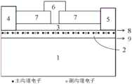
图2是本发明实施例提供的现有技术中氮化镓晶体管器件结构的示意图;FIG. 2 is a schematic diagram of a device structure of a gallium nitride transistor in the prior art provided by an embodiment of the present invention;
图3是本发明实施例提供的另一种同质外延氮化镓晶体管器件结构的示意图。FIG. 3 is a schematic diagram of another device structure of a homoepitaxial gallium nitride transistor according to an embodiment of the present invention.
具体实施方式Detailed ways
以下描述中,为了说明而不是为了限定,提出了诸如特定系统结构、技术之类的具体细节,以便透彻理解本发明实施例。然而,本领域的技术人员应当清楚,在没有这些具体细节的其它实施例中也可以实现本发明。在其它情况中,省略对众所周知的系统、装置、电路以及方法的详细说明,以免不必要的细节妨碍本发明的描述。In the following description, for the purpose of illustration rather than limitation, specific details such as specific system structures and technologies are set forth in order to provide a thorough understanding of the embodiments of the present invention. However, it will be apparent to those skilled in the art that the present invention may be practiced in other embodiments without these specific details. In other instances, detailed descriptions of well-known systems, devices, circuits, and methods are omitted so as not to obscure the description of the present invention with unnecessary detail.
本发明的说明书和权利要求书及上述附图中的术语“包括”以及它们任何变形,意图在于覆盖不排他的包含。例如包含一系列步骤或单元的过程、方法或系统、产品或设备没有限定于已列出的步骤或单元,而是可选地还包括没有列出的步骤或单元,或可选地还包括对于这些过程、方法、产品或设备固有的其它步骤或单元。此外,术语“第一”、“第二”和“第三”等是用于区别不同对象,而非用于描述特定顺序。The term "comprising" and any variations thereof in the description and claims of the present invention and the above drawings are intended to cover non-exclusive inclusions. For example, a process, method or system, product or device comprising a series of steps or units is not limited to the listed steps or units, but optionally also includes unlisted steps or units, or optionally also includes Other steps or units inherent in these processes, methods, products or devices. In addition, the terms "first", "second", "third", etc. are used to distinguish different objects and not to describe a particular order.
为了说明本发明所述的技术方案,下面通过具体实施例来进行说明。In order to illustrate the technical solutions of the present invention, the following specific embodiments are used for description.
实施例1:Example 1:
本发明的一个实施例提供了一种同质外延氮化镓晶体管器件结构,其结构如下所述:An embodiment of the present invention provides a device structure of a homoepitaxial gallium nitride transistor, the structure of which is as follows:
如图1所示,图1示出了本发明实施例提供的同质外延氮化镓晶体管器件的结构示意图,其包括:As shown in FIG. 1, FIG. 1 shows a schematic structural diagram of a homoepitaxial gallium nitride transistor device provided by an embodiment of the present invention, which includes:
衬底1、位于衬底1上的沟道层2、位于沟道层2上的势垒层3及位于势垒层3上的电极,所述电极包括源电极4、漏电极5和栅电极6;
所述源电极4和所述漏电极5分别位于所述势垒层3上表面的两侧,所述栅电极6位于所述源电极4和所述漏电极5之间的所述势垒层3上;The
所述沟道层厚度范围满足1nm≤d1≤20nm,所述势垒层厚度范围满足d2>12nm,所述d1表示所述沟道层厚度,所述d2表示所述势垒层厚度。The thickness range of the channel layer satisfies 1nm≤d1 ≤20nm, the thickness range of the barrier layer satisfies d2 >12nm, the d1 represents the thickness of the channel layer, and the d2 represents the barrier layer thickness.
在本实施例中,如图1所示,衬底1上设有沟道层2,沟道层2上设有势垒层3,势垒层3上表面的两侧设有源电极4和漏电极5,栅电极6设在源电极4和漏电极5之间,且同样位于所述势垒层3上。In this embodiment, as shown in FIG. 1 , a
现有技术中,如图2所示,图2示出了现有技术中氮化镓晶体管的结构示意图,图2中,沟道层2和势垒层3之间存在主沟道8,主沟道8存在主沟道8电子,沟道层2和衬底1间存在副沟道9,副沟道9内存在副沟道9电子,因此,器件漏电会很大。In the prior art, as shown in FIG. 2, FIG. 2 shows a schematic structural diagram of a gallium nitride transistor in the prior art. In FIG. 2, a
本实施例中,沟道层厚度设置为1nm~20nm之间,薄沟道层2能够使副沟道9电子进入主沟道8,从而增加主沟道8二维电子气浓度,有利于提高饱和电流。同时本实施例不引入新的工艺,不会造成新的缺陷,具有工艺简单、外延成本低外延时间降低的优势。In this embodiment, the thickness of the channel layer is set to be between 1 nm and 20 nm, and the
在本实施例中,沟道层2为超薄层,并且沟道层2未引入杂质补偿,不会造成电流崩塌增大和饱和电流降低的现象。In this embodiment, the
在一个实施例中,所述衬底1为在蓝宝石、碳化硅、硅或金刚石的基础上外延一层氮化镓的衬底1。In one embodiment, the
在一个实施例中,所述氮化镓衬底1为纯氮化镓衬底。In one embodiment, the
在一个实施例中,所述沟道层2为InmAlnGarN;其中,0≤m≤1,0≤n≤0.1,0.9≤r≤1且m+n+r=1。In one embodiment, the
在一个实施例中,所述沟道层2为InGaN。In one embodiment, the
在一个实施例中,所述势垒层3为InxAlyGazN;其中,0≤x≤0.85,0.15≤y≤1,0≤z≤0.85且x+y+z=1。In one embodiment, the
在一个实施例中,如图1所示,还包括钝化层7,所述钝化层7位于所述源电极4和所述栅电极6之间、以及所述栅电极6和所述漏电极5之间的所述势垒层3上。In one embodiment, as shown in FIG. 1, a
在一个实施例中,所述栅电极6为T型栅、直栅、Y型栅、TT栅和U型栅中的任意一种。In one embodiment, the
在一个实施例中,如图3所示,图3示出了另一种同质外延氮化镓晶体管器件结构的示意图。In one embodiment, as shown in FIG. 3 , FIG. 3 shows a schematic diagram of another device structure of a homoepitaxial gallium nitride transistor.
如图3所示,所述栅电极6为直栅,所述同质外延氮化镓晶体管器件结构还包括栅介质层10,所述栅介质层10位于所述直栅下方的势垒层3上。As shown in FIG. 3 , the
在一个实施例中,所述栅电极6为肖特基栅极。In one embodiment, the
本发明实施例提供的同质外延氮化镓晶体管器件结构包括:衬底1、位于衬底1上的沟道层2、位于沟道层2上的势垒层3及位于势垒层3上的电极,所述电极包括源电极4、漏电极5和栅电极6;所述源电极4和所述漏电极5分别位于所述势垒层3上表面的两侧,所述栅电极6位于所述源电极4和所述漏电极5之间的所述势垒层3上;所述沟道层厚度范围满足1nm≤d1≤20nm,所述势垒层厚度范围满足d2>12nm。本申请通过设置薄沟道层2,使得副沟道9的电子能够进入异质结界面主沟道8中,变为可控的主沟道8电子,从而降低泄露电流。The device structure of the homoepitaxial gallium nitride transistor provided by the embodiment of the present invention includes: a
作为本发明的一个实施例,本实施例提供了一种具体的同质外延氮化镓晶体管器件结构,其包括:As an embodiment of the present invention, this embodiment provides a specific device structure of a homoepitaxial gallium nitride transistor, which includes:
衬底1、位于衬底1上的沟道层2、位于沟道层2上的势垒层3及位于势垒层3上的电极,所述电极包括源电极4、漏电极5和栅电极6;所述源电极4和所述漏电极5分别位于所述势垒层3上表面的两侧,所述栅电极6位于所述源电极4和所述漏电极5之间的所述势垒层3上;所述沟道层厚度范围满足1nm≤d1≤20nm,所述势垒层厚度范围满足d2>12nm,所述d1表示所述沟道层厚度,所述d2表示所述势垒层厚度。
具体的,沟道层2可以为GaN。Specifically, the
具体的,势垒层3为AlyGazN;其中,0.15≤y≤1,0≤z≤0.85且y+z=1。Specifically, the
具体的,栅电极6为T形栅。Specifically, the
作为本发明的又一实施例,本实施例还提供了一种具体的同质外延氮化镓晶体管器件结构,其包括:As another embodiment of the present invention, this embodiment also provides a specific device structure of a homoepitaxial gallium nitride transistor, which includes:
衬底1、位于衬底1上的沟道层2、位于沟道层2上的势垒层3及位于势垒层3上的电极,所述电极包括源电极4、漏电极5和栅电极6;所述源电极4和所述漏电极5分别位于所述势垒层3上表面的两侧,所述栅电极6位于所述源电极4和所述漏电极5之间的所述势垒层3上;所述沟道层厚度范围满足1nm≤d1≤20nm,所述势垒层厚度范围满足d2>12nm,所述d1表示所述沟道层厚度,所述d2表示所述势垒层厚度。
具体地,所述沟道层2未引入杂志补偿。Specifically, the
具体地,所述沟道层2为InGaN。Specifically, the
具体地,所示势垒层3为InxAlyN,其中,0≤x≤1,0≤y≤1,且x+y=1。Specifically, the illustrated
具体地,所述栅电极6为直栅,且在直栅下方,在势垒层3的上表面设有介质层。Specifically, the
具体地,所述栅为介质栅。Specifically, the gate is a dielectric gate.
本发明不限于上述实施方式,保护的是一种基于横向剪裁理论的III族氮化物材料新型增强型HEMT结构;根据上述实施例的描述,本领域的普通技术人员还可做出一些显而易见的改变,例如沟道层2材料选用多层复合材料、背势垒结构、多层缓冲层等结构,衬底1选用SiC、Si、金刚石、蓝宝石、GaN多层复合衬底,但这些改变均应落入本发明权利要求的保护范围之内。The present invention is not limited to the above-mentioned embodiments, and what is protected is a novel enhanced HEMT structure of group III nitride materials based on the lateral tailoring theory; according to the description of the above-mentioned embodiments, those of ordinary skill in the art can also make some obvious changes. For example, the
以上所述实施例仅用以说明本发明的技术方案,而非对其限制;尽管参照前述实施例对本发明进行了详细的说明,本领域的普通技术人员应当理解:其依然可以对前述各实施例所记载的技术方案进行修改,或者对其中部分技术特征进行等同替换;而这些修改或者替换,并不使相应技术方案的本质脱离本发明各实施例技术方案的精神和范围,均应包含在本发明的保护范围之内。The above-mentioned embodiments are only used to illustrate the technical solutions of the present invention, but not to limit them; although the present invention has been described in detail with reference to the foregoing embodiments, those of ordinary skill in the art should understand that: it is still possible to implement the foregoing implementations. The technical solutions described in the examples are modified, or some technical features thereof are equivalently replaced; and these modifications or replacements do not make the essence of the corresponding technical solutions deviate from the spirit and scope of the technical solutions of the embodiments of the present invention, and should be included in the within the protection scope of the present invention.
Claims (10)
Priority Applications (1)
| Application Number | Priority Date | Filing Date | Title |
|---|---|---|---|
| CN201910906108.XACN110690283A (en) | 2019-09-24 | 2019-09-24 | Homoepitaxial gallium nitride transistor device structure |
Applications Claiming Priority (1)
| Application Number | Priority Date | Filing Date | Title |
|---|---|---|---|
| CN201910906108.XACN110690283A (en) | 2019-09-24 | 2019-09-24 | Homoepitaxial gallium nitride transistor device structure |
Publications (1)
| Publication Number | Publication Date |
|---|---|
| CN110690283Atrue CN110690283A (en) | 2020-01-14 |
Family
ID=69110381
Family Applications (1)
| Application Number | Title | Priority Date | Filing Date |
|---|---|---|---|
| CN201910906108.XAPendingCN110690283A (en) | 2019-09-24 | 2019-09-24 | Homoepitaxial gallium nitride transistor device structure |
Country Status (1)
| Country | Link |
|---|---|
| CN (1) | CN110690283A (en) |
Citations (14)
| Publication number | Priority date | Publication date | Assignee | Title |
|---|---|---|---|---|
| US20040124435A1 (en)* | 2002-12-27 | 2004-07-01 | General Electric Company | Homoepitaxial gallium-nitride-based electronic devices and method for producing same |
| WO2004061923A1 (en)* | 2002-12-27 | 2004-07-22 | General Electric Company | Gallium nitride crystal, homoepitaxial gallium-nitride-based devices and method for producing same |
| CN1748290A (en)* | 2002-12-27 | 2006-03-15 | 通用电气公司 | Gallium nitride crystal, homoepitaxial gallium nitride-based device and manufacturing method thereof |
| CN102789982A (en)* | 2011-05-16 | 2012-11-21 | 中国科学院微电子研究所 | Enhanced AlN/GaN high electron mobility transistor and manufacturing method thereof |
| CN103594508A (en)* | 2013-11-26 | 2014-02-19 | 电子科技大学 | Gallium nitride high electron mobility transistor of grid single field plate |
| CN103681830A (en)* | 2012-09-11 | 2014-03-26 | 中国科学院微电子研究所 | Double-channel transistor and preparation method thereof |
| CN104167445A (en)* | 2014-08-29 | 2014-11-26 | 电子科技大学 | GaN-based enhancement/depletion mode heterojunction field effect transistor with buried gate structure |
| CN105355555A (en)* | 2015-10-28 | 2016-02-24 | 中国科学院微电子研究所 | GaN-based enhanced power electronic device and preparation method thereof |
| CN105914232A (en)* | 2016-05-06 | 2016-08-31 | 西安电子科技大学 | T-gate and N-surface GaN/AlGaN fin-type high electron mobility transistor |
| WO2017113484A1 (en)* | 2015-12-31 | 2017-07-06 | 深圳市华讯方舟微电子科技有限公司 | High electron mobility transistor and method for manufacturing same |
| CN108110054A (en)* | 2017-12-22 | 2018-06-01 | 苏州闻颂智能科技有限公司 | A kind of GaN base HEMT device and preparation method thereof |
| CN108598149A (en)* | 2018-04-20 | 2018-09-28 | 苏州闻颂智能科技有限公司 | A kind of GaN base HEMT device |
| CN109273527A (en)* | 2018-11-21 | 2019-01-25 | 芜湖启迪半导体有限公司 | Semiconductor structure and method of forming same |
| CN109659363A (en)* | 2018-11-20 | 2019-04-19 | 西安电子科技大学芜湖研究院 | A kind of preparation method of the low ohm contact structures of gallium nitride HEMT structure |
- 2019
- 2019-09-24CNCN201910906108.XApatent/CN110690283A/enactivePending
Patent Citations (14)
| Publication number | Priority date | Publication date | Assignee | Title |
|---|---|---|---|---|
| US20040124435A1 (en)* | 2002-12-27 | 2004-07-01 | General Electric Company | Homoepitaxial gallium-nitride-based electronic devices and method for producing same |
| WO2004061923A1 (en)* | 2002-12-27 | 2004-07-22 | General Electric Company | Gallium nitride crystal, homoepitaxial gallium-nitride-based devices and method for producing same |
| CN1748290A (en)* | 2002-12-27 | 2006-03-15 | 通用电气公司 | Gallium nitride crystal, homoepitaxial gallium nitride-based device and manufacturing method thereof |
| CN102789982A (en)* | 2011-05-16 | 2012-11-21 | 中国科学院微电子研究所 | Enhanced AlN/GaN high electron mobility transistor and manufacturing method thereof |
| CN103681830A (en)* | 2012-09-11 | 2014-03-26 | 中国科学院微电子研究所 | Double-channel transistor and preparation method thereof |
| CN103594508A (en)* | 2013-11-26 | 2014-02-19 | 电子科技大学 | Gallium nitride high electron mobility transistor of grid single field plate |
| CN104167445A (en)* | 2014-08-29 | 2014-11-26 | 电子科技大学 | GaN-based enhancement/depletion mode heterojunction field effect transistor with buried gate structure |
| CN105355555A (en)* | 2015-10-28 | 2016-02-24 | 中国科学院微电子研究所 | GaN-based enhanced power electronic device and preparation method thereof |
| WO2017113484A1 (en)* | 2015-12-31 | 2017-07-06 | 深圳市华讯方舟微电子科技有限公司 | High electron mobility transistor and method for manufacturing same |
| CN105914232A (en)* | 2016-05-06 | 2016-08-31 | 西安电子科技大学 | T-gate and N-surface GaN/AlGaN fin-type high electron mobility transistor |
| CN108110054A (en)* | 2017-12-22 | 2018-06-01 | 苏州闻颂智能科技有限公司 | A kind of GaN base HEMT device and preparation method thereof |
| CN108598149A (en)* | 2018-04-20 | 2018-09-28 | 苏州闻颂智能科技有限公司 | A kind of GaN base HEMT device |
| CN109659363A (en)* | 2018-11-20 | 2019-04-19 | 西安电子科技大学芜湖研究院 | A kind of preparation method of the low ohm contact structures of gallium nitride HEMT structure |
| CN109273527A (en)* | 2018-11-21 | 2019-01-25 | 芜湖启迪半导体有限公司 | Semiconductor structure and method of forming same |
Similar Documents
| Publication | Publication Date | Title |
|---|---|---|
| CN1599960B (en) | Strain balanced nitride heterojunction transistors and methods of fabricating strain balanced nitride heterojunction transistors | |
| US9620362B2 (en) | Seed layer structure for growth of III-V materials on silicon | |
| US20090045439A1 (en) | Heterojunction field effect transistor and manufacturing method thereof | |
| US9385199B2 (en) | Normally-off gallium nitride-based semiconductor devices | |
| US20090001384A1 (en) | Group III Nitride semiconductor HFET and method for producing the same | |
| US20210057561A1 (en) | High electron mobility transistor device and methods for forming the same | |
| US11114555B2 (en) | High electron mobility transistor device and methods for forming the same | |
| JP2002076023A (en) | Semiconductor device | |
| JP2002076329A (en) | Semiconductor device | |
| CN102365747A (en) | Compensated gate MISFET and its manufacturing method | |
| US20150001582A1 (en) | HEMT Structure with Iron-Doping-Stop Component and Methods of Forming | |
| US9847223B2 (en) | Buffer stack for group IIIA-N devices | |
| US9653591B2 (en) | Compound semiconductor device having at least one buried semiconductor material region | |
| EP2869347A1 (en) | Group III-V device including a buffer termination body | |
| US10529561B2 (en) | Method of fabricating non-etch gas cooled epitaxial stack for group IIIA-N devices | |
| WO2022016390A1 (en) | Semiconductor structure | |
| KR20150091703A (en) | Nitride semiconductor and method thereof | |
| CN104409492A (en) | Nitrogen polar GaN transistor | |
| US11610989B2 (en) | High electron mobility transistor | |
| TW202523101A (en) | High electron mobility transistor | |
| CN110690283A (en) | Homoepitaxial gallium nitride transistor device structure | |
| CN106206709A (en) | Semiconductor device | |
| JP2011258782A (en) | Nitride semiconductor substrate | |
| US12349377B2 (en) | Preparation method for semiconductor structure involving the replacement of dielectric layer with gate | |
| TWI748225B (en) | Enhancement mode hemt device |
Legal Events
| Date | Code | Title | Description |
|---|---|---|---|
| PB01 | Publication | ||
| PB01 | Publication | ||
| SE01 | Entry into force of request for substantive examination | ||
| SE01 | Entry into force of request for substantive examination | ||
| RJ01 | Rejection of invention patent application after publication | Application publication date:20200114 | |
| RJ01 | Rejection of invention patent application after publication |