CN110690227A - Array substrate, manufacturing method thereof, and display device - Google Patents
Array substrate, manufacturing method thereof, and display deviceDownload PDFInfo
- Publication number
- CN110690227A CN110690227ACN201910834990.1ACN201910834990ACN110690227ACN 110690227 ACN110690227 ACN 110690227ACN 201910834990 ACN201910834990 ACN 201910834990ACN 110690227 ACN110690227 ACN 110690227A
- Authority
- CN
- China
- Prior art keywords
- thin film
- film transistor
- transistor device
- layer
- array substrate
- Prior art date
- Legal status (The legal status is an assumption and is not a legal conclusion. Google has not performed a legal analysis and makes no representation as to the accuracy of the status listed.)
- Pending
Links
- 239000000758substrateSubstances0.000titleclaimsabstractdescription51
- 238000004519manufacturing processMethods0.000titleclaimsabstractdescription10
- 239000010409thin filmSubstances0.000claimsabstractdescription77
- 239000000463materialSubstances0.000claimsabstractdescription49
- 239000003990capacitorSubstances0.000claimsdescription26
- 238000000034methodMethods0.000claimsdescription17
- 229910052751metalInorganic materials0.000claimsdescription12
- 239000002184metalSubstances0.000claimsdescription12
- XLOMVQKBTHCTTD-UHFFFAOYSA-NZinc monoxideChemical compound[Zn]=OXLOMVQKBTHCTTD-UHFFFAOYSA-N0.000claimsdescription10
- 229910021420polycrystalline siliconInorganic materials0.000claimsdescription10
- 229920005591polysiliconPolymers0.000claimsdescription10
- 239000004065semiconductorSubstances0.000claimsdescription6
- 229910021417amorphous siliconInorganic materials0.000claimsdescription5
- 230000005525hole transportEffects0.000claimsdescription5
- 239000011787zinc oxideSubstances0.000claimsdescription5
- GYHNNYVSQQEPJS-UHFFFAOYSA-NGalliumChemical compound[Ga]GYHNNYVSQQEPJS-UHFFFAOYSA-N0.000claimsdescription4
- 229910052733galliumInorganic materials0.000claimsdescription4
- 229910052738indiumInorganic materials0.000claimsdescription4
- APFVFJFRJDLVQX-UHFFFAOYSA-Nindium atomChemical compound[In]APFVFJFRJDLVQX-UHFFFAOYSA-N0.000claimsdescription4
- 239000002210silicon-based materialSubstances0.000claimsdescription4
- 230000035945sensitivityEffects0.000abstractdescription10
- 230000000694effectsEffects0.000abstractdescription5
- 239000010410layerSubstances0.000description89
- 239000011229interlayerSubstances0.000description9
- 238000010586diagramMethods0.000description5
- 229910052750molybdenumInorganic materials0.000description4
- 230000003287optical effectEffects0.000description4
- 125000006850spacer groupChemical group0.000description3
- 229910052782aluminiumInorganic materials0.000description2
- 239000010949copperSubstances0.000description2
- 239000010408filmSubstances0.000description2
- 239000004973liquid crystal related substanceSubstances0.000description2
- 229910052719titaniumInorganic materials0.000description2
- 239000010936titaniumSubstances0.000description2
- RYGMFSIKBFXOCR-UHFFFAOYSA-NCopperChemical compound[Cu]RYGMFSIKBFXOCR-UHFFFAOYSA-N0.000description1
- 229910015711MoOxInorganic materials0.000description1
- ZOKXTWBITQBERF-UHFFFAOYSA-NMolybdenumChemical compound[Mo]ZOKXTWBITQBERF-UHFFFAOYSA-N0.000description1
- 229910052581Si3N4Inorganic materials0.000description1
- RTAQQCXQSZGOHL-UHFFFAOYSA-NTitaniumChemical compound[Ti]RTAQQCXQSZGOHL-UHFFFAOYSA-N0.000description1
- XAGFODPZIPBFFR-UHFFFAOYSA-NaluminiumChemical compound[Al]XAGFODPZIPBFFR-UHFFFAOYSA-N0.000description1
- 230000009286beneficial effectEffects0.000description1
- 229910052802copperInorganic materials0.000description1
- 238000005530etchingMethods0.000description1
- AMGQUBHHOARCQH-UHFFFAOYSA-Nindium;oxotinChemical compound[In].[Sn]=OAMGQUBHHOARCQH-UHFFFAOYSA-N0.000description1
- 230000009191jumpingEffects0.000description1
- 239000011733molybdenumSubstances0.000description1
- HQVNEWCFYHHQES-UHFFFAOYSA-Nsilicon nitrideChemical compoundN12[Si]34N5[Si]62N3[Si]51N64HQVNEWCFYHHQES-UHFFFAOYSA-N0.000description1
Images


Classifications
- H—ELECTRICITY
- H10—SEMICONDUCTOR DEVICES; ELECTRIC SOLID-STATE DEVICES NOT OTHERWISE PROVIDED FOR
- H10D—INORGANIC ELECTRIC SEMICONDUCTOR DEVICES
- H10D86/00—Integrated devices formed in or on insulating or conducting substrates, e.g. formed in silicon-on-insulator [SOI] substrates or on stainless steel or glass substrates
- H10D86/40—Integrated devices formed in or on insulating or conducting substrates, e.g. formed in silicon-on-insulator [SOI] substrates or on stainless steel or glass substrates characterised by multiple TFTs
- H—ELECTRICITY
- H10—SEMICONDUCTOR DEVICES; ELECTRIC SOLID-STATE DEVICES NOT OTHERWISE PROVIDED FOR
- H10D—INORGANIC ELECTRIC SEMICONDUCTOR DEVICES
- H10D86/00—Integrated devices formed in or on insulating or conducting substrates, e.g. formed in silicon-on-insulator [SOI] substrates or on stainless steel or glass substrates
- H10D86/01—Manufacture or treatment
- H10D86/021—Manufacture or treatment of multiple TFTs
- H—ELECTRICITY
- H10—SEMICONDUCTOR DEVICES; ELECTRIC SOLID-STATE DEVICES NOT OTHERWISE PROVIDED FOR
- H10D—INORGANIC ELECTRIC SEMICONDUCTOR DEVICES
- H10D86/00—Integrated devices formed in or on insulating or conducting substrates, e.g. formed in silicon-on-insulator [SOI] substrates or on stainless steel or glass substrates
- H10D86/40—Integrated devices formed in or on insulating or conducting substrates, e.g. formed in silicon-on-insulator [SOI] substrates or on stainless steel or glass substrates characterised by multiple TFTs
- H10D86/471—Integrated devices formed in or on insulating or conducting substrates, e.g. formed in silicon-on-insulator [SOI] substrates or on stainless steel or glass substrates characterised by multiple TFTs having different architectures, e.g. having both top-gate and bottom-gate TFTs
- H—ELECTRICITY
- H10—SEMICONDUCTOR DEVICES; ELECTRIC SOLID-STATE DEVICES NOT OTHERWISE PROVIDED FOR
- H10D—INORGANIC ELECTRIC SEMICONDUCTOR DEVICES
- H10D86/00—Integrated devices formed in or on insulating or conducting substrates, e.g. formed in silicon-on-insulator [SOI] substrates or on stainless steel or glass substrates
- H10D86/40—Integrated devices formed in or on insulating or conducting substrates, e.g. formed in silicon-on-insulator [SOI] substrates or on stainless steel or glass substrates characterised by multiple TFTs
- H10D86/60—Integrated devices formed in or on insulating or conducting substrates, e.g. formed in silicon-on-insulator [SOI] substrates or on stainless steel or glass substrates characterised by multiple TFTs wherein the TFTs are in active matrices
- H—ELECTRICITY
- H10—SEMICONDUCTOR DEVICES; ELECTRIC SOLID-STATE DEVICES NOT OTHERWISE PROVIDED FOR
- H10K—ORGANIC ELECTRIC SOLID-STATE DEVICES
- H10K59/00—Integrated devices, or assemblies of multiple devices, comprising at least one organic light-emitting element covered by group H10K50/00
- H10K59/40—OLEDs integrated with touch screens
Landscapes
- Solid State Image Pick-Up Elements (AREA)
- Liquid Crystal (AREA)
- Devices For Indicating Variable Information By Combining Individual Elements (AREA)
Abstract
Translated fromChinese
Description
Translated fromChinese技术领域technical field
本发明涉及显示技术领域,尤其涉及一种阵列基板及其制作方法、显示装置。The present invention relates to the field of display technology, and in particular, to an array substrate, a manufacturing method thereof, and a display device.
背景技术Background technique
指纹识别技术已经广泛应用于平板、手机等中小尺寸面板中。光学指纹识别技术采用光的反射原理,当手指放在感光传感器上方时,指纹的谷和脊对光的反射不一样,感光传感器所接收到的反射光强就不一样,产生不同大小的光电流,从而抓取指纹的特征点进行识别。Fingerprint recognition technology has been widely used in small and medium-sized panels such as tablets and mobile phones. Optical fingerprint recognition technology uses the principle of light reflection. When the finger is placed on the photosensitive sensor, the valleys and ridges of the fingerprint reflect light differently, and the reflected light intensity received by the photosensitive sensor is different, resulting in different sizes of photocurrents. , so as to capture the feature points of the fingerprint for identification.
目前,市场上的手机使用的光学指纹识别功能大多是集成在OLED屏幕下方,通过小孔方式实现。而对于中小尺寸的LCD屏幕,由于其显示原理与自发光的OLED不同,要将光学指纹的感光传感器集成到LCD的屏内,需要牺牲一定的开口率,并且感光传感器所接触到的手指反射光的强度也相对OLED要小很多,因此加大了LCD的屏内指纹识别的设计难度。At present, most of the optical fingerprint recognition functions used in mobile phones on the market are integrated under the OLED screen and implemented through small holes. For small and medium-sized LCD screens, since the display principle is different from that of self-luminous OLEDs, to integrate the photosensitive sensor of optical fingerprints into the LCD screen, a certain aperture ratio needs to be sacrificed, and the finger that the photosensitive sensor touches reflects light. The strength of the LCD is also much smaller than that of the OLED, which increases the difficulty of designing the fingerprint recognition in the LCD screen.
目前主流的中小尺寸液晶显示屏幕是采用低温多晶硅(LTPS)工艺制成,但是由于多晶硅的漏电流(Ioff~10-13A)相对氧化物半导体IGZO(Ioff~10-15A)要高很多,而感光传感器所能够产生的光生电流是很微弱的,如果使用多晶硅作为指纹传感器的驱动TFT,则会大大降低传感器的灵敏度。At present, the mainstream small and medium-sized liquid crystal display screen is made of low temperature polysilicon (LTPS) process, but because the leakage current of polysilicon (Ioff ~ 10-13A) is much higher than that of oxide semiconductor IGZO (Ioff ~ 10-15A), and the photosensitive The photo-generated current generated by the sensor is very weak. If polysilicon is used as the driving TFT of the fingerprint sensor, the sensitivity of the sensor will be greatly reduced.
发明内容SUMMARY OF THE INVENTION
本发明提供一种阵列基板及其制作方法、显示装置,能够减小感光驱动薄膜电晶体器件的漏电流,从而解决了现有技术中感光驱动薄膜电晶体器件的漏电流较大,导致感光传感器的灵敏度降低,进而影响显示的技术问题。The present invention provides an array substrate, a manufacturing method thereof, and a display device, which can reduce the leakage current of the photosensitive driving thin film transistor device, thereby solving the problem that the leakage current of the photosensitive driving thin film transistor device in the prior art is relatively large, causing the photosensitive sensor The sensitivity of the display is reduced, which in turn affects the technical problems of the display.
为解决上述问题,本发明提供的技术方案如下:For solving the above problems, the technical solutions provided by the present invention are as follows:
本发明提供一种阵列基板,包括:The present invention provides an array substrate, comprising:
显示区,所述显示区包括指纹识别区以及非指纹识别区;a display area, the display area includes a fingerprint identification area and a non-fingerprint identification area;
第一薄膜电晶体器件,设置于所述指纹识别区内,且所述第一薄膜电晶体器件的有源层的材质包括低漏电流材料,其中所述低漏电流材料的漏电流介于10-14A至10-15A;The first thin film transistor device is arranged in the fingerprint identification area, and the material of the active layer of the first thin film transistor device includes a low leakage current material, wherein the leakage current of the low leakage current material is between 10-14 A to 10-15 A;
第二薄膜电晶体器件,设置于所述非指纹识别区内,且所述第二薄膜电晶体器件的有源层的材质包括高迁移率材料,其中所述高迁移率材料的迁移率介于100至200厘米2/(伏·秒)。The second thin film transistor device is disposed in the non-fingerprint identification area, and the material of the active layer of the second thin film transistor device includes a high mobility material, wherein the mobility of the high mobility material is between 100 to 200 cm2 /(V·sec).
根据本发明一优选实施例,所述第一薄膜电晶体器件的栅极与所述第二薄膜电晶体器件的源漏极位于所述阵列基板的同一层。According to a preferred embodiment of the present invention, the gate electrode of the first thin film transistor device and the source and drain electrodes of the second thin film transistor device are located on the same layer of the array substrate.
根据本发明一优选实施例,所述低漏电流材料包括铟镓锌氧化物或非晶硅材料。According to a preferred embodiment of the present invention, the low leakage current material includes indium gallium zinc oxide or amorphous silicon material.
根据本发明一优选实施例,所述高迁移率材料包括多晶硅材料。According to a preferred embodiment of the present invention, the high mobility material includes polysilicon material.
根据本发明一优选实施例,所述阵列基板还包括感光传感器,所述感光传感器设置于所述指纹识别区内,且所述感光传感器包括依次层叠设置的第一电极层、电子传输层、半导体层、空穴传输层以及第二电极层,且所述第一电极层由所述第一薄膜电晶体器件的漏极所构成。According to a preferred embodiment of the present invention, the array substrate further includes a photosensitive sensor, the photosensitive sensor is disposed in the fingerprint identification area, and the photosensitive sensor includes a first electrode layer, an electron transport layer, and a semiconductor layer that are stacked in sequence. layer, a hole transport layer and a second electrode layer, and the first electrode layer is composed of the drain electrode of the first thin film transistor device.
根据本发明一优选实施例,所述阵列基板还包括存储电容,且所述存储电容设置于所述指纹识别区内,所述存储电容包括上电极以及下电极;According to a preferred embodiment of the present invention, the array substrate further includes a storage capacitor, and the storage capacitor is disposed in the fingerprint identification area, and the storage capacitor includes an upper electrode and a lower electrode;
其中,所述上电极由所述第一薄膜电晶体器件的漏极所构成,且所述下电极与所述第一薄膜电晶体器件的栅极位于所述阵列基板的同一层。Wherein, the upper electrode is formed by the drain electrode of the first thin film transistor device, and the lower electrode and the gate electrode of the first thin film transistor device are located on the same layer of the array substrate.
根据本发明一优选实施例,所述第二电极层通过过孔与所述下电极电连接。According to a preferred embodiment of the present invention, the second electrode layer is electrically connected to the lower electrode through a via hole.
一种阵列基板的制作方法,所述方法包括如下步骤:A method of fabricating an array substrate, the method comprising the following steps:
S10、提供基板;S10. Provide a substrate;
S20、形成第一金属层在所述基板上,其中所述第一金属层包括第一薄膜电晶体器件的栅极、第二薄膜电晶体器件的源漏极、以及存储电容的下电极;S20, forming a first metal layer on the substrate, wherein the first metal layer includes the gate of the first thin film transistor device, the source and drain of the second thin film transistor device, and the lower electrode of the storage capacitor;
S30、在所述第一金属层上依次制备沟道保护层、平坦层、绝缘层以及电极层;S30, sequentially preparing a channel protection layer, a flat layer, an insulating layer and an electrode layer on the first metal layer;
S40、蚀刻所述沟道保护层、所述平坦层、以及所述绝缘层,以形成第一过孔以及第二过孔,其中所述第一过孔暴露所述第一薄膜电晶体器件的漏极,所述第二过孔暴露所述存储电容的下电极;以及S40. Etch the channel protection layer, the flat layer, and the insulating layer to form a first via hole and a second via hole, wherein the first via hole exposes the first via hole of the first thin film transistor device. a drain, the second via exposes a lower electrode of the storage capacitor; and
S50、在所述第一过孔中制备感光传感器,其中所述感光传感器通过所述第一过孔与所述第一薄膜电晶体器件的漏极电连接,以及所述感光传感器通过所述第二过孔与所述存储电容的下电极电连接。S50. Prepare a photosensitive sensor in the first via hole, wherein the photosensitive sensor is electrically connected to the drain of the first thin film transistor device through the first via hole, and the photosensitive sensor passes through the first via hole. The two via holes are electrically connected to the lower electrode of the storage capacitor.
根据本发明一优选实施例,所述下电极与所述第一薄膜电晶体器件的漏极构成存储电容,以存储光生电流的电荷量。According to a preferred embodiment of the present invention, the lower electrode and the drain electrode of the first thin film transistor form a storage capacitor to store the electric charge of the photo-generated current.
一种显示装置,所述显示装置包括所述阵列基板。A display device comprising the array substrate.
本发明的有益效果为:本发明通过在指纹识别区设置低漏电流的薄膜电晶体器件,在非指纹识别区设置高迁移率的薄膜电晶体器件,在提高显示效果的同时,还提高了指纹识别的灵敏度,并将指纹识别集成于屏幕下方,提高了屏占比。The beneficial effects of the present invention are as follows: the present invention provides a thin film transistor device with low leakage current in the fingerprint identification area and a thin film transistor device with high mobility in the non-fingerprint identification area, which not only improves the display effect, but also improves the fingerprint identification The sensitivity of the recognition, and the fingerprint recognition is integrated at the bottom of the screen, which improves the screen ratio.
附图说明Description of drawings
为了更清楚地说明实施例或现有技术中的技术方案,下面将对实施例或现有技术描述中所需要使用的附图作简单介绍,显而易见地,下面描述中的附图仅仅是发明的一些实施例,对于本领域普通技术人员来讲,在不付出创造性劳动的前提下,还可以根据这些附图获得其他的附图。In order to more clearly illustrate the embodiments or technical solutions in the prior art, the following briefly introduces the accompanying drawings that are used in the description of the embodiments or the prior art. Obviously, the drawings in the following description are only for invention. In some embodiments, for those of ordinary skill in the art, other drawings can also be obtained according to these drawings without any creative effort.
图1为本发明实施例提供的阵列基板结构示意图。FIG. 1 is a schematic structural diagram of an array substrate according to an embodiment of the present invention.
图2为本发明实施例提供的阵列基板的制作方法流程图。FIG. 2 is a flowchart of a method for fabricating an array substrate according to an embodiment of the present invention.
图3为本发明实施例提供的阵列基板的制作方法过程示意图。FIG. 3 is a schematic process diagram of a method for fabricating an array substrate according to an embodiment of the present invention.
图4为本发明实施例提供的阵列基板的制作方法过程示意图。FIG. 4 is a schematic process diagram of a method for fabricating an array substrate according to an embodiment of the present invention.
图5为本发明实施例提供的阵列基板的制作方法过程示意图。FIG. 5 is a schematic process diagram of a manufacturing method of an array substrate according to an embodiment of the present invention.
具体实施方式Detailed ways
以下各实施例的说明是参考附加的图示,用以例示本发明可用以实施的特定实施例。本发明所提到的方向用语,例如[上]、[下]、[前]、[后]、[左]、[右]、[内]、[外]、[侧面]等,仅是参考附加图式的方向。因此,使用的方向用语是用以说明及理解本发明,而非用以限制本发明。在图中,结构相似的单元是用以相同标号表示。The following descriptions of the various embodiments refer to the accompanying drawings to illustrate specific embodiments in which the invention may be practiced. The directional terms mentioned in the present invention, such as [up], [down], [front], [rear], [left], [right], [inner], [outer], [side], etc., are only for reference Additional schema orientation. Therefore, the directional terms used are for describing and understanding the present invention, not for limiting the present invention. In the figures, structurally similar elements are denoted by the same reference numerals.
本发明针对现有的阵列基板及其制作方法、显示装置,由于在光学指纹识别中,感光传感器产生的光生电流很微弱,而一般TFT器件的漏电流较大,使得感光传感器的灵敏度降低,进而影响显示的技术问题,本实施例能够解决该缺陷。The present invention is aimed at the existing array substrate and its manufacturing method and display device, because in the optical fingerprint identification, the photo-generated current generated by the photosensitive sensor is very weak, while the leakage current of the general TFT device is relatively large, so that the sensitivity of the photosensitive sensor is reduced, and further The technical problem affecting the display can be solved by this embodiment.
本实施例提供一种阵列基板,包括:This embodiment provides an array substrate, including:
显示区,所述显示区包括指纹识别区以及非指纹识别区;a display area, the display area includes a fingerprint identification area and a non-fingerprint identification area;
第一薄膜电晶体器件,设置于所述指纹识别区内,且所述第一薄膜电晶体器件的有源层的材质包括低漏电流材料,其中所述低漏电流材料的漏电流介于10-14A至10-15A;The first thin film transistor device is arranged in the fingerprint identification area, and the material of the active layer of the first thin film transistor device includes a low leakage current material, wherein the leakage current of the low leakage current material is between 10-14 A to 10-15 A;
第二薄膜电晶体器件,设置于所述非指纹识别区内,且所述第二薄膜电晶体器件的有源层的材质包括高迁移率材料,其中所述高迁移率材料的迁移率介于100至200厘米2/(伏·秒)。The second thin film transistor device is disposed in the non-fingerprint identification area, and the material of the active layer of the second thin film transistor device includes a high mobility material, wherein the mobility of the high mobility material is between 100 to 200 cm2 /(V·sec).
本实施例通过在指纹识别区设置低漏电流性质的第一薄膜电晶体器件101,在非指纹识别区设置高迁移率性质的第二薄膜电晶体器件102,以此既可以保证显示装置的显示效果,又提高了指纹识别的灵敏度。In this embodiment, the first thin
在实施应用过程中,由于中小尺寸液晶显示屏幕是采用低温多晶硅工艺制成,但是由于多晶硅的漏电流较大,而感光传感器所能够产生的光生电流是很微弱的,如果使用多晶硅作为指纹传感器的驱动薄膜电晶体器件,则会大大降低传感器的灵敏度,因此,本发明实施例中通过在指纹识别区设置具有低漏电流性质的第一薄膜电晶体器件,在非指纹识别区设置具有高迁移率性质的第二薄膜电晶体器件,以此既可以保证显示装置的显示效果,又提高了指纹识别的灵敏度。During the application process, the small and medium-sized liquid crystal display screen is made of low-temperature polysilicon technology, but due to the large leakage current of polysilicon, the photo-generated current generated by the photosensitive sensor is very weak. If polysilicon is used as the fingerprint sensor Driving the thin film transistor device will greatly reduce the sensitivity of the sensor. Therefore, in the embodiment of the present invention, the first thin film transistor device with low leakage current is disposed in the fingerprint identification area, and the high mobility is disposed in the non-fingerprint identification area. The second thin film transistor device of the nature can not only ensure the display effect of the display device, but also improve the sensitivity of fingerprint identification.
进一步地,所述低漏电流材料包括铟镓锌氧化物或非晶硅材料,所述高迁移率材料包括多晶硅材料。Further, the low leakage current material includes indium gallium zinc oxide or amorphous silicon material, and the high mobility material includes polysilicon material.
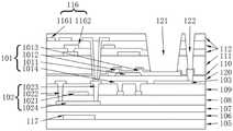
具体地,如图1所示,为本实施例提供的阵列基板的结构示意图,其中,所述阵列基板包括基板105,设置于所述基板105上的第一薄膜电晶体器件101、第二薄膜电晶体器件102、感光传感器118,存储电容119以及多个绝缘层和功能膜层。Specifically, as shown in FIG. 1 , which is a schematic structural diagram of an array substrate provided in this embodiment, the array substrate includes a
在本实施例中,所述第一薄膜电晶体器件101为底栅结构,设置于所述指纹识别区内,且所述第一薄膜电晶体器件101包括栅极1014、有源层1011、源极1012以及漏极1013。In this embodiment, the first thin
所述第二薄膜电晶体器件102为顶栅结构,设置于所述非指纹识别区内,且所述第二薄膜电晶体器件102包括栅极1021、有源层1024、源极1022以及漏极1023。The second thin
所述感光传感器118设置于所述第一薄膜电晶体器件101的漏极1013上,位于所述指纹识别区内,包括依次层叠设置的第一电极层、电子传输层113、半导体层114、空穴传输层115以及第二电极层104,其中,所述第一电极层由所述第一薄膜电晶体器件101的漏极1013所构成。The
所述存储电容119设置于所述指纹识别区内,且所述存储电容包括上电极以及下电极103,其中,所述上电极由所述第一薄膜电晶体器件101的漏极1013所构成,所述下电极103与所述第一薄膜电晶体器件101的栅极1014位于所述阵列基板的同一层。The
且所述第二电极层104通过过孔与所述存储电容的下电极103电连接。And the
另外,在本实施例中,所述第一薄膜电晶体器件101的栅极1014与所述第二薄膜电晶体器件102的源漏极1022和1023位于所述阵列基板的同一层,且所述第一薄膜电晶体器件101的栅极1014可采用跳线的方式制备,节省了一道光罩的制作工序。In addition, in this embodiment, the
综上,在本实施例中,所述感光传感器118为一个光敏二极管,当其接收到手指反射的光后,将产生光生电流,并给所述存储电容119进行充电,接着打开所述第一薄膜电晶体器件101,读取并识别存储的电荷信号,以进行指纹识别过程,而本实施例中通过在指纹识别区内设置具有低漏电流性质的所述第一薄膜电晶体器件101,以增加指纹识别的灵敏性,同时在非指纹识别区设置具有高迁移率的所述第二薄膜电晶体器件102,以提高显示装置的显示效果。To sum up, in this embodiment, the
另外,本实施例还提供一种阵列基板的制作方法,且如图2所示,所述方法包括如下步骤:In addition, this embodiment also provides a method for fabricating an array substrate, and as shown in FIG. 2 , the method includes the following steps:
S10、提供基板。S10, providing a substrate.
S20、形成第一金属层在所述基板上,其中所述第一金属层包括第一薄膜电晶体器件的栅极、第二薄膜电晶体器件的源漏极、以及存储电容的下电极。S20 , forming a first metal layer on the substrate, wherein the first metal layer includes a gate electrode of the first thin film transistor device, a source and drain electrode of the second thin film transistor device, and a lower electrode of a storage capacitor.
S30、在所述第一金属层上依次制备沟道保护层、平坦层、绝缘层以及电极层。S30, a channel protection layer, a flat layer, an insulating layer and an electrode layer are sequentially prepared on the first metal layer.
S40、蚀刻所述沟道保护层、所述平坦层、以及所述绝缘层,以形成第一过孔以及第二过孔,其中所述第一过孔暴露所述第一薄膜电晶体器件的漏极,所述第二过孔暴露所述存储电容的下电极;以及S40. Etch the channel protection layer, the flat layer, and the insulating layer to form a first via hole and a second via hole, wherein the first via hole exposes the first via hole of the first thin film transistor device. a drain, the second via exposes a lower electrode of the storage capacitor; and
S50、在所述第一过孔中制备感光传感器,其中所述感光传感器通过所述第一过孔与所述第一薄膜电晶体器件的漏极电连接,以及所述感光传感器通过所述第二过孔与所述存储电容的下电极电连接。S50. Prepare a photosensitive sensor in the first via hole, wherein the photosensitive sensor is electrically connected to the drain of the first thin film transistor device through the first via hole, and the photosensitive sensor passes through the first via hole. The two via holes are electrically connected to the lower electrode of the storage capacitor.
具体地,结合图3、图4以及图5所示,详述所述阵列基板的制作方法。Specifically, with reference to FIG. 3 , FIG. 4 and FIG. 5 , the manufacturing method of the array substrate will be described in detail.
提供基板105。A
在所述基板105上制备遮光层117,且所述遮光层117的材质包括金属Mo、Ti、Mo/Al、Mo/Cu等不透光材料。A light-
接着在所述基板105上制备包覆所述遮光层117的第一间隔层106以及第二间隔层107,并在所述第二间隔层107上制备所述第二薄膜电晶体器件102的有源层1024,且所述有源层1024的材质包括高迁移率材料,且所述高迁移率的迁移率介于100至200厘米2/(伏·秒),所述高迁移率材料包括多晶硅材料。Next, a
在所述有源层1024上制备第一层间绝缘层108,以及制备于所述第一层间绝缘层108上的栅极1021,制备于所述栅极1021上的第二层间绝缘层109并包覆所述栅极1021,制备于所述第二层间绝缘层109上的源极1022以及漏极1023,且所述源极1022以及所述漏极1023贯穿所述第一层间绝缘层108以及所述第二层间绝缘层109,并与所述有源层1024的两端相接触。A first
同时,在所述第二层间绝缘层109上制备所述第一薄膜电晶体器件101的栅极1014,以及所述存储电容119的下电极103。At the same time, the
即所述栅极1014、所述源极1022、所述漏极1023以及所述下电极103构成第一金属层。That is, the
如图5所示,在所述第一金属层上制备包覆所述栅极1014、所述源极1022、所述漏极1023以及所述下电极103的第三层间绝缘层120,接着在所述第三层间绝缘层120上制备所述第一薄膜电晶体器件101的源极1012、漏极1013以及有源层1011。As shown in FIG. 5 , a third
其中所述有源层1011的材质包括低漏电流材料,且所述低漏电流材料的漏电流介于10-14A至10-15A,所述低漏电流材料包括铟镓锌氧化物或非晶硅材料。The material of the
并在所述第二薄膜电晶体器件101上制备沟道保护层110、平坦层111、绝缘层112以及电极层116,其中,所述电极层116包括公用电极1162以及像素电极1161。A
且上述源极和漏极的材料包括钼、铝、钛及铜中的一种或多种的组合,上述电极层的材料包括氧化铟锡,上述绝缘层的材料包括氮化硅材料。And the material of the source electrode and the drain electrode includes one or a combination of molybdenum, aluminum, titanium and copper, the material of the electrode layer includes indium tin oxide, and the material of the insulating layer includes silicon nitride material.
经蚀刻工艺,且被蚀刻的膜层包括所述沟道保护层110、所述平坦层111以及所述绝缘层112,并形成第一过孔121以及第二过孔122。After the etching process, the etched film layer includes the
其中,所述第一过孔121暴露所述第一薄膜电晶体器件101的漏极1013,所述第二过孔122暴露所述存储电容119的下电极103。The first via
如图1、图5所示,在所述第一过孔121中制备所述感光传感器118,即在所述第一薄膜电晶体器件101的漏极1013上依次制备电子传输层113、半导体层114、空穴传输层115以及第二电极层104,其中,所述第二电极层104通过所述过孔122与所述下电极103电连接。As shown in FIGS. 1 and 5 , the
其中,所述电子传输层113的材质包括ZnO,所述空穴传输层115的材质包括MoOx材料,所述半导体层的材质包括a-Si。The material of the
且在本实施例中,所述下电极103与所述第一薄膜电晶体器件101的漏极1013构成所述存储电容119,用于存储光生电流的电荷量。In this embodiment, the
另外,本实施例还提供一种显示装置,且所述显示装置包括上述阵列基板,其中,所述感光传感器118为一个光敏二极管,当其接收到手指反射的光后,将产生光生电流,并给所述存储电容119进行充电,接着打开所述第一薄膜电晶体器件101,读取并识别存储的电荷信号,以进行指纹识别过程,而本实施例中,通过在指纹识别区设置低漏电流的第一薄膜电晶体器件101,在非指纹识别区设置高迁移率的第二薄膜电晶体器件102,在提高显示效果的同时,还提高了指纹识别的灵敏度,并将指纹识别集成于屏幕下方,提高了屏占比。In addition, this embodiment also provides a display device, and the display device includes the above-mentioned array substrate, wherein the
综上所述,虽然本发明已以优选实施例揭露如上,但上述优选实施例并非用以限制本发明,本领域的普通技术人员,在不脱离本发明的精神和范围内,均可作各种更动与润饰,因此本发明的保护范围以权利要求界定的范围为准。In summary, although the present invention has been disclosed above with preferred embodiments, the above preferred embodiments are not intended to limit the present invention. Those of ordinary skill in the art can make various Therefore, the protection scope of the present invention is subject to the scope defined by the claims.
Claims (10)
Translated fromChinesePriority Applications (1)
| Application Number | Priority Date | Filing Date | Title |
|---|---|---|---|
| CN201910834990.1ACN110690227A (en) | 2019-09-05 | 2019-09-05 | Array substrate, manufacturing method thereof, and display device |
Applications Claiming Priority (1)
| Application Number | Priority Date | Filing Date | Title |
|---|---|---|---|
| CN201910834990.1ACN110690227A (en) | 2019-09-05 | 2019-09-05 | Array substrate, manufacturing method thereof, and display device |
Publications (1)
| Publication Number | Publication Date |
|---|---|
| CN110690227Atrue CN110690227A (en) | 2020-01-14 |
Family
ID=69108789
Family Applications (1)
| Application Number | Title | Priority Date | Filing Date |
|---|---|---|---|
| CN201910834990.1APendingCN110690227A (en) | 2019-09-05 | 2019-09-05 | Array substrate, manufacturing method thereof, and display device |
Country Status (1)
| Country | Link |
|---|---|
| CN (1) | CN110690227A (en) |
Cited By (8)
| Publication number | Priority date | Publication date | Assignee | Title |
|---|---|---|---|---|
| CN111968994A (en)* | 2020-08-07 | 2020-11-20 | 武汉华星光电技术有限公司 | Array substrate and preparation method thereof |
| CN112002733A (en)* | 2020-08-06 | 2020-11-27 | 武汉华星光电半导体显示技术有限公司 | OLED display device and preparation method |
| CN113065424A (en)* | 2021-03-19 | 2021-07-02 | 京东方科技集团股份有限公司 | Fingerprint identification structure, preparation method thereof, display substrate and display device |
| WO2021168955A1 (en)* | 2020-02-26 | 2021-09-02 | 武汉华星光电技术有限公司 | Display panel and control method therefor |
| CN113433747A (en)* | 2021-07-12 | 2021-09-24 | 武汉华星光电技术有限公司 | Array substrate, manufacturing method and mobile terminal |
| WO2022016637A1 (en)* | 2020-07-21 | 2022-01-27 | 武汉华星光电技术有限公司 | Photosensitive sensor, array substrate and electronic device |
| WO2023116035A1 (en)* | 2021-12-24 | 2023-06-29 | 合肥维信诺科技有限公司 | Photosensitive circuit structure and optical device |
| US12062248B2 (en) | 2020-06-09 | 2024-08-13 | Boe Technology Group Co., Ltd. | Display panel and display device |
Citations (3)
| Publication number | Priority date | Publication date | Assignee | Title |
|---|---|---|---|---|
| US20100007632A1 (en)* | 2008-07-10 | 2010-01-14 | Semiconductor Energy Laboratory Co., Ltd. | Semiconductor device |
| CN108376686A (en)* | 2018-02-27 | 2018-08-07 | 京东方科技集团股份有限公司 | Array substrate and its manufacturing method, display device |
| CN109686808A (en)* | 2018-12-27 | 2019-04-26 | 厦门天马微电子有限公司 | Diode and preparation method thereof, array substrate, display panel |
- 2019
- 2019-09-05CNCN201910834990.1Apatent/CN110690227A/enactivePending
Patent Citations (3)
| Publication number | Priority date | Publication date | Assignee | Title |
|---|---|---|---|---|
| US20100007632A1 (en)* | 2008-07-10 | 2010-01-14 | Semiconductor Energy Laboratory Co., Ltd. | Semiconductor device |
| CN108376686A (en)* | 2018-02-27 | 2018-08-07 | 京东方科技集团股份有限公司 | Array substrate and its manufacturing method, display device |
| CN109686808A (en)* | 2018-12-27 | 2019-04-26 | 厦门天马微电子有限公司 | Diode and preparation method thereof, array substrate, display panel |
Cited By (19)
| Publication number | Priority date | Publication date | Assignee | Title |
|---|---|---|---|---|
| US11403999B2 (en) | 2020-02-26 | 2022-08-02 | Wuhan China Star Optoelectronics Technology Co., Ltd. | Display panel and control method thereof |
| WO2021168955A1 (en)* | 2020-02-26 | 2021-09-02 | 武汉华星光电技术有限公司 | Display panel and control method therefor |
| US12062248B2 (en) | 2020-06-09 | 2024-08-13 | Boe Technology Group Co., Ltd. | Display panel and display device |
| EP4187434A4 (en)* | 2020-07-21 | 2024-08-07 | Wuhan China Star Optoelectronics Technology Co., Ltd. | PHOTOSENSITIVE SENSOR, ARRAY SUBSTRATE AND ELECTRONIC DEVICE |
| US12033424B2 (en) | 2020-07-21 | 2024-07-09 | Wuhan China Star Optoelectronics Technology Co., Ltd. | Light-sensitive sensor, array substrate, and electronic equipment |
| WO2022016637A1 (en)* | 2020-07-21 | 2022-01-27 | 武汉华星光电技术有限公司 | Photosensitive sensor, array substrate and electronic device |
| KR20220012831A (en)* | 2020-07-21 | 2022-02-04 | 우한 차이나 스타 옵토일렉트로닉스 테크놀로지 컴퍼니 리미티드 | Photosensitive sensors, array boards and electronic devices |
| KR102640599B1 (en)* | 2020-07-21 | 2024-02-27 | 우한 차이나 스타 옵토일렉트로닉스 테크놀로지 컴퍼니 리미티드 | Photosensitive sensors, array substrates, and electronic devices |
| US11917868B2 (en) | 2020-08-06 | 2024-02-27 | Wuhan China Star Optoelectronics Semiconductor Display Technology Co., Ltd. | Organic light emitting diode display device and method of manufacturing thereof |
| US20220302233A1 (en)* | 2020-08-06 | 2022-09-22 | Wuhan China Star Optoelectronics Semiconductor Display Technology Co., Ltd. | Organic light emitting diode display device and method of manufacturing thereof |
| CN112002733B (en)* | 2020-08-06 | 2023-12-01 | 武汉华星光电半导体显示技术有限公司 | OLED display device and preparation method |
| WO2022027716A1 (en)* | 2020-08-06 | 2022-02-10 | 武汉华星光电半导体显示技术有限公司 | Oled display device and manufacturing method |
| CN112002733A (en)* | 2020-08-06 | 2020-11-27 | 武汉华星光电半导体显示技术有限公司 | OLED display device and preparation method |
| CN111968994A (en)* | 2020-08-07 | 2020-11-20 | 武汉华星光电技术有限公司 | Array substrate and preparation method thereof |
| CN111968994B (en)* | 2020-08-07 | 2024-03-05 | 武汉华星光电技术有限公司 | Array substrate and preparation method thereof |
| CN113065424A (en)* | 2021-03-19 | 2021-07-02 | 京东方科技集团股份有限公司 | Fingerprint identification structure, preparation method thereof, display substrate and display device |
| CN113433747A (en)* | 2021-07-12 | 2021-09-24 | 武汉华星光电技术有限公司 | Array substrate, manufacturing method and mobile terminal |
| WO2023116035A1 (en)* | 2021-12-24 | 2023-06-29 | 合肥维信诺科技有限公司 | Photosensitive circuit structure and optical device |
| US12326361B2 (en) | 2021-12-24 | 2025-06-10 | Hefei Visionox Technology Co., Ltd. | Photosensitive circuit structure and optical device |
Similar Documents
| Publication | Publication Date | Title |
|---|---|---|
| CN110690227A (en) | Array substrate, manufacturing method thereof, and display device | |
| US10810396B2 (en) | Fingerprint identification apparatus and electronic device | |
| CN113113429B (en) | Array substrate and display panel | |
| CN102354695B (en) | Display and manufacturing method thereof | |
| CN110444553A (en) | Photosensitive device and its manufacturing method, detection substrate and array substrate | |
| TWI482134B (en) | Display device and display device | |
| CN101577285A (en) | Image display system and method for manufacturing the same | |
| CN100464241C (en) | Pixel structure of liquid crystal display and manufacturing method thereof | |
| US8058084B2 (en) | Pixel structure of LCD and fabrication method thereof | |
| KR20160059003A (en) | Organic light emitting display device and method of manufacturing the same | |
| US20090147168A1 (en) | Liquid crystal display device and method of making the same | |
| CN107946324B (en) | Light sensing device | |
| US20240421173A1 (en) | Display panel and display panel manufacturing method | |
| CN105789226A (en) | Fingerprint collector, manufacturing method therefor, fingerprint collection panel, and display panel | |
| CN111129051A (en) | Flat panel detector pixel structure and preparation method thereof | |
| CN109166892B (en) | OLED display substrate and manufacturing method thereof, OLED display panel | |
| CN103227150B (en) | Display panel and manufacturing method thereof | |
| CN103296058A (en) | Display panel and manufacturing method thereof | |
| CN111739841B (en) | In-cell touch panel with top gate structure and manufacturing method | |
| US20210335851A1 (en) | Array substrate and manufacturing method thereof | |
| US8212987B2 (en) | Liquid crystal display device and the manufacturing method thereof | |
| JP5183173B2 (en) | Optical sensor and display device | |
| CN111933737A (en) | Photoelectric sensor manufactured by TFT (thin film transistor) process, manufacturing method and electronic equipment | |
| CN105702682A (en) | Thin film transistor array substrate, manufacturing method, and liquid crystal display panel | |
| CN109950357A (en) | A PIN device and its manufacturing method, a photosensitive component, and a display device |
Legal Events
| Date | Code | Title | Description |
|---|---|---|---|
| PB01 | Publication | ||
| PB01 | Publication | ||
| SE01 | Entry into force of request for substantive examination | ||
| SE01 | Entry into force of request for substantive examination | ||
| RJ01 | Rejection of invention patent application after publication | ||
| RJ01 | Rejection of invention patent application after publication | Application publication date:20200114 |