CN110677141A - Dynamic D flip-flops, data operation units, chips, computing power boards and computing equipment - Google Patents
Dynamic D flip-flops, data operation units, chips, computing power boards and computing equipmentDownload PDFInfo
- Publication number
- CN110677141A CN110677141ACN201910948079.3ACN201910948079ACN110677141ACN 110677141 ACN110677141 ACN 110677141ACN 201910948079 ACN201910948079 ACN 201910948079ACN 110677141 ACN110677141 ACN 110677141A
- Authority
- CN
- China
- Prior art keywords
- terminal
- node
- flip
- dynamic
- unit
- Prior art date
- Legal status (The legal status is an assumption and is not a legal conclusion. Google has not performed a legal analysis and makes no representation as to the accuracy of the status listed.)
- Granted
Links
Images


Classifications
- H—ELECTRICITY
- H03—ELECTRONIC CIRCUITRY
- H03K—PULSE TECHNIQUE
- H03K3/00—Circuits for generating electric pulses; Monostable, bistable or multistable circuits
- H03K3/01—Details
- H03K3/015—Modifications of generator to maintain energy constant
- G—PHYSICS
- G06—COMPUTING OR CALCULATING; COUNTING
- G06F—ELECTRIC DIGITAL DATA PROCESSING
- G06F1/00—Details not covered by groups G06F3/00 - G06F13/00 and G06F21/00
- G06F1/16—Constructional details or arrangements
- G06F1/20—Cooling means
- G—PHYSICS
- G06—COMPUTING OR CALCULATING; COUNTING
- G06F—ELECTRIC DIGITAL DATA PROCESSING
- G06F1/00—Details not covered by groups G06F3/00 - G06F13/00 and G06F21/00
- G06F1/26—Power supply means, e.g. regulation thereof
- G—PHYSICS
- G06—COMPUTING OR CALCULATING; COUNTING
- G06F—ELECTRIC DIGITAL DATA PROCESSING
- G06F15/00—Digital computers in general; Data processing equipment in general
- G06F15/16—Combinations of two or more digital computers each having at least an arithmetic unit, a program unit and a register, e.g. for a simultaneous processing of several programs
Landscapes
- Logic Circuits (AREA)
Abstract
Translated fromChinese
Description
Translated fromChinese技术领域technical field
本发明涉及一种受时钟控制的存储器件,尤其涉及一种在大规模数据运算设备中应用的动态D触发器、数据运算单元、芯片、算力板及计算设备。The invention relates to a storage device controlled by a clock, in particular to a dynamic D flip-flop, a data operation unit, a chip, a computing power board and a computing device applied in large-scale data operation equipment.
背景技术Background technique
动态D触发器应用非常广泛,可用做数字信号的寄存。图1为现有动态D触发器的电路结构图。如图1所示,动态D触发器包括串联连接在输入端D及输出端Q之间的传输门101、反相器102、传输门103以及反相器104。传输门101与反相器102之间形成节点S0,传输门103与反相器104之间形成节点S1,数据通过反相器102以及反相器104中晶体管的寄生电容暂存在节点S0和/或节点S1。但是,节点S0和节点S1容易产生动态漏电,导致所暂存的数据丢失。Dynamic D flip-flops are widely used and can be used to register digital signals. FIG. 1 is a circuit structure diagram of a conventional dynamic D flip-flop. As shown in FIG. 1 , the dynamic D flip-flop includes a
因此,如何有效减少动态D触发器的动态漏电实为需要解决的问题。Therefore, how to effectively reduce the dynamic leakage of the dynamic D flip-flop is a problem that needs to be solved.
发明内容SUMMARY OF THE INVENTION
为了解决上述问题,本发明提供一种动态D触发器,可以有效增加节点的等效电容,补偿节点的动态漏电流,提高数据的安全性和正确率。In order to solve the above problem, the present invention provides a dynamic D flip-flop, which can effectively increase the equivalent capacitance of the node, compensate the dynamic leakage current of the node, and improve the security and accuracy of data.
为了实现上述目的,本发明提供一种动态D触发器,包括一输入端,用于输入一数据;一输出端,用于输出所述数据;一时钟信号端,用于提供时钟信号;一第一数据传输单元,在所述时钟信号控制下传输所述数据;一第一锁存单元,用于锁存所述第一数据传输单元传输的数据;一第二数据传输单元,在所述时钟信号控制下传输所述第一锁存单元锁存的数据;一第二锁存单元,用于锁存所述第二数据传输单元传输的数据;所述第一数据传输单元、所述第一锁存单元、所述第二数据传输单元、所述第二锁存单元依次串接在所述输入端和所述输出端之间,所述第一数据传输单元、所述第一锁存单元之间具有一第一节点,所述第二数据传输单元、所述第二锁存单元之间具有一第二节点;其中,还包括一漏电补偿单元,所述漏电补偿单元电性连接在所述第一节点、所述第二节点以及所述输出端之间。In order to achieve the above object, the present invention provides a dynamic D flip-flop, which includes an input end for inputting a data; an output end for outputting the data; a clock signal end for providing a clock signal; a first a data transmission unit for transmitting the data under the control of the clock signal; a first latch unit for latching the data transmitted by the first data transmission unit; a second data transmission unit for transmitting the data latched by the first latch unit under signal control; a second latch unit for latching the data transmitted by the second data transmission unit; the first data transmission unit, the first The latch unit, the second data transmission unit, and the second latch unit are serially connected between the input end and the output end in sequence, and the first data transmission unit, the first latch unit There is a first node therebetween, and a second node is between the second data transmission unit and the second latch unit; wherein, a leakage compensation unit is also included, and the leakage compensation unit is electrically connected to the between the first node, the second node and the output terminal.
上述的动态D触发器,其中,所述漏电补偿单元具有一第一端、一第二端以及一控制端,所述第一端电性连接至所述输出端,所述第二端电性连接至所述第一节点,所述控制端电性连接至所述第二节点。The above dynamic D flip-flop, wherein the leakage compensation unit has a first end, a second end and a control end, the first end is electrically connected to the output end, and the second end is electrically connected is connected to the first node, and the control terminal is electrically connected to the second node.
上述的动态D触发器,其中,所述漏电补偿单元包括一PMOS晶体管及一NMOS晶体管,所述PMOS晶体管及所述NMOS晶体管串联连接在所述输出端与所述第一节点之间。In the above dynamic D flip-flop, wherein the leakage compensation unit includes a PMOS transistor and an NMOS transistor, and the PMOS transistor and the NMOS transistor are connected in series between the output end and the first node.
上述的动态D触发器,其中,所述PMOS晶体管具有一源极端、一漏极端及一栅极端,所述NMOS晶体管具有一源极端、一漏极端及一栅极端,所述PMOS晶体管的所述源极端电性连接至所述输出端,所述漏极端电性连接至所述NMOS晶体管的所述漏极端,所述NMOS晶体管的所述源极端电性连接至所述第一节点,所述PMOS晶体管与所述NMOS晶体管的栅极端并联并电性连接至所述第二节点。The above dynamic D flip-flop, wherein the PMOS transistor has a source terminal, a drain terminal and a gate terminal, the NMOS transistor has a source terminal, a drain terminal and a gate terminal, and the PMOS transistor has a source terminal, a drain terminal and a gate terminal. The source terminal is electrically connected to the output terminal, the drain terminal is electrically connected to the drain terminal of the NMOS transistor, the source terminal of the NMOS transistor is electrically connected to the first node, and the A PMOS transistor is connected in parallel with the gate terminal of the NMOS transistor and is electrically connected to the second node.
上述的动态D触发器,其中,所述PMOS晶体管具有一源极端、一漏极端及一栅极端,所述NMOS晶体管具有一源极端、一漏极端及一栅极端,所述NMOS晶体管的所述源极端电性连接至所述输出端,所述漏极端电性连接至所述PMOS晶体管的所述漏极端,所述PMOS晶体管的所述源极端电性连接至所述第一节点,所述PMOS晶体管与所述NMOS晶体管的栅极端并联并电性连接至所述第二节点。The above dynamic D flip-flop, wherein the PMOS transistor has a source terminal, a drain terminal and a gate terminal, the NMOS transistor has a source terminal, a drain terminal and a gate terminal, and the NMOS transistor has a source terminal, a drain terminal and a gate terminal. The source terminal is electrically connected to the output terminal, the drain terminal is electrically connected to the drain terminal of the PMOS transistor, the source terminal of the PMOS transistor is electrically connected to the first node, the A PMOS transistor is connected in parallel with the gate terminal of the NMOS transistor and is electrically connected to the second node.
上述的动态D触发器,其中,所述时钟信号包括一第一时钟信号及一第二时钟信号,所述第一时钟信号与所述第二时钟信号反相。In the above dynamic D flip-flop, the clock signal includes a first clock signal and a second clock signal, and the first clock signal and the second clock signal are inverted.
上述的动态D触发器,其中,所述第一数据传输单元和/或所述第二数据传输单元为传输门。In the above dynamic D flip-flop, the first data transmission unit and/or the second data transmission unit are transmission gates.
上述的动态D触发器,其中,所述第一锁存单元和/或第二锁存单元为反相器。In the above dynamic D flip-flop, the first latch unit and/or the second latch unit are inverters.
使用本发明的动态D触发器,可以有效增加节点的等效电容,且能够从输出端反馈漏电电流到节点,补偿节点的动态漏电流,提高数据存储的稳定性,进而增强数据的安全性和正确率。Using the dynamic D flip-flop of the present invention can effectively increase the equivalent capacitance of the node, and can feed back the leakage current from the output end to the node, compensate the dynamic leakage current of the node, improve the stability of data storage, and further enhance the security and safety of data. Correct rate.
为了更好地实现上述目的,本发明还提供了一种数据运算单元,包括互联连接的控制电路、运算电路、多个动态D触发器,所述多个动态D触发器为串联和/或并联连接;其中,所述多个动态D触发器为上述的任意一种动态D触发器。In order to better achieve the above purpose, the present invention also provides a data operation unit, comprising an interconnected control circuit, an operation circuit, and a plurality of dynamic D flip-flops, wherein the plurality of dynamic D flip-flops are connected in series and/or in parallel connection; wherein, the multiple dynamic D flip-flops are any of the above dynamic D flip-flops.
为了更好地实现上述目的,本发明还提供了一种芯片,其中,包括至少一个上述的数据运算单元。In order to better achieve the above object, the present invention also provides a chip, which includes at least one of the above data operation units.
为了更好地实现上述目的,本发明还提供了一种用于计算设备的算力板,其中,包括至少一个上述的芯片。In order to better achieve the above purpose, the present invention also provides a computing power board for a computing device, which includes at least one of the above-mentioned chips.
为了更好地实现上述目的,本发明还提供了一种计算设备,包括电源板、控制板、连接板、散热器以及多个算力板,所述控制板通过所述连接板与所述算力板连接,所述散热器设置在所述算力板的周围,所述电源板用于向所述连接板、所述控制板、所述散热器以及所述算力板提供电源,其中,所述算力板为上述的算力板。In order to better achieve the above purpose, the present invention also provides a computing device, including a power board, a control board, a connecting board, a radiator and a plurality of computing power boards, the control board communicates with the computing power board through the connecting board The power board is connected, the radiator is arranged around the power board, and the power board is used to provide power to the connection board, the control board, the radiator and the power board, wherein, The computing power board is the aforementioned computing power board.
以下结合附图和具体实施例对本发明进行详细描述,但不作为对本发明的限定。The present invention is described in detail below with reference to the accompanying drawings and specific embodiments, but is not intended to limit the present invention.
附图说明Description of drawings
图1为现有动态D触发器的电路结构示意图;1 is a schematic diagram of the circuit structure of an existing dynamic D flip-flop;
图2为本发明一实施例动态D触发器的电路结构示意图;2 is a schematic diagram of a circuit structure of a dynamic D flip-flop according to an embodiment of the present invention;
图3为本发明又一实施例动态D触发器的电路结构示意图;3 is a schematic diagram of a circuit structure of a dynamic D flip-flop according to another embodiment of the present invention;
图4为本发明数据运算单元的结构示意图;Fig. 4 is the structural representation of the data operation unit of the present invention;
图5为本发明芯片的结构示意图;5 is a schematic structural diagram of a chip of the present invention;
图6为本发明算力板的结构示意图;6 is a schematic structural diagram of a computing power board of the present invention;
图7为本发明计算设备的结构示意图。FIG. 7 is a schematic structural diagram of a computing device of the present invention.
其中,附图标记:Among them, reference numerals:
100、200:动态D触发器100, 200: Dynamic D flip-flop
101、103:传输门101, 103: Transmission gate
102、104:反相器102, 104: Inverter
201:第一数据传输单元201: The first data transmission unit
202:第一锁存单元202: the first latch unit
203:第二数据传输单元203: second data transmission unit
204:第二锁存单元204: the second latch unit
205:漏电补偿单元205: Leakage compensation unit
201P、203P、205P:PMOS晶体管201P, 203P, 205P: PMOS transistors
201N、203N、205N:NMOS晶体管201N, 203N, 205N: NMOS transistors
400:数据运算单元400: Data operation unit
401:控制电路401: Control circuit
402:运算电路402: Operational circuit
500:芯片500: Chip
501:控制单元501: Control unit
600:算力板600: Hashboard
700:计算设备700: Computing Equipment
701:连接板701: Connection board
702:控制板702: Control Board
703:散热器703: Radiator
704:电源板704: Power Strip
D:输入端D: input terminal
Q:输出端Q: output terminal
CKP、CKN:时钟信号CKP, CKN: clock signal
S0、S1:节点S0, S1: Node
具体实施方式Detailed ways
下面结合附图对本发明的结构原理和工作原理作具体的描述:Below in conjunction with accompanying drawing, structure principle and working principle of the present invention are described in detail:
在说明书及后续的权利要求当中使用了某些词汇来指称特定组件。所属领域中具有通常知识者应可理解,制造商可能会用不同的名词来称呼同一个组件。本说明书及后续的权利要求并不以名称的差异来作为区分组件的方式,而是以组件在功能上的差异来作为区分的准则。Certain terms are used in the specification and the claims that follow to refer to particular elements. It should be understood by those with ordinary knowledge in the art that manufacturers may refer to the same component by different nouns. The present specification and the following claims do not use the difference in name as a way of distinguishing components, but use the difference in function of the components as a criterion for distinguishing.
在通篇说明书及后续的权利要求当中所提及的“包括”和“包含”为一开放式的用语,故应解释成“包含但不限定于”。以外,“连接”一词在此为包含任何直接及间接的电性连接手段。间接的电性连接手段包括通过其它装置进行连接。References to "including" and "comprising" throughout the specification and the following claims are open-ended terms and should be interpreted as "including but not limited to". Otherwise, the term "connected" is used herein to include any direct and indirect means of electrical connection. Indirect electrical connection means include connection through other means.
实施例一:Example 1:
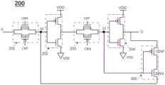
图2为本发明一实施例动态D触发器的电路结构示意图。如图2所示,动态D触发器200包括输入端D、输出端Q、时钟信号端CKN、时钟信号端CKP、第一数据传输单元201、第一锁存单元202、第二数据传输单元203、第二锁存单元204以及漏电补偿单元205。第一数据传输单元201、第一锁存单元202、第二数据传输单元203、第二锁存单元204依次串联连接在输入端D和输出端Q之间,第一数据传输单元201和第一锁存单元202之间形成第一节点S0,第二数据传输单元203和第二锁存单元204之间形成第二节点S1。漏电补偿单元205电性连接在第一节点S0、第二节点S1以及输出端Q之间。其中,输入端D用于输入数据,输出端用于输出数据,时钟信号端CKN以及时钟信号端CKP用于提供时钟信号CKN以及时钟信号CKP,时钟信号CKN与时钟信号CKP为反相时钟信号。FIG. 2 is a schematic diagram of a circuit structure of a dynamic D flip-flop according to an embodiment of the present invention. As shown in FIG. 2 , the dynamic D flip-
具体的,如图2所示,动态D触发器200的第一数据传输单元201为传输门结构,数据传输单元201包括并联连接的PMOS晶体管201P以及NMOS晶体管201N。其中,PMOS晶体管201P的源极端与NMOS晶体管201N的源极端并联连接,并电性连接至动态D触发器200的输入端D,PMOS晶体管201P的漏极端与NMOS晶体管201N的漏极端并联连接,并电性连接至第一节点S0。NMOS晶体管201N的栅极端电性连接至时钟信号CKN,PMOS晶体管201P的栅极端电性连接至时钟信号CKP。当CKP为低电平时,CKN为高电平,PMOS晶体管201P与NMOS晶体管201N均为导通状态,动态D触发器200输入端D的数据通过第一数据传输单元201传送至第一节点S0。当CKP为高电平时,CKN为低电平,PMOS晶体管201P与NMOS晶体管201N均为不导通状态,动态D触发器200输入端D的数据不能通过第一数据传输单元201向第一节点S0进行传送。在本实施例中,第一数据传输单元201以传输门结构进行举例,当然,也可以是其他形式的数据传输单元,只要能够在时钟信号的控制下实现开关功能即可,本发明并不以此为限。Specifically, as shown in FIG. 2 , the first
继续参照图2所示,动态D触发器200的第一锁存单元202为反相器结构,第一锁存单元202既可以利用其寄生电容暂存从第一数据传输单元201传输过来的数据,即第一节点S0处的数据,还可以将第一节点S0处的数据反相,并传送至第二数据传输单元203。Continuing to refer to FIG. 2 , the
如图2所示,动态D触发器200的第二数据传输单元202为传输门结构,第二数据传输单元203包括并联连接的PMOS晶体管203P以及NMOS晶体管203N。其中,PMOS晶体管203P的源极端与NMOS晶体管203N的源极端并联连接,并电性连接至第一锁存单元202,PMOS晶体管203P的漏极端与NMOS晶体管203N的漏极端并联连接,并电性连接至第二节点S1。NMOS晶体管203N的栅极端电性连接至时钟信号CKP,PMOS晶体管203P的栅极端电性连接至时钟信号CKN。当CKN为低电平时,CKP为高电平,PMOS晶体管203P与NMOS晶体管203N均为导通状态,第一锁存单元202输出的数据通过第二数据传输单元203传送至第二节点S1。当CKN为高电平时,CKP为低电平,PMOS晶体管203P与NMOS晶体管203N均为不导通状态,动态D触发器200输入端D的数据不能通过第二数据传输单元203向第二节点S1进行传送。在本实施例中,第二数据传输单元203以传输门结构进行举例,当然,也可以是其他形式的数据传输单元,只要能够在时钟信号的控制下实现开关功能即可,本发明并不以此为限。As shown in FIG. 2 , the second
继续参照图2所示,动态D触发器200的第二锁存单元204为反相器结构,第二锁存单元204与第一锁存单元202一样,既可以利用其寄生电容暂存从第二数据传输单元203传输过来的数据,即第二节点S1处的数据,还可以将第二节点S1处的数据反相,并传送至动态D触发器200的输出端Q。Continuing to refer to FIG. 2 , the
由此可见,第一数据传输单元201以及第二数据传输单元203受到反相时钟信号的控制,即第一数据传输单元201以及第二数据传输单元203不会同时导通和/或截止,动态D触发器200中的第一锁存单元202和第二锁存单元204根据时钟信号起到数据寄存的作用。且,动态D触发器200输入端D的数据经过第一锁存单元202和第二锁存单元204的反相,使得输出端Q的数据与输入端D的数据同相。同时,第一锁存单元202和第二锁存单元204还可以起到提高数据驱动能力的作用。It can be seen that the first
如图2所示,动态D触发器200还包括漏电补偿单元205。在本实施例中,漏电补偿单元205包括PMOS晶体管205P以及NMOS晶体管205N,PMOS晶体管205P以及NMOS晶体管205N串联连接在输出端Q以及第一节点S0之间。PMOS晶体管205P的源极端电性连接至输出端Q,PMOS晶体管205P的漏极端电性连接至NMOS晶体管205N的漏极端,NMOS晶体管205N的源极端电性连接至第一节点S0,PMOS晶体管205P以及NMOS晶体管205N的栅极端并联连接在一起,并电性连接至第二节点S1。As shown in FIG. 2 , the dynamic D flip-
由于PMOS晶体管205P以及NMOS晶体管205N的栅极端同样都电性连接至第二节点S1,在相同电平的信号驱动下,PMOS晶体管205P以及NMOS晶体管205N不会同时导通,只能有一个处于导通状态,另一个处于截止状态。例如,当第二节点S1处的电位为高电平时,PMOS晶体管205P处于截止状态,而NMOS晶体管205N处于导通状态;当第二节点S1处的电位为低电平时,PMOS晶体管205P处于导通状态,而NMOS晶体管205N处于截止状态。因此,漏电补偿单元205可以将输出端Q的漏电电流反馈至第一节点S0处的同时,增加第二节点S1处的寄生电容,既可以补偿第一节点S0处的漏电电流,又可以增加第二节点S1处的寄生电容,从而提高第一节点S0及第二节点S1处数据存储的稳定性,增强数据的正确性和安全性。Since the gate terminals of the PMOS transistor 205P and the
实施例二:Embodiment 2:
图3为本发明又一实施例动态D触发器的电路结构示意图。图3为本发明一实施例动态D触发器的电路结构示意图。如图3所示,动态D触发器200包括输入端D、输出端Q、时钟信号端CKN、时钟信号端CKP、第一数据传输单元201、第一锁存单元202、第二数据传输单元203、第二锁存单元204以及漏电补偿单元205。第一数据传输单元201、第一锁存单元202、第二数据传输单元203、第二锁存单元204依次串联连接在输入端D和输出端Q之间,第一数据传输单元201和第一锁存单元202之间形成第一节点S0,第二数据传输单元203和第二锁存单元204之间形成第二节点S1。漏电补偿单元205电性连接在第一节点S0、第二节点S1以及输出端Q之间。其中,输入端D用于输入数据,输出端用于输出数据,时钟信号端CKN以及时钟信号端CKP用于提供时钟信号CKN以及时钟信号CKP,时钟信号CKN与时钟信号CKP为反相时钟信号。FIG. 3 is a schematic diagram of a circuit structure of a dynamic D flip-flop according to another embodiment of the present invention. FIG. 3 is a schematic diagram of a circuit structure of a dynamic D flip-flop according to an embodiment of the present invention. As shown in FIG. 3 , the dynamic D flip-
具体的,如图3所示,动态D触发器200的第一数据传输单元201为传输门结构,数据传输单元201包括并联连接的PMOS晶体管201P以及NMOS晶体管201N。其中,PMOS晶体管201P的源极端与NMOS晶体管201N的源极端并联连接,并电性连接至动态D触发器200的输入端D,PMOS晶体管201P的漏极端与NMOS晶体管201N的漏极端并联连接,并电性连接至第一节点S0。NMOS晶体管201N的栅极端电性连接至时钟信号CKN,PMOS晶体管201P的栅极端电性连接至时钟信号CKP。当CKP为低电平时,CKN为高电平,PMOS晶体管201P与NMOS晶体管201N均为导通状态,动态D触发器200输入端D的数据通过第一数据传输单元201传送至第一节点S0。当CKP为高电平时,CKN为低电平,PMOS晶体管201P与NMOS晶体管201N均为不导通状态,动态D触发器200输入端D的数据不能通过第一数据传输单元201向第一节点S0进行传送。在本实施例中,第一数据传输单元201以传输门结构进行举例,当然,也可以是其他形式的数据传输单元,只要能够在时钟信号的控制下实现开关功能即可,本发明并不以此为限。Specifically, as shown in FIG. 3 , the first
继续参照图3所示,动态D触发器200的第一锁存单元202为反相器结构,第一锁存单元202既可以利用其寄生电容暂存从第一数据传输单元201传输过来的数据,即第一节点S0处的数据,还可以将第一节点S0处的数据反相,并传送至第二数据传输单元203。Continuing to refer to FIG. 3 , the
如图3所示,动态D触发器200的第二数据传输单元202为传输门结构,第二数据传输单元203包括并联连接的PMOS晶体管203P以及NMOS晶体管203N。其中,PMOS晶体管203P的源极端与NMOS晶体管203N的源极端并联连接,并电性连接至第一锁存单元202,PMOS晶体管203P的漏极端与NMOS晶体管203N的漏极端并联连接,并电性连接至第二节点S1。NMOS晶体管203N的栅极端电性连接至时钟信号CKP,PMOS晶体管203P的栅极端电性连接至时钟信号CKN。当CKN为低电平时,CKP为高电平,PMOS晶体管203P与NMOS晶体管203N均为导通状态,第一锁存单元202输出的数据通过第二数据传输单元203传送至第二节点S1。当CKN为高电平时,CKP为低电平,PMOS晶体管203P与NMOS晶体管203N均为不导通状态,动态D触发器200输入端D的数据不能通过第二数据传输单元203向第二节点S1进行传送。在本实施例中,第二数据传输单元203以传输门结构进行举例,当然,也可以是其他形式的数据传输单元,只要能够在时钟信号的控制下实现开关功能即可,本发明并不以此为限。As shown in FIG. 3 , the second
继续参照图3所示,动态D触发器200的第二锁存单元204为反相器结构,第二锁存单元204与第一锁存单元202一样,既可以利用其寄生电容暂存从第二数据传输单元203传输过来的数据,即第二节点S1处的数据,还可以将第二节点S1处的数据反相,并传送至动态D触发器200的输出端Q。3, the
由此可见,第一数据传输单元201以及第二数据传输单元203受到反相时钟信号的控制,即第一数据传输单元201以及第二数据传输单元203不会同时导通和/或截止,动态D触发器200中的第一锁存单元202和第二锁存单元204根据时钟信号起到数据寄存的作用。且,动态D触发器200输入端D的数据经过第一锁存单元202和第二锁存单元204的反相,使得输出端Q的数据与输入端D的数据同相。同时,第一锁存单元202和第二锁存单元204还可以起到提高数据驱动能力的作用。It can be seen that the first
如图3所示,动态D触发器200还包括漏电补偿单元205。与图3所示实施例不同之处在于,在本实施例中,漏电补偿单元205包括PMOS晶体管205P以及NMOS晶体管205N,PMOS晶体管205P以及NMOS晶体管205N串联连接在输出端Q以及第一节点S0之间。PMOS晶体管205P的源极端电性连接至第一节点S0,PMOS晶体管205P的漏极端电性连接至NMOS晶体管205N的漏极端,NMOS晶体管205N的源极端电性连接至输出端Q,PMOS晶体管205P以及NMOS晶体管205N的栅极端并联连接在一起,并电性连接至第二节点S1。As shown in FIG. 3 , the dynamic D flip-
由于PMOS晶体管205P以及NMOS晶体管205N的栅极端同样都电性连接至第二节点S1,在相同电平的信号驱动下,PMOS晶体管205P以及NMOS晶体管205N不会同时导通,只能有一个处于导通状态,另一个处于截止状态。例如,当第二节点S1处的电位为高电平时,PMOS晶体管205P处于截止状态,而NMOS晶体管205N处于导通状态;当第二节点S1处的电位为低电平时,PMOS晶体管205P处于导通状态,而NMOS晶体管205N处于截止状态。因此,漏电补偿单元205可以将输出端Q的漏电电流反馈至第一节点S0处的同时,增加第二节点S1处的寄生电容,既可以补偿第一节点S0处的漏电电流,又可以增加第二节点S1处的寄生电容,从而提高第一节点S0及第二节点S1处数据存储的稳定性,增强数据的正确性和安全性。Since the gate terminals of the PMOS transistor 205P and the
本发明还提供一种数据运算单元,图4为本发明数据运算单元的结构示意图。如图4所示,数据运算单元400包括控制电路401、运算电路402以及多个动态寄存200。控制电路401对动态寄存200中的数据进行刷新并从动态寄存200中读取数据,运算电路402对读取的数据进行运算,再由控制电路401将运算结果输出。The present invention also provides a data operation unit, and FIG. 4 is a schematic structural diagram of the data operation unit of the present invention. As shown in FIG. 4 , the
本发明还提供一种芯片,图5为本发明芯片的结构示意图。如图5所示,芯片500包括控制单元501,以及一个或多个数据运算单元400。控制单元501向数据运算单元400输入数据并将数据运算单元400输出的数据进行处理。The present invention also provides a chip, and FIG. 5 is a schematic structural diagram of the chip of the present invention. As shown in FIG. 5 , the
本发明还提供一种算力板,图6为本发明算力板的结构示意图。如图6所示,每一个算力板600上包括一个或多个芯片500,对计算设备下发的工作数据进行大规模运算。The present invention also provides a computing power board, and FIG. 6 is a schematic structural diagram of the computing power board of the present invention. As shown in FIG. 6 , each
本发明还提供一种计算设备,所述计算设备优选用于挖掘虚拟数字货币的运算,当然所述计算设备也可以用于其他任何海量运算。图7为本发明计算设备的结构示意图。如图7所示,每一个计算设备700包括连接板701、控制板702、散热器703、电源板704,以及一个或多个算力板600。控制板702通过连接板701与算力板600连接,散热器703设置在算力板600的周围。电源板704用于向所述连接板701、控制板702、散热器703以及算力板600提供电源。The present invention also provides a computing device. The computing device is preferably used for mining virtual digital currency. Of course, the computing device can also be used for any other massive computing. FIG. 7 is a schematic structural diagram of a computing device of the present invention. As shown in FIG. 7 , each
需要说明的是,在本发明的描述中,术语“横向”、“纵向”、“上”、“下”、“前”、“后”、“左”、“右”、“竖直”、“水平”、“顶”、“底”、“内”、“外”等指示的方位或位置关系为基于附图所示的方位或位置关系,仅是为了便于描述本发明和简化描述,并不是指示或暗示所指的装置或元件必须具有特定的方位、以特定的方位构造和操作,因此不能理解为对本发明的限制。It should be noted that in the description of the present invention, the terms "horizontal", "longitudinal", "upper", "lower", "front", "rear", "left", "right", "vertical", The orientation or positional relationship indicated by "horizontal", "top", "bottom", "inside", "outside", etc. is based on the orientation or positional relationship shown in the accompanying drawings, and is only for the convenience of describing the present invention and simplifying the description, and It is not indicated or implied that the indicated device or element must have a particular orientation, be constructed and operate in a particular orientation, and therefore should not be construed as limiting the invention.
换言之,本发明还可有其它多种实施例,在不背离本发明精神及其实质的情况下,熟悉本领域的技术人员当可根据本发明作出各种相应的改变和变形,但这些相应的改变和变形都应属于本发明所附的权利要求的保护范围。In other words, the present invention can also have other various embodiments, without departing from the spirit and essence of the present invention, those skilled in the art can make various corresponding changes and modifications according to the present invention, but these corresponding Changes and deformations should belong to the protection scope of the appended claims of the present invention.
Claims (12)
Translated fromChinesePriority Applications (1)
| Application Number | Priority Date | Filing Date | Title |
|---|---|---|---|
| CN201910948079.3ACN110677141B (en) | 2019-09-30 | 2019-09-30 | Dynamic D trigger, data operation unit, chip, power board and computing device |
Applications Claiming Priority (1)
| Application Number | Priority Date | Filing Date | Title |
|---|---|---|---|
| CN201910948079.3ACN110677141B (en) | 2019-09-30 | 2019-09-30 | Dynamic D trigger, data operation unit, chip, power board and computing device |
Publications (2)
| Publication Number | Publication Date |
|---|---|
| CN110677141Atrue CN110677141A (en) | 2020-01-10 |
| CN110677141B CN110677141B (en) | 2025-08-12 |
Family
ID=69080948
Family Applications (1)
| Application Number | Title | Priority Date | Filing Date |
|---|---|---|---|
| CN201910948079.3AActiveCN110677141B (en) | 2019-09-30 | 2019-09-30 | Dynamic D trigger, data operation unit, chip, power board and computing device |
Country Status (1)
| Country | Link |
|---|---|
| CN (1) | CN110677141B (en) |
Cited By (4)
| Publication number | Priority date | Publication date | Assignee | Title |
|---|---|---|---|---|
| WO2022121365A1 (en)* | 2020-12-09 | 2022-06-16 | 深圳比特微电子科技有限公司 | Dynamic d flip-flop, register, chip, and data processing apparatus |
| CN115118253A (en)* | 2022-07-14 | 2022-09-27 | 上海嘉楠捷思信息技术有限公司 | Dynamic latch, dynamic D trigger, data operation unit, chip, force calculation board and computing equipment |
| WO2023051255A1 (en)* | 2021-09-30 | 2023-04-06 | 北京比特大陆科技有限公司 | Dynamic latch, semiconductor chip, computing power board, and computing device |
| TWI853582B (en)* | 2022-07-14 | 2024-08-21 | 大陸商上海嘉楠捷思信息技術有限公司 | Dynamic d flip-flop, data operation unit, chip, hash board and computing device |
Citations (11)
| Publication number | Priority date | Publication date | Assignee | Title |
|---|---|---|---|---|
| US4896296A (en)* | 1985-03-04 | 1990-01-23 | Lattice Semiconductor Corporation | Programmable logic device configurable input/output cell |
| US5929687A (en)* | 1995-11-08 | 1999-07-27 | Matsushita Electric Industrial Co., Ltd. | Signal transmitting circuit, signal receiving circuit, signal transmitting/receiving circuit, signal transmitting method, signal receiving method signal transmitting/receiving method, semiconductor integrated circuit, and control method thereof |
| US20060033530A1 (en)* | 2004-08-16 | 2006-02-16 | Jin-Ho Seo | Digital circuits having current mirrors and reduced leakage current |
| CN101183866A (en)* | 2006-11-16 | 2008-05-21 | 国际商业机器公司 | Hybrid keeper circuit for dynamic logic |
| US20080253180A1 (en)* | 2005-07-05 | 2008-10-16 | Michel Nicolaidis | Hardened Memory Cell |
| US20110157964A1 (en)* | 2009-12-30 | 2011-06-30 | Mcpartland Richard J | Memory Cell Using Leakage Current Storage Mechanism |
| US8115531B1 (en)* | 2008-03-31 | 2012-02-14 | Lsi Corporation | D flip-flop having enhanced immunity to single-event upsets and method of operation thereof |
| KR20140077464A (en)* | 2012-12-14 | 2014-06-24 | 금오공과대학교 산학협력단 | Tspc dynamic flip flop having leakage current compensation function |
| CN208608968U (en)* | 2018-06-25 | 2019-03-15 | 北京嘉楠捷思信息技术有限公司 | Positive feedback dynamic D trigger, and data operation unit, chip, force calculation board and computing equipment using positive feedback dynamic D trigger |
| CN110289846A (en)* | 2019-06-27 | 2019-09-27 | 北京大学深圳研究生院 | A flip-flop with data hold function |
| CN210867618U (en)* | 2019-09-30 | 2020-06-26 | 杭州嘉楠耘智信息科技有限公司 | Dynamic D trigger, data operation unit, chip, force calculation board and computing equipment |
- 2019
- 2019-09-30CNCN201910948079.3Apatent/CN110677141B/enactiveActive
Patent Citations (12)
| Publication number | Priority date | Publication date | Assignee | Title |
|---|---|---|---|---|
| US4896296A (en)* | 1985-03-04 | 1990-01-23 | Lattice Semiconductor Corporation | Programmable logic device configurable input/output cell |
| US5929687A (en)* | 1995-11-08 | 1999-07-27 | Matsushita Electric Industrial Co., Ltd. | Signal transmitting circuit, signal receiving circuit, signal transmitting/receiving circuit, signal transmitting method, signal receiving method signal transmitting/receiving method, semiconductor integrated circuit, and control method thereof |
| US20060033530A1 (en)* | 2004-08-16 | 2006-02-16 | Jin-Ho Seo | Digital circuits having current mirrors and reduced leakage current |
| US20080253180A1 (en)* | 2005-07-05 | 2008-10-16 | Michel Nicolaidis | Hardened Memory Cell |
| CN101183866A (en)* | 2006-11-16 | 2008-05-21 | 国际商业机器公司 | Hybrid keeper circuit for dynamic logic |
| US20080116938A1 (en)* | 2006-11-16 | 2008-05-22 | Ngo Hung C | Hybrid Keeper Circuit for Dynamic Logic |
| US8115531B1 (en)* | 2008-03-31 | 2012-02-14 | Lsi Corporation | D flip-flop having enhanced immunity to single-event upsets and method of operation thereof |
| US20110157964A1 (en)* | 2009-12-30 | 2011-06-30 | Mcpartland Richard J | Memory Cell Using Leakage Current Storage Mechanism |
| KR20140077464A (en)* | 2012-12-14 | 2014-06-24 | 금오공과대학교 산학협력단 | Tspc dynamic flip flop having leakage current compensation function |
| CN208608968U (en)* | 2018-06-25 | 2019-03-15 | 北京嘉楠捷思信息技术有限公司 | Positive feedback dynamic D trigger, and data operation unit, chip, force calculation board and computing equipment using positive feedback dynamic D trigger |
| CN110289846A (en)* | 2019-06-27 | 2019-09-27 | 北京大学深圳研究生院 | A flip-flop with data hold function |
| CN210867618U (en)* | 2019-09-30 | 2020-06-26 | 杭州嘉楠耘智信息科技有限公司 | Dynamic D trigger, data operation unit, chip, force calculation board and computing equipment |
Non-Patent Citations (1)
| Title |
|---|
| MARTIN HANSSON: "A LEAKAGE COMPENSATION TECHNIQUE FOR DYNAMIC LATCHES AND FLIP-FLOPS IN NANO-SCALE CMOS",A LEAKAGE COMPENSATION TECHNIQUE FOR DYNAMIC LATCHES AND FLIP-FLOPS IN NANO-SCALE CMOS, 15 January 2007 (2007-01-15), pages 1 - 2* |
Cited By (6)
| Publication number | Priority date | Publication date | Assignee | Title |
|---|---|---|---|---|
| WO2022121365A1 (en)* | 2020-12-09 | 2022-06-16 | 深圳比特微电子科技有限公司 | Dynamic d flip-flop, register, chip, and data processing apparatus |
| WO2023051255A1 (en)* | 2021-09-30 | 2023-04-06 | 北京比特大陆科技有限公司 | Dynamic latch, semiconductor chip, computing power board, and computing device |
| CN115118253A (en)* | 2022-07-14 | 2022-09-27 | 上海嘉楠捷思信息技术有限公司 | Dynamic latch, dynamic D trigger, data operation unit, chip, force calculation board and computing equipment |
| WO2024012031A1 (en)* | 2022-07-14 | 2024-01-18 | 上海嘉楠捷思信息技术有限公司 | Dynamic latch, dynamic d flip-flop, data operation unit, chip, hash board, and computing device |
| TWI853581B (en)* | 2022-07-14 | 2024-08-21 | 大陸商上海嘉楠捷思信息技術有限公司 | Dynamic latch, dynamic d flip-flop, data operation unit, chip, hash board and computing device |
| TWI853582B (en)* | 2022-07-14 | 2024-08-21 | 大陸商上海嘉楠捷思信息技術有限公司 | Dynamic d flip-flop, data operation unit, chip, hash board and computing device |
Also Published As
| Publication number | Publication date |
|---|---|
| CN110677141B (en) | 2025-08-12 |
Similar Documents
| Publication | Publication Date | Title |
|---|---|---|
| CN211209690U (en) | Dynamic latch, data operation unit, chip, force calculation board and computing equipment | |
| CN110706731A (en) | Leakage compensation dynamic register, data operation unit, chip, computing power board and computing equipment | |
| CN110677141A (en) | Dynamic D flip-flops, data operation units, chips, computing power boards and computing equipment | |
| CN105471410A (en) | Flip-flops with low clock power | |
| US20250150068A1 (en) | Dynamic latch, dynamic d flip-flop, data operation unit, chip, hash board, and computing device | |
| CN110675909A (en) | Dynamic register, data operation unit, chip, force calculation board and computing equipment | |
| US11251781B2 (en) | Dynamic D flip-flop, data operation unit, chip, hash board and computing device | |
| US20250158600A1 (en) | Dynamic d flip-flop, data operation unit, chip, hash board and computing device | |
| US11409314B2 (en) | Full swing voltage conversion circuit and operation unit, chip, hash board, and computing device using same | |
| CN110708041A (en) | Electric leakage feedback dynamic D trigger, data operation unit, chip, force calculation board and computing equipment | |
| US10868524B2 (en) | Semiconductor circuit and semiconductor circuit layout system | |
| CN210865632U (en) | Dynamic register, data operation unit, chip, force calculation board and computing equipment | |
| CN210867618U (en) | Dynamic D trigger, data operation unit, chip, force calculation board and computing equipment | |
| CN210899130U (en) | Dynamic latch, data operation unit, chip, force calculation board and computing equipment | |
| CN210899105U (en) | Electric leakage feedback dynamic D trigger, data operation unit, chip, force calculation board and computing equipment | |
| CN110690887A (en) | Dynamic latch, data operation unit, chip, computing power board and computing equipment | |
| CN115589218A (en) | Dynamic latch, data operation unit, chip, computing power board and computing equipment | |
| CN115001456A (en) | Dynamic latch, data operation unit, chip, computing force board and computing equipment | |
| CN218071463U (en) | Dynamic latch, dynamic D trigger, data operation unit, chip, force calculation board and computing equipment | |
| CN218071462U (en) | Dynamic latch, data operation unit, chip, force calculation board and computing equipment | |
| CN210865633U (en) | Electric leakage compensation dynamic register, data arithmetic unit, chip, force calculation board and computing equipment | |
| CN218183324U (en) | Dynamic D trigger, data operation unit, chip, force calculation board and computing equipment | |
| CN218071464U (en) | Dynamic latch, data operation unit, chip, force calculation board and computing equipment | |
| CN115001476A (en) | Register, arithmetic unit, chip, and computing device | |
| HK40070682A (en) | Leakage compensation dynamic register, data computing unit, chip, computing power board, and computing apparatus |
Legal Events
| Date | Code | Title | Description |
|---|---|---|---|
| PB01 | Publication | ||
| PB01 | Publication | ||
| SE01 | Entry into force of request for substantive examination | ||
| SE01 | Entry into force of request for substantive examination | ||
| GR01 | Patent grant | ||
| GR01 | Patent grant |