CN110676235A - A new type of power MOS module structure that is easy to expand - Google Patents
A new type of power MOS module structure that is easy to expandDownload PDFInfo
- Publication number
- CN110676235A CN110676235ACN201911022020.8ACN201911022020ACN110676235ACN 110676235 ACN110676235 ACN 110676235ACN 201911022020 ACN201911022020 ACN 201911022020ACN 110676235 ACN110676235 ACN 110676235A
- Authority
- CN
- China
- Prior art keywords
- copper foil
- power mos
- modules
- control terminal
- mos
- Prior art date
- Legal status (The legal status is an assumption and is not a legal conclusion. Google has not performed a legal analysis and makes no representation as to the accuracy of the status listed.)
- Granted
Links
Images


Classifications
- H—ELECTRICITY
- H01—ELECTRIC ELEMENTS
- H01L—SEMICONDUCTOR DEVICES NOT COVERED BY CLASS H10
- H01L25/00—Assemblies consisting of a plurality of semiconductor or other solid state devices
- H01L25/03—Assemblies consisting of a plurality of semiconductor or other solid state devices all the devices being of a type provided for in a single subclass of subclasses H10B, H10D, H10F, H10H, H10K or H10N, e.g. assemblies of rectifier diodes
- H01L25/04—Assemblies consisting of a plurality of semiconductor or other solid state devices all the devices being of a type provided for in a single subclass of subclasses H10B, H10D, H10F, H10H, H10K or H10N, e.g. assemblies of rectifier diodes the devices not having separate containers
- H01L25/07—Assemblies consisting of a plurality of semiconductor or other solid state devices all the devices being of a type provided for in a single subclass of subclasses H10B, H10D, H10F, H10H, H10K or H10N, e.g. assemblies of rectifier diodes the devices not having separate containers the devices being of a type provided for in group subclass H10D
- H—ELECTRICITY
- H01—ELECTRIC ELEMENTS
- H01L—SEMICONDUCTOR DEVICES NOT COVERED BY CLASS H10
- H01L23/00—Details of semiconductor or other solid state devices
- H01L23/28—Encapsulations, e.g. encapsulating layers, coatings, e.g. for protection
- H01L23/31—Encapsulations, e.g. encapsulating layers, coatings, e.g. for protection characterised by the arrangement or shape
- H01L23/3107—Encapsulations, e.g. encapsulating layers, coatings, e.g. for protection characterised by the arrangement or shape the device being completely enclosed
- H01L23/3121—Encapsulations, e.g. encapsulating layers, coatings, e.g. for protection characterised by the arrangement or shape the device being completely enclosed a substrate forming part of the encapsulation
- H—ELECTRICITY
- H01—ELECTRIC ELEMENTS
- H01L—SEMICONDUCTOR DEVICES NOT COVERED BY CLASS H10
- H01L23/00—Details of semiconductor or other solid state devices
- H01L23/48—Arrangements for conducting electric current to or from the solid state body in operation, e.g. leads, terminal arrangements ; Selection of materials therefor
- H01L23/488—Arrangements for conducting electric current to or from the solid state body in operation, e.g. leads, terminal arrangements ; Selection of materials therefor consisting of soldered or bonded constructions
- H—ELECTRICITY
- H01—ELECTRIC ELEMENTS
- H01L—SEMICONDUCTOR DEVICES NOT COVERED BY CLASS H10
- H01L2224/00—Indexing scheme for arrangements for connecting or disconnecting semiconductor or solid-state bodies and methods related thereto as covered by H01L24/00
- H01L2224/01—Means for bonding being attached to, or being formed on, the surface to be connected, e.g. chip-to-package, die-attach, "first-level" interconnects; Manufacturing methods related thereto
- H01L2224/42—Wire connectors; Manufacturing methods related thereto
- H01L2224/47—Structure, shape, material or disposition of the wire connectors after the connecting process
- H01L2224/49—Structure, shape, material or disposition of the wire connectors after the connecting process of a plurality of wire connectors
- H01L2224/491—Disposition
- H01L2224/4911—Disposition the connectors being bonded to at least one common bonding area, e.g. daisy chain
- H01L2224/49111—Disposition the connectors being bonded to at least one common bonding area, e.g. daisy chain the connectors connecting two common bonding areas, e.g. Litz or braid wires
Landscapes
- Engineering & Computer Science (AREA)
- Microelectronics & Electronic Packaging (AREA)
- Power Engineering (AREA)
- Physics & Mathematics (AREA)
- Condensed Matter Physics & Semiconductors (AREA)
- General Physics & Mathematics (AREA)
- Computer Hardware Design (AREA)
- Power Conversion In General (AREA)
- Cooling Or The Like Of Semiconductors Or Solid State Devices (AREA)
Abstract
Translated fromChinese
Description
Translated fromChinese技术领域technical field
本发明涉及功率模组领域,特别是一种便于扩展的新型功率MOS模组结构。The invention relates to the field of power modules, in particular to a novel power MOS module structure that is easy to expand.
背景技术Background technique
DBC板在电力电子模块技术中,主要是作为各种芯片如IGBT芯片、Diode芯片、电阻、SiC芯片等的承载体,DBC板通过表面覆铜层完成芯片部分连接极或者连接面的连接,功能近似于PCB板。随着电子电力技术的发展,MOS管以其高频性能好、开关损耗小、输出阻抗高、驱动功率小等优点被越来越广泛的应用。功率MOS模块是MOS管按一定的功能组合再灌封成一个模块,其功率MOS模块使用时候通常需要配合其他外部器件进行使用,现有的功率模块集成度不高,输出功率较小,模块利用率低,输入输出端子较多,结构复杂,功率模块的制作体积大,由于功率MOS模块在DBC板上的布线问题,与外部电连接复杂模块内产生较大的寄生电容和电感,在功率MOS模块的关断和开启过程中,MOS管栅极将产生电压尖峰脉冲,损坏器件,功率MOS模块易烧毁,影响整个电路的正常工作。In the power electronic module technology, the DBC board is mainly used as the carrier of various chips such as IGBT chips, Diode chips, resistors, SiC chips, etc. The DBC board completes the connection of the connecting poles or connecting surfaces of the chip part through the surface copper cladding layer. Similar to a PCB board. With the development of electronic power technology, MOS tube is more and more widely used for its advantages of good high frequency performance, low switching loss, high output impedance and low driving power. Power MOS modules are MOS tubes that are re-potted into a module according to a certain combination of functions. When using power MOS modules, they usually need to be used with other external devices. The existing power modules have low integration and low output power. Due to the wiring problem of the power MOS module on the DBC board, large parasitic capacitance and inductance are generated in the external electrical connection complex module, and the power MOS module has a large volume. In the process of turning off and turning on the module, the gate of the MOS tube will generate voltage spikes, which will damage the device, and the power MOS module will be easily burned, which will affect the normal operation of the entire circuit.
发明内容SUMMARY OF THE INVENTION
本发明的目的在于:提出一种便于扩展的新型功率MOS模组结构,解决了上述背景技术中的问题。The purpose of the present invention is to propose a novel power MOS module structure that is easy to expand, and solves the above-mentioned problems in the background technology.
本发明采用的技术方案如下:The technical scheme adopted in the present invention is as follows:
本发明公开了一种便于扩展的新型功率MOS模组结构,包括双面覆有铜箔的DBC板,所述DBC板上还设置有两组功率MOS模组,每组功率MOS模组集成了至少2个并联成排的MOS管,每组功率MOS模组的MOS管源极共同连接到一个DBC板上的源极输出端铜箔和1个源极控制端铜箔,漏极连接到DBC板上的漏极输入端铜箔,并且漏极输入端铜箔上还引出有控制端子,栅极与栅极控制端铜箔连接,每组功率MOS模组的漏极输入端铜箔和源极输出端铜箔上还焊接有主端子,其中一组功率MOS模组连接的源极输出端铜箔与另一组功率MOS模组连接的漏极输入端铜箔连接并且共用一个主端子。The invention discloses a novel power MOS module structure which is easy to expand, including a DBC board covered with copper foil on both sides, and two sets of power MOS modules are further arranged on the DBC board, and each set of power MOS modules integrates At least two MOS transistors in parallel rows, the MOS transistor sources of each group of power MOS modules are commonly connected to the source output copper foil and one source control copper foil on a DBC board, and the drain is connected to the DBC The copper foil of the drain input end on the board, and the control terminal is also drawn out from the copper foil of the drain input end, the gate is connected to the copper foil of the gate control end, and the copper foil of the drain input end of each group of power MOS modules and the source A main terminal is also welded on the copper foil of the output end, wherein the copper foil of the source output end connected to one group of power MOS modules is connected to the copper foil of the drain input end connected to the other group of power MOS modules and shares a main terminal.
在本发明中,每组功率MOS模组集成了至少2个并联成排的MOS管,MOS管布局紧凑,集成度高,能够输出更大的功率;每组功率MOS模组的漏极输入端铜箔引出有控制端子,源极连接1个源极控制端铜箔用于外接驱动板电路,功率MOS模组的漏极输入端铜箔和源极输出端铜箔上还焊接有主端子,用于连接大电流输出回路,功率MOS模组的源极输出回路和控制端分离,避免了与源极大电流输出回路之间的相互影响,降低电压和电流的尖峰对整个电路的影响,防止器件烧坏;整个DBC板上的MOS管布线紧凑,有效降低寄生电感和电容等。在本发明中,其中一组功率MOS模组连接的源极输出端铜箔与另一组功率MOS模组连接的漏极输入端铜箔连接,并且共同连接一个主端子,该主端子设置在DBC板的一侧与外部Vo连接,DBC板的另一侧还设置有两个主端子分别与V+、V-连接,外接V+的主端子焊接在上述其中一组功率MOS模组的漏极输入端铜箔,外接V-的主端子焊接在上述另一组功率MOS模组的源极输出端铜箔上,采用三个主端子的小型化DBC板,外接大电流输出回路,其结构简单,简化布线,可应用于电机控制,BMS场合,通过对DBC内部布线的改变,实现模块的多功能化。In the present invention, each group of power MOS modules integrates at least two parallel MOS transistors, the MOS transistors have compact layout, high integration, and can output greater power; the drain input end of each group of power MOS modules The copper foil leads to a control terminal, the source is connected to a source control terminal copper foil for external drive board circuit, and the main terminal is also welded on the drain input copper foil and the source output copper foil of the power MOS module. It is used to connect the high current output circuit. The source output circuit of the power MOS module is separated from the control terminal, which avoids the interaction with the source maximum current output circuit, reduces the impact of voltage and current spikes on the entire circuit, and prevents the The device is burned out; the MOS tube wiring on the entire DBC board is compact, which effectively reduces parasitic inductance and capacitance. In the present invention, the copper foil of the source output end connected to one group of power MOS modules is connected to the copper foil of the drain input end connected to the other group of power MOS modules, and is jointly connected to a main terminal, and the main terminal is arranged on the One side of the DBC board is connected to the external Vo, and the other side of the DBC board is also provided with two main terminals connected to V+ and V- respectively. The main terminal of the external V+ is welded to the drain input of one of the above-mentioned power MOS modules. The copper foil at the end, the main terminal of the external V- is welded on the copper foil of the source output end of the other group of power MOS modules, the miniaturized DBC board with three main terminals is used, and the high current output circuit is connected externally, and its structure is simple, Simplified wiring can be applied to motor control and BMS applications. By changing the internal wiring of DBC, the module can be multi-functional.
进一步的,每组功率MOS模组又分为至少两个并联的功率MOS小模组,每个功率MOS小模组的MOS管栅极分别连接1个栅极控制端铜箔,每个栅极控制端铜箔均由外部电路控制连接。采用上述结构,两个并联的功率MOS小模组的栅极不直接连接,分别与1个栅极控制端铜箔连接,2个栅极控制端铜箔均由外部电路控制连接,可有效的降低MOS管应用中栅极的电压尖峰脉冲。Further, each group of power MOS modules is further divided into at least two parallel power MOS small modules, the MOS tube gate of each power MOS small module is respectively connected to a gate control terminal copper foil, and each gate The copper foil of the control terminal is controlled and connected by an external circuit. With the above structure, the gates of the two parallel power MOS small modules are not directly connected, but are respectively connected with one gate control terminal copper foil, and the two gate control terminal copper foils are both controlled and connected by an external circuit, which can effectively Reduces voltage spikes at the gate in MOS transistor applications.
进一步的,每个功率MOS小模组集成了至少1个MOS管。采用上述结构,使得功率MOS模组具有更高的集成度,更高的可靠性,适用于更大的功率器件。Further, each power MOS small module integrates at least one MOS transistor. With the above structure, the power MOS module has higher integration and higher reliability, and is suitable for larger power devices.
进一步的,所述每组功率MOS模组的MOS管采用贴片封装在漏极输入端铜箔上。采用上述结构,可以减小功率MOS模组的制作体积,能够满足大电流通过的要求,输出更大的功率,还能够减短电流的通路长度,减小发热。Further, the MOS transistors of the power MOS modules of each group are packaged on the copper foil of the drain input end by SMD. By adopting the above structure, the manufacturing volume of the power MOS module can be reduced, the requirement of high current passing can be met, greater power can be output, and the current path length can be shortened and heat generation can be reduced.
进一步的,所述栅极控制端铜箔和源极控制端铜箔均焊接有辅助端子,所述辅助端子设置在DBC板的两侧,用于与外部驱动板电路连接。采用上述辅助端子,便于功率MOS模组的各个控制端铜箔通过辅助端子与外部电路连接。Further, auxiliary terminals are welded to the gate control terminal copper foil and the source control terminal copper foil, and the auxiliary terminals are arranged on both sides of the DBC board and are used for circuit connection with an external driving board. The use of the above-mentioned auxiliary terminals facilitates the connection of the copper foils of each control end of the power MOS module to the external circuit through the auxiliary terminals.
进一步的,所述DBC板上还设置有热敏电阻,并且在DBC板的一侧还引出有与热敏电阻连接两个引线端子。采用上述结构,对DBC板上的功率MOS模组进行温度监控,以便调节外部散热装置的散热强度。Further, the DBC board is also provided with a thermistor, and two lead terminals connected to the thermistor are also drawn out from one side of the DBC board. With the above structure, the temperature of the power MOS module on the DBC board is monitored, so as to adjust the heat dissipation intensity of the external heat dissipation device.
进一步的,所述功率MOS模组通过环氧树脂塑封料封装在DBC板上。采用上述结构,其导热性能好,便于散热,不易形变,防潮,抗腐蚀性强,相比常规使用硅凝胶密封的场合,在可靠性和寿命方面都会大大的提升,保证内部功率MOS模组及邦线等的良好,可用于大功率电器的功率MOS模组。Further, the power MOS module is encapsulated on the DBC board by epoxy resin molding compound. With the above structure, it has good thermal conductivity, easy to dissipate heat, is not easy to deform, is moisture-proof, and has strong corrosion resistance. Compared with the conventional use of silicone gel sealing, the reliability and service life will be greatly improved, ensuring the internal power MOS module. And the state line, etc. are good, can be used for power MOS modules of high-power electrical appliances.
进一步的,所述MOS管均通过铝带分别与栅极控制端铜箔、源极控制端铜箔和源极输出端铜箔连接。Further, the MOS tubes are connected to the copper foil of the gate control end, the copper foil of the source control end and the copper foil of the source output end respectively through aluminum tapes.
进一步的,所述MOS管均通过邦线分别与栅极控制端铜箔、源极控制端铜箔和源极输出端铜箔连接。Further, the MOS transistors are connected to the copper foil of the gate control end, the copper foil of the source control end and the copper foil of the source output end respectively through the bond wires.
综上所述,由于采用了上述技术方案,本发明的有益效果是:To sum up, due to the adoption of the above-mentioned technical solutions, the beneficial effects of the present invention are:
1、本发明是一种便于扩展的新型功率MOS模组结构,每组功率MOS模组可集成了多个并联成排的MOS管,MOS管采用贴片工艺焊接在DBC板上,布局紧凑,体积小,集成度高,减小发热,满足大电流通过,能够输出更大的功率。1. The present invention is a new type of power MOS module structure that is easy to expand. Each group of power MOS modules can integrate a plurality of MOS tubes in parallel in a row. Small size, high integration, reduce heat generation, meet the flow of large current, and can output more power.
2、本发明是一种便于扩展的新型功率MOS模组结构,功率MOS模组的源极输出回路和控制端分离,避免了与源极大电流输出回路之间的相互影响,降低电压和电流的尖峰对整个电路的影响,防止器件烧坏。2. The present invention is a new type of power MOS module structure that is easy to expand. The source output loop of the power MOS module is separated from the control terminal, which avoids the interaction with the source maximum current output loop and reduces the voltage and current. The impact of the spike on the entire circuit prevents the device from burning out.
3、本发明是一种便于扩展的新型功率MOS模组结构,每组功率MOS模组的MOS管布局紧凑,有效的降低了整个器件的寄生电感、寄生电容等的影响。3. The present invention is a new type of power MOS module structure that is easy to expand. The MOS tube layout of each group of power MOS modules is compact, which effectively reduces the influence of parasitic inductance and parasitic capacitance of the entire device.
4、本发明是一种便于扩展的新型功率MOS模组结构,采用三个主端子的小型化DBC板,外接大电流输出回路,其结构简单,简化布线,可应用于电机控制,BMS场合,实现模块的多功能化。4. The present invention is a new type of power MOS module structure that is easy to expand. It adopts a miniaturized DBC board with three main terminals and an external high-current output circuit. The structure is simple and the wiring is simplified. Realize the multi-function of the module.
5、本发明是一种便于扩展的新型功率MOS模组结构,DBC板上设置热敏电阻对DBC板上的功率MOS模组进行温度监控,以便调整外部散热装置的散热强度。5. The present invention is a new type of power MOS module structure that is easy to expand. A thermistor is arranged on the DBC board to monitor the temperature of the power MOS module on the DBC board, so as to adjust the heat dissipation intensity of the external heat dissipation device.
附图说明Description of drawings
为了更清楚地说明本发明实施例的技术方案,下面将对实施例中所需要使用的附图作简单地介绍,应当理解,以下附图仅示出了本发明的某些实施例,因此不应被看作是对范围的限定,对于本领域普通技术人员来讲,在不付出创造性劳动的前提下,还可以根据这些附图获得其他相关的附图,其中:In order to illustrate the technical solutions of the embodiments of the present invention more clearly, the following briefly introduces the accompanying drawings used in the embodiments. It should be understood that the following drawings only show some embodiments of the present invention, and therefore do not It should be regarded as a limitation of the scope. For those of ordinary skill in the art, other related drawings can also be obtained from these drawings without creative efforts, wherein:
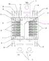
图1是本发明的结构示意图;Fig. 1 is the structural representation of the present invention;
图2是本发明电路原理图;Fig. 2 is the circuit principle diagram of the present invention;
图3是本发明封装后的结构示意图;Fig. 3 is the structural schematic diagram after encapsulation of the present invention;
图4是本发明封装后的背面结构示意图。FIG. 4 is a schematic diagram of the structure of the back of the present invention after encapsulation.
附图标号说明:1-DBC板,2-MOS管,3-漏极输入端铜箔,4-源极输出端铜箔,5-源极控制端铜箔,6-栅极控制端铜箔,7-主端子,8-控制端子,9-辅助端子,10-热敏电阻,11-引线端子。Reference number description: 1-DBC board, 2-MOS tube, 3-drain input copper foil, 4-source output copper foil, 5-source control copper foil, 6-gate control copper foil , 7-main terminal, 8-control terminal, 9-auxiliary terminal, 10-thermistor, 11-lead terminal.
具体实施方式Detailed ways
为了使本发明的目的、技术方案及优点更加清楚明白,以下结合附图及实施例,对本发明进行进一步详细说明。应当理解,此处所描述的具体实施例仅用以解释本发明,并不用于限定本发明,即所描述的实施例仅仅是本发明一部分实施例,而不是全部的实施例。通常在此处附图中描述和示出的本发明实施例的组件可以以各种不同的配置来布置和设计。In order to make the objectives, technical solutions and advantages of the present invention clearer, the present invention will be further described in detail below with reference to the accompanying drawings and embodiments. It should be understood that the specific embodiments described herein are only used to explain the present invention, but not to limit the present invention, that is, the described embodiments are only a part of the embodiments of the present invention, rather than all the embodiments. The components of the embodiments of the invention generally described and illustrated in the drawings herein may be arranged and designed in a variety of different configurations.
本说明书中公开的所有特征,或公开的所有方法或过程中的步骤,除了互相排斥的特征和以外,均可以以任何方式组合。All features disclosed in this specification, or steps in all methods or processes disclosed, may be combined in any way except mutually exclusive features and .
下面结合实施例对本发明的特征和性能作进一步的详细描述。The features and performances of the present invention will be further described in detail below in conjunction with the embodiments.
实施例1Example 1
如图1-4所示,本发明是一种便于扩展的新型功率MOS模组结构,包括双面覆有铜箔的DBC板1,所述DBC板1上还设置有两组功率MOS模组,每组功率MOS模组集成了至少2个并联成排的MOS管2,每组功率MOS模组的MOS管2源极共同连接到一个DBC板1上的源极输出端铜箔4和1个源极控制端铜箔5,漏极连接到DBC板1上的漏极输入端铜箔3,并且漏极输入端铜箔3上还引出有控制端子8,栅极与栅极控制端铜箔6连接,每组功率MOS模组的漏极输入端铜箔3和源极输出端铜箔4上还焊接有主端子7,其中一组功率MOS模组连接的源极输出端铜箔4与另一组功率MOS模组连接的漏极输入端铜箔3连接并且共用一个主端子7。As shown in Figures 1-4, the present invention is a new type of power MOS module structure that is easy to expand, including a
在本发明中,DBC板1采用氮化铝陶瓷基板,其散热效果好,寿命长,在DBC板1上还设置有两组功率MOS模组,每组功率MOS模组集成了至少2个并联成排的MOS管2,可根据需要,集成多个MOS管2,MOS管2布局紧凑,集成度高,能够输出更大的功率;每组功率MOS模组的漏极输入端铜箔3引出有控制端子8,源极连接1个源极控制端铜箔5用于外接驱动板电路,功率MOS模组的漏极输入端铜箔3和源极输出端铜箔4上还焊接有主端子7,用于连接大电流输出回路,功率MOS模组的源极输出回路和控制端分离,避免了与源极大电流输出回路之间的相互影响,降低电压和电流的尖峰对整个电路的影响,防止器件烧坏;整个DBC板1上的MOS管2布线紧凑,有效降低寄生电感和电容等。在本发明中,其中一组功率MOS模组连接的源极输出端铜箔4与另一组功率MOS模组连接的漏极输入端铜箔3连接,并且共同连接一个主端子7,该主端子7设置在DBC板1的一侧与外部Vo连接,DBC板1的另一侧还设置有两个主端子7分别与V+、V-连接,外接V+的主端子7焊接在上述其中一组功率MOS模组的漏极输入端铜箔3,外接V-的主端子7焊接在上述另一组功率MOS模组的源极输出端铜箔4上,采用三个主端子7的小型化DBC板1,外接大电流输出回路,其结构简单,简化布线,可应用于电机控制,BMS场合,通过对DBC内部布线的改变,实现模块的多功能化。In the present invention, the
实施例2Example 2
本实施例是对本发明进一步的说明。This embodiment is a further description of the present invention.
如图1所示,本实施例在实施例1的基础上,本发明一种优选实施例中,每组功率MOS模组又分为至少两个并联的功率MOS小模组,每个功率MOS小模组的MOS管2栅极分别连接1个栅极控制端铜箔6,每个栅极控制端铜箔6均由外部电路控制连接。采用上述结构,两个并联的功率MOS小模组的MOS管2栅极不直接连接,分别与1个栅极控制端铜箔6连接,2个栅极控制端铜箔6均由外部电路控制连接,可有效的降低MOS管2应用中栅极的电压尖峰脉冲。As shown in FIG. 1 , this embodiment is based on
在本发明一种优选实施例中,每个功率MOS小模组集成了至少1个MOS管2。采用上述结构,每个功率MOS小模组可根据实际需求集成1个、2个或者多个MOS管2,使得功率MOS模组具有更高的集成度,更高的可靠性,适用于更大的功率器件。In a preferred embodiment of the present invention, each small power MOS module integrates at least one
实施例3Example 3
本实施例是对本发明进一步的说明。This embodiment is a further description of the present invention.
本实施例在上述的基础上,本发明一种优选实施例中,所述每组功率MOS模组的MOS管2采用贴片封装在漏极输入端铜箔3上。采用上述结构,可以减小功率MOS模组的制作体积,能够满足大电流通过的要求,输出更大的功率,还能够减短电流的通路长度,减小发热。In this embodiment, on the basis of the above, in a preferred embodiment of the present invention, the
实施例4Example 4
本实施例是对本发明进一步的说明。This embodiment is a further description of the present invention.
如图1、3所示,本实施例是在上述实施例的基础上,本发明一种优选实施例中,所述栅极控制端铜箔6和源极控制端铜箔5均焊接有辅助端子9,所述辅助端子9设置在DBC板1的两侧,用于与外部驱动板电路连接。采用上述辅助端子,便于功率MOS模组的各个控制端铜箔通过辅助端子9与外部电路连接。As shown in FIGS. 1 and 3 , this embodiment is based on the above-mentioned embodiment. In a preferred embodiment of the present invention, the gate control
实施例5Example 5
本实施例是对本发明进一步的说明。This embodiment is a further description of the present invention.
如图1所示,本实施例是在上述实施例的基础上,本发明一种优选实施例中,所述DBC板1上还设置有热敏电阻10,并且在DBC板1的一侧还引出有与热敏电阻10连接两个引线端子11。采用上述结构,对DBC板上的功率MOS模组进行温度监控,以便调节外部散热装置的散热强度。As shown in FIG. 1 , this embodiment is based on the above-mentioned embodiment. In a preferred embodiment of the present invention, the
实施例6Example 6
本实施例是对本发明进一步的说明。This embodiment is a further description of the present invention.
本实施例是在上述实施例的基础上,本发明一种优选实施例中,所述功率MOS模组通过环氧树脂塑封料封装在DBC板1上。采用上述结构,其导热性能好,便于散热,不易形变,防潮,抗腐蚀性强,相比常规使用硅凝胶密封的场合,在可靠性和寿命方面都会大大的提升,保证内部功率MOS模组及邦线等的良好,可用于大功率电器的功率MOS模组。This embodiment is based on the above-mentioned embodiment. In a preferred embodiment of the present invention, the power MOS module is encapsulated on the
实施例7Example 7
本实施例是对本发明进一步的说明。This embodiment is a further description of the present invention.
本实施例是在上述实施例的基础上,本发明一种优选实施例中,所述MOS管2均通过铝带分别与栅极控制端铜箔6、源极控制端铜箔5和源极输出端铜箔4连接。This embodiment is based on the above-mentioned embodiment. In a preferred embodiment of the present invention, the
实施例8Example 8
本实施例是对本发明进一步的说明。This embodiment is a further description of the present invention.
本实施例是在上述实施例的基础上,本发明一种优选实施例中,所述MOS管2均通过邦线分别与栅极控制端铜箔6、源极控制端铜箔5和源极输出端铜箔4连接。This embodiment is based on the above-mentioned embodiment. In a preferred embodiment of the present invention, the
以上所述,仅为本发明的优选实施方式,但本发明的保护范围并不局限于此,任何熟悉本领域的技术人员在本发明所揭露的技术范围内,可不经过创造性劳动想到的变化或替换,都应涵盖在本发明的保护范围之内。因此,本发明的保护范围应该以权利要求书所限定的保护范围为准。The above are only the preferred embodiments of the present invention, but the protection scope of the present invention is not limited thereto. Any person skilled in the art may, within the technical scope disclosed by the present invention, think of changes or changes without creative work. Substitutions should be covered within the protection scope of the present invention. Therefore, the protection scope of the present invention should be based on the protection scope defined by the claims.
Claims (9)
Translated fromChinesePriority Applications (1)
| Application Number | Priority Date | Filing Date | Title |
|---|---|---|---|
| CN201911022020.8ACN110676235B (en) | 2019-10-25 | 2019-10-25 | A new power MOS module structure that is easy to expand |
Applications Claiming Priority (1)
| Application Number | Priority Date | Filing Date | Title |
|---|---|---|---|
| CN201911022020.8ACN110676235B (en) | 2019-10-25 | 2019-10-25 | A new power MOS module structure that is easy to expand |
Publications (2)
| Publication Number | Publication Date |
|---|---|
| CN110676235Atrue CN110676235A (en) | 2020-01-10 |
| CN110676235B CN110676235B (en) | 2025-02-07 |
Family
ID=69084334
Family Applications (1)
| Application Number | Title | Priority Date | Filing Date |
|---|---|---|---|
| CN201911022020.8AActiveCN110676235B (en) | 2019-10-25 | 2019-10-25 | A new power MOS module structure that is easy to expand |
Country Status (1)
| Country | Link |
|---|---|
| CN (1) | CN110676235B (en) |
Cited By (2)
| Publication number | Priority date | Publication date | Assignee | Title |
|---|---|---|---|---|
| CN111769081A (en)* | 2020-05-28 | 2020-10-13 | 佛山市国星光电股份有限公司 | Integrated module and power device |
| CN116230660A (en)* | 2023-01-04 | 2023-06-06 | 杭州迈巨微电子有限公司 | Integrated MOS transistor packaging structure and battery management system |
Citations (9)
| Publication number | Priority date | Publication date | Assignee | Title |
|---|---|---|---|---|
| JP2008091945A (en)* | 2007-12-10 | 2008-04-17 | Renesas Technology Corp | Semiconductor device |
| CN101567367A (en)* | 2004-01-28 | 2009-10-28 | 株式会社瑞萨科技 | Semiconductor device |
| CN201417772Y (en)* | 2009-04-02 | 2010-03-03 | 嘉兴斯达微电子有限公司 | Power MOSFET module with gate pole resistance layout |
| US20100182078A1 (en)* | 2009-01-22 | 2010-07-22 | Stmicroelectronics Inc. | Methods and apparatus for reducing coupling in a mos device |
| CN207409481U (en)* | 2017-11-27 | 2018-05-25 | 成都赛力康电气有限公司 | A kind of MOS chip parallel connection DBC wired circuits that can reduce module opening and closing voltage pulse peak value |
| CN207531177U (en)* | 2017-11-27 | 2018-06-22 | 成都赛力康电气有限公司 | A kind of DBC wired circuits for effectively reducing metal-oxide-semiconductor parallel module volume |
| CN108494275A (en)* | 2017-11-16 | 2018-09-04 | 广州擎天实业有限公司 | A kind of high-heat conductivity and large-power synchronous rectification module |
| CN108831880A (en)* | 2018-08-07 | 2018-11-16 | 成都赛力康电气有限公司 | A kind of DBC substrate for power electronic devices MOS module |
| CN210403701U (en)* | 2019-10-25 | 2020-04-24 | 成都赛力康电气有限公司 | Novel power MOS module structure |
- 2019
- 2019-10-25CNCN201911022020.8Apatent/CN110676235B/enactiveActive
Patent Citations (9)
| Publication number | Priority date | Publication date | Assignee | Title |
|---|---|---|---|---|
| CN101567367A (en)* | 2004-01-28 | 2009-10-28 | 株式会社瑞萨科技 | Semiconductor device |
| JP2008091945A (en)* | 2007-12-10 | 2008-04-17 | Renesas Technology Corp | Semiconductor device |
| US20100182078A1 (en)* | 2009-01-22 | 2010-07-22 | Stmicroelectronics Inc. | Methods and apparatus for reducing coupling in a mos device |
| CN201417772Y (en)* | 2009-04-02 | 2010-03-03 | 嘉兴斯达微电子有限公司 | Power MOSFET module with gate pole resistance layout |
| CN108494275A (en)* | 2017-11-16 | 2018-09-04 | 广州擎天实业有限公司 | A kind of high-heat conductivity and large-power synchronous rectification module |
| CN207409481U (en)* | 2017-11-27 | 2018-05-25 | 成都赛力康电气有限公司 | A kind of MOS chip parallel connection DBC wired circuits that can reduce module opening and closing voltage pulse peak value |
| CN207531177U (en)* | 2017-11-27 | 2018-06-22 | 成都赛力康电气有限公司 | A kind of DBC wired circuits for effectively reducing metal-oxide-semiconductor parallel module volume |
| CN108831880A (en)* | 2018-08-07 | 2018-11-16 | 成都赛力康电气有限公司 | A kind of DBC substrate for power electronic devices MOS module |
| CN210403701U (en)* | 2019-10-25 | 2020-04-24 | 成都赛力康电气有限公司 | Novel power MOS module structure |
Non-Patent Citations (1)
| Title |
|---|
| 毕向东;: "共漏极双功率MOSFET封装研究", 电子与封装, no. 06, 20 June 2011 (2011-06-20), pages 13 - 15* |
Cited By (3)
| Publication number | Priority date | Publication date | Assignee | Title |
|---|---|---|---|---|
| CN111769081A (en)* | 2020-05-28 | 2020-10-13 | 佛山市国星光电股份有限公司 | Integrated module and power device |
| CN111769081B (en)* | 2020-05-28 | 2022-04-29 | 佛山市国星光电股份有限公司 | Integrated module and power device |
| CN116230660A (en)* | 2023-01-04 | 2023-06-06 | 杭州迈巨微电子有限公司 | Integrated MOS transistor packaging structure and battery management system |
Also Published As
| Publication number | Publication date |
|---|---|
| CN110676235B (en) | 2025-02-07 |
Similar Documents
| Publication | Publication Date | Title |
|---|---|---|
| US10638633B2 (en) | Power module, power converter and manufacturing method of power module | |
| US10354937B2 (en) | Three-dimensional packaging structure and packaging method of power devices | |
| JP2002026251A (en) | Semiconductor device | |
| WO2015029159A1 (en) | Semiconductor device | |
| JP2010283053A (en) | Semiconductor device and manufacturing method thereof | |
| WO2015005181A1 (en) | Power conversion member | |
| CN113875006A (en) | Three-level power module | |
| CN110676235A (en) | A new type of power MOS module structure that is easy to expand | |
| JP2001068498A (en) | Semiconductor device | |
| JP2004221381A (en) | Semiconductor device | |
| CN117673061B (en) | Intelligent power modules and electronic devices | |
| JP2001036001A (en) | Power semiconductor module | |
| JP2001077260A (en) | Semiconductor device and inverter device | |
| CN210403701U (en) | Novel power MOS module structure | |
| US10804189B2 (en) | Power device package structure | |
| CN112054022A (en) | Semiconductor device and semiconductor apparatus including the same | |
| KR20230095546A (en) | Power semiconductor module and its manufacturing method | |
| CN210325786U (en) | Novel DBC plate structure of power MOS module | |
| CN113725200A (en) | Packaging structure of full-bridge power module | |
| CN217935452U (en) | Integrated power module and power supply and vehicle comprising same | |
| CN222440608U (en) | Power semiconductor module integrated with gate driving pre-modulation circuit and functional module for same | |
| JP2001085612A (en) | Mounting structure of complementary IGBT | |
| CN117423688B (en) | A fast recovery freewheeling diode module used in high-speed inverter circuits | |
| CN204204845U (en) | A kind of semiconductor chip package | |
| CN222233633U (en) | Low inductance power module |
Legal Events
| Date | Code | Title | Description |
|---|---|---|---|
| PB01 | Publication | ||
| PB01 | Publication | ||
| SE01 | Entry into force of request for substantive examination | ||
| SE01 | Entry into force of request for substantive examination | ||
| GR01 | Patent grant | ||
| GR01 | Patent grant |