CN110668392A - Enhanced heat dissipation Cu-Cu2O-core-shell nanowire array self-protection electrode and preparation method thereof - Google Patents
Enhanced heat dissipation Cu-Cu2O-core-shell nanowire array self-protection electrode and preparation method thereofDownload PDFInfo
- Publication number
- CN110668392A CN110668392ACN201910958729.2ACN201910958729ACN110668392ACN 110668392 ACN110668392 ACN 110668392ACN 201910958729 ACN201910958729 ACN 201910958729ACN 110668392 ACN110668392 ACN 110668392A
- Authority
- CN
- China
- Prior art keywords
- film
- substrate
- nanowire array
- core
- vacuum chamber
- Prior art date
- Legal status (The legal status is an assumption and is not a legal conclusion. Google has not performed a legal analysis and makes no representation as to the accuracy of the status listed.)
- Granted
Links
- 239000002070nanowireSubstances0.000titleclaimsabstractdescription105
- 239000011258core-shell materialSubstances0.000titleclaimsabstractdescription50
- 230000017525heat dissipationEffects0.000titleclaimsabstractdescription11
- 238000002360preparation methodMethods0.000titleclaimsabstractdescription7
- 239000000758substrateSubstances0.000claimsabstractdescription64
- 239000012528membraneSubstances0.000claimsabstractdescription27
- 238000000137annealingMethods0.000claimsabstractdescription21
- XKRFYHLGVUSROY-UHFFFAOYSA-NArgonChemical compound[Ar]XKRFYHLGVUSROY-UHFFFAOYSA-N0.000claimsdescription56
- 229910052786argonInorganic materials0.000claimsdescription28
- 238000000151depositionMethods0.000claimsdescription25
- 238000000034methodMethods0.000claimsdescription23
- 230000008021depositionEffects0.000claimsdescription21
- XLYOFNOQVPJJNP-UHFFFAOYSA-NwaterChemical compoundOXLYOFNOQVPJJNP-UHFFFAOYSA-N0.000claimsdescription17
- 238000001755magnetron sputter depositionMethods0.000claimsdescription16
- CSCPPACGZOOCGX-UHFFFAOYSA-NAcetoneChemical compoundCC(C)=OCSCPPACGZOOCGX-UHFFFAOYSA-N0.000claimsdescription14
- 238000011049fillingMethods0.000claimsdescription14
- IJGRMHOSHXDMSA-UHFFFAOYSA-NAtomic nitrogenChemical compoundN#NIJGRMHOSHXDMSA-UHFFFAOYSA-N0.000claimsdescription12
- 239000008367deionised waterSubstances0.000claimsdescription12
- 229910021641deionized waterInorganic materials0.000claimsdescription12
- 239000003599detergentSubstances0.000claimsdescription12
- 229910052710siliconInorganic materials0.000claimsdescription11
- 239000010703siliconSubstances0.000claimsdescription11
- 238000001816coolingMethods0.000claimsdescription9
- 238000011065in-situ storageMethods0.000claimsdescription9
- 238000001035dryingMethods0.000claimsdescription8
- 239000011521glassSubstances0.000claimsdescription8
- LFQSCWFLJHTTHZ-UHFFFAOYSA-NEthanolChemical compoundCCOLFQSCWFLJHTTHZ-UHFFFAOYSA-N0.000claimsdescription7
- 238000004544sputter depositionMethods0.000claimsdescription7
- 238000004506ultrasonic cleaningMethods0.000claimsdescription7
- 239000004642PolyimideSubstances0.000claimsdescription6
- PMHQVHHXPFUNSP-UHFFFAOYSA-Mcopper(1+);methylsulfanylmethane;bromideChemical compoundBr[Cu].CSCPMHQVHHXPFUNSP-UHFFFAOYSA-M0.000claimsdescription6
- 229920001721polyimidePolymers0.000claimsdescription6
- 239000010453quartzSubstances0.000claimsdescription6
- VYPSYNLAJGMNEJ-UHFFFAOYSA-Nsilicon dioxideInorganic materialsO=[Si]=OVYPSYNLAJGMNEJ-UHFFFAOYSA-N0.000claimsdescription6
- 229910052757nitrogenInorganic materials0.000claimsdescription5
- 229910052760oxygenInorganic materials0.000claimsdescription5
- QVGXLLKOCUKJST-UHFFFAOYSA-Natomic oxygenChemical compound[O]QVGXLLKOCUKJST-UHFFFAOYSA-N0.000claimsdescription4
- 239000001301oxygenSubstances0.000claimsdescription4
- 238000007254oxidation reactionMethods0.000claimsdescription3
- 238000004140cleaningMethods0.000claimsdescription2
- BERDEBHAJNAUOM-UHFFFAOYSA-Ncopper(I) oxideInorganic materials[Cu]O[Cu]BERDEBHAJNAUOM-UHFFFAOYSA-N0.000claimsdescription2
- 239000007788liquidSubstances0.000claimsdescription2
- 230000003647oxidationEffects0.000claimsdescription2
- 238000000861blow dryingMethods0.000claims1
- 238000002791soakingMethods0.000claims1
- 239000010949copperSubstances0.000abstractdescription119
- 230000003064anti-oxidating effectEffects0.000abstractdescription7
- 239000000463materialSubstances0.000abstractdescription7
- 239000007772electrode materialSubstances0.000abstractdescription6
- RYGMFSIKBFXOCR-UHFFFAOYSA-NCopperChemical compound[Cu]RYGMFSIKBFXOCR-UHFFFAOYSA-N0.000abstractdescription4
- 229910052802copperInorganic materials0.000abstractdescription4
- 230000001568sexual effectEffects0.000abstract1
- 239000010408filmSubstances0.000description83
- 230000000052comparative effectEffects0.000description19
- 239000007789gasSubstances0.000description16
- 239000010410layerSubstances0.000description11
- XUIMIQQOPSSXEZ-UHFFFAOYSA-NSiliconChemical compound[Si]XUIMIQQOPSSXEZ-UHFFFAOYSA-N0.000description10
- 238000010586diagramMethods0.000description6
- 229910052751metalInorganic materials0.000description6
- 239000002184metalSubstances0.000description6
- 239000002086nanomaterialSubstances0.000description6
- MYMOFIZGZYHOMD-UHFFFAOYSA-NDioxygenChemical compoundO=OMYMOFIZGZYHOMD-UHFFFAOYSA-N0.000description5
- 229910001882dioxygenInorganic materials0.000description5
- 230000004907fluxEffects0.000description4
- 239000010409thin filmSubstances0.000description4
- 230000008859changeEffects0.000description3
- 230000003287optical effectEffects0.000description3
- 230000035939shockEffects0.000description3
- 239000000126substanceSubstances0.000description3
- 238000012546transferMethods0.000description3
- 238000003917TEM imageMethods0.000description2
- PNEYBMLMFCGWSK-UHFFFAOYSA-Naluminium oxideInorganic materials[O-2].[O-2].[O-2].[Al+3].[Al+3]PNEYBMLMFCGWSK-UHFFFAOYSA-N0.000description2
- 238000004458analytical methodMethods0.000description2
- 239000002131composite materialSubstances0.000description2
- 238000011161developmentMethods0.000description2
- 229910001873dinitrogenInorganic materials0.000description2
- 230000004048modificationEffects0.000description2
- 238000012986modificationMethods0.000description2
- 239000002105nanoparticleSubstances0.000description2
- 238000001878scanning electron micrographMethods0.000description2
- 229910018072Al 2 O 3Inorganic materials0.000description1
- 238000003491arrayMethods0.000description1
- 230000009286beneficial effectEffects0.000description1
- 238000006243chemical reactionMethods0.000description1
- 230000007423decreaseEffects0.000description1
- 230000003247decreasing effectEffects0.000description1
- 239000003814drugSubstances0.000description1
- 230000009977dual effectEffects0.000description1
- -1electronicsSubstances0.000description1
- 238000005516engineering processMethods0.000description1
- 238000005530etchingMethods0.000description1
- 230000020169heat generationEffects0.000description1
- 238000009413insulationMethods0.000description1
- 230000010354integrationEffects0.000description1
- 230000000670limiting effectEffects0.000description1
- 150000002739metalsChemical class0.000description1
- 239000002073nanorodSubstances0.000description1
- 239000002071nanotubeSubstances0.000description1
- 229910052759nickelInorganic materials0.000description1
- 239000002245particleSubstances0.000description1
- 238000005240physical vapour depositionMethods0.000description1
- 238000011160researchMethods0.000description1
- SCPYDCQAZCOKTP-UHFFFAOYSA-NsilanolChemical compound[SiH3]OSCPYDCQAZCOKTP-UHFFFAOYSA-N0.000description1
- 238000003860storageMethods0.000description1
- 238000006467substitution reactionMethods0.000description1
- 239000002344surface layerSubstances0.000description1
- 239000004753textileSubstances0.000description1
Images


Classifications
- B—PERFORMING OPERATIONS; TRANSPORTING
- B81—MICROSTRUCTURAL TECHNOLOGY
- B81B—MICROSTRUCTURAL DEVICES OR SYSTEMS, e.g. MICROMECHANICAL DEVICES
- B81B7/00—Microstructural systems; Auxiliary parts of microstructural devices or systems
- B81B7/04—Networks or arrays of similar microstructural devices
- B—PERFORMING OPERATIONS; TRANSPORTING
- B81—MICROSTRUCTURAL TECHNOLOGY
- B81C—PROCESSES OR APPARATUS SPECIALLY ADAPTED FOR THE MANUFACTURE OR TREATMENT OF MICROSTRUCTURAL DEVICES OR SYSTEMS
- B81C1/00—Manufacture or treatment of devices or systems in or on a substrate
- B81C1/00015—Manufacture or treatment of devices or systems in or on a substrate for manufacturing microsystems
- B81C1/00023—Manufacture or treatment of devices or systems in or on a substrate for manufacturing microsystems without movable or flexible elements
- B81C1/00031—Regular or irregular arrays of nanoscale structures, e.g. etch mask layer
- B—PERFORMING OPERATIONS; TRANSPORTING
- B81—MICROSTRUCTURAL TECHNOLOGY
- B81C—PROCESSES OR APPARATUS SPECIALLY ADAPTED FOR THE MANUFACTURE OR TREATMENT OF MICROSTRUCTURAL DEVICES OR SYSTEMS
- B81C1/00—Manufacture or treatment of devices or systems in or on a substrate
- B81C1/00642—Manufacture or treatment of devices or systems in or on a substrate for improving the physical properties of a device
- B81C1/00698—Electrical characteristics, e.g. by doping materials
- B—PERFORMING OPERATIONS; TRANSPORTING
- B81—MICROSTRUCTURAL TECHNOLOGY
- B81C—PROCESSES OR APPARATUS SPECIALLY ADAPTED FOR THE MANUFACTURE OR TREATMENT OF MICROSTRUCTURAL DEVICES OR SYSTEMS
- B81C2201/00—Manufacture or treatment of microstructural devices or systems
- B81C2201/01—Manufacture or treatment of microstructural devices or systems in or on a substrate
- B81C2201/0174—Manufacture or treatment of microstructural devices or systems in or on a substrate for making multi-layered devices, film deposition or growing
- B81C2201/0181—Physical Vapour Deposition [PVD], i.e. evaporation, sputtering, ion plating or plasma assisted deposition, ion cluster beam technology
Landscapes
- Engineering & Computer Science (AREA)
- Manufacturing & Machinery (AREA)
- Microelectronics & Electronic Packaging (AREA)
- Chemical & Material Sciences (AREA)
- Analytical Chemistry (AREA)
- Nanotechnology (AREA)
- Computer Hardware Design (AREA)
- Physical Vapour Deposition (AREA)
Abstract
Translated fromChinese
Description
Translated fromChinese技术领域technical field
本发明属于金属纳米线技术领域,具体涉及一种具有抗氧化性能和增强散热功能的Cu-Cu2O核壳纳米线阵列膜电极及其制备方法。The invention belongs to the technical field of metal nanowires, and in particular relates to a Cu- Cu2O core-shell nanowire array membrane electrode with anti-oxidation performance and enhanced heat dissipation function and a preparation method thereof.
背景技术Background technique
纳米材料可广泛应用于化工、电子、纺织、轻工、军事、医学等领域,其中最具发展前景的是电子行业。一维结构纳米材料(如纳米线、纳米棒和纳米管等)是当前纳米材料研究的一大热点。一维金属纳米材料很好地集合了一维纳米材料及金属本身的特性,也具备优异的物理和化学性能。目前一维金属纳米材料因其在超高密度磁存储、超快光开关、微波设备方面存在潜在的应用及利用光学材料的非线性光学限幅效应的激光防护作用而备受瞩目。特别是金属纳米线在纳米电子器件方面具有很大的应用潜力。Nanomaterials can be widely used in chemical, electronics, textile, light industry, military, medicine and other fields, of which the electronics industry is the most promising. One-dimensional structured nanomaterials (such as nanowires, nanorods, and nanotubes) are a hot spot in the current research on nanomaterials. One-dimensional metal nanomaterials combine the properties of one-dimensional nanomaterials and metals themselves, and also have excellent physical and chemical properties. At present, one-dimensional metal nanomaterials have attracted much attention because of their potential applications in ultra-high-density magnetic storage, ultra-fast optical switching, microwave devices, and laser protection by utilizing the nonlinear optical limiting effect of optical materials. In particular, metal nanowires have great application potential in nanoelectronic devices.
随着器件集成化与小型化程度的飞速发展,由于电极引起的漏电、发热等问题日益严重,亟需发展具有超强导热能力的电极材料。Cu纳米线是一种具有较好柔韧性的金属纳米线,在众多纳米金属线中,由于其具有优异的电学性能而被广泛研究。With the rapid development of device integration and miniaturization, the problems of electric leakage and heat generation caused by electrodes are becoming more and more serious, and it is urgent to develop electrode materials with super thermal conductivity. Cu nanowires are a kind of metal nanowires with good flexibility. Among many nanometal wires, Cu nanowires have been widely studied due to their excellent electrical properties.
Cu纳米线多采用多孔氧化铝模板法、物理气相沉积和液相化学反应法制得,目前制约铜纳米线进一步发展的瓶颈是其机械性能和化学稳定性差。为了获得抗氧化稳定性高的Cu纳米线材料,应用最广泛的是在Cu纳米线表面增加一层如Ni、Al2O3、硅醇等人工表面修饰层,但这些人工修饰层均存在机械性能和耐温性能差等缺点。此外,现在所制备Cu纳米线大多只具有导电或者散热的单一功能,对于两种性能兼备的Cu纳米线尚未见报道。Cu nanowires are mostly prepared by porous alumina template method, physical vapor deposition and liquid chemical reaction method. The current bottleneck restricting the further development of copper nanowires is its poor mechanical properties and chemical stability. In order to obtain Cu nanowire materials with high oxidation resistance, the most widely used method is to add an artificial surface modification layer such as Ni, Al2 O3 , silanol, etc. on the surface of Cu nanowires, but these artificial modification layers all have mechanical Disadvantages such as poor performance and temperature resistance. In addition, most of the Cu nanowires prepared now only have a single function of conduction or heat dissipation, and there is no report on the Cu nanowires with both properties.
发明内容SUMMARY OF THE INVENTION
为了解决现有技术存在的上述问题,本发明提供了一种具有抗氧化性能和增强散热功能的Cu-Cu2O核壳纳米线阵列膜电极及其制备方法。本发明所述方法制得的Cu-Cu2O核壳纳米线阵列膜电极,纳米线外层Cu2O膜为连续的无定形状态薄膜,薄膜中不均匀分布着Cu颗粒,Cu-Cu2O核壳Cu纳米线阵列径向方向(纳米线长度方向)与衬底之间的夹角可调。本发明所述Cu-Cu2O核壳纳米线阵列膜,在一定温度范围内具有自抗氧化性能,可以实现高导电和增强热传导双功能的材料。In order to solve the above problems existing in the prior art, the present invention provides a Cu-Cu2 O core-shell nanowire array membrane electrode with anti-oxidation performance and enhanced heat dissipation function and a preparation method thereof. In the Cu-Cu2 O core-shell nanowire array membrane electrode prepared by the method of the invention, the Cu2 O film on the outer layer of the nanowire is a continuous amorphous state film, and Cu particles are unevenly distributed in the film, and the Cu-Cu2 The angle between the radial direction (the length direction of the nanowires) and the substrate of the O core-shell Cu nanowire array can be adjusted. The Cu-Cu2 O core-shell nanowire array film of the present invention has self-oxidation resistance within a certain temperature range, and can realize a material with dual functions of high electrical conductivity and enhanced thermal conductivity.
本发明所采用的技术方案为:The technical scheme adopted in the present invention is:
一种具有抗氧化性能和增强散热功能的Cu-Cu2O核壳纳米线阵列膜电极的制备方法,包括如下步骤:A preparation method of a Cu-Cu2 O core-shell nanowire array membrane electrode with anti-oxidation performance and enhanced heat dissipation function, comprising the following steps:
(1)衬底预处理:(1) Substrate pretreatment:
将衬底依次浸泡于洗洁精水、去离子水、无水乙醇、丙酮中进行超声清洗,干燥后,再将衬底进行等离子清洗,得到预处理后的衬底;The substrate is immersed in detergent water, deionized water, absolute ethanol, and acetone in sequence for ultrasonic cleaning, and after drying, the substrate is subjected to plasma cleaning to obtain a pretreated substrate;
(2)沉积Cu膜(2) Deposition of Cu film
利用直流磁控溅射方式,在预处理后的衬底上沉积Cu膜;A Cu film was deposited on the pretreated substrate by DC magnetron sputtering;
(3)退火处理(3) Annealing treatment
对所述Cu膜在有氧环境下进行原位退火处理,自然冷却后,即得所述Cu-Cu2O核壳纳米线阵列膜电极。The Cu film is subjected to in-situ annealing treatment in an oxygen environment, and after natural cooling, the Cu-Cu2 O core-shell nanowire array film electrode is obtained.
步骤(1)中,所述衬底为硅、玻璃、石英、聚酰亚胺、氮化铝中的任意一种或几种的复合物。In step (1), the substrate is a composite of any one or several of silicon, glass, quartz, polyimide, and aluminum nitride.
步骤(1)中,所述干燥为温度为20-100℃的高纯氮气吹干。In step (1), the drying is drying with high-purity nitrogen at a temperature of 20-100°C.
采用直流磁控溅射技术沉积Cu膜的具体操作如下:The specific operation of depositing Cu film by DC magnetron sputtering technology is as follows:
(a)将Cu靶材放入磁控溅射仪的真空室中的直流台上,把衬底放置于样品台上;(a) Put the Cu target on the DC stage in the vacuum chamber of the magnetron sputtering apparatus, and place the substrate on the sample stage;
(b)对真空室抽真空,之后向真空室内充入氩气;(b) evacuating the vacuum chamber, and then filling the vacuum chamber with argon gas;
(c)施加直流电压于紧接靶材的阴极和紧接基板后的阳极间,以在衬底上沉积Cu膜。(c) A DC voltage is applied between the cathode immediately after the target and the anode immediately after the substrate to deposit a Cu film on the substrate.
步骤(a)中,所述样品台与直流台的距离为50-90mm,所述样品台与直流台平面延长线的夹角为0-45度。In step (a), the distance between the sample stage and the DC stage is 50-90 mm, and the included angle between the sample stage and the plane extension line of the DC stage is 0-45 degrees.
步骤(b)中,控制真空室内的本底真空度为2.0×10⁻⁴-4.0×10⁻⁴Pa,真空室内的工作气压为0.5-1.5Pa;In step (b), the background vacuum degree in the vacuum chamber is controlled to be 2.0×10⁻⁴ -4.0×10⁻⁴ Pa, and the working pressure in the vacuum chamber is 0.5-1.5Pa;
充入氩气的流量为10-30sccm,调节氩气压强为0.5-1.5Pa。The flow rate of filling argon is 10-30sccm, and the pressure of argon is adjusted to 0.5-1.5Pa.
步骤(c)中,直流电的电流为80-120mA,电压为0.20-0.35kV;In step (c), the current of the direct current is 80-120mA, and the voltage is 0.20-0.35kV;
进行所述沉积的温度为40-180℃,进行所述沉积的时间为1-15h,工作气压为0.5-1.5Pa,溅射功率设为16-30W。The deposition temperature is 40-180° C., the deposition time is 1-15 h, the working pressure is 0.5-1.5 Pa, and the sputtering power is 16-30W.
步骤(3)中,所述有氧环境控制真空室内的工作气压为0.5-1.5Pa;充入氩气的流量为10-30sccm,氧气的流量为1-10sccm;In step (3), the working air pressure in the aerobic environment control vacuum chamber is 0.5-1.5Pa; the flow rate of filling argon is 10-30sccm, and the flow rate of oxygen is 1-10sccm;
进行所述退火的温度为100-200℃,进行所述退火处理的时间为15-25min。The temperature for performing the annealing is 100-200° C., and the time for performing the annealing treatment is 15-25 min.
步骤(3)中,所述Cu-Cu2O核壳纳米线的长度为100-16350nm,纳米线的直径为50-350nm,纳米线阵列与衬底的夹角为80-90度;In step (3), the length of the Cu-Cu2 O core-shell nanowire is 100-16350 nm, the diameter of the nanowire is 50-350 nm, and the angle between the nanowire array and the substrate is 80-90 degrees;
退火后纳米线外层Cu2O膜的厚度为2-20nm。The thickness of the Cu2 O film on the outer layer of the nanowires after annealing is 2-20 nm.
所述方法制得的Cu-Cu2O核壳纳米线阵列膜电极。The Cu-Cu2 O core-shell nanowire array membrane electrode prepared by the method.
本发明的有益效果为:The beneficial effects of the present invention are:
本发明所述的Cu-Cu2O核壳纳米线阵列膜电极的制备方法,通过先对衬底进行预处理后,再沉积Cu膜,之后在有氧环境中进行退火处理后,得到的Cu-Cu2O核壳纳米线阵列膜结构中,纳米线之间紧密排列,虽然纳米线之间的接触界面使电学性能有所下降,但是相较于氧化铝模板法制备的纳米线阵列面内完全绝缘的特点,本发明所述的纳米线阵列膜的电学性能大幅提升,适合作为一种电极材料使用。纳米线之间的界面增强了声子散射使得面内方向的热导率降低,沿纳米线径向方向(长度方向)的良好结晶性能使纳米线在面外方向具有接近于块体铜材料的热导率,Cu-Cu2O核壳纳米线阵列膜热学性能的各向异性特性增强了膜的散热功能;Cu-Cu2O核壳结构使纳米线阵列的稳定性增强,外层Cu2O膜为连续的无定形状态结构膜,Cu2O与Cu接触界面为欧姆接触,接触电阻较小;Cu2O膜中间不均匀分散着Cu纳米颗粒,从而在膜中形成新的导电通道有利于电子输运。本发明所述的Cu-Cu2O核壳纳米线阵列膜电极,具有抗氧化性能和热导率各向异性,导电性高,热传导性强。数据显示:本发明所述方法制得的Cu-Cu2O核壳纳米线阵列膜电极,电学性能方块电阻50-200mΩ/□,面外热学性能热导率270-378W/mK,面外与面内热导率的比值10-60。The preparation method of the Cu-Cu2 O core-shell nanowire array membrane electrode of the present invention is to pretreat the substrate first, then deposit the Cu film, and then perform annealing treatment in an oxygen environment to obtain the Cu film. -In the Cu2 O core-shell nanowire array film structure, the nanowires are closely arranged. Although the contact interface between the nanowires degrades the electrical performance, compared with the nanowire array prepared by the alumina template method, the in-plane With the characteristics of complete insulation, the electrical properties of the nanowire array film of the present invention are greatly improved, and it is suitable for use as an electrode material. The interface between the nanowires enhances phonon scattering and reduces the thermal conductivity in the in-plane direction. Thermal conductivity, anisotropy of thermal properties of Cu-Cu2 O core-shell nanowire array films enhances the film's heat dissipation function; Cu-Cu2 O core-shell structure enhances the stability of nanowire arrays, and the outer layer Cu2 The O film is a continuous amorphous state structure film, the interface between Cu2 O and Cu is ohmic contact, and the contact resistance is small; Cu nanoparticles are unevenly dispersed in the middle of the Cu2 O film, so that new conductive channels are formed in the film. for electron transport. The Cu-Cu2 O core-shell nanowire array membrane electrode of the invention has anti-oxidation performance, thermal conductivity anisotropy, high electrical conductivity and strong thermal conductivity. The data show that the Cu-Cu2 O core-shell nanowire array membrane electrode prepared by the method of the present invention has an electrical property sheet resistance of 50-200mΩ/□, an out-of-plane thermal property and a thermal conductivity of 270-378W/mK. The ratio of in-plane thermal conductivity is 10-60.
附图说明Description of drawings
为了更清楚地说明本发明实施例或现有技术中的技术方案,下面将对实施例或现有技术描述中所需要使用的附图作简单地介绍,显而易见地,下面描述中的附图仅仅是本发明的一些实施例,对于本领域普通技术人员来讲,在不付出创造性劳动的前提下,还可以根据这些附图获得其他的附图。In order to illustrate the embodiments of the present invention or the technical solutions in the prior art more clearly, the following briefly introduces the accompanying drawings that are used in the description of the embodiments or the prior art. Obviously, the drawings in the following description are only These are some embodiments of the present invention. For those of ordinary skill in the art, other drawings can also be obtained according to these drawings without creative efforts.
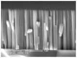
图1A和图1B分别为实施例3所述Cu-Cu2O核壳纳米线阵列膜表面和断面的SEM形貌图;FIG. 1A and FIG. 1B are SEM topographic images of the surface and cross-section of the Cu-Cu2 O core-shell nanowire array film described in Example 3, respectively;
图2A和图2B分别为实施例4所述Cu-Cu2O核壳纳米线阵列膜表面和断面的SEM形貌图;FIG. 2A and FIG. 2B are the SEM topographic images of the surface and the cross-section of the Cu-Cu2 O core-shell nanowire array film described in Example 4, respectively;
图3A和图3B分别为实施例2和实施例3所述Cu-Cu2O核壳纳米线阵列膜的TEM形貌图;FIG. 3A and FIG. 3B are TEM images of the Cu-Cu2 O core-shell nanowire array films described in Example 2 and Example 3, respectively;
图4为实施例3所述Cu-Cu2O核壳纳米线阵列膜电极的XPS分析图;4 is an XPS analysis diagram of the Cu-Cu2 O core-shell nanowire array membrane electrode described in Example 3;
图5为实施例3以及对比例2、对比例3所述膜电极的电导率对比图;5 is a comparison diagram of the electrical conductivity of the membrane electrodes described in Example 3, Comparative Example 2, and Comparative Example 3;
图6A和图6B分别为实施例3、实施例5、对比例2和对比例3所述膜经过-20℃至100℃范围内一千次冷热冲击后的表面自由能变化图和电阻变化图;6A and 6B are the surface free energy change diagram and resistance change of the films described in Example 3, Example 5, Comparative Example 2 and Comparative Example 3, respectively, after one thousand thermal shocks in the range of -20°C to 100°C picture;
图7A和图7B分别为实施例2、实施例3所述Cu-Cu2O核壳纳米线阵列膜以及玻璃衬底的热流密度与过热度关系图、换热系数与热流密度关系图。7A and 7B are the relationship between heat flux density and superheat degree, and the relationship map between heat transfer coefficient and heat flux density of the Cu-Cu2 O core-shell nanowire array film and the glass substrate described in Example 2 and Example 3, respectively.
具体实施方式Detailed ways
为使本发明的目的、技术方案和优点更加清楚,下面将对本发明的技术方案进行详细的描述。显然,所描述的实施例仅仅是本发明一部分实施例,而不是全部的实施例。基于本发明中的实施例,本领域普通技术人员在没有做出创造性劳动的前提下所得到的所有其它实施方式,都属于本发明所保护的范围。In order to make the objectives, technical solutions and advantages of the present invention clearer, the technical solutions of the present invention will be described in detail below. Obviously, the described embodiments are only some, but not all, embodiments of the present invention. Based on the embodiments of the present invention, all other implementations obtained by those of ordinary skill in the art without creative work fall within the protection scope of the present invention.
实施例1Example 1
本实施例提供一种具有抗氧化性能和增强散热功能的Cu-Cu2O核壳纳米线阵列膜电极的制备方法,包括如下步骤:This embodiment provides a method for preparing a Cu-Cu2 O core-shell nanowire array membrane electrode with anti-oxidation performance and enhanced heat dissipation, including the following steps:
(1)衬底预处理:(1) Substrate pretreatment:
将衬底硅片依次浸泡于洗洁精水(洗洁精与去离子水按照体积比1:5配制而成)、去离子水、无水乙醇、丙酮中进行超声清洗,用温度为20℃的高纯氮气将硅片吹干后,再对硅片进行等离子清洗,得到预处理后的硅片;Soak the substrate silicon wafer in detergent water (the volume ratio of detergent and deionized water is 1:5), deionized water, absolute ethanol, and acetone in turn for ultrasonic cleaning at a temperature of 20°C After drying the silicon wafer with high-purity nitrogen gas, the silicon wafer is plasma cleaned to obtain the pretreated silicon wafer;
(2)沉积Cu膜(2) Deposition of Cu film
利用直流磁控溅射方式在预处理后的硅片上沉积Cu膜,具体操作如下:The Cu film is deposited on the pretreated silicon wafer by DC magnetron sputtering. The specific operations are as follows:
(a)将Cu靶材放入磁控溅射仪的真空室中的直流台上,把衬底放置于样品台上,调节样品台与直流台的距离至90mm;样品台与直流台平面延长线的夹角为0度;(a) Put the Cu target on the DC stage in the vacuum chamber of the magnetron sputtering apparatus, place the substrate on the sample stage, and adjust the distance between the sample stage and the DC stage to 90 mm; the sample stage and the DC stage are extended in plane The included angle of the line is 0 degrees;
(b)对真空室抽真空,控制真空室内的真空度为2.0×10⁻⁴Pa;之后向真空室内充入氩气,充入氩气的流量为10sccm,调节氩气压强为0.5Pa;(b) evacuating the vacuum chamber, and controlling the vacuum degree in the vacuum chamber to be 2.0×10⁻⁴ Pa; then filling the vacuum chamber with argon gas, the flow rate of the filling argon gas is 10sccm, and the argon pressure is adjusted to 0.5Pa;
(c)施加直流电压(电流为80mA,电压为0.20kV)于紧接靶材的阴极和紧接基板后的阳极间,以在衬底上沉积Cu膜;进行所述沉积的温度为40℃,进行所述沉积的时间为1h,工作气压为0.5Pa,溅射功率设为16W;沉积Cu膜的厚度(纳米线的长度)为100-150nm,纳米线直径为50-100nm,纳米线阵列与衬底的夹角为90度;(c) applying a DC voltage (current of 80 mA, voltage of 0.20 kV) between the cathode immediately after the target and the anode immediately after the substrate to deposit a Cu film on the substrate; the temperature for the deposition was 40° C. , the deposition time is 1h, the working pressure is 0.5Pa, and the sputtering power is set to 16W; the thickness of the deposited Cu film (the length of the nanowires) is 100-150nm, the diameter of the nanowires is 50-100nm, and the nanowire array The included angle with the substrate is 90 degrees;
对所述Cu膜在控制真空室内的工作气压为0.5Pa,充入氩气的流量为30sccm,氧气的流量为1sccm,温度为100℃的有氧环境下进行原位退火处理15min,获得纳米线外层Cu2O膜的厚度为2nm,自然冷却后,即得所述Cu-Cu2O核壳纳米线阵列膜电极。The working pressure of the Cu film in the control vacuum chamber is 0.5 Pa, the flow rate of argon gas is 30 sccm, the flow rate of oxygen gas is 1 sccm, and the temperature is 100 ° C. Perform in-situ annealing treatment for 15 minutes in an aerobic environment to obtain nanowires. The thickness of the outer layer Cu2 O film is 2 nm, and after natural cooling, the Cu-Cu2 O core-shell nanowire array film electrode is obtained.
实施例2Example 2
本实施例提供一种Cu-Cu2O核壳纳米线阵列膜电极的制备方法,包括如下步骤:This embodiment provides a method for preparing a Cu-Cu2 O core-shell nanowire array membrane electrode, which includes the following steps:
(1)衬底预处理:(1) Substrate pretreatment:
将衬底玻璃依次浸泡于洗洁精水(洗洁精与去离子水按照体积比1:5配制而成)、去离子水、无水乙醇、丙酮中进行超声清洗,用温度为100℃的高纯氮气将玻璃吹干后,再对玻璃进行等离子清洗,得到预处理后的玻璃衬底;Soak the substrate glass in detergent water (the volume ratio of detergent and deionized water is 1:5), deionized water, absolute ethanol, and acetone in turn for ultrasonic cleaning. After the glass is blown dry by high-purity nitrogen, the glass is plasma cleaned to obtain a pretreated glass substrate;
(2)沉积Cu膜(2) Deposition of Cu film
利用直流磁控溅射方式在预处理后的硅片上沉积Cu膜,具体操作如下:The Cu film is deposited on the pretreated silicon wafer by DC magnetron sputtering. The specific operations are as follows:
(a)将Cu靶材放入磁控溅射仪的真空室中的直流台上,把衬底放置于样品台上,调节样品台与直流台的距离至50mm;样品台与直流台平面延长线的夹角为0度;(a) Put the Cu target on the DC stage in the vacuum chamber of the magnetron sputtering apparatus, place the substrate on the sample stage, and adjust the distance between the sample stage and the DC stage to 50mm; the plane of the sample stage and the DC stage is extended The included angle of the line is 0 degrees;
(b)对真空室抽真空,控制真空室内的真空度为4.0×10⁻⁴Pa;之后向真空室内充入氩气,充入氩气的流量为30sccm,调节氩气压强为1.5Pa;(b) evacuating the vacuum chamber, and controlling the vacuum degree in the vacuum chamber to be 4.0×10⁻⁴ Pa; then filling the vacuum chamber with argon gas, the flow rate of the argon gas filling is 30sccm, and the argon pressure is adjusted to 1.5Pa;
(c)施加直流电压(电流为120mA,电压为0.20kV)于紧接靶材的阴极和紧接基板后的阳极间,以在衬底上沉积Cu膜;进行所述沉积的温度为40℃,进行所述沉积的时间为15h,工作气压为1.5Pa,溅射功率设为24W;沉积Cu膜的厚度(纳米线的长度)为16350nm,纳米线直径为280-350nm,纳米线阵列与衬底的夹角为90度;(c) applying a DC voltage (current is 120 mA, voltage is 0.20 kV) between the cathode immediately after the target and the anode immediately after the substrate to deposit a Cu film on the substrate; the temperature for the deposition is 40° C. , the deposition time is 15h, the working pressure is 1.5Pa, and the sputtering power is set to 24W; the thickness of the deposited Cu film (the length of the nanowire) is 16350nm, the diameter of the nanowire is 280-350nm, and the nanowire array and the lining The included angle of the bottom is 90 degrees;
对所述Cu膜在控制真空室内的工作气压为1.5Pa,充入氩气的流量为10sccm,氧气的流量为10sccm,温度为200℃的有氧环境下进行原位退火处理25min,获得纳米线外层Cu2O膜的厚度为20nm,自然冷却后,即得所述Cu-Cu2O核壳纳米线阵列膜电极。The working pressure of the Cu film in the control vacuum chamber is 1.5Pa, the flow rate of argon gas is 10sccm, the flow rate of oxygen gas is 10sccm, and the temperature is 200 ℃ in an aerobic environment to perform in-situ annealing treatment for 25min to obtain nanowires The thickness of the outer layer Cu2 O film is 20 nm, and after natural cooling, the Cu-Cu2 O core-shell nanowire array film electrode is obtained.
实施例3Example 3
本实施例提供一种Cu-Cu2O核壳纳米线阵列膜电极的制备方法,包括如下步骤:This embodiment provides a method for preparing a Cu-Cu2 O core-shell nanowire array membrane electrode, which includes the following steps:
(1)衬底预处理:(1) Substrate pretreatment:
将衬底石英依次浸泡于洗洁精水(洗洁精与去离子水按照体积比1:5配制而成)、去离子水、无水乙醇、丙酮中进行超声清洗,用温度为40℃的高纯氮气将石英吹干后,再对石英进行等离子清洗,得到预处理后的石英衬底;The substrate quartz was immersed in detergent water (the volume ratio of detergent and deionized water was 1:5), deionized water, absolute ethanol, and acetone in turn for ultrasonic cleaning, and the temperature was 40 ℃. After drying the quartz with high-purity nitrogen, the quartz is plasma cleaned to obtain a pretreated quartz substrate;
(2)沉积Cu膜(2) Deposition of Cu film
利用直流磁控溅射方式在预处理后的硅片上沉积Cu膜,具体操作如下:The Cu film is deposited on the pretreated silicon wafer by DC magnetron sputtering. The specific operations are as follows:
(a)将Cu靶材放入磁控溅射仪的真空室中的直流台上,把衬底放置于样品台上,调节样品台与直流台的距离至50mm;样品台与直流台平面延长线的夹角为0度;(a) Put the Cu target on the DC stage in the vacuum chamber of the magnetron sputtering apparatus, place the substrate on the sample stage, and adjust the distance between the sample stage and the DC stage to 50mm; the plane of the sample stage and the DC stage is extended The included angle of the line is 0 degrees;
(b)对真空室抽真空,控制真空室内的真空度为4.0×10⁻⁴Pa;之后向真空室内充入氩气,充入氩气的流量为30sccm,调节氩气压强为1.0Pa;(b) evacuating the vacuum chamber, and controlling the vacuum degree in the vacuum chamber to be 4.0×10⁻⁴ Pa; then filling the vacuum chamber with argon gas, the flow rate of the filling argon gas is 30sccm, and the argon pressure is adjusted to 1.0Pa;
(c)施加直流电压(电流为80mA,电压为0.35kV)于紧接靶材的阴极和紧接基板后的阳极间,以在衬底上沉积Cu膜;进行所述沉积的温度为40℃,进行所述沉积的时间为3h,工作气压为1.0Pa,溅射功率设为28W;沉积Cu膜的厚度(纳米线的长度)为3200-3300nm,纳米线直径为250-300nm,纳米线阵列与衬底的夹角为90度;(c) applying a DC voltage (current of 80 mA, voltage of 0.35 kV) between the cathode immediately after the target and the anode immediately after the substrate to deposit a Cu film on the substrate; the temperature for the deposition was 40° C. , the deposition time is 3h, the working pressure is 1.0Pa, and the sputtering power is set to 28W; the thickness of the deposited Cu film (the length of the nanowires) is 3200-3300nm, the diameter of the nanowires is 250-300nm, and the nanowire array The included angle with the substrate is 90 degrees;
对所述Cu膜在控制真空室内的工作气压为1.5Pa,充入氩气的流量为30sccm,氧气的流量为5sccm,温度为200℃的有氧环境下进行原位退火处理25min,外层Cu2O膜的厚度为10-15nm,自然冷却后,即得所述Cu-Cu2O核壳纳米线阵列膜电极。The working pressure of the Cu film in the control vacuum chamber is 1.5Pa, the flow rate of argon gas is 30sccm, the flow rate of oxygen gas is 5sccm, and the temperature is 200 ° C. Under the aerobic environment, in-situ annealing treatment is carried out for 25min, and the outer layer Cu The thickness of the2 O film is 10-15 nm, and after natural cooling, the Cu-Cu2 O core-shell nanowire array membrane electrode is obtained.
实施例4Example 4
本实施例提供一种Cu-Cu2O核壳纳米线阵列膜电极的制备方法,包括如下步骤:This embodiment provides a method for preparing a Cu-Cu2 O core-shell nanowire array membrane electrode, which includes the following steps:
(1)衬底预处理:(1) Substrate pretreatment:
将聚酰亚胺衬底依次浸泡于洗洁精水(洗洁精与去离子水按照体积比1:5配制而成)、去离子水、无水乙醇、丙酮中进行超声清洗,用温度为100℃的高纯氮气将聚酰亚胺衬底吹干后,再对聚酰亚胺衬底进行等离子清洗,得到预处理后的聚酰亚胺衬底;The polyimide substrate was immersed in detergent water (the volume ratio of detergent and deionized water was 1:5), deionized water, absolute ethanol, and acetone in turn for ultrasonic cleaning, and the temperature was After the polyimide substrate is blown dry by high-purity nitrogen gas at 100°C, the polyimide substrate is plasma cleaned to obtain a pretreated polyimide substrate;
(2)沉积Cu膜(2) Deposition of Cu film
利用直流磁控溅射方式在预处理后的硅片上沉积Cu膜,具体操作如下:The Cu film is deposited on the pretreated silicon wafer by DC magnetron sputtering. The specific operations are as follows:
(a)将Cu靶材放入磁控溅射仪的真空室中的直流台上,把衬底放置于样品台上,调节样品台与直流台的距离至50mm;样品台与直流台平面延长线的夹角为45度;(a) Put the Cu target on the DC stage in the vacuum chamber of the magnetron sputtering apparatus, place the substrate on the sample stage, and adjust the distance between the sample stage and the DC stage to 50mm; the plane of the sample stage and the DC stage is extended The included angle of the lines is 45 degrees;
(b)对真空室抽真空,控制真空室内的真空度为4.0×10⁻⁴Pa;之后向真空室内充入氩气,充入氩气的流量为30sccm,调节氩气压强为0.5Pa;(b) evacuating the vacuum chamber, and controlling the vacuum degree in the vacuum chamber to be 4.0×10⁻⁴ Pa; then filling the vacuum chamber with argon gas, the flow rate of the filling argon gas is 30sccm, and the argon pressure is adjusted to 0.5Pa;
(c)施加直流电压(电流为100mA,电压为0.30kV)于紧接靶材的阴极和紧接基板后的阳极间,以在衬底上沉积Cu膜;进行所述沉积的温度为40℃,进行所述沉积的时间为4h,工作气压为1.0Pa,溅射功率设为30W;沉积Cu膜的厚度(纳米线的长度)为3400-3500nm,纳米线直径为250-350nm,纳米线阵列与衬底的夹角为80度;(c) applying a DC voltage (current is 100 mA, voltage is 0.30 kV) between the cathode immediately after the target and the anode immediately after the substrate to deposit a Cu film on the substrate; the temperature for the deposition is 40° C. , the deposition time is 4h, the working pressure is 1.0Pa, and the sputtering power is set to 30W; the thickness of the deposited Cu film (the length of the nanowire) is 3400-3500nm, the diameter of the nanowire is 250-350nm, and the nanowire array The included angle with the substrate is 80 degrees;
对所述Cu膜在控制真空室内的工作气压为1.5Pa,充入氩气的流量为30sccm,氧气的流量为5sccm,温度为200℃的有氧环境下进行原位退火处理25min,外层Cu2O膜的厚度为10-15nm,自然冷却后,即得所述Cu-Cu2O核壳纳米线阵列膜电极。The working pressure of the Cu film in the control vacuum chamber is 1.5Pa, the flow rate of argon gas is 30sccm, the flow rate of oxygen gas is 5sccm, and the temperature is 200 ° C. Under the aerobic environment, in-situ annealing treatment is carried out for 25min, and the outer layer Cu The thickness of the2 O film is 10-15 nm, and after natural cooling, the Cu-Cu2 O core-shell nanowire array membrane electrode is obtained.
实施例5Example 5
本实施例提供一种Cu-Cu2O核壳纳米线阵列膜电极的制备方法,包括如下步骤:This embodiment provides a method for preparing a Cu-Cu2 O core-shell nanowire array membrane electrode, which includes the following steps:
(1)衬底预处理:(1) Substrate pretreatment:
将氮化铝衬底依次浸泡于洗洁精水(洗洁精与去离子水按照体积比1:5配制而成)、去离子水、无水乙醇、丙酮中进行超声清洗,用温度为100℃的高纯氮气将氮化铝衬底吹干后,再对氮化铝衬底进行等离子清洗,得到预处理后的氮化铝衬底;The aluminum nitride substrate was immersed in detergent water (the volume ratio of detergent and deionized water was 1:5), deionized water, absolute ethanol, and acetone in turn for ultrasonic cleaning, and the temperature was 100 °C. After drying the aluminum nitride substrate with high-purity nitrogen at ℃, the aluminum nitride substrate is plasma cleaned to obtain the pretreated aluminum nitride substrate;
(2)沉积Cu膜(2) Deposition of Cu film
利用直流磁控溅射方式在预处理后的硅片上沉积Cu膜,具体操作如下:The Cu film is deposited on the pretreated silicon wafer by DC magnetron sputtering. The specific operations are as follows:
(a)将Cu靶材放入磁控溅射仪的真空室中的直流台上,把衬底放置于样品台上,调节样品台与直流台的距离至90mm;样品台与直流台平面延长线的夹角为45度;(a) Put the Cu target on the DC stage in the vacuum chamber of the magnetron sputtering apparatus, place the substrate on the sample stage, and adjust the distance between the sample stage and the DC stage to 90 mm; the sample stage and the DC stage are extended in plane The included angle of the lines is 45 degrees;
(b)对真空室抽真空,控制真空室内的真空度为4.0×10⁻⁴Pa;之后向真空室内充入氩气,充入氩气的流量为30sccm,调节氩气压强为0.5Pa;(b) evacuating the vacuum chamber, and controlling the vacuum degree in the vacuum chamber to be 4.0×10⁻⁴ Pa; then filling the vacuum chamber with argon gas, the flow rate of the filling argon gas is 30sccm, and the argon pressure is adjusted to 0.5Pa;
(c)施加直流电压(电流为100mA,电压为0.30kV)于紧接靶材的阴极和紧接基板后的阳极间,以在衬底上沉积Cu膜;进行所述沉积的温度为180℃,进行所述沉积的时间为3h,工作气压为0.5Pa,溅射功率设为30W;沉积Cu膜的厚度(纳米线的长度)为750-850nm,纳米线直径为50-100nm,纳米线阵列与衬底的夹角为90度;(c) applying a DC voltage (current is 100 mA, voltage is 0.30 kV) between the cathode immediately after the target and the anode immediately after the substrate to deposit a Cu film on the substrate; the temperature for the deposition is 180° C. , the deposition time is 3h, the working pressure is 0.5Pa, and the sputtering power is set to 30W; the thickness of the deposited Cu film (the length of the nanowire) is 750-850nm, the diameter of the nanowire is 50-100nm, and the nanowire array The included angle with the substrate is 90 degrees;
对所述Cu膜在控制真空室内的工作气压为1.5Pa,充入氩气的流量为30sccm,氧气的流量为1sccm,温度为200℃的有氧环境下进行原位退火处理25min,外层Cu2O膜的厚度为5-8nm,自然冷却后,即得所述Cu-Cu2O核壳纳米线阵列膜电极。The working pressure of the Cu film in the control vacuum chamber is 1.5Pa, the flow rate of argon gas is 30sccm, the flow rate of oxygen gas is 1sccm, and the temperature is 200 ° C. Under the aerobic environment, in-situ annealing treatment is performed for 25min, and the outer layer Cu The thickness of the2 O film is 5-8 nm, and after natural cooling, the Cu-Cu2 O core-shell nanowire array membrane electrode is obtained.
对比例1Comparative Example 1
本对比例提供一种Cu纳米线阵列膜电极,与实施例1的区别仅在于:步骤(3)的退火处理在真空条件下进行,且退火温度不同,具体为:This comparative example provides a Cu nanowire array membrane electrode, which is different from Example 1 only in that the annealing treatment in step (3) is performed under vacuum conditions, and the annealing temperature is different, specifically:
对所述Cu膜在真空度为2.0×10⁻⁴Pa的环境下进行室温条件下原位退火处理,自然冷却后,制得Cu纳米线阵列膜电极。The Cu film is annealed in-situ at room temperature in an environment with a vacuum degree of 2.0×10⁻⁴ Pa, and after natural cooling, a Cu nanowire array film electrode is prepared.
对比例2Comparative Example 2
本对比例提供一种Cu纳米线阵列膜电极,与实施例1的区别仅在于:步骤(3)的退火处理在真空条件下进行,且退火温度不同,具体为:This comparative example provides a Cu nanowire array membrane electrode, which is different from Example 1 only in that the annealing treatment in step (3) is performed under vacuum conditions, and the annealing temperature is different, specifically:
对所述Cu膜在真空度为2.0×10⁻⁴Pa的环境下进行200℃条件下原位退火处理,自然冷却后,制得Cu纳米线阵列半连续薄膜电极。The Cu film is annealed in-situ at 200° C. in an environment with a vacuum degree of 2.0×10⁻⁴ Pa, and after natural cooling, a Cu nanowire array semi-continuous thin film electrode is prepared.
对比例3Comparative Example 3
本对比例提供一种Cu-CuxO核壳薄膜电极,与实施例1的区别仅在于:步骤(2)中沉积温度为300℃,制得Cu-CuxO(1<x<2,CuO和Cu2O的复合物)核壳薄膜电极中Cu膜呈连续膜的形态。This comparative example provides a Cu-Cux O core-shell thin film electrode, which differs from Example 1 only in that the deposition temperature in step (2) is 300°C, and Cu-Cux O (1<x<2, The composite of CuO and Cu2 O) Cu film in the core-shell thin film electrode is in the form of continuous film.
实验例Experimental example
对实施例2-5、对比例2-3所得膜材料进行形貌和性能检测,具体如下。The morphology and performance of the membrane materials obtained in Examples 2-5 and Comparative Examples 2-3 were tested, as follows.
如图1A和图1B所示分别为实施例3所述Cu-Cu2O核壳纳米线阵列膜的表面和断面的SEM形貌图,从图中可以看出膜厚度为3.25微米,纳米线的直径约为100nm,纳米线阵列与衬底的夹角为90度,说明采用该条件可以制备出具有纳米线阵列结构的膜材料。1A and 1B are the SEM images of the surface and cross-section of the Cu-Cu2 O core-shell nanowire array film described in Example 3, respectively. It can be seen from the figures that the film thickness is 3.25 microns, and the nanowires The diameter of the nanowire array is about 100 nm, and the angle between the nanowire array and the substrate is 90 degrees, which shows that the film material with the nanowire array structure can be prepared under this condition.
如图2A和图2B所示分别为实施例4所述具有倾斜结构Cu-Cu2O核壳纳米线阵列膜的表面和断面的SEM形貌图,从图中可以看出膜厚度为3.45微米,纳米线的直径约为230nm,纳米线阵列与衬底的夹角为80度,说明采用该条件可以制备出具有倾斜结构的纳米线阵列膜材料。Figures 2A and 2B are the SEM images of the surface and the cross-section of the Cu-Cu2 O core-shell nanowire array film with an inclined structure described in Example 4, respectively. It can be seen from the figures that the film thickness is 3.45 microns , the diameter of the nanowires is about 230nm, and the angle between the nanowire array and the substrate is 80 degrees, indicating that the nanowire array film material with inclined structure can be prepared under this condition.
如图3A和图3B所示分别为实施例2和实施例3所述Cu-Cu2O核壳纳米线阵列膜的TEM形貌图,从图中可以看出纳米线外层包覆着一层无定形状态的Cu2O膜,膜厚度约为18nm,膜中不均匀分散着Cu纳米颗粒,说明采用该实验参数可以制备出具有核壳结构的铜纳米线阵列膜。Figures 3A and 3B are the TEM images of the Cu-Cu2 O core-shell nanowire array films described in Example 2 and Example 3, respectively. It can be seen from the figures that the outer layer of the nanowires is covered with a An amorphous Cu2 O film with a film thickness of about 18 nm and Cu nanoparticles dispersed unevenly in the film indicates that the copper nanowire array film with core-shell structure can be prepared by using the experimental parameters.
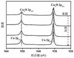
如图4所示为实施例3所述Cu-Cu2O核壳纳米线阵列膜电极的XPS分析图,从图中可以看出Cu-Cu2O核壳纳米线的表层为Cu2O,随着刻蚀深度加深,内部逐渐转化为Cu,进一步确证采用该实验参数可以制备出具有核壳结构的Cu-Cu2O核壳纳米线。Figure 4 shows the XPS analysis diagram of the Cu-Cu2 O core-shell nanowire array membrane electrode described in Example 3. It can be seen from the figure that the surface layer of the Cu-Cu2 O core-shell nanowire is Cu2 O, With the deepening of the etching depth, the interior is gradually converted into Cu, which further confirms that Cu-Cu2 O core-shell nanowires with core-shell structure can be prepared by using the experimental parameters.
如图5所示为实施例3以及对比例2、对比例3所述膜电极的电导率,从图中可以看出对比例3所得“连续薄膜”的电导率随着温度的升高逐渐降低,呈现典型的金属特性;对比例2所得“半连续薄膜”和实施例3所得的“纳米线阵列膜”的电导率呈现S形变化趋势,随着温度的升高电导率先降低后升高,最后逐渐稳定。Figure 5 shows the electrical conductivity of the membrane electrodes in Example 3, Comparative Example 2, and Comparative Example 3. It can be seen from the figure that the electrical conductivity of the "continuous thin film" obtained in Comparative Example 3 gradually decreases with the increase of temperature. , showing typical metallic properties; the electrical conductivity of the "semi-continuous film" obtained in Comparative Example 2 and the "nanowire array film" obtained in Example 3 showed a S-shaped trend, and the conductivity first decreased and then increased with the increase of temperature. finally stabilized.
如图6A所示为实施例3、实施例5、对比例2和对比例3所述膜经过-20至100℃范围内一千次冷热冲击后的表面自由能变化图,图6B所示为实施例3、实施例5、对比例2和对比例3所述膜经过-20至100℃范围内一千次冷热冲击后的电阻率变化图,从图中可以看出“具有核壳结构的纳米线阵列膜”具有稳定的表面状态和电阻值,说明采用该条件制备的纳米线阵列膜具有很好的抗氧化性能和自我保护性能。Figure 6A shows the surface free energy changes of the films of Example 3, Example 5, Comparative Example 2 and Comparative Example 3 after one thousand thermal shocks in the range of -20 to 100°C, and Figure 6B For example 3, example 5, comparative example 2 and comparative example 3, the resistivity change diagram of the films after one thousand times of thermal shocks in the range of -20 to 100 °C, it can be seen from the figure that "with core-shell" The structured nanowire array film" has stable surface state and resistance value, indicating that the nanowire array film prepared under this condition has good anti-oxidation performance and self-protection performance.
如图7A和图7B所示分别为实施例2、实施例3所述膜以及未修饰平面(衬底玻璃)的热流密度与过热度关系图、换热系数与热流密度关系图,从图中可以看出Cu-Cu2O核壳纳米线阵列膜可以有效增强铜柱表面的换热性能,说明采用Cu-Cu2O核壳纳米线阵列膜作为电极材料进行应用,可以有效改善电极材料的散热性能,是一种新型的电极材料。As shown in FIG. 7A and FIG. 7B are the relationship diagrams of heat flux and superheat degree, heat transfer coefficient and heat flux density of the films described in Example 2 and Example 3 and the unmodified plane (substrate glass), respectively. It can be seen that the Cu-Cu2 O core-shell nanowire array film can effectively enhance the heat transfer performance of the surface of the copper column, indicating that the application of the Cu-Cu2 O core-shell nanowire array film as the electrode material can effectively improve the performance of the electrode material. Heat dissipation performance, is a new type of electrode material.
以上所述,仅为本发明的具体实施方式,但本发明的保护范围并不局限于此,任何熟悉本技术领域的技术人员在本发明揭露的技术范围内,可轻易想到变化或替换,都应涵盖在本发明的保护范围之内。因此,本发明的保护范围应以所述权利要求的保护范围为准。The above are only specific embodiments of the present invention, but the protection scope of the present invention is not limited to this. Any person skilled in the art can easily think of changes or substitutions within the technical scope disclosed by the present invention. should be included within the protection scope of the present invention. Therefore, the protection scope of the present invention should be based on the protection scope of the claims.
Claims (10)
Priority Applications (1)
| Application Number | Priority Date | Filing Date | Title |
|---|---|---|---|
| CN201910958729.2ACN110668392B (en) | 2019-10-10 | 2019-10-10 | Enhanced heat dissipation Cu-Cu 2 O-core-shell nanowire array self-protection electrode and preparation method thereof |
Applications Claiming Priority (1)
| Application Number | Priority Date | Filing Date | Title |
|---|---|---|---|
| CN201910958729.2ACN110668392B (en) | 2019-10-10 | 2019-10-10 | Enhanced heat dissipation Cu-Cu 2 O-core-shell nanowire array self-protection electrode and preparation method thereof |
Publications (2)
| Publication Number | Publication Date |
|---|---|
| CN110668392Atrue CN110668392A (en) | 2020-01-10 |
| CN110668392B CN110668392B (en) | 2023-03-14 |
Family
ID=69081507
Family Applications (1)
| Application Number | Title | Priority Date | Filing Date |
|---|---|---|---|
| CN201910958729.2AActiveCN110668392B (en) | 2019-10-10 | 2019-10-10 | Enhanced heat dissipation Cu-Cu 2 O-core-shell nanowire array self-protection electrode and preparation method thereof |
Country Status (1)
| Country | Link |
|---|---|
| CN (1) | CN110668392B (en) |
Cited By (1)
| Publication number | Priority date | Publication date | Assignee | Title |
|---|---|---|---|---|
| CN111293324A (en)* | 2020-03-24 | 2020-06-16 | 成都新柯力化工科技有限公司 | Anti-oxidation gas diffusion layer of fuel cell and preparation method thereof |
Citations (8)
| Publication number | Priority date | Publication date | Assignee | Title |
|---|---|---|---|---|
| JP2007246993A (en)* | 2006-03-16 | 2007-09-27 | Saitama Univ | Method for forming copper oxide thin film |
| CN102181831A (en)* | 2011-04-15 | 2011-09-14 | 河南大学 | Preparation method for copper oxide nano line array film |
| CN102623521A (en)* | 2011-01-31 | 2012-08-01 | 中国科学院物理研究所 | A kind of preparation method of cuprous oxide film |
| US20130143402A1 (en)* | 2010-08-20 | 2013-06-06 | Nanmat Technology Co., Ltd. | Method of forming Cu thin film |
| CN103341624A (en)* | 2013-07-16 | 2013-10-09 | 南开大学 | A method for preparing Cu-Cu2O core-shell ferromagnetic nanoparticles |
| CN103510048A (en)* | 2013-08-19 | 2014-01-15 | 南京清航新材料科技有限公司 | Preparation method of copper nanowire arrays with porous structure and film conductivity measuring method thereof |
| CN105621474A (en)* | 2015-12-29 | 2016-06-01 | 中国石油化工股份有限公司 | Hyperbranched graded cuprous oxide nanomateiral and preparation method and application thereof |
| CN107505366A (en)* | 2017-09-22 | 2017-12-22 | 合肥工业大学 | A kind of preparation of Cu oxide core-shell nano linear array material and purposes |
- 2019
- 2019-10-10CNCN201910958729.2Apatent/CN110668392B/enactiveActive
Patent Citations (8)
| Publication number | Priority date | Publication date | Assignee | Title |
|---|---|---|---|---|
| JP2007246993A (en)* | 2006-03-16 | 2007-09-27 | Saitama Univ | Method for forming copper oxide thin film |
| US20130143402A1 (en)* | 2010-08-20 | 2013-06-06 | Nanmat Technology Co., Ltd. | Method of forming Cu thin film |
| CN102623521A (en)* | 2011-01-31 | 2012-08-01 | 中国科学院物理研究所 | A kind of preparation method of cuprous oxide film |
| CN102181831A (en)* | 2011-04-15 | 2011-09-14 | 河南大学 | Preparation method for copper oxide nano line array film |
| CN103341624A (en)* | 2013-07-16 | 2013-10-09 | 南开大学 | A method for preparing Cu-Cu2O core-shell ferromagnetic nanoparticles |
| CN103510048A (en)* | 2013-08-19 | 2014-01-15 | 南京清航新材料科技有限公司 | Preparation method of copper nanowire arrays with porous structure and film conductivity measuring method thereof |
| CN105621474A (en)* | 2015-12-29 | 2016-06-01 | 中国石油化工股份有限公司 | Hyperbranched graded cuprous oxide nanomateiral and preparation method and application thereof |
| CN107505366A (en)* | 2017-09-22 | 2017-12-22 | 合肥工业大学 | A kind of preparation of Cu oxide core-shell nano linear array material and purposes |
Non-Patent Citations (1)
| Title |
|---|
| YU-MIN SHEN等: ""Characterization of ordered Cu2O nanowire arrays prepared by heat treated Cu/PAM composite"", 《THIN SOLID FILMS》* |
Cited By (1)
| Publication number | Priority date | Publication date | Assignee | Title |
|---|---|---|---|---|
| CN111293324A (en)* | 2020-03-24 | 2020-06-16 | 成都新柯力化工科技有限公司 | Anti-oxidation gas diffusion layer of fuel cell and preparation method thereof |
Also Published As
| Publication number | Publication date |
|---|---|
| CN110668392B (en) | 2023-03-14 |
Similar Documents
| Publication | Publication Date | Title |
|---|---|---|
| US7811149B2 (en) | Method for fabricating carbon nanotube-based field emission device | |
| CN108172488A (en) | Carbon nanometer field-transmitting cathode and its manufacturing method and application | |
| CN108821331B (en) | A kind of preparation method and product of gallium oxide nanorod | |
| CN104851765B (en) | Method for improving field emission performance of carbon nano tube by microwave hydrogen plasma treatment | |
| CN108231507A (en) | A kind of photocathode based on novel nano structure and preparation method thereof | |
| CN101086940A (en) | Making method of field radiation cathode device | |
| JP2007123280A (en) | Carbon nanotubes with ZnO protrusions | |
| JP3792977B2 (en) | Electron emission film and field emission cold cathode device | |
| CN114959697A (en) | Preparation method of graphene/copper composite material combining physical vapor deposition and chemical vapor deposition | |
| CN103769025A (en) | Microbubble generator and preparation method thereof | |
| CN110668392B (en) | Enhanced heat dissipation Cu-Cu 2 O-core-shell nanowire array self-protection electrode and preparation method thereof | |
| CN106098503B (en) | A kind of graphene ribbon-like electron note field emission cold-cathode and its production method | |
| CN105118821A (en) | On-chip inductor based on graphene/metal composite wire and preparation method | |
| CN105513921B (en) | Carbon nanometer field-transmitting cathode and its preparation method and application | |
| CN104882346B (en) | A preparation method of carbon nanotube array field emission cathode coated with carbon nanoparticles | |
| CN102107854A (en) | Method for manufacturing multi-walled carbon nanotube electrode | |
| CN117393403A (en) | A kind of carbon nanotube field emission cathode and preparation method thereof | |
| CN117393402A (en) | A kind of carbon nanotube field emission cathode and preparation method thereof | |
| CN112582184A (en) | Nanowire electrode, capacitor electrode and preparation method of nanowire electrode and capacitor electrode | |
| CN101280415A (en) | A method for nickel-plating the surface of silicon nanowires | |
| CN108987218B (en) | A method to improve the field emission performance of graphene sheet-silicon nanowire array composite material | |
| CN103811240B (en) | Carbon nano-tube cathode preparation method | |
| JP4086803B2 (en) | Method for manufacturing flexible printed circuit board | |
| CN116162915A (en) | Antistatic adhesive tape with coating layer | |
| EP1251543A1 (en) | Vacuum power switches |
Legal Events
| Date | Code | Title | Description |
|---|---|---|---|
| PB01 | Publication | ||
| PB01 | Publication | ||
| SE01 | Entry into force of request for substantive examination | ||
| SE01 | Entry into force of request for substantive examination | ||
| GR01 | Patent grant | ||
| GR01 | Patent grant |