CN110664379A - A device for collecting images of human head skin - Google Patents
A device for collecting images of human head skinDownload PDFInfo
- Publication number
- CN110664379A CN110664379ACN201911075940.6ACN201911075940ACN110664379ACN 110664379 ACN110664379 ACN 110664379ACN 201911075940 ACN201911075940 ACN 201911075940ACN 110664379 ACN110664379 ACN 110664379A
- Authority
- CN
- China
- Prior art keywords
- unit
- pin
- led
- main control
- resistor
- Prior art date
- Legal status (The legal status is an assumption and is not a legal conclusion. Google has not performed a legal analysis and makes no representation as to the accuracy of the status listed.)
- Pending
Links
Images


Classifications
- A—HUMAN NECESSITIES
- A61—MEDICAL OR VETERINARY SCIENCE; HYGIENE
- A61B—DIAGNOSIS; SURGERY; IDENTIFICATION
- A61B5/00—Measuring for diagnostic purposes; Identification of persons
- A61B5/0059—Measuring for diagnostic purposes; Identification of persons using light, e.g. diagnosis by transillumination, diascopy, fluorescence
- A61B5/0077—Devices for viewing the surface of the body, e.g. camera, magnifying lens
- A—HUMAN NECESSITIES
- A61—MEDICAL OR VETERINARY SCIENCE; HYGIENE
- A61B—DIAGNOSIS; SURGERY; IDENTIFICATION
- A61B5/00—Measuring for diagnostic purposes; Identification of persons
- A61B5/44—Detecting, measuring or recording for evaluating the integumentary system, e.g. skin, hair or nails
- A61B5/441—Skin evaluation, e.g. for skin disorder diagnosis
- A61B5/446—Scalp evaluation or scalp disorder diagnosis, e.g. dandruff
- H—ELECTRICITY
- H04—ELECTRIC COMMUNICATION TECHNIQUE
- H04N—PICTORIAL COMMUNICATION, e.g. TELEVISION
- H04N23/00—Cameras or camera modules comprising electronic image sensors; Control thereof
- H04N23/60—Control of cameras or camera modules
- H04N23/67—Focus control based on electronic image sensor signals
Landscapes
- Health & Medical Sciences (AREA)
- Life Sciences & Earth Sciences (AREA)
- Engineering & Computer Science (AREA)
- Medical Informatics (AREA)
- Surgery (AREA)
- Biophysics (AREA)
- Biomedical Technology (AREA)
- Heart & Thoracic Surgery (AREA)
- Physics & Mathematics (AREA)
- Molecular Biology (AREA)
- Pathology (AREA)
- Animal Behavior & Ethology (AREA)
- General Health & Medical Sciences (AREA)
- Public Health (AREA)
- Veterinary Medicine (AREA)
- Dermatology (AREA)
- Multimedia (AREA)
- Signal Processing (AREA)
- Circuit Arrangement For Electric Light Sources In General (AREA)
Abstract
Translated fromChinese
Description
Translated fromChinese技术领域technical field
本发明涉及图像检测和分析技术领域,特别是一种采集人体头部皮肤图像的装置。The invention relates to the technical field of image detection and analysis, in particular to a device for collecting human head skin images.
背景技术Background technique
目前,毛发作为一种常用的皮肤辅助器,是机体健康的重要外表标志之一。专业的头皮检测仪可以帮助大家直观快速地了解自己的头发情形和秃头状况,及时了解自己头发毛囊的健康状态,预防和阻止秃头发生。传统头部皮肤检测摄像头,获取头部皮肤图像需要手动调焦,操作麻烦;可视区域少,只能局部检查,不能全面反映人体头部整体的毛发生长情况。At present, hair, as a commonly used skin aid, is one of the important appearance indicators of the body's health. A professional scalp detector can help you understand your hair and baldness intuitively and quickly, understand the health of your hair follicles in time, and prevent and prevent baldness. The traditional head skin detection camera requires manual focus adjustment to obtain the head skin image, which is troublesome to operate; the visible area is small, and it can only be checked locally, and cannot fully reflect the overall hair growth of the human head.
发明内容SUMMARY OF THE INVENTION
本发明要解决的技术问题是针对上述现有技术的不足,提供一种采集人体头部皮肤图像的装置,采用自动调焦方式取代传统的手动调焦方式,降低用户获取头部皮肤图像的复杂度,扩大检测的可视区域,方便检测系统对头部皮肤的整体状态做分析。The technical problem to be solved by the present invention is to aim at the above-mentioned shortcomings of the prior art, and provide a device for collecting human head skin images, which adopts an automatic focusing method to replace the traditional manual focusing method, and reduces the complexity of obtaining the head skin images for users. It can expand the visual area of detection, and it is convenient for the detection system to analyze the overall state of the head skin.
为解决上述技术问题,本发明所采取的技术方案是:一种采集人体头部皮肤图像的装置,其包括电机驱动单元、LED驱动单元、主控单元、摄像头单元、HUB集线器单元和上位机;所述电机驱动单元用于驱动步进电机,步进电机带动摄像头前进后退实现自动对焦;所述LED驱动单元用于控制LED光源熄灭或者点亮状态,为摄像头提供光源;所述主控单元与LED驱动单元和电机驱动单元通信连接,用于控制电机运动和LED光源的状态,并且主控单元通过HUB集线器单元连接到上位机,与上位机进行数据交互;所述摄像头单元用于采集图像,通过HUB集线器单元连接到上位机,把图像传输到上位机;所述HUB集线器单元将主控单元和摄像头单元通过USB总线连接到上位机;所述上位机通过HUB集线器单元采集摄像头单元的图像,并且通过HUB集线器单元连接主控单元,从而控制步进电机和LED光源。In order to solve the above-mentioned technical problems, the technical scheme adopted by the present invention is: a device for collecting human head skin images, which includes a motor drive unit, an LED drive unit, a main control unit, a camera unit, a HUB hub unit and a host computer; The motor drive unit is used to drive a stepping motor, which drives the camera forward and backward to realize automatic focusing; the LED drive unit is used to control the LED light source to be turned off or on, and provide a light source for the camera; the main control unit is connected to the camera. The LED drive unit and the motor drive unit are connected in communication to control the motion of the motor and the state of the LED light source, and the main control unit is connected to the host computer through the HUB hub unit to exchange data with the host computer; the camera unit is used to collect images, The HUB hub unit is connected to the upper computer, and the image is transmitted to the upper computer; the HUB hub unit connects the main control unit and the camera unit to the upper computer through the USB bus; the upper computer collects the image of the camera unit through the HUB hub unit, And connect the main control unit through the HUB hub unit to control the stepper motor and the LED light source.
上述技术方案中,所述电机驱动单元包括电机驱动芯片U1、U2、降压芯片U4以及端子P1、P2、P3,U1用于控制实现摄像头变焦功能的步进电机A,U2用于控制实现摄像头聚焦功能的步进电机B,U4用于将5V降为3.3V,端子P1用于选择U1、U2的电源为5V或3.3V,通过端子P2连接到主控单元的I/O引脚,通过端子P3连接到步进电机A、B。所述电机驱动芯片U1、U2的芯片型号为L293DD。In the above technical solution, the motor drive unit includes motor drive chips U1, U2, step-down chip U4 and terminals P1, P2, P3, U1 is used to control the stepping motor A that realizes the zoom function of the camera, and U2 is used to control the realization of the camera. Stepping motor B with focusing function, U4 is used to reduce 5V to 3.3V, terminal P1 is used to select the power supply of U1 and U2 to 5V or 3.3V, and is connected to the I/O pin of the main control unit through terminal P2. Terminal P3 is connected to stepper motors A, B. The chip model of the motor drive chips U1 and U2 is L293DD.
上述技术方案中,所述LED驱动单元包括LED驱动芯片U1、U2、U3;U1的EN引脚通过电阻R1下拉到GND,默认使U1处于关闭状态,LED熄灭;EN连接到电阻R7,电阻R7的另一端连接到控制信号R-DIM,R-DIM连接到主控单元的IO引脚,主控单元输出高电平给R-DIM,LED点亮,主控单元输出低电平给R-DIM,LED熄灭,U1的FB引脚连接到电阻R2,电阻R2的另一端连接到GND,用于调节LED的亮度;U1的FB引脚同时连接到CN1的RGB-端,U1的IN引脚连接到电源+5V,电感L1的一端连接到电源+5V,另一端连接到U1的SW引脚,肖特基二极管D1的一端连接到U1的SW引脚,另一端连接到CN1的RGB+端,端子CN1连接到LED的正负极;U2的EN引脚通过电阻R3下拉到GND,默认使U2处于关闭状态,LED熄灭;EN连接到电阻R8,电阻R8的另一端连接到控制信号G-DIM,G-DIM连接到主控单元的IO引脚,主控单元输出高电平给G-DIM,LED点亮,主控单元输出低电平给G-DIM,LED熄灭;U2的FB引脚连接到电阻R4,电阻R4的另一端连接到GND,用于调节LED的亮度,U2的FB引脚同时连接到CN1的FP-端,U2的IN引脚连接到电源+5V;电感L2的一端连接到电源+5V,另一端连接到U2的SW引脚;肖特基二极管D2的一端连接到U2的SW引脚,另一端连接到CN1的FP+端,端子CN1连接到LED的正负极;U3的EN引脚通过电阻R5下拉到GND,默认使U3处于关闭状态,LED熄灭;EN连接到电阻R9,电阻R9的另一端连接到控制信号B-DIM,B-DIM连接到主控单元的IO引脚,主控单元输出高电平给B-DIM,LED点亮,主控单元输出低电平给B-DIM,LED熄灭;U3的FB引脚连接到电阻R6,电阻R6的另一端连接到GND,用于调节LED的亮度,U3的FB引脚同时连接到CN1的UV-端,U3的IN引脚连接到电源+5V;电感L3的一端连接到电源+5V,另一端连接到U3的SW引脚;肖特基二极管D3的一端连接到U3的SW引脚,另一端连接到CN1的UV+端,端子CN1连接到LED的正负极。所述LED驱动芯片U1、U2、U3的芯片型号为MP3302DJ-LE-Z。In the above technical solution, the LED driving unit includes LED driving chips U1, U2, U3; the EN pin of U1 is pulled down to GND through the resistor R1, U1 is turned off by default, and the LED is off; EN is connected to the resistor R7, and the resistor R7 The other end is connected to the control signal R-DIM, R-DIM is connected to the IO pin of the main control unit, the main control unit outputs a high level to R-DIM, the LED lights up, and the main control unit outputs a low level to R-DIM DIM, the LED is off, the FB pin of U1 is connected to the resistor R2, and the other end of the resistor R2 is connected to GND to adjust the brightness of the LED; the FB pin of U1 is also connected to the RGB- end of CN1, and the IN pin of U1 Connect to the power +5V, one end of the inductor L1 is connected to the power +5V, the other end is connected to the SW pin of U1, one end of the Schottky diode D1 is connected to the SW pin of U1, and the other end is connected to the RGB+ end of CN1, The terminal CN1 is connected to the positive and negative poles of the LED; the EN pin of U2 is pulled down to GND through the resistor R3, U2 is turned off by default, and the LED is off; EN is connected to the resistor R8, and the other end of the resistor R8 is connected to the control signal G-DIM , G-DIM is connected to the IO pin of the main control unit, the main control unit outputs a high level to the G-DIM, the LED is on, the main control unit outputs a low level to the G-DIM, and the LED is off; the FB pin of U2 Connect to resistor R4, the other end of resistor R4 is connected to GND, used to adjust the brightness of the LED, the FB pin of U2 is connected to the FP- end of CN1 at the same time, the IN pin of U2 is connected to the power supply +5V; one end of the inductor L2 Connect to the power supply +5V, and the other end is connected to the SW pin of U2; one end of the Schottky diode D2 is connected to the SW pin of U2, the other end is connected to the FP+ end of CN1, and the terminal CN1 is connected to the positive and negative poles of the LED; The EN pin of U3 is pulled down to GND through the resistor R5, U3 is turned off by default, and the LED is off; EN is connected to the resistor R9, the other end of the resistor R9 is connected to the control signal B-DIM, and B-DIM is connected to the main control unit. IO pin, the main control unit outputs a high level to B-DIM, the LED is on, the main control unit outputs a low level to B-DIM, and the LED is off; the FB pin of U3 is connected to the resistor R6, the other end of the resistor R6 Connect to GND to adjust the brightness of the LED, the FB pin of U3 is connected to the UV- end of CN1 at the same time, the IN pin of U3 is connected to the power supply +5V; one end of the inductor L3 is connected to the power supply +5V, and the other end is connected to the power supply +5V. The SW pin of U3; one end of the Schottky diode D3 is connected to the SW pin of U3, the other end is connected to the UV+ end of CN1, and the terminal CN1 is connected to the positive and negative poles of the LED. The chip model of the LED driver chips U1, U2 and U3 is MP3302DJ-LE-Z.
上述技术方案中,所述主控单元包括主控芯片U8,用于控制电机单元和LED灯驱动单元,电阻R16和电容C8构成U8的上电复位电路,电容C10是U8的电源滤波电容,电容是U8的VCAP引脚的旁路电容,U8通过P6端口连接到电机驱动单元的控制引脚,通过R-DIM、G-DIM、B-DIM连接到LED驱动单元的控制引脚,U8的TXD、RXD引脚连接到U7的RXD、TXD引脚,USB转串口芯片U7通过UD+和UD-连接到HUB集线器电路。所述主控芯片U8的芯片型号为STM8S103F3P6。In the above technical solution, the main control unit includes a main control chip U8, which is used to control the motor unit and the LED lamp driving unit, the resistor R16 and the capacitor C8 constitute the power-on reset circuit of the U8, and the capacitor C10 is the power filter capacitor of the U8. It is the bypass capacitor of the VCAP pin of U8. U8 is connected to the control pin of the motor drive unit through the P6 port, and is connected to the control pin of the LED drive unit through R-DIM, G-DIM, and B-DIM. The TXD of U8 , RXD pins are connected to the RXD and TXD pins of U7, and the USB-to-serial chip U7 is connected to the HUB hub circuit through UD+ and UD-. The chip model of the main control chip U8 is STM8S103F3P6.
上述技术方案中,所述摄像头单元包括DSP主控芯片U2、感光芯片U1和EEPROM芯片U3;按键S1是拍照按键,按键S1一端连接到GND,另外一端通过电阻R2连接到V3.3电源,按下按键S1拍照;电阻R3、R4、R5为U3的上拉电阻,摄像头单元通过CON-USB端口连接到HUB集线器单元。In the above technical solution, the camera unit includes a DSP main control chip U2, a photosensitive chip U1 and an EEPROM chip U3; the button S1 is a camera button, one end of the button S1 is connected to GND, and the other end is connected to the V3.3 power supply through the resistor R2, press Press the button S1 to take a picture; the resistors R3, R4, and R5 are the pull-up resistors of U3, and the camera unit is connected to the HUB hub unit through the CON-USB port.
上述技术方案中,所述HUB集线器单元包括HUB控制芯片U5;晶体振荡器X1为U5提供震荡源;U5的OVCJ引脚通过电阻R10上拉的+5V电源,U5的XRSTJ引脚通过电阻R14连接到VDD33_O,U5的BUSM引脚通过电阻R15连接到+5V电源,HUB集线器单元通过CON3连接到主控单元的USB转串口芯片U7;通过CON2连接到摄像头单元;通过CON1连接到上位机。所述HUB控制芯片U5的芯片型号为FE1.1S。In the above technical solution, the HUB hub unit includes the HUB control chip U5; the crystal oscillator X1 provides an oscillation source for U5; the OVCJ pin of U5 is pulled up by the +5V power supply of the resistor R10, and the XRSTJ pin of U5 is connected through the resistor R14. To VDD33_O, the BUSM pin of U5 is connected to the +5V power supply through the resistor R15, the HUB hub unit is connected to the USB-to-serial chip U7 of the main control unit through CON3; it is connected to the camera unit through CON2; it is connected to the host computer through CON1. The chip model of the HUB control chip U5 is FE1.1S.
本发明的有益效果是:采用自动对焦方式取代手动调焦,极大地降低了手动调焦的复杂度,从而降低用户使用门槛,赢得市场拓展。图像的最大可视区域由2CM增加到10CM,图像可视区域增加5倍,可全局分析头部皮肤状态。减小了检测误差,提高检测结果的准确度,使其更具说服力。The beneficial effect of the present invention is that the manual focusing is replaced by an automatic focusing method, which greatly reduces the complexity of manual focusing, thereby lowering the threshold for use by users and winning market expansion. The maximum visible area of the image is increased from 2CM to 10CM, the visible area of the image is increased by 5 times, and the head skin state can be analyzed globally. The detection error is reduced, the accuracy of the detection result is improved, and it is more convincing.
附图说明Description of drawings
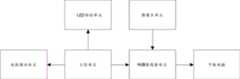
图1是本发明的原理框图。Fig. 1 is a principle block diagram of the present invention.
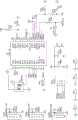
图2是本发明的电机驱动单元的电路原理图。FIG. 2 is a schematic circuit diagram of the motor drive unit of the present invention.
图3是本发明的LED驱动单元的电路原理图。FIG. 3 is a schematic circuit diagram of the LED driving unit of the present invention.
图4是本发明的主控单元的电路原理图。FIG. 4 is a schematic circuit diagram of the main control unit of the present invention.
图5是本发明摄像头单元的电路原理图。FIG. 5 is a circuit schematic diagram of the camera unit of the present invention.
图6是本发明HUB集线器单元的电路原理图。FIG. 6 is a schematic circuit diagram of the HUB hub unit of the present invention.
具体实施方式Detailed ways
下面结合附图对本发明作进一步详细的说明。The present invention will be described in further detail below in conjunction with the accompanying drawings.
如图1所示,一种采集头部皮肤图像装置的原理框图,此装置由电机驱动单元、LED驱动单元、主控单元、摄像头单元、HUB集线器单元、平板电脑构成。本实施例采用平板电脑作为上位机。电机驱动单元用于驱动步进电机,由步进电机带动摄像头前进后退,从而实现自动对焦的功能。LED驱动单元用于控制LED光源熄灭或者点亮状态,为摄像头提供光源。主控单元连接LED驱动单元和电机驱动单元,用于控制电机运动和LED灯的状态,并且主控单元通过HUB集线器单元连接到平板电脑,与平板电脑进行数据交互。摄像头单元用于采集图像,通过HUB集线器单元连接到平板电脑,把图像传输到平板电脑。HUB集线器单元把主控单元和摄像头单元通过USB总线,连接到平板电脑。平板电脑通过HUB集线器采集摄像头单元的图像,并且通过HUB集线器单元连接主控单元,从而控制电机和LED光源。As shown in Figure 1, a schematic block diagram of a device for collecting head skin images, the device consists of a motor drive unit, an LED drive unit, a main control unit, a camera unit, a HUB hub unit, and a tablet computer. In this embodiment, a tablet computer is used as the upper computer. The motor drive unit is used to drive the stepper motor, and the stepper motor drives the camera forward and backward, so as to realize the function of automatic focusing. The LED drive unit is used to control the LED light source to be turned off or on, and to provide a light source for the camera. The main control unit is connected to the LED drive unit and the motor drive unit for controlling the motor movement and the state of the LED lights, and the main control unit is connected to the tablet computer through the HUB hub unit for data interaction with the tablet computer. The camera unit is used to capture images, and is connected to the tablet computer through the HUB hub unit to transmit the image to the tablet computer. The HUB hub unit connects the main control unit and the camera unit to the tablet computer through the USB bus. The tablet computer collects the image of the camera unit through the HUB hub, and connects the main control unit through the HUB hub unit, so as to control the motor and the LED light source.
如图2所示,为电机驱动单元的电路图,由两个电机驱动芯片L293DD,即U1、U2控制步进电机,U1用于控制步进电机,实现摄像头的变焦功能;U2用于控制步进电机,实现摄像头的聚焦功能。通过端子P3连接到步进电机。通过端子P2连接到主控单元的I/O引脚。U4用于降压,把5V降低为3.3V,电容C1、C3是U4的电源输入侧的滤波电容,电容C2、C4是U4电源输出侧的滤波电容。端子P1用于选择U1、U2的电源为5V或者3.3V。As shown in Figure 2, it is the circuit diagram of the motor drive unit. Two motor drive chips L293DD are used to control the stepping motor, namely U1 and U2. U1 is used to control the stepping motor to realize the zoom function of the camera; U2 is used to control the stepping motor. The motor realizes the focusing function of the camera. Connect to the stepper motor via terminal P3. Connect to the I/O pins of the main control unit via terminal P2. U4 is used to step down and reduce 5V to 3.3V. Capacitors C1 and C3 are the filter capacitors on the input side of the power supply of U4, and capacitors C2 and C4 are the filter capacitors on the output side of the power supply of U4. Terminal P1 is used to select the power supply of U1 and U2 as 5V or 3.3V.
如图3所示,为LED驱动单元的电路,电路由三个MP3302DJ-LE-Z,即U1、U2、U3构成三路LED驱动电路,三路LED驱动原理一致,现在选取U1分析其驱动原理。U1的EN引脚通过电阻R1下拉到GND,默认使U1处于关闭状态,LED熄灭,EN连接到电阻R7,电阻R7的另一端连接到控制信号R-DIM,R-DIM连接到主控单元的IO引脚,主控单元输出高电平给R-DIM,LED点亮;主控单元输出低电平给R-DIM,LED熄灭。U1的FB引脚连接到电阻R2,电阻R2的另一端连接到GND,用于调节LED的亮度。As shown in Figure 3, it is the circuit of the LED drive unit. The circuit consists of three MP3302DJ-LE-Z, namely U1, U2, and U3 to form a three-way LED drive circuit. The three-way LED driving principle is the same. Now select U1 to analyze its driving principle . The EN pin of U1 is pulled down to GND through the resistor R1. By default, U1 is turned off, the LED is off, EN is connected to the resistor R7, the other end of the resistor R7 is connected to the control signal R-DIM, and R-DIM is connected to the main control unit. IO pin, the main control unit outputs a high level to R-DIM, and the LED turns on; the main control unit outputs a low level to R-DIM, and the LED turns off. The FB pin of U1 is connected to resistor R2 and the other end of resistor R2 is connected to GND for adjusting the brightness of the LED.
U1的FB引脚同时连接到CN1的RGB-端。U1的IN引脚连接到电源+5V,电容C1作为U1的IN引脚的滤波电容。电感L1的一端连接到电源+5V,另一端连接到U1的SW引脚;肖特基二极管D1的一端连接到U1的SW引脚,另一端连接到CN1的RGB+端。端子CN1连接到LED的正负极。U2的EN引脚通过电阻R3下拉到GND,默认使U2处于关闭状态,LED熄灭;EN连接到电阻R8,电阻R8的另一端连接到控制信号G-DIM,G-DIM连接到主控单元的IO引脚,主控单元输出高电平给G-DIM,LED点亮,主控单元输出低电平给G-DIM,LED熄灭;U2的FB引脚连接到电阻R4,电阻R4的另一端连接到GND,用于调节LED的亮度,U2的FB引脚同时连接到CN1的FP-端,U2的IN引脚连接到电源+5V;电感L2的一端连接到电源+5V,另一端连接到U2的SW引脚;肖特基二极管D2的一端连接到U2的SW引脚,另一端连接到CN1的FP+端,端子CN1连接到LED的正负极;U3的EN引脚通过电阻R5下拉到GND,默认使U3处于关闭状态,LED熄灭;EN连接到电阻R9,电阻R9的另一端连接到控制信号B-DIM,B-DIM连接到主控单元的IO引脚,主控单元输出高电平给B-DIM,LED点亮,主控单元输出低电平给B-DIM,LED熄灭;U3的FB引脚连接到电阻R6,电阻R6的另一端连接到GND,用于调节LED的亮度,U3的FB引脚同时连接到CN1的UV-端,U3的IN引脚连接到电源+5V;电感L3的一端连接到电源+5V,另一端连接到U3的SW引脚;肖特基二极管D3的一端连接到U3的SW引脚,另一端连接到CN1的UV+端,端子CN1连接到LED的正负极。所述LED驱动芯片U1、U2、U3的芯片型号为MP3302DJ-LE-Z。The FB pin of U1 is also connected to the RGB- terminal of CN1. The IN pin of U1 is connected to the power supply +5V, and the capacitor C1 acts as a filter capacitor for the IN pin of U1. One end of the inductor L1 is connected to the power supply +5V, and the other end is connected to the SW pin of U1; one end of the Schottky diode D1 is connected to the SW pin of U1, and the other end is connected to the RGB+ end of CN1. Terminal CN1 is connected to the positive and negative poles of the LED. The EN pin of U2 is pulled down to GND through the resistor R3. By default, U2 is turned off and the LED is off; EN is connected to the resistor R8, the other end of the resistor R8 is connected to the control signal G-DIM, and G-DIM is connected to the main control unit. IO pin, the main control unit outputs a high level to G-DIM, the LED is on, the main control unit outputs a low level to G-DIM, and the LED is off; the FB pin of U2 is connected to the resistor R4, the other end of the resistor R4 Connect to GND to adjust the brightness of the LED, the FB pin of U2 is connected to the FP- end of CN1 at the same time, the IN pin of U2 is connected to the power supply +5V; one end of the inductor L2 is connected to the power supply +5V, and the other end is connected to the power supply +5V. The SW pin of U2; one end of the Schottky diode D2 is connected to the SW pin of U2, the other end is connected to the FP+ end of CN1, and the terminal CN1 is connected to the positive and negative poles of the LED; the EN pin of U3 is pulled down by the resistor R5 to GND, U3 is turned off by default, LED is off; EN is connected to resistor R9, the other end of resistor R9 is connected to control signal B-DIM, B-DIM is connected to the IO pin of the main control unit, the main control unit outputs high power Flat to B-DIM, the LED is on, the main control unit outputs a low level to B-DIM, and the LED is off; the FB pin of U3 is connected to the resistor R6, and the other end of the resistor R6 is connected to GND to adjust the brightness of the LED , The FB pin of U3 is connected to the UV- terminal of CN1 at the same time, the IN pin of U3 is connected to the power supply +5V; one end of the inductor L3 is connected to the power supply +5V, and the other end is connected to the SW pin of U3; Schottky diode One end of D3 is connected to the SW pin of U3, the other end is connected to the UV+ end of CN1, and the terminal CN1 is connected to the positive and negative poles of the LED. The chip model of the LED driver chips U1, U2 and U3 is MP3302DJ-LE-Z.
如图4所示,为主控单元电路,U8用于控制电机单元和LED灯驱动单元。电阻R16和电容C8构成U8的上电复位电路。电容C10是U8的电源滤波电容,电容是U8的VCAP引脚的旁路电容。U8通过P6端口连接到电机驱动单元的控制引脚。通过R-DIM、G-DIM、B-DIM连接到LED灯驱动单元的控制引脚。U8的TXD、RXD引脚连接到U7的RXD、TXD引脚。U7通过UD+和UD-连接到HUB集线器电路。As shown in Figure 4, as the main control unit circuit, U8 is used to control the motor unit and the LED lamp drive unit. Resistor R16 and capacitor C8 constitute the power-on reset circuit of U8. Capacitor C10 is the power filter capacitor of U8, and the capacitor is the bypass capacitor of the VCAP pin of U8. U8 is connected to the control pins of the motor drive unit through the P6 port. Connect to the control pins of the LED lamp driver unit through R-DIM, G-DIM, B-DIM. The TXD and RXD pins of U8 are connected to the RXD and TXD pins of U7. U7 is connected to the HUB hub circuit via UD+ and UD-.
如图5所示,为摄像头单元的电路,电路由DSP主控芯片U2、感光芯片U1和EEPROM芯片U3构成。按键S1是拍照按键,按键S1一侧连接到GND,另外一侧通过电阻R2连接到V3.3电源,按下按键S1拍照。电容C12、C17、C18、C20、C22、C14为V3.3的滤波电容;电容C13、C15为V1.8的滤波电容;电容C7、C8、C9为AVDD33的滤波电容;电容C5、C6为AVDD5的滤波电容。电阻R3、R4、R5为U3的上拉电阻。摄像头单元电路通过CON-USB端口连接到HUB集线器单元电路。As shown in Figure 5, it is the circuit of the camera unit, and the circuit is composed of a DSP main control chip U2, a photosensitive chip U1 and an EEPROM chip U3. The button S1 is a camera button, one side of the button S1 is connected to GND, and the other side is connected to the V3.3 power supply through the resistor R2, and the button S1 is pressed to take a picture. Capacitors C12, C17, C18, C20, C22, and C14 are filter capacitors of V3.3; capacitors C13 and C15 are filter capacitors of V1.8; capacitors C7, C8, and C9 are filter capacitors of AVDD33; capacitors C5 and C6 are AVDD5 filter capacitor. Resistors R3, R4, and R5 are pull-up resistors for U3. The camera unit circuit is connected to the HUB hub unit circuit through the CON-USB port.
如图6所示,为HUB集线器电路,电容C12、C13、C14为U5的电源滤波电容;晶体振荡器X1为U5提供震荡源;U5的OVCJ引脚通过电阻R10上拉的+5V电源,并且通过电容C4滤波。U5的XRSTJ引脚通过电阻R14连接到VDD33_O,电容C5为VDD33_O的滤波电容。U5的BUSM引脚通过电阻R15连接到+5V电源。HUB集线器单元通过CON3连接到主控单元电路的U7;通过CON2连接到摄像头单元;通过CON1连接到平板电脑。As shown in Figure 6, it is a HUB hub circuit. Capacitors C12, C13, and C14 are the power supply filter capacitors of U5; the crystal oscillator X1 provides the oscillation source for U5; the OVCJ pin of U5 is pulled up by the resistor R10 +5V power supply, and Filtered by capacitor C4. The XRSTJ pin of U5 is connected to VDD33_O through resistor R14, and capacitor C5 is the filter capacitor of VDD33_O. The BUSM pin of U5 is connected to the +5V supply through resistor R15. The HUB hub unit is connected to U7 of the main control unit circuit through CON3; connected to the camera unit through CON2; connected to the tablet computer through CON1.
以上的实施例只是在于说明而不是限制本发明,故凡依本发明专利申请范围所述的方法所做的等效变化或修饰,均包括于本发明专利申请范围内。The above embodiments are only intended to illustrate rather than limit the present invention, so all equivalent changes or modifications made according to the methods described in the scope of the patent application of the present invention are included in the scope of the patent application of the present invention.
Claims (10)
Priority Applications (1)
| Application Number | Priority Date | Filing Date | Title |
|---|---|---|---|
| CN201911075940.6ACN110664379A (en) | 2019-11-06 | 2019-11-06 | A device for collecting images of human head skin |
Applications Claiming Priority (1)
| Application Number | Priority Date | Filing Date | Title |
|---|---|---|---|
| CN201911075940.6ACN110664379A (en) | 2019-11-06 | 2019-11-06 | A device for collecting images of human head skin |
Publications (1)
| Publication Number | Publication Date |
|---|---|
| CN110664379Atrue CN110664379A (en) | 2020-01-10 |
Family
ID=69086299
Family Applications (1)
| Application Number | Title | Priority Date | Filing Date |
|---|---|---|---|
| CN201911075940.6APendingCN110664379A (en) | 2019-11-06 | 2019-11-06 | A device for collecting images of human head skin |
Country Status (1)
| Country | Link |
|---|---|
| CN (1) | CN110664379A (en) |
Citations (6)
| Publication number | Priority date | Publication date | Assignee | Title |
|---|---|---|---|---|
| CN104883970A (en)* | 2012-12-21 | 2015-09-02 | Amc有限公司 | Skin condition measuring device for smartphone |
| CN206252493U (en)* | 2016-08-30 | 2017-06-16 | 深圳斯坦普光生物科技有限公司 | A kind of skin analysis device based on microspur high-definition camera |
| CN208337720U (en)* | 2018-06-11 | 2019-01-04 | 昆山星际舟智能科技有限公司 | Vehicle-mounted camera Automatic zoom lens focusing device |
| CN208819225U (en)* | 2018-11-02 | 2019-05-03 | 广州市皓品信息科技有限公司 | A kind of two-way camera lens skin image capture means |
| CN209330236U (en)* | 2019-02-27 | 2019-08-30 | 广州市皓品信息科技有限公司 | The skin image sampling apparatus of adjustable light sources brightness |
| CN211883750U (en)* | 2019-11-06 | 2020-11-10 | 广州市皓品信息科技有限公司 | Device for collecting human head skin image |
- 2019
- 2019-11-06CNCN201911075940.6Apatent/CN110664379A/enactivePending
Patent Citations (6)
| Publication number | Priority date | Publication date | Assignee | Title |
|---|---|---|---|---|
| CN104883970A (en)* | 2012-12-21 | 2015-09-02 | Amc有限公司 | Skin condition measuring device for smartphone |
| CN206252493U (en)* | 2016-08-30 | 2017-06-16 | 深圳斯坦普光生物科技有限公司 | A kind of skin analysis device based on microspur high-definition camera |
| CN208337720U (en)* | 2018-06-11 | 2019-01-04 | 昆山星际舟智能科技有限公司 | Vehicle-mounted camera Automatic zoom lens focusing device |
| CN208819225U (en)* | 2018-11-02 | 2019-05-03 | 广州市皓品信息科技有限公司 | A kind of two-way camera lens skin image capture means |
| CN209330236U (en)* | 2019-02-27 | 2019-08-30 | 广州市皓品信息科技有限公司 | The skin image sampling apparatus of adjustable light sources brightness |
| CN211883750U (en)* | 2019-11-06 | 2020-11-10 | 广州市皓品信息科技有限公司 | Device for collecting human head skin image |
Similar Documents
| Publication | Publication Date | Title |
|---|---|---|
| CN201788518U (en) | Identification device with facial image and iris image acquisition functions | |
| CN111435968B (en) | Camera and control method thereof | |
| CN102914667A (en) | Large-scale particle image velocimeter based on near-infrared smart camera | |
| CN211883750U (en) | Device for collecting human head skin image | |
| CN111714081A (en) | Optical nondestructive testing instrument and detection method for special children based on multi-wavelength LED | |
| CN203552276U (en) | Facial recognition device applicable to wide-dynamic-range ambient light | |
| CN110664379A (en) | A device for collecting images of human head skin | |
| CN115240251A (en) | Method for realizing live broadcast light supplement lamp for face tracking illumination and light supplement lamp thereof | |
| CN109460686B (en) | Method and system for blanking aiming light of aiming device | |
| CN208312129U (en) | Light compensating apparatus applied to facial diagnosis Image Acquisition | |
| CN110598661A (en) | Palmprint and palmar vein acquisition system | |
| CN202949497U (en) | Focusing speed automatic control device for telephoto lenses | |
| CN206462971U (en) | A kind of Portable fundus camera circuit system | |
| CN117576756B (en) | Bathroom mirror with face detail capturing and amplifying functions | |
| CN215642742U (en) | Multimodal Biometric Module and Multimodal Biometric Device | |
| CN221039833U (en) | Automatic lens pressing control system | |
| CN201255787Y (en) | Electronic spectacle | |
| CN207022096U (en) | A kind of image collecting device | |
| CN108332718B (en) | Structured light information acquisition system | |
| CN112709943A (en) | Artificial intelligence operation shadowless lamp | |
| CN208834326U (en) | A kind of iris image extraction element based on liquid lens and VCM | |
| CN211427357U (en) | Device for automatically detecting human body characteristics | |
| CN109101959A (en) | A kind of iris image extraction element based on liquid lens and VCM | |
| CN119896438A (en) | Endoscope light source system and endoscope | |
| CN106657756A (en) | Camera hoop based on brain wave control |
Legal Events
| Date | Code | Title | Description |
|---|---|---|---|
| PB01 | Publication | ||
| PB01 | Publication | ||
| SE01 | Entry into force of request for substantive examination | ||
| SE01 | Entry into force of request for substantive examination | ||
| RJ01 | Rejection of invention patent application after publication | Application publication date:20200110 | |
| RJ01 | Rejection of invention patent application after publication |