CN110660792A - The generation method and layout layout method of filling pattern of FDSOI standard cell - Google Patents
The generation method and layout layout method of filling pattern of FDSOI standard cellDownload PDFInfo
- Publication number
- CN110660792A CN110660792ACN201910938131.7ACN201910938131ACN110660792ACN 110660792 ACN110660792 ACN 110660792ACN 201910938131 ACN201910938131 ACN 201910938131ACN 110660792 ACN110660792 ACN 110660792A
- Authority
- CN
- China
- Prior art keywords
- fdsoi
- parameters
- standard
- filling
- cell
- Prior art date
- Legal status (The legal status is an assumption and is not a legal conclusion. Google has not performed a legal analysis and makes no representation as to the accuracy of the status listed.)
- Granted
Links
Images


Classifications
- H—ELECTRICITY
- H10—SEMICONDUCTOR DEVICES; ELECTRIC SOLID-STATE DEVICES NOT OTHERWISE PROVIDED FOR
- H10D—INORGANIC ELECTRIC SEMICONDUCTOR DEVICES
- H10D89/00—Aspects of integrated devices not covered by groups H10D84/00 - H10D88/00
- H10D89/10—Integrated device layouts
Landscapes
- Design And Manufacture Of Integrated Circuits (AREA)
Abstract
Description
Translated fromChinese技术领域technical field
本申请涉及半导体制造技术领域,具体涉及一种FDSOI标准单元的填充图形的生成方法以及版图布局方法。The present application relates to the technical field of semiconductor manufacturing, and in particular, to a method for generating filling patterns of FDSOI standard cells and a method for layout layout.
背景技术Background technique
标准单元库,其包括版图库、符号库、电路逻辑库等,其包含了组合逻辑、时序逻辑、功能单元和特殊类型单元,是集成电路芯片后端设计过程中的基础部分。可运用标准单元库中预先设计好的标准单元进行自动逻辑综合和版图布局布线,可以极大地提高设计效率。The standard cell library, which includes layout library, symbol library, circuit logic library, etc., includes combinational logic, sequential logic, functional units and special types of units, and is the basic part of the back-end design process of integrated circuit chips. The pre-designed standard cells in the standard cell library can be used for automatic logic synthesis and layout layout, which can greatly improve the design efficiency.
全耗尽绝缘硅(Fully Depleted Silicon On Insulator,FDSOI)结构是将晶体管设置于绝缘硅(SOI)上的半导体结构,FDSOI结构由于在晶体管之间加入绝缘物质,使两者之间的寄生电容大幅度降低,从而减小了器件的寄生电容,降低了漏电流。示例性的,如图1所示,定义N型(Negative)衬底的P型金属氧化物半导体场效应晶体管(Positive channelMetal Oxide Semiconductor,PMOS)和P型衬底的NMOS构成的FDSOI结构为RVT器件100;如图2所示,定义P型衬底的PMOS和N型衬底的NMOS构成的FDSOI结构为LVT器件200;如图3所示,定义N型衬底的PMOS和NMOS构成的FDSOI结构为SNW器件300;如图4所示,定义P型衬底的PMOS和NMOS构成的FDSOI结构为SPW器件400。图1至图4中,101为金属层(Tap),102为栅极(Gate),103为浅槽隔离(Shallow Trench Isolation,STI)结构,104为绝缘层(Box)。Fully Depleted Silicon On Insulator (FDSOI) structure is a semiconductor structure in which transistors are arranged on silicon-on-insulator (SOI). The FDSOI structure has a large parasitic capacitance due to the addition of insulating substances between transistors. The amplitude is reduced, thereby reducing the parasitic capacitance of the device and reducing the leakage current. Exemplarily, as shown in FIG. 1 , the FDSOI structure composed of a P-type metal oxide semiconductor field effect transistor (Positive channel Metal Oxide Semiconductor, PMOS) of a N-type (Negative) substrate and an NMOS of a P-type substrate is defined as an RVT device. 100; As shown in FIG. 2, the FDSOI structure composed of the PMOS of the P-type substrate and the NMOS of the N-type substrate is defined as the
如图5所示,以RVT器件和LVT器件为例,由于两种器件的衬底掺杂类型相反,因此,在二者邻接时,会在中线位置产生奇点501,造成拼接问题。As shown in FIG. 5 , taking an RVT device and an LVT device as examples, since the substrate doping types of the two devices are opposite, when the two devices are adjacent to each other, a singularity 501 will be generated at the centerline position, causing a splicing problem.
针对上述问题,相关技术中通常将不同类型的器件(例如RVT器件和LVT器件)进行分区布局,但是会带来极大的面积浪费。In view of the above problems, different types of devices (for example, RVT devices and LVT devices) are usually partitioned and laid out in the related art, but this will bring about a great waste of area.
发明内容SUMMARY OF THE INVENTION
本申请提供了一种FDSOI标准单元的填充图形的生成方法以及版图布局方法,可以解决相关技术中提供的FDSOI版图结构由于将不同类型的器件进行分区布局所导致面积浪费的问题。The present application provides a method for generating filling patterns of FDSOI standard cells and a layout layout method, which can solve the problem of area waste caused by partitioning layout of different types of devices in the FDSOI layout structure provided in the related art.
一方面,本申请实施例提供了一种FDSOI标准单元的填充图形的生成方法,其特征在于,所述方法应用于半导体制造,所述方法包括:On the one hand, an embodiment of the present application provides a method for generating a filling pattern of an FDSOI standard cell, wherein the method is applied to semiconductor manufacturing, and the method includes:
获取标准单元库中FDSOI标准单元的参数;Get the parameters of the FDSOI standard cell in the standard cell library;
根据所述FDSOI标准单元的参数确定填充单元的参数;Determine the parameters of the filling unit according to the parameters of the FDSOI standard unit;
根据所述填充单元的参数生成FDSOI标准单元的填充图形。The filling pattern of the FDSOI standard cell is generated according to the parameters of the filling cell.
可选的,所述FDSOI标准单元的参数包括所述FDSOI标准单元的高度,所述填充单元的参数包括所述填充单元的高度;Optionally, the parameter of the FDSOI standard unit includes the height of the FDSOI standard unit, and the parameter of the filling unit includes the height of the filling unit;
所述根据所述FDSOI标准单元的参数确定填充单元的参数,包括:The parameters of the filling unit are determined according to the parameters of the FDSOI standard unit, including:
将所述填充单元的高度确定为所述FDSOI标准单元的高度。The height of the filling unit is determined as the height of the FDSOI standard unit.
可选的,所述FDSOI标准单元的参数包括所述FDSOI标准单元的N型阱边线,所述填充单元的参数包括所述填充单元的N型阱区域;Optionally, the parameter of the FDSOI standard cell includes an N-type well edge of the FDSOI standard cell, and the parameter of the filling unit includes an N-type well region of the filling unit;
所述根据所述FDSOI标准单元的参数确定填充单元的参数,包括:The parameters of the filling unit are determined according to the parameters of the FDSOI standard unit, including:
根据所述FDSOI标准单元的N型阱边线确定所述填充单元的N型阱区域。The N-type well region of the filled cell is determined according to the N-type well edge of the FDSOI standard cell.
可选的,所述FDSOI标准单元的参数包括阱识别层边线,所述填充单元的参数包括所述填充单元的N型阱取反区域和P型阱取反区域;Optionally, the parameters of the FDSOI standard cell include a well identification layer edge, and the parameters of the filling unit include an N-type well inversion region and a P-type well inversion region of the filling cell;
所述根据所述FDSOI标准单元的参数确定填充单元的参数,包括:The parameters of the filling unit are determined according to the parameters of the FDSOI standard unit, including:
根据所述阱识别层边线确定所述填充单元的N型阱取反区域和P型阱取反区域。The N-type well inversion region and the P-type well inversion region of the filled cell are determined according to the edge of the well identification layer.
可选的,所述FDSOI标准单元的参数包括所述FDSOI标准单元的水平布线间距,所述填充单元的参数包括所述填充单元的横向最小布线轨道间隔尺寸;Optionally, the parameter of the FDSOI standard cell includes the horizontal wiring spacing of the FDSOI standard cell, and the parameter of the filling unit includes the horizontal minimum wiring track spacing size of the filling unit;
所述根据所述FDSOI标准单元的参数确定填充单元的参数,包括:The parameters of the filling unit are determined according to the parameters of the FDSOI standard unit, including:
将所述填充单元的横向最小布线轨道间隔尺寸确定为所述FDSOI标准单元的水平布线间距。The lateral minimum wiring track spacing dimension of the filled cell is determined as the horizontal wiring pitch of the FDSOI standard cell.
可选的,所述FDSOI标准单元的参数包括所述FDSOI标准单元的垂直布线间距,所述填充单元的参数包括所述填充单元的竖向最小布线轨道间隔尺寸;Optionally, the parameter of the FDSOI standard cell includes a vertical wiring spacing of the FDSOI standard cell, and the parameter of the filling unit includes a vertical minimum wiring track spacing dimension of the filling unit;
所述根据所述FDSOI标准单元的参数确定填充单元的参数,包括:The parameters of the filling unit are determined according to the parameters of the FDSOI standard unit, including:
将所述填充单元的竖向最小布线轨道间隔尺寸确定为所述FDSOI标准单元的垂直布线间距。The vertical minimum wiring track spacing dimension of the filled cell is determined as the vertical wiring pitch of the FDSOI standard cell.
另一方面,本申请提供了一种FDSOI标准单元库的版图布局方法,包括:On the other hand, the present application provides a layout layout method of an FDSOI standard cell library, including:
确定需要插入填充单元的插入位置;Determine the insertion position where the filling unit needs to be inserted;
根据所述插入位置两侧的FDSOI标准单元确定需要插入的填充单元,所述填充单元是根据上述任一方法生成得到的;Determine the filling unit to be inserted according to the FDSOI standard cells on both sides of the insertion position, and the filling unit is generated according to any of the above methods;
在所述插入位置插入所述需要插入的填充单元,生成FDSOI标准单元库的版图以实现所述FDSOI标准单元的版图拼接。Insert the filling cell to be inserted at the insertion position, and generate the layout of the FDSOI standard cell library to realize the layout splicing of the FDSOI standard cell.
本申请技术方案,至少包括如下优点:The technical solution of the present application includes at least the following advantages:
通过根据FDSOI标准单元的参数确定填充单元的参数,根据填充单元的参数生成FDSOI标准单元的填充单元,由于填充单元的参数是基于FDSOI标准单元的参数确定的,因此能够解决不同类型的FDSOI器件之间的拼接问题,实现了不同类型的FDSOI器件在同一张晶圆上制备,降低了生产成本。By determining the parameters of the filling unit according to the parameters of the FDSOI standard unit, and generating the filling unit of the FDSOI standard unit according to the parameters of the filling unit, since the parameters of the filling unit are determined based on the parameters of the FDSOI standard unit, it can solve the problem of different types of FDSOI devices. The problem of splicing between different types of FDSOI devices is realized on the same wafer, which reduces the production cost.
附图说明Description of drawings
为了更清楚地说明本申请具体实施方式或现有技术中的技术方案,下面将对具体实施方式或现有技术描述中所需要使用的附图作简单地介绍,显而易见地,下面描述中的附图是本申请的一些实施方式,对于本领域普通技术人员来讲,在不付出创造性劳动的前提下,还可以根据这些附图获得其他的附图。In order to more clearly illustrate the specific embodiments of the present application or the technical solutions in the prior art, the accompanying drawings that need to be used in the description of the specific embodiments or the prior art will be briefly introduced below. The drawings are some embodiments of the present application. For those of ordinary skill in the art, other drawings can also be obtained from these drawings without any creative effort.
图1是RVT器件的结构示意图;Fig. 1 is the structural schematic diagram of RVT device;
图2是LVT器件的结构示意图;Fig. 2 is the structure schematic diagram of LVT device;
图3是SNW器件的结构示意图;Fig. 3 is the structural schematic diagram of SNW device;
图4是SPW器件的结构示意图;Fig. 4 is the structure schematic diagram of SPW device;
图5是RVT器件和LVT器件拼接的版图示意图;Fig. 5 is the layout schematic diagram of RVT device and LVT device splicing;
图6是本申请一个示例性实施例提供的FDSOI标准单元的填充图形的生成方法的流程图;6 is a flowchart of a method for generating a fill pattern of an FDSOI standard cell provided by an exemplary embodiment of the present application;
图7是本申请一个示例性实施例提供的FDSOI标准单元库的版图布局方法的流程图;7 is a flowchart of a layout layout method of an FDSOI standard cell library provided by an exemplary embodiment of the present application;
图8示出了基于本申请实施例提供的FDSOI标准单元的填充图形的生成方法生成的插入LVT器件和RVT器件的填充单元的版图示意图;8 shows a schematic layout diagram of a filled cell inserted into an LVT device and an RVT device generated based on the method for generating a filling pattern of an FDSOI standard cell provided by an embodiment of the present application;
图9示出了基于本申请实施例提供的FDSOI标准单元的填充图形的生成方法生成的插入LVT器件和RVT器件的填充单元的版图示意图;9 shows a schematic layout diagram of a filled cell inserted into an LVT device and an RVT device generated based on the method for generating a filling pattern of an FDSOI standard cell provided by an embodiment of the present application;
图10示出了基于本申请实施例提供的标准单元的填充图形的生成方法生成的插入SNW器件和RVT器件的填充单元的版图示意图;10 shows a schematic layout diagram of a filled cell inserted into an SNW device and an RVT device generated based on the method for generating a filling pattern of a standard cell provided by an embodiment of the present application;
图11示出了基于本申请实施例提供的FDSOI标准单元的填充图形的生成方法生成的插入SNW器件和LVT器件的填充单元的版图示意图;11 shows a schematic layout diagram of a filled cell inserted into an SNW device and an LVT device generated based on the method for generating a filling pattern of an FDSOI standard cell provided by an embodiment of the present application;
图12示出了基于本申请实施例提供的FDSOI标准单元的填充图形的生成方法生成的插入SPW器件和RVT器件的填充单元的版图示意图;12 shows a schematic layout diagram of the filled cells inserted into the SPW device and the RVT device generated based on the method for generating the filling pattern of the FDSOI standard cell provided by the embodiment of the present application;
图13示出了基于本申请实施例提供的FDSOI标准单元的填充图形的生成方法生成的插入SPW器件和LVT器件的填充单元的版图示意图。FIG. 13 shows a schematic layout diagram of a filled cell inserted into an SPW device and an LVT device generated based on the method for generating a filling pattern of an FDSOI standard cell provided by an embodiment of the present application.
具体实施方式Detailed ways
下面将结合附图,对本申请中的技术方案进行清楚、完整的描述,显然,所描述的实施例是本申请的一部分实施例,而不是全部的实施例。基于本申请中的实施例,本领域普通技术人员在不做出创造性劳动的前提下所获得的所有其它实施例,都属于本申请保护的范围。The technical solutions in the present application will be clearly and completely described below with reference to the accompanying drawings. Obviously, the described embodiments are a part of the embodiments of the present application, but not all of the embodiments. Based on the embodiments in the present application, all other embodiments obtained by those of ordinary skill in the art without creative work fall within the protection scope of the present application.
在本申请的描述中,需要说明的是,术语“中心”、“上”、“下”、“左”、“右”、“竖直”、“水平”、“内”、“外”等指示的方位或位置关系为基于附图所示的方位或位置关系,仅是为了便于描述本申请和简化描述,而不是指示或暗示所指的装置或元件必须具有特定的方位、以特定的方位构造和操作,因此不能理解为对本申请的限制。此外,术语“第一”、“第二”、“第三”仅用于描述目的,而不能理解为指示或暗示相对重要性。In the description of this application, it should be noted that the terms "center", "upper", "lower", "left", "right", "vertical", "horizontal", "inner", "outer", etc. The indicated orientation or positional relationship is based on the orientation or positional relationship shown in the accompanying drawings, which is only for the convenience of describing the present application and simplifying the description, rather than indicating or implying that the indicated device or element must have a specific orientation or a specific orientation. construction and operation, and therefore should not be construed as limitations on this application. Furthermore, the terms "first", "second", and "third" are used for descriptive purposes only and should not be construed to indicate or imply relative importance.
在本申请的描述中,需要说明的是,除非另有明确的规定和限定,术语“安装”、“相连”、“连接”应做广义理解,例如,可以是固定连接,也可以是可拆卸连接,或一体地连接;可以是机械连接,也可以是电气连接;可以是直接相连,也可以通过中间媒介间接相连,还可以是两个元件内部的连通,可以是无线连接,也可以是有线连接。对于本领域的普通技术人员而言,可以具体情况理解上述术语在本申请中的具体含义。In the description of this application, it should be noted that, unless otherwise expressly specified and limited, the terms "installed", "connected" and "connected" should be understood in a broad sense, for example, it may be a fixed connection or a detachable connection connection, or integral connection; it can be a mechanical connection or an electrical connection; it can be a direct connection or an indirect connection through an intermediate medium, or it can be the internal connection of two components, which can be a wireless connection or a wired connection connect. For those of ordinary skill in the art, the specific meanings of the above terms in this application can be understood in specific situations.
此外,下面所描述的本申请不同实施方式中所涉及的技术特征只要彼此之间未构成冲突就可以相互结合。In addition, the technical features involved in the different embodiments of the present application described below can be combined with each other as long as there is no conflict with each other.
本申请中,定义FDSOI标准单元的高度所在方向为Z轴,定义版图的垂直方向为Y轴,定义版图的水平方向为X轴。In this application, the direction of the height of the FDSOI standard cell is defined as the Z axis, the vertical direction of the layout is defined as the Y axis, and the horizontal direction of the layout is defined as the X axis.
实施例1:Example 1:
图6是本申请一个示例性实施例提供的FDSOI标准单元的填充图形的生成方法,该方法应用于半导体制造,该方法包括:6 is a method for generating a filling pattern of an FDSOI standard cell provided by an exemplary embodiment of the present application. The method is applied to semiconductor manufacturing, and the method includes:
步骤601,获取标准单元库中FDSOI标准单元的参数。Step 601: Acquire the parameters of the FDSOI standard cell in the standard cell library.
其中,FDSOI标准单元的参数包括FDSOI标准单元的高度、N型阱(Well)边线、阱识别层(Well-Reverse)边线、水平布线间距以及垂直布线间距中的至少一种;FDSOI标准单元包括RVT器件、LVT器件、SNW器件以及SPW器件中的至少两种。The parameters of the FDSOI standard cell include at least one of the height of the FDSOI standard cell, the N-type well (Well) edge, the well identification layer (Well-Reverse) edge, the horizontal wiring spacing and the vertical wiring spacing; the FDSOI standard cell includes RVT At least two of the device, the LVT device, the SNW device, and the SPW device.
步骤602,根据FDSOI标准单元的参数确定填充单元的参数。Step 602: Determine the parameters of the filling unit according to the parameters of the FDSOI standard unit.
其中,填充单元是设置于FDSOI标准单元之间的结构;填充单元的参数包括填充单元的高度、N型阱区域、N型阱取反区域、P型阱取反区域、横向最小布线轨道间隔尺寸以及竖向最小布线轨道间隔尺寸中的至少一种。Among them, the filling unit is a structure arranged between the FDSOI standard cells; the parameters of the filling unit include the height of the filling unit, the N-type well region, the N-type well inversion region, the P-type well inversion region, and the minimum horizontal wiring track spacing size and at least one of the vertical minimum wiring track spacing dimensions.
步骤603,根据填充单元的参数生成FDSOI标准单元的填充图形。Step 603: Generate a filling pattern of the FDSOI standard cell according to the parameters of the filling cell.
综上所述,本实施例中,通过根据FDSOI标准单元的参数确定填充单元的参数,根据填充单元的参数自动生成FDSOI标准单元的填充单元,由于填充单元的参数是基于FDSOI标准单元的参数确定的,因此能够解决不同类型的FDSOI器件之间的拼接问题,实现了不同类型的FDSOI器件在同一张晶圆上制备,降低了生产成本。To sum up, in this embodiment, the parameters of the filling unit are determined according to the parameters of the FDSOI standard unit, and the filling unit of the FDSOI standard unit is automatically generated according to the parameters of the filling unit, because the parameters of the filling unit are determined based on the parameters of the FDSOI standard unit. Therefore, it can solve the problem of splicing between different types of FDSOI devices, realize the preparation of different types of FDSOI devices on the same wafer, and reduce the production cost.
实施例2:Example 2:
参考实施例1,实施例2和实施例1的区别在于:对于步骤602中的“根据FDSOI标准单元的参数确定填充单元的参数”,其包括:将填充单元的高度确定为FDSOI标准单元的高度。Referring to Embodiment 1, the difference between Embodiment 2 and Embodiment 1 is that: in step 602, “determine the parameters of the filling unit according to the parameters of the FDSOI standard unit”, which includes: determining the height of the filling unit as the height of the FDSOI standard unit .
即,本实施例中,填充单元高度与标准单元库内所有FDSOI标准单元的相对高度相同,相对高度为相对于原点的高度。That is, in this embodiment, the height of the filled cell is the same as the relative height of all FDSOI standard cells in the standard cell library, and the relative height is the height relative to the origin.
实施例3:Example 3:
参考实施例1或者实施例2,实施例3和实施例1、实施例2的区别在于:对于步骤602中的“根据FDSOI标准单元的参数确定填充单元的参数”,还可以包括:根据FDSOI标准单元的N型阱边线确定填充单元的N型阱区域。Referring to Embodiment 1 or Embodiment 2, the difference between Embodiment 3 and Embodiment 1 and Embodiment 2 is that: for "determine the parameters of the filling unit according to the parameters of the FDSOI standard unit" in step 602, it may also include: according to the FDSOI standard The N-well edge of the cell defines the N-well region that fills the cell.
实施例4:Example 4:
参考实施例1至实施例3中的任一实施例,实施例4和上述实施例的区别在于:对于步骤602中的“根据FDSOI标准单元的参数确定填充单元的参数”,还可以包括:根据FDSOI标准单元的阱识别层边线确定填充单元的N型阱取反区域和P型阱取反区域。Referring to any one of Embodiments 1 to 3, the difference between Embodiment 4 and the above-mentioned embodiments is that: for "determine the parameters of the filling unit according to the parameters of the FDSOI standard unit" in step 602, it may also include: according to The edge of the well identification layer of the FDSOI standard cell determines the N-type well inversion region and the P-type well inversion region of the filled cell.
其中,阱识别层与N型阱、P型阱的交集区域会分别取反,流片之后的交集区域分别为P型阱区域、N型阱区域。The intersection regions of the well identification layer, the N-type well, and the P-type well are respectively reversed, and the intersection regions after tape-out are the P-type well region and the N-type well region, respectively.
实施例5:Example 5:
参考实施例1至实施例4中任一实施例,实施例5和上述实施例的区别在于:对于步骤602中的“根据FDSOI标准单元的参数确定填充单元的参数”,还可以包括:将填充单元的横向最小布线轨道间隔尺寸确定为FDSOI标准单元的水平布线间距。即,填充单元的横向最小布线轨道间隔尺寸与FDSOI标准单元的水平布线间距相等。Referring to any one of Embodiments 1 to 4, the difference between Embodiment 5 and the above-mentioned embodiments is that: for “determine the parameters of the filling unit according to the parameters of the FDSOI standard unit” in step 602, it may further include: The lateral minimum wiring track spacing dimension of the cell is determined as the horizontal wiring pitch of the FDSOI standard cell. That is, the lateral minimum wiring track pitch size of the filled cell is equal to the horizontal wiring pitch of the FDSOI standard cell.
实施例6:参考实施例1至实施例5中任一实施例,实施例6和上述实施例的区别在于:对于步骤602中的“根据FDSOI标准单元的参数确定填充单元的参数”,还可以包括:将填充单元的竖向最小布线轨道间隔尺寸确定为FDSOI标准单元的垂直布线间距。即,填充单元的竖向最小布线轨道间隔尺寸与FDSOI标准单元的垂直布线间距相等。Embodiment 6: Referring to any one of Embodiments 1 to 5, the difference between Embodiment 6 and the above-mentioned embodiments is that: for “determine the parameters of the filling unit according to the parameters of the FDSOI standard unit” in step 602, you can also Including: determining the vertical minimum wiring track spacing size of the filled cell as the vertical wiring spacing of the FDSOI standard cell. That is, the vertical minimum wiring track spacing dimension of the filled cell is equal to the vertical wiring pitch of the FDSOI standard cell.
实施例7:Example 7:
参考图7,其示出了本申请一个示例性实施例提供的FDSOI标准单元库的版图布局方法的流程图,该方法包括:Referring to FIG. 7, it shows a flowchart of a layout layout method of an FDSOI standard cell library provided by an exemplary embodiment of the present application, and the method includes:
步骤701,确定需要插入填充单元的插入位置。Step 701: Determine the insertion position where the filling unit needs to be inserted.
步骤702,根据插入位置两侧的FDSOI标准单元确定需要插入的填充单元。其中,填充单元可由上述任一实施例生成得到。Step 702: Determine the filling cells to be inserted according to the FDSOI standard cells on both sides of the insertion position. Wherein, the filling unit can be generated by any of the above embodiments.
步骤703,在插入位置插入需要插入的填充单元,生成FDSOI标准单元库的版图以实现FDSOI标准单元的版图拼接。Step 703 , insert the filling cell to be inserted at the insertion position, and generate the layout of the FDSOI standard cell library to realize the layout splicing of the FDSOI standard cell.
本实施例中,生成的填充单元包括多种类型,例如,插入RVT器件与LVT器件之间的填充单元、插入SNW器件与RVT器件之间的填充单元、插入SNW器件与LVT器件之间的填充单元、插入SPW器件与RVT器件之间的填充单元以及插入SPW器件与LVT器件之间的填充单元。In this embodiment, the generated stuffing cells include various types, for example, stuffing cells inserted between RVT devices and LVT devices, stuffing cells inserted between SNW devices and RVT devices, stuffing cells inserted between SNW devices and LVT devices cells, filler cells inserted between the SPW device and the RVT device, and filler cells inserted between the SPW device and the LVT device.
示例性的,本实施例中,首先在至少两种类型的FDSOI标准单元中确定需要插入填充单元的位置,然后根据该位置两侧的FDSOI标准单元的类型确定需要插入的填充单元的类型,再在该位置插入需要插入的填充单元,从而生成包含不同类型的FDSOI结构的版图。Exemplarily, in this embodiment, first determine the position where the padding unit needs to be inserted in at least two types of FDSOI standard cells, then determine the type of the padding unit to be inserted according to the types of the FDSOI standard cells on both sides of the position, and then Filling cells that need to be inserted are inserted at this position, thereby generating a layout containing different types of FDSOI structures.
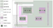
图8示出了基于上述FDSOI标准单元的填充单元的生成方法生成的插入LVT器件和RVT器件的填充单元的版图示意图,如图8所示,本实施例中的填充单元的版图,右半部分被阱识别层覆盖,可以使P型阱/N型阱和SDP区/SDN区相对设置。即,左部区域在中线以上为N型阱和P+离子注入区,中线以下为P型阱和N+离子注入区,因此可与RVT器件正常邻接;右部区域在中线以上为P型阱和N+离子注入区,中线以下为N型阱和P+离子注入区,可与LVT器件正常邻接;中间部分全部为N型阱和P+离子注入区,连接左边部分与右边部分的N型阱和P+离子注入区。图中的设计规则限制是指根据晶圆工厂提供的最小设计规则及二分之一最小规则,保证单元版图自动拼接后可以通过设计规则检查。此结构可应用于左右两侧器件均具有稳定衬底电压的情况。FIG. 8 shows a schematic diagram of the layout of the filled cells inserted into the LVT device and the RVT device generated based on the above-mentioned method for generating the filled cells of the FDSOI standard cell. As shown in FIG. 8 , the layout of the filled cells in this embodiment, the right half Covered by the well discriminating layer, the P-type well/N-type well and the SDP region/SDN region can be disposed opposite to each other. That is, the left region above the center line is the N-type well and the P+ ion implantation region, and below the center line is the P-type well and the N+ ion implantation region, so it can be normally adjacent to the RVT device; the right region is above the center line. P-type well and N+ The ion implantation area, below the center line is the N-type well and the P+ ion implantation area, which can be normally adjacent to the LVT device; the middle part is all N-type well and P+ ion implantation area, connecting the left part and the right part N-type well and P+ ion implantation Area. The design rule restriction in the figure refers to the minimum design rule and one-half minimum rule provided by the wafer factory to ensure that the unit layout can pass the design rule check after automatic splicing. This structure can be applied to the case where both the left and right side devices have stable substrate voltage.
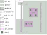
图9示出了基于上述FDSOI结构的版图生成方法生成的另一种插入LVT器件和RVT器件的填充单元的版图示意图,如图9所示,在图8所示的填充单元的结构基础上,根据版图设计基本参数和晶圆工厂提供的设计规则,在满足有源区设计规则的前提下,在基本结构空白区域内画出能够容许的最大的有源区,然后根据接触孔设计规则,在有源区上均匀画出接触孔,使用金属连接到衬底电压源上,达到衬底电压源连接衬底的作用。本实施例提供的结构相较于图8实施例中提供的机构,面积增大,可有效避免插入器件无衬底电位的情况发生。FIG. 9 shows a schematic layout diagram of another filling unit inserted into LVT devices and RVT devices generated by the layout generation method based on the above FDSOI structure. As shown in FIG. 9, on the basis of the structure of the filling unit shown in FIG. 8, According to the basic parameters of layout design and the design rules provided by the wafer factory, on the premise of satisfying the active area design rules, draw the largest allowable active area in the blank area of the basic structure, and then according to the contact hole design rules, Contact holes are drawn uniformly on the active area, and metal is used to connect to the substrate voltage source, so as to achieve the function of connecting the substrate voltage source to the substrate. Compared with the structure provided in the embodiment of FIG. 8 , the structure provided in this embodiment has an increased area, which can effectively avoid the occurrence of the situation where the inserted device has no substrate potential.
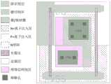
图10示出了基于上述FDSOI标准单元的填充单元的生成方法生成的插入SNW器件和RVT器件的填充单元的版图示意图;图11示出了基于上述FDSOI标准单元的填充单元的生成方法生成的插入SNW器件和LVT器件的填充单元的版图示意图;图12示出了基于上述FDSOI标准单元的填充单元的生成方法生成的插入SPW器件和RVT器件的填充单元的版图示意图;图13示出了基于上述FDSOI标准单元的填充单元的生成方法生成的插入SPW器件和LVT器件的填充单元的版图示意图。FIG. 10 shows a schematic layout diagram of the filled cells inserted into SNW devices and RVT devices generated based on the above-mentioned method for generating filled cells of FDSOI standard cells; FIG. Schematic diagram of the layout of the filled cells of SNW devices and LVT devices; FIG. 12 shows a schematic layout of the filled cells of SPW devices and RVT devices generated based on the above-mentioned generation method of the filled cells of FDSOI standard cells; A schematic diagram of the layout of the filled cells inserted into SPW devices and LVT devices generated by the method for generating filled cells of FDSOI standard cells.
上述实施例中,VPW(Voltage of P-well)为P型阱的顶层金属区,VNW(Voltage ofN-well)为N型阱的顶层金属区。In the above embodiment, VPW (Voltage of P-well) is the top metal region of the P-type well, and VNW (Voltage of N-well) is the top metal region of the N-type well.
显然,上述实施例仅仅是为清楚地说明所作的举例,而并非对实施方式的限定。对于所属领域的普通技术人员来说,在上述说明的基础上还可以做出其它不同形式的变化或变动。这里无需也无法对所有的实施方式予以穷举。而由此所引伸出的显而易见的变化或变动仍处于本申请创造的保护范围之中。Obviously, the above-mentioned embodiments are only examples for clear description, and are not intended to limit the implementation manner. For those of ordinary skill in the art, changes or modifications in other different forms can also be made on the basis of the above description. There is no need and cannot be exhaustive of all implementations here. And the obvious changes or changes derived from this are still within the scope of protection created by the present application.
Claims (7)
Priority Applications (1)
| Application Number | Priority Date | Filing Date | Title |
|---|---|---|---|
| CN201910938131.7ACN110660792B (en) | 2019-09-30 | 2019-09-30 | The generation method and layout layout method of filling pattern of FDSOI standard cell |
Applications Claiming Priority (1)
| Application Number | Priority Date | Filing Date | Title |
|---|---|---|---|
| CN201910938131.7ACN110660792B (en) | 2019-09-30 | 2019-09-30 | The generation method and layout layout method of filling pattern of FDSOI standard cell |
Publications (2)
| Publication Number | Publication Date |
|---|---|
| CN110660792Atrue CN110660792A (en) | 2020-01-07 |
| CN110660792B CN110660792B (en) | 2022-03-18 |
Family
ID=69038606
Family Applications (1)
| Application Number | Title | Priority Date | Filing Date |
|---|---|---|---|
| CN201910938131.7AActiveCN110660792B (en) | 2019-09-30 | 2019-09-30 | The generation method and layout layout method of filling pattern of FDSOI standard cell |
Country Status (1)
| Country | Link |
|---|---|
| CN (1) | CN110660792B (en) |
Cited By (6)
| Publication number | Priority date | Publication date | Assignee | Title |
|---|---|---|---|---|
| CN112380809A (en)* | 2020-11-16 | 2021-02-19 | 成都海光微电子技术有限公司 | Standard unit, physical rule verification method and device of standard unit library and electronic equipment |
| CN112966458A (en)* | 2021-04-07 | 2021-06-15 | 北京华大九天科技股份有限公司 | Graphic processing method, electronic device, server, and storage medium |
| CN113745212A (en)* | 2020-05-29 | 2021-12-03 | 泉芯集成电路制造(济南)有限公司 | Integrated circuit and method for laying out integrated circuit |
| CN114036889A (en)* | 2021-10-29 | 2022-02-11 | 上海华力集成电路制造有限公司 | Layout design method for edge unit of standard cell library |
| CN114358174A (en)* | 2021-12-31 | 2022-04-15 | 海光信息技术股份有限公司 | Standard unit discharge rate test classification method, apparatus, equipment, procedure and medium |
| CN114692549A (en)* | 2022-03-11 | 2022-07-01 | 上海华力集成电路制造有限公司 | Layout Design Method of Filled Cells |
Citations (16)
| Publication number | Priority date | Publication date | Assignee | Title |
|---|---|---|---|---|
| US20050235240A1 (en)* | 2004-04-16 | 2005-10-20 | Taiwan Semiconductor Manufacturing Co., Ltd. | Method for reducing layers revision in engineering change order |
| US20060131609A1 (en)* | 2004-12-17 | 2006-06-22 | Koichi Kinoshita | Semiconductor integrated circuit device formed by automatic layout wiring by use of standard cells and design method of fixing its well potential |
| CN101320707A (en)* | 2008-05-19 | 2008-12-10 | 深圳市国微电子股份有限公司 | Integrated circuit setting and production method especially for structuration |
| WO2009055113A1 (en)* | 2007-10-26 | 2009-04-30 | Synopsys, Inc. | Filler cells for design optimization in a place-and-route system |
| US20100213974A1 (en)* | 2009-02-24 | 2010-08-26 | SypherMedia Interational, Inc., | Method and apparatus for camouflaging a printed circuit board |
| US7797646B2 (en)* | 2005-04-20 | 2010-09-14 | Taiwan Semiconductor Manufacturing Co., Ltd. | Method for using mixed multi-Vt devices in a cell-based design |
| US20100269081A1 (en)* | 2009-04-15 | 2010-10-21 | Taiwan Semiconductor Manufacturing Company, Ltd. | Standard Cells Having Flexible Layout Architecture/Boundaries |
| US20110145775A1 (en)* | 2009-12-11 | 2011-06-16 | Kabushiki Kaisha Toshiba | Cell library, layout method, and layout apparatus |
| US8136072B2 (en)* | 2008-11-03 | 2012-03-13 | Arm Limited | Standard cell placement |
| CN103022032A (en)* | 2012-12-07 | 2013-04-03 | 中国科学院微电子研究所 | Standard cell library layout design method, layout method and standard cell library |
| US8826212B2 (en)* | 2012-12-06 | 2014-09-02 | Taiwan Semiconductor Manufacturing Company, Ltd. | Method of forming a layout including cells having different threshold voltages, a system of implementing and a layout formed |
| US8959472B1 (en)* | 2013-09-27 | 2015-02-17 | Arm Limited | Considering compatibility of adjacent boundary regions for standard cells placement and routing |
| US20160055283A1 (en)* | 2014-08-22 | 2016-02-25 | Samsung Electronics Co., Ltd. | Standard cell library, method of using the same, and method of designing semiconductor integrated circuit |
| US20180151550A1 (en)* | 2016-11-28 | 2018-05-31 | Taiwan Semiconductor Manufacturing Company Limited | Semiconductor Device with Reduced Leakage Current |
| JP2018151977A (en)* | 2017-03-14 | 2018-09-27 | 株式会社リコー | Semiconductor integrated circuit design support apparatus and method |
| CN109977540A (en)* | 2019-03-26 | 2019-07-05 | 上海华力集成电路制造有限公司 | Integrated circuit standard cell library method for building up |
- 2019
- 2019-09-30CNCN201910938131.7Apatent/CN110660792B/enactiveActive
Patent Citations (21)
| Publication number | Priority date | Publication date | Assignee | Title |
|---|---|---|---|---|
| US20050235240A1 (en)* | 2004-04-16 | 2005-10-20 | Taiwan Semiconductor Manufacturing Co., Ltd. | Method for reducing layers revision in engineering change order |
| US20060131609A1 (en)* | 2004-12-17 | 2006-06-22 | Koichi Kinoshita | Semiconductor integrated circuit device formed by automatic layout wiring by use of standard cells and design method of fixing its well potential |
| CN1838411A (en)* | 2004-12-17 | 2006-09-27 | 株式会社东芝 | Semiconductor integrated circuit device and design method for fixing its well potential |
| US7797646B2 (en)* | 2005-04-20 | 2010-09-14 | Taiwan Semiconductor Manufacturing Co., Ltd. | Method for using mixed multi-Vt devices in a cell-based design |
| WO2009055113A1 (en)* | 2007-10-26 | 2009-04-30 | Synopsys, Inc. | Filler cells for design optimization in a place-and-route system |
| US20090113368A1 (en)* | 2007-10-26 | 2009-04-30 | Synopsys, Inc. | Filler cells for design optimization in a place-and-route system |
| CN101681878A (en)* | 2007-10-26 | 2010-03-24 | 新思科技有限公司 | Filler cells for design optimization in a place-and-route system |
| CN101320707A (en)* | 2008-05-19 | 2008-12-10 | 深圳市国微电子股份有限公司 | Integrated circuit setting and production method especially for structuration |
| US8136072B2 (en)* | 2008-11-03 | 2012-03-13 | Arm Limited | Standard cell placement |
| US20100213974A1 (en)* | 2009-02-24 | 2010-08-26 | SypherMedia Interational, Inc., | Method and apparatus for camouflaging a printed circuit board |
| US20100269081A1 (en)* | 2009-04-15 | 2010-10-21 | Taiwan Semiconductor Manufacturing Company, Ltd. | Standard Cells Having Flexible Layout Architecture/Boundaries |
| US20110145775A1 (en)* | 2009-12-11 | 2011-06-16 | Kabushiki Kaisha Toshiba | Cell library, layout method, and layout apparatus |
| US8826212B2 (en)* | 2012-12-06 | 2014-09-02 | Taiwan Semiconductor Manufacturing Company, Ltd. | Method of forming a layout including cells having different threshold voltages, a system of implementing and a layout formed |
| CN103022032A (en)* | 2012-12-07 | 2013-04-03 | 中国科学院微电子研究所 | Standard cell library layout design method, layout method and standard cell library |
| US8959472B1 (en)* | 2013-09-27 | 2015-02-17 | Arm Limited | Considering compatibility of adjacent boundary regions for standard cells placement and routing |
| CN104517004A (en)* | 2013-09-27 | 2015-04-15 | Arm有限公司 | Method of generating an integrated circuit layout |
| US20160055283A1 (en)* | 2014-08-22 | 2016-02-25 | Samsung Electronics Co., Ltd. | Standard cell library, method of using the same, and method of designing semiconductor integrated circuit |
| US20180151550A1 (en)* | 2016-11-28 | 2018-05-31 | Taiwan Semiconductor Manufacturing Company Limited | Semiconductor Device with Reduced Leakage Current |
| CN108122901A (en)* | 2016-11-28 | 2018-06-05 | 台湾积体电路制造股份有限公司 | Integrated circuit with a plurality of transistors |
| JP2018151977A (en)* | 2017-03-14 | 2018-09-27 | 株式会社リコー | Semiconductor integrated circuit design support apparatus and method |
| CN109977540A (en)* | 2019-03-26 | 2019-07-05 | 上海华力集成电路制造有限公司 | Integrated circuit standard cell library method for building up |
Cited By (10)
| Publication number | Priority date | Publication date | Assignee | Title |
|---|---|---|---|---|
| CN113745212A (en)* | 2020-05-29 | 2021-12-03 | 泉芯集成电路制造(济南)有限公司 | Integrated circuit and method for laying out integrated circuit |
| CN112380809A (en)* | 2020-11-16 | 2021-02-19 | 成都海光微电子技术有限公司 | Standard unit, physical rule verification method and device of standard unit library and electronic equipment |
| CN112380809B (en)* | 2020-11-16 | 2021-08-03 | 成都海光微电子技术有限公司 | Standard unit, physical rule verification method, device and equipment of standard unit library |
| CN112966458A (en)* | 2021-04-07 | 2021-06-15 | 北京华大九天科技股份有限公司 | Graphic processing method, electronic device, server, and storage medium |
| CN112966458B (en)* | 2021-04-07 | 2022-07-26 | 北京华大九天科技股份有限公司 | Graphic processing method, electronic device, server, and storage medium |
| CN114036889A (en)* | 2021-10-29 | 2022-02-11 | 上海华力集成电路制造有限公司 | Layout design method for edge unit of standard cell library |
| CN114036889B (en)* | 2021-10-29 | 2025-05-27 | 上海华力集成电路制造有限公司 | Layout Design Method for Edge Cells in Standard Cell Library |
| CN114358174A (en)* | 2021-12-31 | 2022-04-15 | 海光信息技术股份有限公司 | Standard unit discharge rate test classification method, apparatus, equipment, procedure and medium |
| CN114692549A (en)* | 2022-03-11 | 2022-07-01 | 上海华力集成电路制造有限公司 | Layout Design Method of Filled Cells |
| CN114692549B (en)* | 2022-03-11 | 2025-10-03 | 上海华力集成电路制造有限公司 | Layout Design Method for Filling Cells |
Also Published As
| Publication number | Publication date |
|---|---|
| CN110660792B (en) | 2022-03-18 |
Similar Documents
| Publication | Publication Date | Title |
|---|---|---|
| CN110660792A (en) | The generation method and layout layout method of filling pattern of FDSOI standard cell | |
| US12356714B2 (en) | Semiconductor integrated circuit device | |
| US7919792B2 (en) | Standard cell architecture and methods with variable design rules | |
| US9368589B2 (en) | Semiconductor device and semiconductor module | |
| CN102804376B (en) | charging protection device | |
| US11741285B2 (en) | Semiconductor device and method of manufacturing the same | |
| KR101017809B1 (en) | Semiconductor device and manufacturing method thereof | |
| CN105826318B (en) | semiconductor structure | |
| US11705456B2 (en) | Semiconductor device having active fin pattern at cell boundary | |
| KR20170023358A (en) | Semiconductor device | |
| US20080179676A1 (en) | Semiconductor memory device | |
| CN106206586B (en) | Static random access memory | |
| TW201618279A (en) | Semiconductor device and above manufacturing method | |
| US11790146B2 (en) | Semiconductor device | |
| CN105718611A (en) | Layout structure design method for FinFET process standard cell library | |
| KR20120069258A (en) | Vertical memory cell of semiconductor device | |
| WO2014181819A1 (en) | Semiconductor device | |
| US9634008B2 (en) | Semiconductor device and manufacturing method of semiconductor device | |
| US6914300B2 (en) | Semiconductor device | |
| CN106571366B (en) | static random access memory and manufacturing method thereof | |
| CN105826319B (en) | semiconductor structure | |
| CN112786600B (en) | Three-dimensional memory, circuit chip and manufacturing method thereof | |
| CN113506797B (en) | Voltage conversion isolation structure | |
| KR20140086305A (en) | Vertical junctionless semiconductor and method of the same | |
| JP2013045911A (en) | Semiconductor device and manufacturing method of semiconductor device |
Legal Events
| Date | Code | Title | Description |
|---|---|---|---|
| PB01 | Publication | ||
| PB01 | Publication | ||
| SE01 | Entry into force of request for substantive examination | ||
| SE01 | Entry into force of request for substantive examination | ||
| GR01 | Patent grant | ||
| GR01 | Patent grant | ||
| TR01 | Transfer of patent right | Effective date of registration:20250509 Address after:No. 6 Liangteng Road, Pudong New Area, Shanghai, 201317 Patentee after:SHANGHAI HUALI INTEGRATED CIRCUIT MANUFACTURING Co.,Ltd. Country or region after:China Address before:568 Gaosi Road, Pudong New Area pilot Free Trade Zone, Shanghai, 201203 Patentee before:Shanghai Huali Microelectronics Co.,Ltd. Country or region before:China | |
| TR01 | Transfer of patent right |