CN110651455A - Receiver/transmitter co-calibration of voltage levels in a pulse amplitude modulation link - Google Patents
Receiver/transmitter co-calibration of voltage levels in a pulse amplitude modulation linkDownload PDFInfo
- Publication number
- CN110651455A CN110651455ACN201880030308.7ACN201880030308ACN110651455ACN 110651455 ACN110651455 ACN 110651455ACN 201880030308 ACN201880030308 ACN 201880030308ACN 110651455 ACN110651455 ACN 110651455A
- Authority
- CN
- China
- Prior art keywords
- pam
- signal
- distortion
- symbol
- distortion information
- Prior art date
- Legal status (The legal status is an assumption and is not a legal conclusion. Google has not performed a legal analysis and makes no representation as to the accuracy of the status listed.)
- Granted
Links
Images


Classifications
- H—ELECTRICITY
- H04—ELECTRIC COMMUNICATION TECHNIQUE
- H04L—TRANSMISSION OF DIGITAL INFORMATION, e.g. TELEGRAPHIC COMMUNICATION
- H04L25/00—Baseband systems
- H04L25/02—Details ; arrangements for supplying electrical power along data transmission lines
- H04L25/03—Shaping networks in transmitter or receiver, e.g. adaptive shaping networks
- H04L25/03006—Arrangements for removing intersymbol interference
- H04L25/03178—Arrangements involving sequence estimation techniques
- H04L25/03248—Arrangements for operating in conjunction with other apparatus
- H04L25/03254—Operation with other circuitry for removing intersymbol interference
- H04L25/03267—Operation with other circuitry for removing intersymbol interference with decision feedback equalisers
- H—ELECTRICITY
- H04—ELECTRIC COMMUNICATION TECHNIQUE
- H04B—TRANSMISSION
- H04B10/00—Transmission systems employing electromagnetic waves other than radio-waves, e.g. infrared, visible or ultraviolet light, or employing corpuscular radiation, e.g. quantum communication
- H04B10/50—Transmitters
- H04B10/516—Details of coding or modulation
- H04B10/54—Intensity modulation
- H04B10/541—Digital intensity or amplitude modulation
- H—ELECTRICITY
- H04—ELECTRIC COMMUNICATION TECHNIQUE
- H04B—TRANSMISSION
- H04B10/00—Transmission systems employing electromagnetic waves other than radio-waves, e.g. infrared, visible or ultraviolet light, or employing corpuscular radiation, e.g. quantum communication
- H04B10/60—Receivers
- H04B10/66—Non-coherent receivers, e.g. using direct detection
- H04B10/69—Electrical arrangements in the receiver
- H04B10/697—Arrangements for reducing noise and distortion
- H—ELECTRICITY
- H04—ELECTRIC COMMUNICATION TECHNIQUE
- H04L—TRANSMISSION OF DIGITAL INFORMATION, e.g. TELEGRAPHIC COMMUNICATION
- H04L25/00—Baseband systems
- H04L25/02—Details ; arrangements for supplying electrical power along data transmission lines
- H04L25/0264—Arrangements for coupling to transmission lines
- H04L25/028—Arrangements specific to the transmitter end
- H—ELECTRICITY
- H04—ELECTRIC COMMUNICATION TECHNIQUE
- H04L—TRANSMISSION OF DIGITAL INFORMATION, e.g. TELEGRAPHIC COMMUNICATION
- H04L25/00—Baseband systems
- H04L25/02—Details ; arrangements for supplying electrical power along data transmission lines
- H04L25/0264—Arrangements for coupling to transmission lines
- H04L25/0292—Arrangements specific to the receiver end
- H—ELECTRICITY
- H04—ELECTRIC COMMUNICATION TECHNIQUE
- H04L—TRANSMISSION OF DIGITAL INFORMATION, e.g. TELEGRAPHIC COMMUNICATION
- H04L25/00—Baseband systems
- H04L25/02—Details ; arrangements for supplying electrical power along data transmission lines
- H04L25/03—Shaping networks in transmitter or receiver, e.g. adaptive shaping networks
- H04L25/03878—Line equalisers; line build-out devices
- H—ELECTRICITY
- H04—ELECTRIC COMMUNICATION TECHNIQUE
- H04L—TRANSMISSION OF DIGITAL INFORMATION, e.g. TELEGRAPHIC COMMUNICATION
- H04L25/00—Baseband systems
- H04L25/02—Details ; arrangements for supplying electrical power along data transmission lines
- H04L25/06—DC level restoring means; Bias distortion correction ; Decision circuits providing symbol by symbol detection
- H04L25/061—DC level restoring means; Bias distortion correction ; Decision circuits providing symbol by symbol detection providing hard decisions only; arrangements for tracking or suppressing unwanted low frequency components, e.g. removal of DC offset
- H—ELECTRICITY
- H04—ELECTRIC COMMUNICATION TECHNIQUE
- H04L—TRANSMISSION OF DIGITAL INFORMATION, e.g. TELEGRAPHIC COMMUNICATION
- H04L25/00—Baseband systems
- H04L25/38—Synchronous or start-stop systems, e.g. for Baudot code
- H04L25/40—Transmitting circuits; Receiving circuits
- H04L25/49—Transmitting circuits; Receiving circuits using code conversion at the transmitter; using predistortion; using insertion of idle bits for obtaining a desired frequency spectrum; using three or more amplitude levels ; Baseband coding techniques specific to data transmission systems
- H04L25/4917—Transmitting circuits; Receiving circuits using code conversion at the transmitter; using predistortion; using insertion of idle bits for obtaining a desired frequency spectrum; using three or more amplitude levels ; Baseband coding techniques specific to data transmission systems using multilevel codes
- H—ELECTRICITY
- H04—ELECTRIC COMMUNICATION TECHNIQUE
- H04L—TRANSMISSION OF DIGITAL INFORMATION, e.g. TELEGRAPHIC COMMUNICATION
- H04L27/00—Modulated-carrier systems
- H04L27/01—Equalisers
- H—ELECTRICITY
- H04—ELECTRIC COMMUNICATION TECHNIQUE
- H04L—TRANSMISSION OF DIGITAL INFORMATION, e.g. TELEGRAPHIC COMMUNICATION
- H04L27/00—Modulated-carrier systems
- H04L27/02—Amplitude-modulated carrier systems, e.g. using on-off keying; Single sideband or vestigial sideband modulation
- H04L27/04—Modulator circuits; Transmitter circuits
- H—ELECTRICITY
- H04—ELECTRIC COMMUNICATION TECHNIQUE
- H04L—TRANSMISSION OF DIGITAL INFORMATION, e.g. TELEGRAPHIC COMMUNICATION
- H04L27/00—Modulated-carrier systems
- H04L27/02—Amplitude-modulated carrier systems, e.g. using on-off keying; Single sideband or vestigial sideband modulation
- H04L27/06—Demodulator circuits; Receiver circuits
- H—ELECTRICITY
- H04—ELECTRIC COMMUNICATION TECHNIQUE
- H04L—TRANSMISSION OF DIGITAL INFORMATION, e.g. TELEGRAPHIC COMMUNICATION
- H04L27/00—Modulated-carrier systems
- H04L27/02—Amplitude-modulated carrier systems, e.g. using on-off keying; Single sideband or vestigial sideband modulation
- H04L27/08—Amplitude regulation arrangements
- H—ELECTRICITY
- H04—ELECTRIC COMMUNICATION TECHNIQUE
- H04L—TRANSMISSION OF DIGITAL INFORMATION, e.g. TELEGRAPHIC COMMUNICATION
- H04L27/00—Modulated-carrier systems
- H04L27/26—Systems using multi-frequency codes
- H04L27/2601—Multicarrier modulation systems
- H04L27/2647—Arrangements specific to the receiver only
- H04L27/2655—Synchronisation arrangements
- H04L27/2668—Details of algorithms
- H04L27/2673—Details of algorithms characterised by synchronisation parameters
- H04L27/2676—Blind, i.e. without using known symbols
- H04L27/2679—Decision-aided
- H—ELECTRICITY
- H03—ELECTRONIC CIRCUITRY
- H03K—PULSE TECHNIQUE
- H03K7/00—Modulating pulses with a continuously-variable modulating signal
- H03K7/02—Amplitude modulation, i.e. PAM
Landscapes
- Engineering & Computer Science (AREA)
- Computer Networks & Wireless Communication (AREA)
- Signal Processing (AREA)
- Power Engineering (AREA)
- Physics & Mathematics (AREA)
- Electromagnetism (AREA)
- Spectroscopy & Molecular Physics (AREA)
- Dc Digital Transmission (AREA)
Abstract
Description
Translated fromChinese背景技术Background technique
在高速数据传输系统中,脉冲幅度调制(PAM)信令被用于将数据从传输设备承载到接收设备。虽然2级PAM(PAM-2)信令系统本质上是线性的,但是具有多于2级的多级PAM信令系统(PAM-N)可能会遭受非线性失真。发射器和接收器内的不同组件可以在PAM信号中引入PAM目标电平的非相等分布。从多PAM电平的这些不希望的电压偏移可能会影响接收器从信号正确恢复数据的能力。In high-speed data transmission systems, Pulse Amplitude Modulation (PAM) signaling is used to carry data from a transmitting device to a receiving device. While a 2-level PAM (PAM-2) signaling system is linear in nature, a multi-level PAM signaling system (PAM-N) with more than 2 levels may suffer from nonlinear distortion. Different components within the transmitter and receiver can introduce unequal distributions of PAM target levels in the PAM signal. These undesired voltage excursions from multiple PAM levels may affect the receiver's ability to correctly recover data from the signal.
附图说明Description of drawings
通过结合附图考虑以下详细说明可以容易地理解本文的实施例的教导。The teachings of the embodiments herein may be readily understood by considering the following detailed description in conjunction with the accompanying drawings.
图1是根据本公开的实施例的具有示例接收器/发射器校准架构的系统的图示。1 is an illustration of a system with an example receiver/transmitter calibration architecture in accordance with an embodiment of the present disclosure.
图2是根据本公开的实施例的图1的PAM-N接收设备的示例接收器接口电路的图示。2 is an illustration of an example receiver interface circuit of the PAM-N receiving device of FIG. 1 in accordance with an embodiment of the present disclosure.
图3是描绘了根据本公开的实施例的理想PAM-N眼图和具有电平失真的PAM-N眼图的示例波形的图示。3 is a diagram depicting example waveforms of an ideal PAM-N eye diagram and a PAM-N eye diagram with level distortion in accordance with embodiments of the present disclosure.
图4是根据本公开的实施例的图1的PAM-N传输设备的示例驱动器电路的图示。4 is an illustration of an example driver circuit of the PAM-N transmission device of FIG. 1 according to an embodiment of the present disclosure.
图5是根据本公开的实施例的图1的PAM-N接收设备的示例失真检测电路的图示。5 is an illustration of an example distortion detection circuit of the PAM-N receiving device of FIG. 1 according to an embodiment of the present disclosure.
图6图示了根据本公开的实施例的、基于符号间干扰(ISI)的估计来检测PAM-N信号中的失真的示例方法。6 illustrates an example method of detecting distortion in a PAM-N signal based on an estimate of inter-symbol interference (ISI), according to an embodiment of the present disclosure.
图7图示了根据本公开的实施例的基于决策反馈均衡器(DFE)误差电平适配来检测PAM-N信号中的失真的示例方法。7 illustrates an example method for detecting distortion in a PAM-N signal based on decision feedback equalizer (DFE) error level adaptation in accordance with an embodiment of the present disclosure.
图8是图示了根据本公开的实施例的PAM-N链路中的电压电平的接收器/发射器协同校准的方法的示例流程图。8 is an example flow diagram illustrating a method of receiver/transmitter co-calibration of voltage levels in a PAM-N link according to an embodiment of the present disclosure.
具体实施方式Detailed ways
现在将详细参照本公开的若干实施例,其示例在附图中被图示。要注意的是,在可行的情况下,类似或相同的附图标记可以在附图中使用,并且可以指示类似或相同的功能性。这些附图仅出于说明的目的描绘了本公开的实施例。本领域技术人员将从以下描述中容易地识别出,在不脱离本文描述的本公开的原理或所吹捧的益处的情况下,可以采用本文所图示的结构和方法的备选实施例。Reference will now be made in detail to several embodiments of the present disclosure, examples of which are illustrated in the accompanying drawings. It is noted that, where feasible, similar or identical reference numbers may be used in the figures and may indicate similar or identical functionality. These drawings depict embodiments of the present disclosure for purposes of illustration only. Those skilled in the art will readily recognize from the following description that alternative embodiments of the structures and methods illustrated herein may be employed without departing from the principles of the disclosure described herein or the touted benefits.
本公开的实施例涉及一种PAM-N接收设备,包括接收器接口电路,该接收器接口电路用以经由通信信道接收来自PAM-N传输设备的PAM-N信号,其中N大于2,并且PAM-N信号具有针对N个符号的N个信号电平。电路生成失真信息,该失真信息指示与N个信号电平之间的电压差中的不相等相对应的失真级别。驱动器电路向PAM-N传输设备传输指示失真级别的失真信息。Embodiments of the present disclosure relate to a PAM-N receiving device including a receiver interface circuit to receive a PAM-N signal from a PAM-N transmitting device via a communication channel, wherein N is greater than 2 and the PAM -N signal has N signal levels for N symbols. The circuitry generates distortion information indicating levels of distortion corresponding to inequalities in voltage differences between the N signal levels. The driver circuit transmits distortion information indicating the level of distortion to the PAM-N transmission device.
在一个实施例中,PAM-N接收设备进一步包括决策反馈均衡器,其中失真信息是通过以下而被生成:确定第一阈值误差电平,该第一阈值误差电平被用于在以N个符号中的第一符号为目标时生成误差信息,该误差信息用于决策反馈均衡器的抽头权重的适配。确定第二阈值误差电平,该第二阈值误差电平被用于在以N个符号中的第二符号为目标时生成用于误差信息,该误差信息用于决策反馈均衡器的抽头权重的适配,其中失真信息从第一阈值误差电平和第二阈值误差电平被生成。In one embodiment, the PAM-N receiving device further includes a decision feedback equalizer, wherein the distortion information is generated by determining a first threshold error level, the first threshold error level being used in the N number of Error information is generated when the first symbol of the symbols is the target, and the error information is used for adaptation of the tap weights of the decision feedback equalizer. A second threshold error level is determined that is used to generate error information when targeting the second symbol of the N symbols, the error information being used to determine the tap weights of the feedback equalizer adapting, wherein the distortion information is generated from the first threshold error level and the second threshold error level.
在一个实施例中,失真信息是通过以下被生成:在从N个符号中的第一符号转换期间标识第一ISI量。第二ISI量在从N个符号中的第二符号转换期间被标识,其中失真信息从第一ISI量和第二ISI量被生成。In one embodiment, the distortion information is generated by identifying a first ISI amount during conversion from a first symbol of the N symbols. A second ISI amount is identified during conversion from a second of the N symbols, wherein distortion information is generated from the first and second ISI amounts.
在一个实施例中,电路在从第一符号转换到N个符号中的第三符号期间标识第一ISI量。在从第二符号转换到N个符号中的第四符号期间标识第二ISI量。In one embodiment, the circuit identifies the first ISI amount during the transition from the first symbol to the third symbol of the N symbols. A second amount of ISI is identified during the transition from the second symbol to the fourth symbol of the N symbols.
在一个实施例中,电路包括眼扫描电路,该眼扫描电路用以检测针对PAM-N信号的垂直眼开口,其中失真信息从垂直眼开口被生成。In one embodiment, the circuit includes an eye scanning circuit to detect a vertical eye opening for the PAM-N signal, wherein distortion information is generated from the vertical eye opening.
在一个实施例中,电路检测PAM-N信号中何时存在预定图案,并且响应于存在预定图案(predetermined pattern)而生成失真信息。In one embodiment, the circuit detects when a predetermined pattern is present in the PAM-N signal, and generates distortion information in response to the presence of the predetermined pattern.
在一个实施例中,PAM-N接收设备的接收器接口电路包括模拟前端电路,该模拟前端电路将模拟信号调节应用于PAM-N信号。电路生成指示失真级别的失真信息,该失真级别对应于模拟前端电路的输出处的PAM-N信号中的N个信号电平之间的电压差中的不相等。In one embodiment, the receiver interface circuit of the PAM-N receiving device includes an analog front end circuit that applies analog signal conditioning to the PAM-N signal. The circuit generates distortion information indicative of a distortion level corresponding to inequalities in voltage differences between N signal levels in the PAM-N signal at the output of the analog front end circuit.
在一个实施例中,PAM-N传输设备包括驱动器电路,该驱动器电路用以经由通信信道向PAM-N接收设备传输PAM-N信号,其中N大于2,并且PAM-N信号具有与N个符号相对应的N个信号电平。接收器接口电路接收失真信息,该失真信息指示与PAM-N接收设备处的N个信号电平之间的电压差中的不相等相对应的失真级别。驱动器控制电路基于失真信息来调整驱动器电路的一个或多个驱动强度参数。In one embodiment, a PAM-N transmitting device includes a driver circuit to transmit a PAM-N signal to a PAM-N receiving device via a communication channel, wherein N is greater than 2, and the PAM-N signal has N symbols The corresponding N signal levels. The receiver interface circuit receives distortion information indicating distortion levels corresponding to inequalities in voltage differences between the N signal levels at the PAM-N receiving device. The driver control circuit adjusts one or more drive strength parameters of the driver circuit based on the distortion information.
在一个实施例中,PAM-N传输设备的驱动器电路使用预定图案来生成PAM-N信号。In one embodiment, the driver circuit of the PAM-N transmission device uses a predetermined pattern to generate the PAM-N signal.
在一个实施例中,PAM-N传输设备的驱动器电路使用伪随机或加扰图案来生成PAM-N信号。In one embodiment, the driver circuit of the PAM-N transmission device uses a pseudo-random or scrambling pattern to generate the PAM-N signal.
在一个实施例中,PAM-N传输设备的驱动器电路包括与第一符号比特相对应的第一驱动器和与第二符号比特相对应的第二驱动器,其中驱动器控制电路基于失真信息调整一个或多个驱动强度参数,使得第一驱动器的第一驱动强度与第二驱动器的第二驱动强度的比率被调整。In one embodiment, the driver circuit of the PAM-N transmission device includes a first driver corresponding to the first sign bit and a second driver corresponding to the second sign bit, wherein the driver control circuit adjusts one or more of the drivers based on the distortion information a drive strength parameter such that the ratio of the first drive strength of the first driver to the second drive strength of the second driver is adjusted.
在一个实施例中,调整PAM-N传输设备的驱动器控制电路的一个或多个驱动强度参数以最小化电压差的不相等。In one embodiment, one or more drive strength parameters of the driver control circuit of the PAM-N transmission device are adjusted to minimize inequalities in voltage differences.
在一个实施例中,驱动器控制电路调整一个或多个驱动强度参数以匹配驱动器电路的峰值功率约束。In one embodiment, the driver control circuit adjusts one or more drive strength parameters to match the peak power constraints of the driver circuit.
用于PAM-N链路的接收器/发射器协同校准架构Receiver/Transmitter Co-calibration Architecture for PAM-N Links
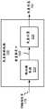
图1是根据本公开的实施例的具有接收器/发射器校准架构100的系统的图示。架构100包括PAM-N传输设备104和PAM-N接收设备154。PAM-N传输设备104可以是集成电路(IC),而PAM-N接收设备154可以是不同的IC。脉冲幅度调制(PAM)可以是信号调制的一种形式,其中数据符号124由PAM-N传输设备104以一系列信号脉冲的幅度进行编码。这是模拟脉冲调制方案,其中,一系列载波脉冲的幅度根据数据符号124的样本值而变化。1 is an illustration of a system having a receiver/transmitter calibration architecture 100 in accordance with an embodiment of the present disclosure. Architecture 100 includes PAM-
通过在每单个时段检测PAM-N信号132的幅度电平来执行解调。PAM-N是指具有N个信号电平的PAM。例如,一些以太网标准使用五级PAM调制(PAM-5),并且一些以太网标准使用具有16个离散级别的PAM(PAM-16)。Demodulation is performed by detecting the amplitude level of the PAM-
PAM-N传输设备104包括驱动器电路128,该驱动器电路128将多比特的数据符号124编码为PAM-N信号132,并且经由通信信道140、通过数据传输线148将PAM-N信号132传输给PAM-N接收设备154,其中N大于2,并且PAM-N信号132具有与N个类型的数据符号相对应的N个信号电平。在一个实施例中,PAM-N信号132是PAM-4信号。PAM-N信号132可以作为差分信号通过数据传输线148被传输(在图1中仅示出了一条线,但是该线可以表示一对线148)。在其他实施例中,PAM-N信号132可以是通过单端导线传输的单端信号。在其他实施例中,PAM-N信号132可以使用不同的编码方案(其中多个比特被编码并且通过多条线被传输)以在差分信号发送与单端信号发送之间进行权衡。PAM-
PAM-N传输设备104包括接收器接口电路108,以经由通信信道140通过数据传输线144接收失真信息162。失真信息162指示由PAM-N接收设备154处的N个信号电平之间的电压差中的不相等所引起的非线性失真的级别。PAM-N传输设备104包括驱动器控制电路116,该驱动器控制电路116接收失真信息162,并且基于失真信息162生成用于调整驱动器电路128的一个或多个驱动强度参数的一个或多个驱动强度控制信号120。PAM-
PAM-N接收设备154包括接收器接口电路172,以经由通信通道140从PAM-N传输设备104接收PAM-N信号132。接收器接口电路172可以是模拟前端(AFE)电路,该模拟前端电路将模拟信号调节应用于PAM-N信号132以在接收器接口电路172的输出处生成PAM-N信号176。将在下面参照图2详细描述接收器接口电路172的示例。The PAM-N receiving device 154 includes
接收器接口电路172的输出处的PAM-N信号176被用作决策电路180的输入,该决策电路180对在PAM-N信号176中所编码的数据符号184做出决策。决策电路180可以包括数据切片器电路,该数据切片器电路将PAM-N信号176的样本与一个或多个决策阈值进行比较。在备选实施例中,模数转换器(ADC)(未示出)可以将PAM-N信号176的模拟电压样本转换为数字样本。然后,数字信号处理器对数字样本进行数字处理,以标识数据符号184。The PAM-
PAM-N接收设备154包括失真检测电路158,以检测由PAM-N信号176的N个信号电平之间的电压差的不相等所引起的非线性失真,并且生成指示失真级别的失真信息162。失真可以在接口电路172的输出处的PAM-N信号176中被检测,该PAM-N信号176是决策电路180的输入。在包括ADC(未示出)的实施例中,失真可以在接口电路172的输出处的PAM-N信号中被检测,该PAM-N信号是ADC的输入。The PAM-N receiving device 154 includes a
PAM-N接收设备154包括驱动器电路166,以向PAM-N传输设备104传输指示失真级别的失真信息162。失真信息162可以在针对物理层通信所预留的分组中被传输。PAM-N传输设备104使用失真信息162来调整驱动器128的驱动强度参数。驱动强度参数被调整,直到PAM-N信号的N个信号电平之间的电压差的不相等被最小化或被消除。因此,可以通过预先调整在传输设备104处的驱动器128的驱动强度来考虑由接收器接口172引入的失真。The PAM-N receiving device 154 includes a
PAM-N接收设备的接收器接口电路Receiver interface circuit of PAM-N receiving equipment
图2是根据本公开的实施例的图1的PAM-N接收设备154的示例接收器接口电路172的图示。接收器接口电路172包括模拟前端(AFE)电路200,该AFE电路200将模拟信号调节应用于PAM-N信号132。AFE电路200的组件可以以非线性方式来操作,这导致PAM-N信号中的N个信号电平之间的电压差中的不相等。上文参照图1图示的失真检测电路158检测失真,该失真对应于AFE电路200的输出处的PAM-N信号176中的N个信号电平之间的电压差中的不相等。FIG. 2 is an illustration of an example
接收器172的AFE 200部分将模拟信号处理应用于PAM-N信号132,以在AFE 200的输出节点处生成PAM-N信号176。AFE 200可以包括具有可变增益的可变增益放大器204,该可变增益放大PAM-N信号132以生成PAM-N信号176。The AFE 200 portion of the
AFE 200可以包括偏移调整电路208,该偏移调整电路208校正AFE 200的各个级的直流(DC)电压偏移以生成用于下一级的合适的PAM-N信号176。AFE 200可以包括连续时间线性均衡器(CTLE)电路212,其对PAM-N信号132应用线性均衡以生成PAM-N信号176。The AFE 200 may include an offset adjustment circuit 208 that corrects the direct current (DC) voltage offset of the various stages of the AFE 200 to generate the appropriate PAM-
可变增益放大器204、偏移调整电路208和CTLE 212的不同配置是可能的,并且CTLE可以被放置在其他两个组件之前或者在信号处理流程的末端。在其他实施例中,AFE200还可以具有其他电路,诸如,离散时间或连续时间前馈均衡(FFE)组件。Different configurations of variable gain amplifier 204, offset adjustment circuit 208, and CTLE 212 are possible, and the CTLE can be placed before the other two components or at the end of the signal processing flow. In other embodiments, AFE 200 may also have other circuits, such as discrete-time or continuous-time feed-forward equalization (FFE) components.
理想的PAM-N眼和具有电平失真的PAM-N眼Ideal PAM-N eye and PAM-N eye with level distortion
图3是描绘了根据本公开的实施例的理想的PAM-N眼图300和具有电平失真的PAM-N眼图350的示例波形的图示。PAM-N眼图300表示示波器显示器,其中来自接收器接口电路172的PAM-N信号176被重复采样并且施加到垂直轴(信号电平304),而数据速率被用于触发水平扫描(时间轴)。它是在特定信令间隔内观察到的感兴趣信号(例如,PAM-N信号176)的不同实现的同步叠加。3 is a diagram depicting example waveforms of an ideal PAM-N eye diagram 300 and a PAM-N eye diagram 350 with level distortion in accordance with embodiments of the present disclosure. The PAM-N eye diagram 300 represents an oscilloscope display in which the PAM-
理想的PAM-N眼300针对信号176的四个符号值00、01、10和11绘制了四个不同的模拟电压电平304。模拟电压电平304中的三个电平差308(在它们上升/下降并且稳定在其稳态电压电平之后)由308A、308B和308C来表示。差异308A表示针对符号值11和10的模拟电压电平之间的电压差。差异308B表示针对符号值10和01的模拟电压电平之间的电压差。差异308C表示针对符号值01和00的模拟电压电平之间的电压差。下面参照图6详细图示和描述信号电平304的示例模拟电压电平。The ideal PAM-N-eye 300 plots four different
在理想情况下,电平差308A、308B和308C彼此相等。如理想的PAM-N眼300所示,电平差308A、电平差308B和电平差308C都等于2V。然而,实际上,驱动器128和/或模拟前端200(以及信道140本身)可以以非线性方式操作,这导致这些电平差308彼此不同。在具有电平失真350的PAM-N眼中图示了这种失真。Ideally, the level differences 308A, 308B and 308C are equal to each other. As shown in an ideal PAM-N eye 300, level difference 308A, level difference 308B, and level difference 308C are all equal to 2V. In practice, however, the
在具有电平失真350的PAM-N眼图中,图示了N个信号电平354之间的模拟电压电平差358中的非线性失真。PAM-N眼图350针对信号176的四个符号值00、01、10和11绘制了四个不同的模拟电压电平354。模拟电压电平354中的三个电平差358由358A、358B和358C表示。差异358A表示针对符号值11和10的模拟电压电平之间的电压差。在这种特定情况下,差异358A小于差异358B,它表示针对符号值10和01的模拟电压电平之间的电压差。差异358C表示针对值01和00的模拟电压电平之间的电压差,并且小于差值358B。三个电平差358彼此不相等,从而在PAM-N眼350中引起失真。In the PAM-N eye diagram with level distortion 350, nonlinear distortion in the analog voltage level difference 358 between N signal levels 354 is illustrated. The PAM-N eye diagram 350 plots four different analog voltage levels 354 for the four
在一个实施例中,接收设备154提供失真信息162,该失真信息162指示与PAM-N信号176中的N个信号电平之间的电压差358中的这些不相等相对应的失真级别。传输设备104然后可以调整驱动器128的驱动强度参数以最小化该失真,使得电压差358更接近理想电压差308。In one embodiment, the receiving device 154 provides
PAM-N传输设备的驱动器电路Driver circuit for PAM-N transmission equipment
图4是根据本公开的实施例的图1的PAM-N传输设备104的示例驱动器电路128的图示。驱动器电路128将数据符号比特转换成可以沿信道140向下传播的电压波形。FIG. 4 is an illustration of an
在PAM-4驱动器的情况下,驱动器电路128可以包括两个差分驱动器400和404。在图4图示的示例驱动器电路中,N的值等于4。可以使用类似于400和404的大量差分驱动器,将驱动器电路类似地设计为更大的N值。去往差分驱动器400的两个差分输入终端是416和420。输入终端416和420承载表示两比特数据符号中的最高有效位(MSB)432的信号。MSB432是具有较大权重的2比特二进制数(例如,01)中的比特位置。来自图1的驱动器控制电路116的驱动强度控制信号120a调整影响差分驱动器400的驱动强度的驱动强度参数。输入终端424和428承载表示两比特数据符号中的最低有效位(LSB)436的信号。LSB 436是具有较小权重的2比特二进制数(例如,01)中的比特位置。来自图1的驱动器控制电路116的驱动强度控制信号120b调整影响差分驱动器404的驱动强度的驱动强度参数。In the case of a PAM-4 driver,
在一个实施例中,差分驱动器400和404可以是电流模式(current mode)驱动器,并且驱动强度控制信号120可以控制其驱动强度。电流图案驱动器通常使用诺顿等效并联终端,并且通常包含在I-V曲线的饱和区域中操作的晶体管。由于高输出共模保持电流源饱和,所以电流图案驱动器用于高性能串行链路,例如,通信信道140。图1所图示的驱动器控制电路116接收失真信息112并且生成两个单独的驱动强度控制信号120a和120b,以用于控制差分驱动器400和404中的电流源的电流。随着驱动强度参数的改变,驱动器控制电路116可以使一个电流源增加其电流,同时使另一电流源减少其电流。这导致差分驱动器400的输出电压改变。In one embodiment, the
在一个实施例中,可以以符合驱动器电路128的峰值功率约束要求的方式来调整驱动器400和404的驱动强度。峰值功率约束规定数据传输系统可以安全消耗的功率量,并且可以影响可靠性。在一些实施例中,峰值功率可以由数据传输线148的峰值额定电压及其特性阻抗来限制。峰值功率约束规范可以包括占空比的长度和平均功率约束。In one embodiment, the drive strengths of
在实施例中,差分驱动器400和404可以是电压图案驱动器,并且驱动强度控制信号120可以控制其驱动强度。电压图案驱动器可以具有多个驱动分段,并且被打开的活动驱动分段的数目确定了驱动器的驱动强度。In an embodiment, the
驱动器400和404的差分输出被组合以生成包括两个互补信号的组合的差分信号132。驱动器400和404的输出被交叉布线,使得组合的差分信号132近似等于正差分输入对(P)减去负差分输入对(N)。The differential outputs of
MSB驱动器400的驱动强度基本上是LSB驱动器404的两倍。可以独立于LSB驱动器404的驱动强度来调整MSB驱动器400的驱动强度。如图3所示,如果在电压差358A、358B、358C之间存在不相等,则可以调整MSB驱动器400的驱动强度与LSB驱动器404的驱动强度之间的比率,以最小化这些不相等。驱动器控制电路116从失真信息162确定如何调整MSB驱动器400与LSB驱动器404的驱动强度的比率。在PAM-4驱动器的情况下,如果失真信息162指示电平差358A和358C(在构造上相等)小于电平差358B,则这意味着在与MSB驱动器400的驱动强度相比时LSB驱动器404的驱动强度不够高。作为结果,驱动器控制电路116可以在减小MSB驱动器400的驱动强度的同时增大LSB驱动器404的驱动强度。相反,如果失真信息162指示电平差358A和358C大于电平差358B,则这意味着在与MSB驱动器400的驱动强度相比时LSB驱动器404的驱动强度太高。作为结果,驱动器控制电路116可以在增大MSB驱动器400的驱动强度的同时减小LSB驱动器404的驱动强度。校正回路可以以“bang-bang”的方式操作,其中在每个步骤中在由失真信息162所指示的方向上施加固定的小校正。The drive strength of the
使用眼扫描的失真检测电路Distortion Detection Circuit Using Eye Scanning
图5是根据本公开的实施例的图1的PAM-N接收设备154的示例失真检测电路158的图示。在该实施例中,眼扫描被用于检测PAM-N信号176中的失真。失真检测电路158包括眼扫描电路504,以检测针对PAM-N信号176的垂直眼开口并且生成描述垂直眼开口的高度的垂直眼开口信息558。如上面参照图3图示和描述的,从垂直眼开口信息558生成失真信息。FIG. 5 is an illustration of an example
图3所示的眼图的内部区域被称为眼开口。在图3的眼图350中存在三个眼开口。失真检测电路158在数据眼图350内的特定时间测量三个眼开口的垂直高度。三个眼开口之间的关系可以等同于电平差358A、358B和358C之间的关系。在一个实施例中,眼扫描电路可以利用比较器确定垂直眼开口,该比较器将PAM-N信号176与参考电压进行比较。参考电压在监测比较器的输出的同时被调整,直到比较器的输出指示数据眼开口的垂直边界被达到。可以针对数据眼350的所有数据眼确定垂直眼开口信息558,或者可以仅针对数据眼的子集确定垂直眼开口信息558,诸如,符号01和10之间的中间数据眼以及符号10与11之间的上数据眼。The inner area of the eye diagram shown in Figure 3 is called the eye opening. There are three eye openings in the eye diagram 350 of FIG. 3 .
失真计算电路508从垂直眼开口信息558计算失真量,然后将该计算结果作为失真信息162输出。例如,可以将上数据眼开口或下数据眼开口(10与11数据线之间或者00与01数据线之间的眼)与中间数据眼开口(01与10数据线之间的眼)进行比较。如果上眼开口或下眼开口大于中间眼开口,则指示电平差358A和358C大于电平差358B。相反,如果上眼开口和下眼开口小于中间眼开口,则指示电平差358A和358C小于电平差358B。该信息作为失真信息162被输出。对于第一阶,上下眼与中眼的比率也与电平差358A和358C与电平差358B的比率相同。该信息也可以被包括在失真信息162中。The
基于ISI检测PAM-N信号中的失真Detection of Distortion in PAM-N Signal Based on ISI
图6图示了根据本公开的实施例的基于符号间干扰(ISI)的估计来检测PAM-N信号176中的失真的示例方法。该方法可以由失真检测电路158执行。ISI是信号176的失真的一种形式,其中一个符号干扰随后的符号,使通信可靠性降低。ISI可能由导致连续符号“模糊”在一起的多径传播或信道的频率响应引起。6 illustrates an example method of detecting distortion in a PAM-
图6图示了数据符号(MSB 432和LSB 436)与PAM-N信号176的理想模拟电压电平304之间的关系。针对符号00,MSB 432为0,LSB 436为0,并且PAM-N信号176的模拟电压电平304理想情况下应为-3V。针对符号01,MSB 432为0,LSB 436为1,并且PAM-N信号176的模拟电压电平理想情况下应为-1V。针对符号10,MSB 432为1,LSB 436为0,并且PAM-N信号176的模拟电压电平304理想情况下应为1V。针对符号11,MSB 432为1,LSB 436为1,并且PAM-N信号176的模拟电压电平304理想情况下应为3V。针对数字值00和01的信号电平304(在图3中由308C表示)理想情况下应该等于(-1--3)V或2V。针对数字值01和10的信号电平304之间的差(在图3中由308B表示)理想情况下应该等于(-1 -1)V或2V。针对数字值10和11的信号电平304之间的差(在图3中由308A表示)理想情况下应该等于(3-1)V或2V。因此,三个电平差308应该彼此相等。当PAM-N信号176中存在非线性失真时,例如,在图3中的眼图350中,三个电平差358彼此不相等。在这种情况下,每个电平差358将不等于2V。FIG. 6 illustrates the relationship between the data symbols (
在图6所图示的实施例中,图1的失真检测电路158通过在从N个符号中的第一符号转换期间标识第一ISI量,并且在从N个符号中的第二符号转换期间标识第二ISI量,来检测由N个信号电平308之间的电压差358的不相等引起的失真,其中从第一ISI量和第二ISI量来生成失真信息。In the embodiment illustrated in FIG. 6 , the
在图6所图示的转换608中,PAM-N信号176在时间616从符号00转换到符号11(第一符号),在时间628转换到符号00(第三符号)。从符号11到符号00的第二次变化是此处感兴趣的转换,尤其是在时间620处。针对符号11的理想信号电平304为3V,并且针对符号00的理想信号电平304为-3V。因此,转换608的理想输出电压摆幅应为(3--3)V或6V。由于来自先前的符号11的ISI,当从符号11转换到符号00时,信号在时间620处经历了第一ISI量624,而不是顺利转换到符号00。In the transition 608 illustrated in FIG. 6 , the PAM-
在转换612中,PAM-N信号176在时间632从符号00转换到符号01(第二符号),在时间644传唤到符号00(第四符号)。从符号01到符号00的第二次变化是此处感兴趣的转换,尤其是在时间640处。针对符号01的理想信号电平304为-1V,并且针对符号00的理想信号电平304为-3V。因此,转换608的理想输出电压摆幅应为(-1--3)V或2V,这是在转换608中经历的电压摆幅的三分之一。由于来自先前的符号01的ISI,当从符号01转换到符号00时,信号在时间640处经历了第二ISI量636,而不是顺利转换到符号00。In transition 612 , the PAM-
失真检测电路158可以从ISI 624的数量与ISI 636的数量的比率来确定信号电平中的失真。从3V处的符号11到-3V处的符号00的转换608确定ISI 624的数量。这表示PAM-N信号电平304中的6V输出电压摆幅。从-1V处的符号01到-3V处的符号00的转换612确定ISI636的数量。这表示PAM-N信号电平304中的2V输出电压摆幅。由于两个转换的电压电平的摆幅之比为6:2或3,因此,第二ISI量636与第一ISI量624之间的比率应该等于1/3。在实施例中,两个原始ISI值可以由失真检测电路158生成。在实施例中,可以由失真检测电路158生成两个数量的ISI的确定比率。在实施例中,确定的ISI比率与理想的ISI比率(1/3)的偏差被输出为失真信息162。
在图6的PAM-4信号的情况下,如果ISI值636小于ISI值624的三分之一,则指示电平差358C小于电平差358B。相反,如果ISI值636大于ISI值624的三分之一,则指示电平差358C大于电平差358B。失真检测电路158可以使用该信息来生成失真信息162。ISI值636和624可以使用DFE误差电平适配外加数据滤波而被计算。数据滤波可以指分析数据决策(例如,数据符号184)以标识目标数据符号序列的存在,然后在存在那些目标数据符号序列时获得ISI值。In the case of the PAM-4 signal of FIG. 6, if the
实际上,基于符号之间的模拟电压差,可以使用第一、第二、第三和第四符号的不同组合来校准接收器/发射器。例如,从10(1V)到00(-3V)的转换(即,输出摆幅为4V)应会经历从01(-1V)到00(-3V)的转换(即,输出摆幅为2V)的ISI的两倍。因此,通过在从N个符号中的第一符号11转换期间标识第一ISI量624,以及在从N个符号中的第二符号01转换期间标识第二ISI量636,来检测失真,其中失真信息从第一ISI量624和第二ISI量636被生成。进一步地,失真检测电路158通过在转换到N个符号中的第三符号00期间标识第一ISI量624,以及在转换到N个符号中的第四个符号00期间标识第二ISI量636,来检测由N个信号电平308之间的电压差358的不相等引起的失真。In practice, different combinations of the first, second, third and fourth symbols can be used to calibrate the receiver/transmitter based on the analog voltage difference between the symbols. For example, a transition from 10 (1V) to 00 (-3V) (i.e., the output swing is 4V) should experience a transition from 01 (-1V) to 00 (-3V) (i.e., the output swing is 2V) twice the ISI. Accordingly, distortion is detected by identifying a
图1的驱动器电路128可以使用专门标识的预定图案来生成PAM-N信号132,以用于在校准接收器/发射器系统中使用。在实施例中,预定图案可以以确认的方式被使用,以验证给定的数字值序列在传输期间产生预期结果。可以通过使用某些转换的重复,或者通过使用伪随机或加扰图案以使用大容量的随机自动测试来生成PAM-N信号132,以集中或系统的方式来产生预定图案。伪随机图案在通过完全确定的因果过程生成时表现出统计随机性。这种方法的益处是比真正的随机图案更容易产生,并且具有可以一次又一次地使用以产生相同结果的益处,这对测试和校准接收器/发射器很有用。在实施例中,可以使用诸如与加扰空闲图案相对应的加扰图案。The
在实施例中,失真检测电路158检测PAM-N信号176中何时存在预定图案,并且响应于存在预定图案来检测由N个信号电平354之间的电压差358的不相等引起的失真。例如,每次失真检测电路158检测到从符号值11到00的转换时,它可以存储所检测到的ISI624的数量。每次失真检测电路158检测到符号值01到00的转换时,它可以存储检测到的ISI 636的数量。在时间间隔上,失真检测电路158响应于预定的转换图案通过聚合ISI值来确定失真量。In an embodiment, the
基于DFE误差电平适配来检测PAM-N信号中的失真Detection of Distortion in PAM-N Signals Based on DFE Error Level Adaptation
图7图示了根据本公开的实施例的基于DFE误差电平适配来检测PAM-N信号中的失真的示例方法。在该实施例中,图1的PAM-N接收设备154包括DFE 700。DFE 700、PAM-N切片器730和求和电路716可以是决策电路180的一部分。DFE是非线性均衡器,其使用检测到的符号184的反馈来产生对信道输出的估计。DFE 700被馈送有所检测到的符号184并且产生输出722、724和726,它们通常从图1的接收电路172的PAM-N输出信号132中被减去。7 illustrates an example method for detecting distortion in a PAM-N signal based on DFE error level adaptation, according to an embodiment of the present disclosure. In this embodiment, the PAM-N receiving device 154 of FIG. 1 includes the DFE 700 . DFE 700 , PAM-
DFE 700包括DFE求和电路716、决策切片器电路730和DFE抽头DAC电路736。DFE抽头DAC电路736包括多个延迟电路,诸如,三个延迟电路702、704和706,以延迟数据符号184。延迟电路702的输出是一个反馈抽头,延迟电路704的输出是另一反馈抽头,并且延迟电路706的输出是另一反馈抽头。DFE 700补偿由先前接收到的数据符号—数据(T1)、数据(T2)和数据(T3)所生成的ISI。每个DFE权重W1、W2和W3是对来自对应抽头的ISI贡献的估计。DFE 700 includes
抽头加权电路742、744和746通过抽头权重W1、W2和W3对每个反馈抽头的延迟数据进行加权,并且输出经加权的反馈信号722、724和726。在一个实施例中,加权电路742、744和746可以是增益可调的数模转换器(DAC),其将每个反馈抽头处的延迟数据转换为模拟电压。求和电路716从PAM-N信号132中减去经加权的反馈信号722、724和726。然后,求和电路716输出由经加权的反馈信号722、724和726与PAM-N信号132的组合产生的决策均衡信号718。
PAM-N决策切片器730对由均衡信号718所表示的数据符号做出决策,从而生成恢复的数据符号184。恢复的数据符号184是PAM-N符号。数据符号184被传递到使用数据符号184的其他电路级(未示出)。在一个实施例中,针对PAM-4符号,PAM-N决策切片器730包括三个单独的切片电路,其将经均衡的信号718与三个单独的决策参考电压进行比较。PAM-
DFE适配引擎172负责实现调谐DFE 700的抽头权重W1、W2、W3的适配算法。DFE适配引擎172可以生成误差参考信号710。误差比较器708将经决策均衡的信号718与误差参考信号710进行比较。误差比较器708输出指示决策均衡信号718的差分电压电平是否大于或小于误差参考信号710的误差信号750。例如,取决于比较,误差信号750可以包括二进制值1或0。误差信号750被传输给DFE适配引擎172,该DFE适配引擎172使用适应算法基于误差信号750来迭代地调整误差参考信号710以及抽头权重W1、W2和W3。DFE适配引擎172还可以在适配过程期间接收和使用数据符号184并使用。The
在DFE误差电平适配期间,通常通过一次以一个符号(例如,10、11)为目标、然后在以该符号为目标的同时将误差参考信号710调整到阈值误差电平,来设置误差参考信号710。DFE误差电平适配过程通常导致误差参考信号710被设置为接近数据眼的边缘的阈值误差电平。例如,参照图3的数据眼图350,当以“11”符号为目标时,误差参考信号710可以被设置为3伏,当以“10”符号为目标时可以被设置为1伏,当以“01”符号为目标时可以被设置为-1伏,以及当以“00”符号为目标时可以被设置为-3伏。During DFE error level adaptation, the error reference is typically set by targeting one symbol at a time (eg, 10, 11) and then adjusting the
误差参考信号710也由DFE适配引擎172传输到失真检测电路158,该失真检测电路158生成失真信息162。
失真检测电路158通过确定误差参考信号710的第一阈值误差电平来生成失真信息162,误差参考信号710被用于生成误差信息750,误差信息750用于在以N个符号中的第一符号(例如,数字值11)为目标时适配DFE 700的抽头权重W1、W2和W3。失真检测电路158确定误差参考信号710的第二阈值误差电平,误差信号710被被用于生成误差信息750,误差信息750用于在以N个符号中的第二符号(例如,10)为目标时适配DFE 700的抽头权重W1、W2和W3。用于DFE误差电平适配的误差电平与电平差358A、358B和358C被相关,并且可以被用作对与电压差的不相等相对应的失真的指示。例如,在理想情况下,以“11”符号为目标时的误差电平应该是以“10”符号为目标时的误差电平的三倍。然而,如果存在失真,如图3的数据眼图350所示,那么两个误差电平将不会是彼此的三倍。
失真信息162从第一阈值误差电平和第二阈值误差电平被生成。在一个实施例中,失真信息162可以通过计算针对“11”符号的阈值误差电平与针对“10”符号的阈值误差电平的比率而被生成。如果针对“11”符号的阈值误差电平与针对“10”信号的阈值误差电平的比率大于3,则指示电平差358A大于电平差358B。相反,如果针对“11”符号的阈值误差电平与针对“10”信号的阈值误差电平的比率小于3,则指示电平差358A小于电平差358B。该信息被用于输出失真信息162。针对其他符号的误差电平可以被用于获得关于三个电平差358A、358B和358C的信息。在传统的DFE误差电平适配过程中,结合适当的数据滤波,获得误差电平。
在PAM-N链路中电压电平的接收器/发射器协同校准的方法Method for Receiver/Transmitter Co-calibration of Voltage Levels in PAM-N Links
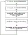
图8是图示了根据本公开的实施例的PAM-N链路中的电压电平的接收器/发射器协同校准的方法的示例流程图。在一些实施例中,该过程可以具有与结合图8所描述的那些步骤不同和/或附加的步骤。可以以与结合图8所描述的顺序不同的顺序来执行处理的步骤。一些步骤可以并行执行。备选地,一些步骤可以被并行执行,并且一些步骤按顺序执行。备选地,一些步骤可以以流水线的方式执行,使得步骤的执行在先前步骤的执行之前开始。8 is an example flow diagram illustrating a method of receiver/transmitter co-calibration of voltage levels in a PAM-N link according to an embodiment of the present disclosure. In some embodiments, the process may have different and/or additional steps than those described in connection with FIG. 8 . The steps of the process may be performed in a different order than that described in connection with FIG. 8 . Some steps can be performed in parallel. Alternatively, some steps may be performed in parallel and some steps are performed sequentially. Alternatively, some steps may be performed in a pipelined fashion, such that execution of steps begins before execution of previous steps.
图1的PAM-N传输设备104经由驱动器电路128、经由通信信道140传输PAM-N信号132(800)。此处,N大于2,并且PAM-N132信号具有与N个符号(例如,000、001、010等)相对应的N个信号电平。PAM-N接收设备经由接收器接口电路172接收PAM-N信号176(在由AFE 200进行电压偏移校正等之后)(804)。失真检测电路158检测非线性失真,该非线性失真对应于PAM-N信号176内的N个信号电平354之间的电压差358的不相等,并且生成指示失真级别的失真信息(808)。The PAM-
PAM-N接收设备154经由驱动器电路166向PAM-N传输设备104传输指示失真级别的失真信息162(812)。PAM-N传输设备104经由接收器接口电路108接收失真信息162。PAM-N传输设备104基于失真信息112、经由驱动器控制电路116来调整PAM-N传输设备104的驱动器电路128的一个或多个驱动强度参数(816)。PAM-N receiving device 154 transmits
在一个实施例中,接收器/发射器校准架构内的电路的表示可以作为数据被存储在非暂时性计算机可读介质(例如,硬盘驱动器、闪存驱动器、光盘驱动器)中。这些表示可以采取例如行为级描述、寄存器传输级描述、逻辑组件级描述、晶体管级描述或布局几何级描述的形式。In one embodiment, a representation of the circuitry within the receiver/transmitter calibration architecture may be stored as data in a non-transitory computer readable medium (eg, hard drive, flash drive, optical drive). These representations may take the form of, for example, behavior-level descriptions, register transfer-level descriptions, logic component-level descriptions, transistor-level descriptions, or layout geometry-level descriptions.
在阅读本公开时,本领域技术人员可以了解包括PAM-N传输设备和PAM-N接收设备的系统的附加备选设计。因此,尽管已经图示和描述了本公开的特定实施例和应用,但是要理解,本公开不限于本文公开的精确构造和组件。在不脱离所附权利要求所定义的本发明的精神和范围的情况下,在本文中可以对本公开的方法和装置的布置、操作和细节进行对本领域技术人员来说可能显而易见的各种修改、改变和变型。Upon reading this disclosure, those skilled in the art can appreciate additional alternative designs for systems including PAM-N transmission devices and PAM-N reception devices. Therefore, while specific embodiments and applications of the present disclosure have been illustrated and described, it is to be understood that the present disclosure is not limited to the precise constructions and components disclosed herein. Various modifications, which may be apparent to those skilled in the art, may be made herein in the arrangement, operation and details of the methods and apparatus of the present disclosure without departing from the spirit and scope of the invention as defined by the appended claims. Alterations and variants.
Claims (20)
Translated fromChineseApplications Claiming Priority (3)
| Application Number | Priority Date | Filing Date | Title |
|---|---|---|---|
| US201762542149P | 2017-08-07 | 2017-08-07 | |
| US62/542,149 | 2017-08-07 | ||
| PCT/US2018/045046WO2019032379A1 (en) | 2017-08-07 | 2018-08-02 | Receiver/transmiter co-calibration of voltage levels in pulse amplitude modulation links |
Publications (2)
| Publication Number | Publication Date |
|---|---|
| CN110651455Atrue CN110651455A (en) | 2020-01-03 |
| CN110651455B CN110651455B (en) | 2023-08-29 |
Family
ID=65271377
Family Applications (1)
| Application Number | Title | Priority Date | Filing Date |
|---|---|---|---|
| CN201880030308.7AExpired - Fee RelatedCN110651455B (en) | 2017-08-07 | 2018-08-02 | Apparatus and method for collaborative calibration of voltage levels in pulse amplitude modulation links |
Country Status (4)
| Country | Link |
|---|---|
| US (3) | US10892920B2 (en) |
| EP (1) | EP3665881A4 (en) |
| CN (1) | CN110651455B (en) |
| WO (1) | WO2019032379A1 (en) |
Cited By (3)
| Publication number | Priority date | Publication date | Assignee | Title |
|---|---|---|---|---|
| CN113726327A (en)* | 2020-05-21 | 2021-11-30 | 爱思开海力士有限公司 | Signal receiver and method for measuring signal receiver offset |
| CN113973034A (en)* | 2020-07-24 | 2022-01-25 | Lg电子株式会社 | Signal receiving apparatus and signal processing method thereof |
| CN115964906A (en)* | 2023-03-17 | 2023-04-14 | 巨霖科技(上海)有限公司 | PAM3 differential port statistical eye pattern simulation method and device based on multi-edge response |
Families Citing this family (10)
| Publication number | Priority date | Publication date | Assignee | Title |
|---|---|---|---|---|
| US10892920B2 (en)* | 2017-08-07 | 2021-01-12 | Rambus Inc. | Receiver/transmitter co-calibration of voltage levels in pulse amplitude modulation links |
| WO2021076800A1 (en)* | 2019-10-15 | 2021-04-22 | Macom Technology Solutions Holdings, Inc. | Finding the eye center with a low-power eye monitor using a 3-dimensional algorithm |
| US11595064B2 (en)* | 2020-08-13 | 2023-02-28 | Texas Instruments Incorporated | Clock recovery and cable diagnostics for ethernet phy |
| US12021668B2 (en) | 2020-12-28 | 2024-06-25 | Micron Technology, Inc. | Equalization for pulse-amplitude modulation |
| KR20220108265A (en) | 2021-01-26 | 2022-08-03 | 삼성전자주식회사 | High bandwidth memory system using multi-level signaling |
| WO2022169996A1 (en)* | 2021-02-03 | 2022-08-11 | Tektronix, Inc. | Eye classes separator with overlay, and composite and dynamic eye-trigger for humans and machine learning |
| TWI774314B (en)* | 2021-04-08 | 2022-08-11 | 新唐科技股份有限公司 | Microcontroller and signal modulation method |
| CN113267914B (en)* | 2021-05-31 | 2022-05-20 | 华中科技大学 | Electro-optic modulator closed-loop nonlinear compensation system based on eye pattern monitoring |
| KR102583000B1 (en)* | 2021-12-10 | 2023-09-25 | 서울시립대학교 산학협력단 | Pam-n receiver capable of adaptively adjusting threshold voltages determining data level of received signal and method of adaptively adjusting threshold voltages thereof |
| US12413455B2 (en)* | 2023-09-11 | 2025-09-09 | Samsung Electronics Co., Ltd. | Adaptive AFE calibration techniques |
Citations (3)
| Publication number | Priority date | Publication date | Assignee | Title |
|---|---|---|---|---|
| US20130094561A1 (en)* | 2011-10-18 | 2013-04-18 | Transwitch Corporation | Techniques for adaptively adjusting decision levels of a pam-n decision feedback equalizer |
| CN104024873A (en)* | 2012-12-13 | 2014-09-03 | 英特尔公司 | Distortion measurement for limiting jitter in pam transmitters |
| US9559880B1 (en)* | 2016-03-04 | 2017-01-31 | Inphi Corporation | Eye modulation for pulse-amplitude modulation communication systems |
Family Cites Families (13)
| Publication number | Priority date | Publication date | Assignee | Title |
|---|---|---|---|---|
| KR100226504B1 (en)* | 1997-07-22 | 1999-10-15 | 김영환 | Data transmission method and apparatus therefor in PAM communication system |
| US6396329B1 (en)* | 1999-10-19 | 2002-05-28 | Rambus, Inc | Method and apparatus for receiving high speed signals with low latency |
| US7233164B2 (en) | 2003-12-17 | 2007-06-19 | Rambus Inc. | Offset cancellation in a multi-level signaling system |
| EP2375662B1 (en)* | 2005-01-20 | 2018-09-26 | Rambus Inc. | High-speed signaling systems with adaptable pre-emphasis and equalization |
| US8804809B2 (en)* | 2011-09-12 | 2014-08-12 | Transwitch Corporation | Techniques for setting feedback coefficients of a PAM-N decision feedback equalizer |
| US8750406B2 (en)* | 2012-01-31 | 2014-06-10 | Altera Corporation | Multi-level amplitude signaling receiver |
| US8923382B2 (en)* | 2012-03-16 | 2014-12-30 | Lsi Corporation | Tap adaptation with a fully unrolled decision feedback equalizer |
| CN104247356B (en)* | 2012-04-19 | 2017-02-22 | 松下知识产权经营株式会社 | Multilevel-signal sending device, multilevel-signal receiving device, multilevel-signal transmission system and multilevel-signal transmission method |
| US8964818B2 (en) | 2012-11-30 | 2015-02-24 | Broadcom Corporation | Use of multi-level modulation signaling for short reach data communications |
| US8989300B1 (en) | 2013-09-06 | 2015-03-24 | Avago Technologies General Ip (Singapore) Pte. Ltd. | Multi-level coding and distortion compensation |
| US10516427B2 (en)* | 2015-10-15 | 2019-12-24 | Rambus Inc. | PAM-4 DFE architectures with symbol-transition dependent DFE tap values |
| US10892920B2 (en)* | 2017-08-07 | 2021-01-12 | Rambus Inc. | Receiver/transmitter co-calibration of voltage levels in pulse amplitude modulation links |
| US10447510B1 (en)* | 2019-02-04 | 2019-10-15 | Globalfoundries Inc. | On-demand feed forward equalizer with distributed arithmetic architecture and method |
- 2018
- 2018-08-02USUS16/611,472patent/US10892920B2/enactiveActive
- 2018-08-02CNCN201880030308.7Apatent/CN110651455B/ennot_activeExpired - Fee Related
- 2018-08-02EPEP18844307.1Apatent/EP3665881A4/ennot_activeWithdrawn
- 2018-08-02WOPCT/US2018/045046patent/WO2019032379A1/ennot_activeCeased
- 2020
- 2020-12-09USUS17/116,460patent/US11323297B2/enactiveActive
- 2022
- 2022-04-01USUS17/711,328patent/US11711246B2/enactiveActive
Patent Citations (3)
| Publication number | Priority date | Publication date | Assignee | Title |
|---|---|---|---|---|
| US20130094561A1 (en)* | 2011-10-18 | 2013-04-18 | Transwitch Corporation | Techniques for adaptively adjusting decision levels of a pam-n decision feedback equalizer |
| CN104024873A (en)* | 2012-12-13 | 2014-09-03 | 英特尔公司 | Distortion measurement for limiting jitter in pam transmitters |
| US9559880B1 (en)* | 2016-03-04 | 2017-01-31 | Inphi Corporation | Eye modulation for pulse-amplitude modulation communication systems |
Cited By (5)
| Publication number | Priority date | Publication date | Assignee | Title |
|---|---|---|---|---|
| CN113726327A (en)* | 2020-05-21 | 2021-11-30 | 爱思开海力士有限公司 | Signal receiver and method for measuring signal receiver offset |
| CN113726327B (en)* | 2020-05-21 | 2023-07-21 | 爱思开海力士有限公司 | Signal receiver and method of measuring signal receiver offset |
| CN113973034A (en)* | 2020-07-24 | 2022-01-25 | Lg电子株式会社 | Signal receiving apparatus and signal processing method thereof |
| CN113973034B (en)* | 2020-07-24 | 2024-05-24 | Lg电子株式会社 | Signal receiving apparatus and signal processing method thereof |
| CN115964906A (en)* | 2023-03-17 | 2023-04-14 | 巨霖科技(上海)有限公司 | PAM3 differential port statistical eye pattern simulation method and device based on multi-edge response |
Also Published As
| Publication number | Publication date |
|---|---|
| US10892920B2 (en) | 2021-01-12 |
| US11323297B2 (en) | 2022-05-03 |
| US20220286329A1 (en) | 2022-09-08 |
| EP3665881A4 (en) | 2021-04-21 |
| EP3665881A1 (en) | 2020-06-17 |
| US20200145261A1 (en) | 2020-05-07 |
| WO2019032379A1 (en) | 2019-02-14 |
| US11711246B2 (en) | 2023-07-25 |
| US20210144031A1 (en) | 2021-05-13 |
| CN110651455B (en) | 2023-08-29 |
Similar Documents
| Publication | Publication Date | Title |
|---|---|---|
| US11711246B2 (en) | Receiver/transmitter co-calibration of voltage levels in pulse amplitude modulation links | |
| US10038575B1 (en) | Decision feedback equalizer with post-cursor non-linearity correction | |
| US12034572B2 (en) | Decision feedback equalization embedded in slicer | |
| US9742422B2 (en) | Receiver with adjustable reference voltages | |
| US8929497B2 (en) | Dynamic deskew for bang-bang timing recovery in a communication system | |
| US8923382B2 (en) | Tap adaptation with a fully unrolled decision feedback equalizer | |
| US8027409B2 (en) | Noise prediction-based signal detection and cross-talk mitigation | |
| US10972319B2 (en) | Clockless decision feedback equalization (DFE) for multi-level signals | |
| US20150085914A1 (en) | Modal PAM2/4 Pipelined Programmable Receiver Having Feed Forward Equalizer (FFE) And Decision Feedback Equalizer (DFE) Optimized For Forward Error Correction (FEC) Bit Error Rate (BER) Performance | |
| US20130243107A1 (en) | Baud rate timing recovery for nyquist patterns in a communication system | |
| US10027516B2 (en) | Receiver with offset calibration | |
| JP2023547774A (en) | Nonlinear neural network equalizer for high-speed data channels | |
| CN111525935B (en) | Receivers for high-speed communication channels | |
| US11888654B2 (en) | Offset detector circuit for differential signal generator, receiver, and method of compensating for offset of differential signal generator | |
| US10103743B1 (en) | Analog-to-digital converter and control method thereof | |
| CN117459203A (en) | Retimer with limiter level adjustment | |
| WO2009003129A2 (en) | Methods and circuits for adaptive equalization and channel characterization using live data | |
| US8693532B2 (en) | Communications with adaptive equalization | |
| US9595990B1 (en) | Circuit for and method of enabling the adaptation of an automatic gain control circuit | |
| US8559495B2 (en) | Equalizer adaptation | |
| JP2024011060A (en) | Receiving circuit for multilevel pam (pulse amplitude modulation) signal and adjustment method thereof |
Legal Events
| Date | Code | Title | Description |
|---|---|---|---|
| PB01 | Publication | ||
| PB01 | Publication | ||
| SE01 | Entry into force of request for substantive examination | ||
| SE01 | Entry into force of request for substantive examination | ||
| GR01 | Patent grant | ||
| GR01 | Patent grant | ||
| CF01 | Termination of patent right due to non-payment of annual fee | ||
| CF01 | Termination of patent right due to non-payment of annual fee | Granted publication date:20230829 |