CN110649356A - Power distribution network, LCD antenna and communication equipment - Google Patents
Power distribution network, LCD antenna and communication equipmentDownload PDFInfo
- Publication number
- CN110649356A CN110649356ACN201810676301.4ACN201810676301ACN110649356ACN 110649356 ACN110649356 ACN 110649356ACN 201810676301 ACN201810676301 ACN 201810676301ACN 110649356 ACN110649356 ACN 110649356A
- Authority
- CN
- China
- Prior art keywords
- liquid crystal
- transmission medium
- microstrip line
- region
- substrate
- Prior art date
- Legal status (The legal status is an assumption and is not a legal conclusion. Google has not performed a legal analysis and makes no representation as to the accuracy of the status listed.)
- Pending
Links
Images


Classifications
- H—ELECTRICITY
- H01—ELECTRIC ELEMENTS
- H01Q—ANTENNAS, i.e. RADIO AERIALS
- H01Q21/00—Antenna arrays or systems
- H01Q21/0006—Particular feeding systems
- H01Q21/0075—Stripline fed arrays
- H—ELECTRICITY
- H01—ELECTRIC ELEMENTS
- H01P—WAVEGUIDES; RESONATORS, LINES, OR OTHER DEVICES OF THE WAVEGUIDE TYPE
- H01P5/00—Coupling devices of the waveguide type
- H01P5/12—Coupling devices having more than two ports
- H—ELECTRICITY
- H01—ELECTRIC ELEMENTS
- H01P—WAVEGUIDES; RESONATORS, LINES, OR OTHER DEVICES OF THE WAVEGUIDE TYPE
- H01P1/00—Auxiliary devices
- H01P1/18—Phase-shifters
- H01P1/182—Waveguide phase-shifters
- H—ELECTRICITY
- H01—ELECTRIC ELEMENTS
- H01Q—ANTENNAS, i.e. RADIO AERIALS
- H01Q1/00—Details of, or arrangements associated with, antennas
- H01Q1/36—Structural form of radiating elements, e.g. cone, spiral, umbrella; Particular materials used therewith
- H01Q1/364—Structural form of radiating elements, e.g. cone, spiral, umbrella; Particular materials used therewith using a particular conducting material, e.g. superconductor
- H—ELECTRICITY
- H01—ELECTRIC ELEMENTS
- H01Q—ANTENNAS, i.e. RADIO AERIALS
- H01Q1/00—Details of, or arrangements associated with, antennas
- H01Q1/36—Structural form of radiating elements, e.g. cone, spiral, umbrella; Particular materials used therewith
- H01Q1/38—Structural form of radiating elements, e.g. cone, spiral, umbrella; Particular materials used therewith formed by a conductive layer on an insulating support
- H—ELECTRICITY
- H01—ELECTRIC ELEMENTS
- H01Q—ANTENNAS, i.e. RADIO AERIALS
- H01Q21/00—Antenna arrays or systems
- H01Q21/06—Arrays of individually energised antenna units similarly polarised and spaced apart
- H01Q21/061—Two dimensional planar arrays
- H01Q21/064—Two dimensional planar arrays using horn or slot aerials
- H—ELECTRICITY
- H01—ELECTRIC ELEMENTS
- H01Q—ANTENNAS, i.e. RADIO AERIALS
- H01Q21/00—Antenna arrays or systems
- H01Q21/06—Arrays of individually energised antenna units similarly polarised and spaced apart
- H01Q21/061—Two dimensional planar arrays
- H01Q21/065—Patch antenna array
- H—ELECTRICITY
- H01—ELECTRIC ELEMENTS
- H01Q—ANTENNAS, i.e. RADIO AERIALS
- H01Q23/00—Antennas with active circuits or circuit elements integrated within them or attached to them
- H—ELECTRICITY
- H01—ELECTRIC ELEMENTS
- H01Q—ANTENNAS, i.e. RADIO AERIALS
- H01Q3/00—Arrangements for changing or varying the orientation or the shape of the directional pattern of the waves radiated from an antenna or antenna system
- H01Q3/26—Arrangements for changing or varying the orientation or the shape of the directional pattern of the waves radiated from an antenna or antenna system varying the relative phase or relative amplitude of energisation between two or more active radiating elements; varying the distribution of energy across a radiating aperture
- H01Q3/30—Arrangements for changing or varying the orientation or the shape of the directional pattern of the waves radiated from an antenna or antenna system varying the relative phase or relative amplitude of energisation between two or more active radiating elements; varying the distribution of energy across a radiating aperture varying the relative phase between the radiating elements of an array
- H01Q3/34—Arrangements for changing or varying the orientation or the shape of the directional pattern of the waves radiated from an antenna or antenna system varying the relative phase or relative amplitude of energisation between two or more active radiating elements; varying the distribution of energy across a radiating aperture varying the relative phase between the radiating elements of an array by electrical means
- H01Q3/36—Arrangements for changing or varying the orientation or the shape of the directional pattern of the waves radiated from an antenna or antenna system varying the relative phase or relative amplitude of energisation between two or more active radiating elements; varying the distribution of energy across a radiating aperture varying the relative phase between the radiating elements of an array by electrical means with variable phase-shifters
Landscapes
- Variable-Direction Aerials And Aerial Arrays (AREA)
- Waveguide Switches, Polarizers, And Phase Shifters (AREA)
Abstract
Translated fromChinese
Description
Translated fromChinese技术领域technical field
本发明一般涉及通信技术领域。更具体地,本发明涉及一种功率分配网络、包括该功率分配网络的液晶天线,以及采用该液晶天线的通信设备。The present invention generally relates to the field of communications technology. More particularly, the present invention relates to a power distribution network, a liquid crystal antenna including the power distribution network, and a communication device employing the liquid crystal antenna.
背景技术Background technique
在典型的液晶阵列天线系统中,功率分配网络通过一分二的功率分配器级联方式将输入功率平均分配给多路输出端口。通常要求功率分配网络在不对其他结构的连续性造成破坏或者是造成较小的影响下,完成对阵元馈电。功率分配器按照结构的不同可以划分成微带结构功率分配器和腔体功率分配器两类。在液晶阵列天线中,通常采用微带结构功率分配器。与腔体功率分配器相比,微带结构功率分配器的隔离度较大,并且集成度较高,但是插入损耗较大。因此,在本领域中存在对于适用于高效率的液晶天线的低损耗功率分配网络的需要。In a typical liquid crystal array antenna system, the power distribution network evenly distributes the input power to the multiple output ports through a cascade of two power dividers. Usually, the power distribution network is required to complete the cell feeding without causing damage to the continuity of other structures or causing a small impact. Power dividers can be divided into microstrip structure power dividers and cavity power dividers according to different structures. In a liquid crystal array antenna, a power divider with a microstrip structure is usually used. Compared with cavity power dividers, microstrip power dividers have higher isolation and higher integration, but larger insertion loss. Therefore, there is a need in the art for a low loss power distribution network suitable for high efficiency liquid crystal antennas.
发明内容SUMMARY OF THE INVENTION
有鉴于此,本发明的一方面提供了一种功率分配网络,所述功率分配网络被配置成使用在液晶天线中,并且包括:多个级联的功率分配器,每一个功率分配器包括第一微带线、传输介质区和参考电极,其中所述传输介质区中的传输介质的介质损耗角的正切值小于所述液晶天线中的液晶的介质损耗角的正切值。In view of this, an aspect of the present invention provides a power distribution network, the power distribution network is configured to be used in a liquid crystal antenna, and includes: a plurality of cascaded power dividers, each power divider includes a first power divider A microstrip line, a transmission medium region and a reference electrode, wherein the tangent of the dielectric loss angle of the transmission medium in the transmission medium region is smaller than the tangent of the dielectric loss angle of the liquid crystal in the liquid crystal antenna.
根据本发明的一些实施例,第一微带线包括多个不同阻抗的微带线,并且每一个功率分配器还包括电耦接在不同阻抗的第一微带线之间的第一阻抗变换器。According to some embodiments of the present invention, the first microstrip line includes a plurality of microstrip lines of different impedances, and each power divider further includes a first impedance transformation electrically coupled between the first microstrip lines of different impedances device.
根据本发明的一些实施例,传输介质区中的传输介质为空气。According to some embodiments of the invention, the transport medium in the transport medium zone is air.
根据本发明的一些实施例,第一微带线的宽度满足下式:According to some embodiments of the present invention, the width of the first microstrip line satisfies the following formula:

其中,


本发明的另一方面提供了一种液晶天线。该液晶天线包括相对设置的第一基板和第二基板;设置在第一基板远离第二基板的一侧的多个辐射元件;上述任一种功率分配网络,功率分配网络配置成向所述多个辐射元件馈送电磁信号;以及移相器。移相器包括:设置在第一基板与第二基板之间的多个液晶区,设置在第一基板与所述多个液晶区之间的参考电极,以及设置在第二基板与所述多个液晶区之间的第二微带线。所述多个液晶区与所述多个辐射元件一一对应,并且每一个辐射元件与对应的液晶区在第二基板上的正投影至少部分重叠。每一个功率分配器的传输介质区设置在相邻液晶区之间,每一个功率分配器的参考电极设置在第一基板与传输介质区之间,并且每一个功率分配器的第一微带线设置在第二基板与传输介质区之间。每一个功率分配器的传输介质区中的传输介质的介质损耗角的正切值小于液晶区中的液晶的介质损耗角的正切值。Another aspect of the present invention provides a liquid crystal antenna. The liquid crystal antenna includes a first substrate and a second substrate arranged oppositely; a plurality of radiating elements arranged on a side of the first substrate away from the second substrate; any of the above-mentioned power distribution networks, the power distribution network is configured to extend to the plurality of radiating elements. a radiating element feeds an electromagnetic signal; and a phase shifter. The phase shifter includes a plurality of liquid crystal regions arranged between the first substrate and the second substrate, a reference electrode arranged between the first substrate and the plurality of liquid crystal regions, and a plurality of liquid crystal regions arranged between the second substrate and the plurality of liquid crystal regions. a second microstrip line between the liquid crystal regions. The plurality of liquid crystal regions are in one-to-one correspondence with the plurality of radiation elements, and each radiation element at least partially overlaps with the orthographic projection of the corresponding liquid crystal region on the second substrate. The transmission medium region of each power divider is disposed between adjacent liquid crystal regions, the reference electrode of each power divider is disposed between the first substrate and the transmission medium region, and the first microstrip line of each power divider arranged between the second substrate and the transmission medium region. The tangent of the dielectric loss angle of the transmission medium in the transmission medium region of each power divider is smaller than the tangent of the dielectric loss angle of the liquid crystal in the liquid crystal region.
根据本发明的一些实施例,传输介质区与相邻的液晶区通过挡墙分离。According to some embodiments of the present invention, the transmission medium region is separated from the adjacent liquid crystal region by a barrier wall.
根据本发明的一些实施例,挡墙由封框胶制成。According to some embodiments of the present invention, the retaining wall is made of frame sealant.
根据本发明的一些实施例,上述液晶天线还包括电耦接在相邻的第一微带线和第二微带线之间的第二阻抗变换器。According to some embodiments of the present invention, the above-mentioned liquid crystal antenna further includes a second impedance transformer electrically coupled between the adjacent first microstrip line and the second microstrip line.
根据本发明的一些实施例,第二微带线的宽度满足下式:According to some embodiments of the present invention, the width of the second microstrip line satisfies the following formula:

其中,


本发明的另一方面提供了一种通信设备,该通信设备采用上述任一种液晶天线。Another aspect of the present invention provides a communication device using any of the above liquid crystal antennas.
应理解,以上的一般描述和下文的细节描述仅是示例性和解释性的,并非旨在以任何方式限制本发明。It should be understood that both the foregoing general description and the following detailed description are exemplary and explanatory only and are not intended to limit the invention in any way.
附图说明Description of drawings
为了更清楚地说明本发明实施例中的技术方案,下面将对实施例描述中所需要使用的附图作简单地介绍,显而易见地,下面描述中的附图仅仅是本发明的一些实施例。应当指出的是,附图中所示的尺寸仅仅是示意性的,其不意图以任何方式限制本发明。In order to illustrate the technical solutions in the embodiments of the present invention more clearly, the following briefly introduces the drawings used in the description of the embodiments. Obviously, the drawings in the following description are only some embodiments of the present invention. It should be noted that the dimensions shown in the drawings are only schematic and are not intended to limit the invention in any way.
图1示意性地图示了常规的液晶天线的顶视图。FIG. 1 schematically illustrates a top view of a conventional liquid crystal antenna.
图2示意性地图示了包括根据本发明的一个实施例的功率分配网络的液晶天线的顶视图。Figure 2 schematically illustrates a top view of a liquid crystal antenna including a power distribution network according to an embodiment of the present invention.
图3示意性地图示了沿图2中的A-A'方向的液晶天线的截面视图。FIG. 3 schematically illustrates a cross-sectional view of the liquid crystal antenna along the AA' direction in FIG. 2 .
图4示意性地图示了沿图2中的B-B'方向的液晶天线的截面视图。FIG. 4 schematically illustrates a cross-sectional view of the liquid crystal antenna along the BB' direction in FIG. 2 .
图5示出微带线在液晶中的传输损耗的仿真结果。FIG. 5 shows the simulation results of the transmission loss of the microstrip line in the liquid crystal.
图6示出微带线在空气中的传输损耗的仿真结果。Figure 6 shows the simulation results of the transmission loss of the microstrip line in air.
通过上述附图,已示出本发明明确的实施例,后文中将有更详细的描述。这些附图和文字描述并不是为了通过任何方式限制本发明构思的范围,而是通过参考特定实施例为本领域普通技术人员说明本发明的概念。By the above-mentioned drawings, there have been shown specific embodiments of the invention, which will be described in more detail hereinafter. The drawings and written description are not intended to limit the scope of the inventive concept in any way, but to illustrate the inventive concept to those of ordinary skill in the art by referring to specific embodiments.
具体实施方式Detailed ways
为使本发明实施例的目的、技术方案和优点更加清楚,下面将结合附图对本发明实施例的技术方案作进一步地详细描述。In order to make the objectives, technical solutions and advantages of the embodiments of the present invention clearer, the technical solutions of the embodiments of the present invention will be further described in detail below with reference to the accompanying drawings.
图1示意性地图示了常规的液晶天线的顶视图。如图1所示,该液晶天线100包括多个辐射元件101,以及功率分配网络和移相器。功率分配网络包括多个级联的功率分配器104,每一个功率分配器104包括微带线105、105',以及通过封框胶102围封的液晶区103的相应部分。功率分配网络配置成向各个辐射元件101馈送电磁信号。FIG. 1 schematically illustrates a top view of a conventional liquid crystal antenna. As shown in FIG. 1, the
在示例性实施例中,进一步地,为了防止传输中的能量损失,当功率分配器104包括不同阻抗的微带线105和105'时,如图1所示,功率分配器104还包括电耦接在不同阻抗的微带线105与105'之间的阻抗变换器106,以便匹配微带线105和105'的特征阻抗。In an exemplary embodiment, further, in order to prevent energy loss during transmission, when the
另外,如本领域技术人员将理解到的,液晶天线100还应当包括使其能够正常工作的其它元件,诸如与微带线105、105'形成电场以调节液晶分子取向的参考电极、向微带线105、105'提供低频电压信号以相应地控制液晶分子取向的控制器等。In addition, as will be understood by those skilled in the art, the
在如图1所示的液晶天线100中,参考电极、微带线107和液晶区103实现移相器的功能。在液晶天线100中,功率分配网络将电磁信号等幅同相地馈入到各个辐射元件101,移相器通过改变液晶的介电常数来改变所馈入的电磁信号的相位,并且经相位改变的电磁信号通过辐射元件101进行发射。通过经由微带线107和参考电极向每一个辐射元件101所对应的液晶分子施加不同的电压,液晶分子将出现不同程度的偏转,从而使得所馈入的电磁信号的相位发生不同的变化。In the
然而,本发明的发明人认识到,在如图1所示的液晶天线中,需要通过液晶来实现移相功能,因此电磁信号在液晶中的损耗不可避免。但是,功率分配器仅用于等幅同相地传输电磁信号,而不需要移相功能,因此在如图1所示的液晶天线100中,使用传输损耗较大的液晶作为传输介质徒增液晶天线的传输介质损耗。However, the inventors of the present invention realized that in the liquid crystal antenna as shown in FIG. 1 , the phase shifting function needs to be realized by liquid crystal, so the loss of electromagnetic signals in the liquid crystal is inevitable. However, the power divider is only used to transmit electromagnetic signals with equal amplitude and phase, and does not need a phase shift function. Therefore, in the
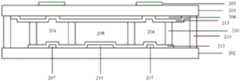
有鉴于此,本发明的实施例提供了一种功率分配网络。图2示意性地图示了包括根据本发明的一个实施例的功率分配网络的液晶天线200的顶视图,图3示意性地图示了沿图2中的A-A'方向的液晶天线200的截面视图,并且图4示意性地图示了沿图2中的B-B'方向的液晶天线200的截面视图。如图2-图4所示,液晶天线200包括相对设置的第一基板201和第二基板202。多个辐射元件203设置在第一基板201远离第二基板202的一侧上。液晶天线200包括功率分配网络,该功率分配网络配置成向该多个辐射元件203馈送电磁信号。功率分配网络包括多个级联的功率分配器205。每一个功率分配器205包括传输介质区208、设置在第二基板202与传输介质区208之间的第一微带线211,以及设置在第一基板201与传输介质区208之间的参考电极206。如图2所示,该多个功率分配器205的传输介质区208彼此连续。进一步地,液晶天线200包括移相器。该移相器包括设置在第一基板201与第二基板202之间的多个液晶区204、设置在第一基板201与该多个液晶区204之间的参考电极206,以及设置在第二基板202与该多个液晶区204之间的第二微带线207。第二微带线207配置成与参考电极206配合以控制每一个液晶区204中的液晶分子取向。In view of this, embodiments of the present invention provide a power distribution network. 2 schematically illustrates a top view of a liquid crystal antenna 200 including a power distribution network according to one embodiment of the present invention, and FIG. 3 schematically illustrates a cross-section of the liquid crystal antenna 200 along the AA' direction in FIG. 2 view, and FIG. 4 schematically illustrates a cross-sectional view of the liquid crystal antenna 200 along the BB' direction in FIG. 2 . As shown in FIG. 2-FIG. 4, the liquid crystal antenna 200 includes a
特别地,该多个液晶区204与该多个辐射元件203一一对应,每一个辐射元件203与对应的液晶区204在第二基板202上的正投影至少部分重叠,并且传输介质区208设置在相邻的液晶区204之间,如图3和图4所示。而且,每一个功率分配器205的传输介质区208中的传输介质的介质损耗角的正切值小于液晶区204中的液晶的介质损耗角的正切值。In particular, the plurality of
应当指出的是,尽管图2示意性地图示了一个2*2的液晶阵列天线,但是本发明的概念不限于此,而是可以适用于包括任何数目的阵元的液晶天线。进一步地,本发明的概念不仅适用于液晶微带天线,也适用于收发一体的液晶相控阵天线。It should be noted that although FIG. 2 schematically illustrates a 2*2 liquid crystal array antenna, the concept of the present invention is not limited thereto, but can be applied to liquid crystal antennas including any number of array elements. Further, the concept of the present invention is applicable not only to liquid crystal microstrip antennas, but also to liquid crystal phased array antennas with integrated transceivers.
在本发明的上述实施例中,在需要实现移相器功能的区域内提供液晶区,以保证移相器的大角度移相功能,而在其它区域,功率分配网络采用不同于液晶的另一传输介质,该传输介质的介质损耗角小于液晶的介质损耗角。如本文所使用的,术语“介质损耗角”又称为介电相位角,其为交流电压下电介质中的有功率分配量和无功率分配量的比值,并且反映电介质内单位体积中能量损耗的大小。相比于如图1所示的液晶天线100,通过将除需要实现移相器功能的区域之外的区域中的传输介质更换为介质损耗角更小(即单位体积中能量损耗更小)的传输介质,该液晶天线200的功率分配网络可以在保证将输入信号等幅同相地平均分配到各个阵元的前提下,大幅降低功率分配网络中由液晶产生的传输损耗。In the above-mentioned embodiments of the present invention, the liquid crystal area is provided in the area that needs to realize the function of the phase shifter to ensure the large-angle phase shifting function of the phase shifter, while in other areas, the power distribution network adopts another A transmission medium whose dielectric loss angle is smaller than that of the liquid crystal. As used herein, the term "dielectric loss angle" is also referred to as the dielectric phase angle, which is the ratio of the amount of power distribution to the amount of power distribution in the dielectric under AC voltage, and reflects the energy loss per unit volume in the dielectric size. Compared with the
在示例性实施例中,如图2和图4所示,第一微带线211包括多个不同阻抗的微带线211和211',并且每一个功率分配器205还包括电耦接在不同阻抗的第一微带线211和211'之间的第一阻抗变换器209。当负载阻抗和微带线特征阻抗不等或两段特征阻抗不同的微带线相连接时,所传输的信号会产生反射,进而产生传输损耗,因此可以在需要匹配阻抗的负载与微带线或两段微带线之间使用阻抗变换器来达到阻抗匹配,从而减少传输损耗。因此,如本文所使用的,术语“阻抗变换器”又可以称为阻抗匹配器。在如图2所示的2*2液晶阵列天线中,通过一分二的功率分配器级联方式将输入信号等幅同相地传输至各个阵元。在每一个分支点上,设置一个第一阻抗变换器209,以实现功率分配网络的阻抗匹配。In an exemplary embodiment, as shown in FIG. 2 and FIG. 4 , the
在一些示例实施例中,传输介质区208中的传输介质为空气。换言之,传输介质区208填充有空气。以此方式,可以简化液晶天线的制作工艺,降低液晶天线的制作成本。In some example embodiments, the transport medium in
可选地,如图2所示,传输介质区208与相邻的液晶区204可以通过挡墙210分离。在示例性实施例中,挡墙210可以由封框胶制成。例如,在制作过程中,通过封框胶对阵列天线内部的不同传输介质区进行隔离区分,在需要实现移相器功能的区域中滴注液晶,从而保证移相器的大角度移相功能。Optionally, as shown in FIG. 2 , the
特别地,在示例性实施例中,第一微带线的宽度可以满足下式:In particular, in an exemplary embodiment, the width of the first microstrip line may satisfy the following formula:

其中,

类似地,在示例性实施例中,第二微带线207的宽度可以满足下式:Similarly, in an exemplary embodiment, the width of the

其中,


在示例性实施例中,如图3和4所示,液晶天线200还可以可选地包括位于液晶区204与第二基板202之间的第一取向层212,以及位于液晶区204与第一基板201之间的第二取向层213。第一取向层212和第二取向层213相互配合以设定液晶区204的初始取向。In an exemplary embodiment, as shown in FIGS. 3 and 4 , the liquid crystal antenna 200 may optionally further include a
图5和图6分别示出微带线采用液晶和空气作为传输介质时的传输损耗的仿真结果。由于功率分配网络主要由微带线组成,不同功率分配网络的区别主要在于微带线的长度不同,而微带线的传输损耗又与其长度呈线性关系,因此,通过固定长度的微带线的损耗可推测包括其它不同长度的微带线的功率分配网络的损耗。对比图5和图6可知,在相同的功率分配网络结构下,微带线在这两种不同传输介质的传输损耗差异较明显。例如,如图5和图6所示,在12.5GHz频率处,空气传输介质相比于液晶传输介质,传输损耗降低了2.2111dB,因而将部分液晶变换成空气将大大提升微带线的传输效率。Figures 5 and 6 show the simulation results of the transmission loss when the microstrip line uses liquid crystal and air as the transmission medium, respectively. Since the power distribution network is mainly composed of microstrip lines, the difference between different power distribution networks is mainly that the length of the microstrip line is different, and the transmission loss of the microstrip line is linearly related to its length. The losses can be presumed to include losses in the power distribution network of other microstrip lines of different lengths. Comparing Fig. 5 and Fig. 6, it can be seen that under the same power distribution network structure, the transmission loss of the microstrip line in these two different transmission media is significantly different. For example, as shown in Figure 5 and Figure 6, at the frequency of 12.5GHz, the transmission loss of the air transmission medium is reduced by 2.2111dB compared with the liquid crystal transmission medium, so converting part of the liquid crystal into air will greatly improve the transmission efficiency of the microstrip line .
转向图4,由于传输介质的改变,因此在不同的传输介质、相同的厚度和特征阻抗的前提下,第一微带线211和第二微带线207的宽度不同。为了降低传输损耗,可以在第一微带线211与第二微带线207的连接处添加第二阻抗变换器215。第二阻抗变换器215在挡墙210处起始,并且其长度和线宽由挡墙210(特别地,封框胶)的介电常数决定。也就是说,不同类型的挡墙210对应不同长度和宽度的第二阻抗变换器215。Turning to FIG. 4 , due to the change of the transmission medium, under the premise of different transmission medium, the same thickness and characteristic impedance, the widths of the
进一步地,本发明的实施例还提供了一种通信设备,该通信设备采用上述任一种液晶天线。Further, an embodiment of the present invention also provides a communication device, and the communication device adopts any one of the above-mentioned liquid crystal antennas.
在这样的通信设备中,在需要实现移相器功能的区域内提供液晶区,以保证移相器的大角度移相功能,而在其它区域,功率分配网络采用不同于液晶的另一传输介质,该传输介质的介质损耗角小于液晶的介质损耗角。通过将除需要实现移相器功能的区域之外的区域中的传输介质更换为介质损耗角更小(即单位体积中能量损耗更小)的传输介质,通信设备中的液晶天线的功率分配网络可以在保证将输入信号等幅同相地平均分配到各个阵元的前提下,大幅降低功率分配网络中由液晶产生的传输损耗。In such a communication device, a liquid crystal region is provided in the region where the phase shifter function needs to be implemented to ensure the large-angle phase shift function of the phase shifter, while in other regions, the power distribution network uses another transmission medium different from liquid crystal , the dielectric loss angle of the transmission medium is smaller than that of the liquid crystal. By replacing the transmission medium in the area other than the area where the phase shifter function is required to be implemented with a transmission medium with a smaller dielectric loss angle (that is, smaller energy loss per unit volume), the power distribution network of liquid crystal antennas in communication equipment Under the premise of ensuring that the input signal is equally distributed to each array element with equal amplitude and phase, the transmission loss caused by the liquid crystal in the power distribution network can be greatly reduced.
除非另外定义,否则本公开使用的技术术语或者科学术语应当为本发明所属领域普通技术人员所理解的通常意义。本公开中使用的“第一”、“第二”以及类似的词语并不表示任何顺序、数量或者重要性,而只是用来区分不同的组成部分。同样,“一个”、“一”或者“该”等类似词语也不表示数量限制,而是表示存在至少一个。“包括”或者“包含”等类似的词语意指出现该词前面的元件或者物件涵盖出现在该词后面列举的元件或者物件及其等同,而不排除其他元件或者物件。“连接”或者“耦接”等类似的词语并非限定于物理的或者机械的连接,而是可以包括电性的连接,不管是直接的还是间接的。“上”、“下”、“左”、“右”等仅用于表示相对位置关系,当被描述对象的绝对位置改变后,则该相对位置关系也可能相应地改变。需要注意的是,在不冲突的前提下,上述实施例中的特征可以任意组合使用。Unless otherwise defined, technical or scientific terms used in the present disclosure should have the ordinary meaning as understood by one of ordinary skill in the art to which this invention belongs. As used in this disclosure, "first," "second," and similar terms do not denote any order, quantity, or importance, but are merely used to distinguish the various components. Likewise, words such as "a," "an," or "the" do not denote a limitation of quantity, but rather denote the presence of at least one. "Comprises" or "comprising" and similar words mean that the elements or things appearing before the word encompass the elements or things recited after the word and their equivalents, but do not exclude other elements or things. Words like "connected" or "coupled" are not limited to physical or mechanical connections, but may include electrical connections, whether direct or indirect. "Up", "Down", "Left", "Right", etc. are only used to represent the relative positional relationship, and when the absolute position of the described object changes, the relative positional relationship may also change accordingly. It should be noted that, on the premise of no conflict, the features in the above embodiments can be used in any combination.
以上所述,仅为本发明的具体实施方式,但本发明的保护范围并不局限于此,任何本领域普通技术人员在本发明揭露的技术范围内,可轻易想到的变化或替换,都应涵盖在本发明的保护范围之内。因此,本发明的保护范围应该以权利要求的保护范围为准。The above are only specific embodiments of the present invention, but the protection scope of the present invention is not limited to this. Any changes or substitutions that can be easily thought of by those of ordinary skill in the art within the technical scope disclosed by the present invention should be Included within the scope of protection of the present invention. Therefore, the protection scope of the present invention should be subject to the protection scope of the claims.
Claims (10)
Translated fromChinese


Priority Applications (3)
| Application Number | Priority Date | Filing Date | Title |
|---|---|---|---|
| CN201810676301.4ACN110649356A (en) | 2018-06-27 | 2018-06-27 | Power distribution network, LCD antenna and communication equipment |
| PCT/CN2019/093193WO2020001519A1 (en) | 2018-06-27 | 2019-06-27 | Power distribution network, liquid crystal antenna and communication device |
| US16/640,619US11450972B2 (en) | 2018-06-27 | 2019-06-27 | Power distribution network, liquid crystal antenna and communication device |
Applications Claiming Priority (1)
| Application Number | Priority Date | Filing Date | Title |
|---|---|---|---|
| CN201810676301.4ACN110649356A (en) | 2018-06-27 | 2018-06-27 | Power distribution network, LCD antenna and communication equipment |
Publications (1)
| Publication Number | Publication Date |
|---|---|
| CN110649356Atrue CN110649356A (en) | 2020-01-03 |
Family
ID=68985517
Family Applications (1)
| Application Number | Title | Priority Date | Filing Date |
|---|---|---|---|
| CN201810676301.4APendingCN110649356A (en) | 2018-06-27 | 2018-06-27 | Power distribution network, LCD antenna and communication equipment |
Country Status (3)
| Country | Link |
|---|---|
| US (1) | US11450972B2 (en) |
| CN (1) | CN110649356A (en) |
| WO (1) | WO2020001519A1 (en) |
Cited By (9)
| Publication number | Priority date | Publication date | Assignee | Title |
|---|---|---|---|---|
| CN111416191A (en)* | 2020-03-31 | 2020-07-14 | 苏治国 | Preparation method of broadband phase-adjustable phase shifter based on variable dielectric constant substrate |
| CN112186340A (en)* | 2020-09-29 | 2021-01-05 | 京东方科技集团股份有限公司 | Antenna and manufacturing method thereof |
| US11069976B1 (en) | 2020-04-15 | 2021-07-20 | Shanghai Tianma Micro-electronics Co., Ltd. | Phased-array antenna and control method of the same |
| CN113540767A (en)* | 2020-04-15 | 2021-10-22 | 上海天马微电子有限公司 | Phased array antenna and control method thereof |
| CN113594669A (en)* | 2021-07-30 | 2021-11-02 | 上海天马微电子有限公司 | Antenna and preparation method thereof |
| CN113871817A (en)* | 2020-06-30 | 2021-12-31 | 上海天马微电子有限公司 | Phase shifter, manufacturing method and antenna |
| CN114253015A (en)* | 2020-09-22 | 2022-03-29 | 成都天马微电子有限公司 | Liquid crystal antenna, manufacturing method thereof and communication equipment |
| US11670852B2 (en) | 2021-10-28 | 2023-06-06 | Shanghai Tianma Micro-electronics Co., Ltd. | Scanning antenna |
| WO2023206059A1 (en)* | 2022-04-26 | 2023-11-02 | 京东方科技集团股份有限公司 | Phase shifter and manufacturing method therefor, and electronic device |
Families Citing this family (7)
| Publication number | Priority date | Publication date | Assignee | Title |
|---|---|---|---|---|
| CN115699456A (en)* | 2020-06-10 | 2023-02-03 | 默克专利股份有限公司 | Steerable antenna and method of heating and/or annealing a steerable antenna |
| CN111817001B (en)* | 2020-07-14 | 2022-05-10 | 电子科技大学 | Ka wave band is based on 1X 4 plane phased array that liquid crystal reflective phase shifter |
| CN114002874A (en)* | 2020-07-28 | 2022-02-01 | 京东方科技集团股份有限公司 | Display panel and display device |
| CN114079159B (en) | 2020-08-13 | 2022-11-11 | 上海天马微电子有限公司 | Liquid crystal antenna |
| WO2022110013A1 (en)* | 2020-11-27 | 2022-06-02 | 京东方科技集团股份有限公司 | Phase shifter and antenna |
| US11990680B2 (en)* | 2021-03-18 | 2024-05-21 | Seoul National University R&Db Foundation | Array antenna system capable of beam steering and impedance control using active radiation layer |
| CN114006163B (en)* | 2021-11-22 | 2024-08-13 | 上海天马微电子有限公司 | Liquid crystal antenna and manufacturing method thereof |
Citations (9)
| Publication number | Priority date | Publication date | Assignee | Title |
|---|---|---|---|---|
| US20050110641A1 (en)* | 2002-03-18 | 2005-05-26 | Greg Mendolia | RFID tag reading system and method |
| CN103560324A (en)* | 2006-05-24 | 2014-02-05 | D·D·哈兹扎 | Antennas and Arrays Based on Variable Permittivity |
| CN103975483A (en)* | 2011-09-27 | 2014-08-06 | 默克专利股份有限公司 | Electronically steerable planar phased array antenna |
| CN203967224U (en)* | 2014-04-22 | 2014-11-26 | 成都玖信科技有限公司 | A kind of power divider of broadband and low consumption mounting structure |
| WO2018021093A1 (en)* | 2016-07-26 | 2018-02-01 | シャープ株式会社 | Scanning antenna and scanning antenna production method |
| CN107887694A (en)* | 2017-09-25 | 2018-04-06 | 北京航空航天大学 | A kind of frequency/polarization/direction figure independence restructural paster antenna for strengthening polarization reconfigurable ability using liquid crystal material |
| CN107978841A (en)* | 2018-01-16 | 2018-05-01 | 京东方科技集团股份有限公司 | Liquid crystal antenna substrate and preparation method thereof, liquid crystal aerial panel and preparation method thereof |
| CN108196405A (en)* | 2018-01-15 | 2018-06-22 | 京东方科技集团股份有限公司 | Liquid crystal phase shifter and electronic device |
| CN208298996U (en)* | 2018-06-27 | 2018-12-28 | 京东方科技集团股份有限公司 | Power distributing network, liquid crystal antenna and communication equipment |
Family Cites Families (5)
| Publication number | Priority date | Publication date | Assignee | Title |
|---|---|---|---|---|
| US9780451B2 (en) | 2013-11-05 | 2017-10-03 | Kymeta Corporation | Tunable resonator device and method of making same |
| US10686257B2 (en)* | 2016-09-01 | 2020-06-16 | Wafer Llc | Method of manufacturing software controlled antenna |
| US10608321B2 (en)* | 2017-05-23 | 2020-03-31 | Apple Inc. | Antennas in patterned conductive layers |
| CN107706502A (en)* | 2017-09-29 | 2018-02-16 | 京东方科技集团股份有限公司 | Antenna element and its manufacture method, liquid crystal antenna, communication equipment |
| WO2020066604A1 (en)* | 2018-09-27 | 2020-04-02 | 株式会社村田製作所 | Antenna module, communication device and array antenna |
- 2018
- 2018-06-27CNCN201810676301.4Apatent/CN110649356A/enactivePending
- 2019
- 2019-06-27WOPCT/CN2019/093193patent/WO2020001519A1/ennot_activeCeased
- 2019-06-27USUS16/640,619patent/US11450972B2/enactiveActive
Patent Citations (9)
| Publication number | Priority date | Publication date | Assignee | Title |
|---|---|---|---|---|
| US20050110641A1 (en)* | 2002-03-18 | 2005-05-26 | Greg Mendolia | RFID tag reading system and method |
| CN103560324A (en)* | 2006-05-24 | 2014-02-05 | D·D·哈兹扎 | Antennas and Arrays Based on Variable Permittivity |
| CN103975483A (en)* | 2011-09-27 | 2014-08-06 | 默克专利股份有限公司 | Electronically steerable planar phased array antenna |
| CN203967224U (en)* | 2014-04-22 | 2014-11-26 | 成都玖信科技有限公司 | A kind of power divider of broadband and low consumption mounting structure |
| WO2018021093A1 (en)* | 2016-07-26 | 2018-02-01 | シャープ株式会社 | Scanning antenna and scanning antenna production method |
| CN107887694A (en)* | 2017-09-25 | 2018-04-06 | 北京航空航天大学 | A kind of frequency/polarization/direction figure independence restructural paster antenna for strengthening polarization reconfigurable ability using liquid crystal material |
| CN108196405A (en)* | 2018-01-15 | 2018-06-22 | 京东方科技集团股份有限公司 | Liquid crystal phase shifter and electronic device |
| CN107978841A (en)* | 2018-01-16 | 2018-05-01 | 京东方科技集团股份有限公司 | Liquid crystal antenna substrate and preparation method thereof, liquid crystal aerial panel and preparation method thereof |
| CN208298996U (en)* | 2018-06-27 | 2018-12-28 | 京东方科技集团股份有限公司 | Power distributing network, liquid crystal antenna and communication equipment |
Non-Patent Citations (2)
| Title |
|---|
| E.HAMMERSTAD等: "Accurate Models for Microstrip Computer Aided Design", 1980 IEEE MTT-S INTERNATIONAL MICROWAVE SYMPOSIUM DIGEST, 6 January 2003 (2003-01-06), pages 407 - 409* |
| E.HAMMERSTAD等: "Accurate_Models_for_Microstrip_Computer-Aided_Design", 1980 IEEE MTT-S INTERNATIONAL MICROWAVE SYMPOSIUM DIGEST, 6 January 2003 (2003-01-06), pages 407 - 409* |
Cited By (15)
| Publication number | Priority date | Publication date | Assignee | Title |
|---|---|---|---|---|
| CN111416191A (en)* | 2020-03-31 | 2020-07-14 | 苏治国 | Preparation method of broadband phase-adjustable phase shifter based on variable dielectric constant substrate |
| CN111416191B (en)* | 2020-03-31 | 2021-08-13 | 苏治国 | Preparation method of broadband phase-adjustable phase shifter based on variable dielectric constant substrate |
| US11196172B2 (en) | 2020-04-15 | 2021-12-07 | Shanghai Tianma Micro-electronics Co., Ltd. | Phased-array antenna and method for controlling the same |
| US11069976B1 (en) | 2020-04-15 | 2021-07-20 | Shanghai Tianma Micro-electronics Co., Ltd. | Phased-array antenna and control method of the same |
| CN113540767A (en)* | 2020-04-15 | 2021-10-22 | 上海天马微电子有限公司 | Phased array antenna and control method thereof |
| CN113540766A (en)* | 2020-04-15 | 2021-10-22 | 上海天马微电子有限公司 | Phased array antenna and control method thereof |
| CN113871817A (en)* | 2020-06-30 | 2021-12-31 | 上海天马微电子有限公司 | Phase shifter, manufacturing method and antenna |
| CN114253015A (en)* | 2020-09-22 | 2022-03-29 | 成都天马微电子有限公司 | Liquid crystal antenna, manufacturing method thereof and communication equipment |
| US11469500B2 (en) | 2020-09-22 | 2022-10-11 | Chengdu Tianma Micro-Electronics Co., Ltd. | Liquid crystal antenna, manufacturing method thereof and communication device |
| CN114253015B (en)* | 2020-09-22 | 2024-04-19 | 成都天马微电子有限公司 | Liquid crystal antenna, manufacturing method thereof and communication equipment |
| CN112186340A (en)* | 2020-09-29 | 2021-01-05 | 京东方科技集团股份有限公司 | Antenna and manufacturing method thereof |
| CN112186340B (en)* | 2020-09-29 | 2023-11-07 | 京东方科技集团股份有限公司 | Antenna and manufacturing method thereof |
| CN113594669A (en)* | 2021-07-30 | 2021-11-02 | 上海天马微电子有限公司 | Antenna and preparation method thereof |
| US11670852B2 (en) | 2021-10-28 | 2023-06-06 | Shanghai Tianma Micro-electronics Co., Ltd. | Scanning antenna |
| WO2023206059A1 (en)* | 2022-04-26 | 2023-11-02 | 京东方科技集团股份有限公司 | Phase shifter and manufacturing method therefor, and electronic device |
Also Published As
| Publication number | Publication date |
|---|---|
| WO2020001519A1 (en) | 2020-01-02 |
| US11450972B2 (en) | 2022-09-20 |
| US20200185836A1 (en) | 2020-06-11 |
Similar Documents
| Publication | Publication Date | Title |
|---|---|---|
| CN110649356A (en) | Power distribution network, LCD antenna and communication equipment | |
| CN208298996U (en) | Power distributing network, liquid crystal antenna and communication equipment | |
| CN112768851B (en) | Feed structure, microwave radio frequency device and antenna | |
| CN113555677B (en) | Feed system, antenna system and base station | |
| CN109921190B (en) | Signal conditioner, antenna device, and method of manufacture | |
| CN104953256A (en) | Broadband circularly-polarized panel array antenna | |
| CN207611862U (en) | An array antenna for realizing multi-mode vortex electromagnetic waves | |
| KR101663139B1 (en) | High-efficient rf transmission line structure and its application components | |
| CN108110425A (en) | 2 × 4 wideband butler matrix plates, butler matrix and multibeam antenna | |
| CN114927869B (en) | Millimeter wave dual-beam dielectric resonator antenna | |
| WO2018121256A9 (en) | Low profile antenna | |
| WO2022111170A1 (en) | Antenna and manufacturing and driving methods therefor, and antenna system | |
| CN111048879B (en) | A broadband constant amplitude conversion structure from rectangular waveguide to double-terminal stripline | |
| CN114824779B (en) | A single-layer low-profile broadband dual-polarized patch antenna | |
| CN115775964B (en) | A new coupler with reconfigurable coupling coefficient based on HMCSIW | |
| CN208045696U (en) | A kind of Butler matrix feed networks based on substrate integration wave-guide | |
| CN117060076A (en) | Broadband dual-polarized ultra-surface indoor access point antenna | |
| US20230155285A1 (en) | Antenna | |
| US20230071974A1 (en) | Antenna and manufacturing method thereof | |
| US20230163478A1 (en) | Antenna and manufacturing method thereof | |
| CN205178018U (en) | Integrated waveguide horn antenna of two circular polarization substrates in plane | |
| WO2022247624A1 (en) | Microstrip antenna structure and communication device | |
| CN110797652B (en) | Periodic leaky-wave antenna with CPW structure and preparation method | |
| CN105680143B (en) | Waveguide T-type mixing knot based on ferroelectric material and design method | |
| CN221726351U (en) | An integrated liquid crystal phased array |
Legal Events
| Date | Code | Title | Description |
|---|---|---|---|
| PB01 | Publication | ||
| PB01 | Publication | ||
| SE01 | Entry into force of request for substantive examination | ||
| SE01 | Entry into force of request for substantive examination |