CN110646493A - A microfluidic chip, protein detection method, device and system - Google Patents
A microfluidic chip, protein detection method, device and systemDownload PDFInfo
- Publication number
- CN110646493A CN110646493ACN201910913923.9ACN201910913923ACN110646493ACN 110646493 ACN110646493 ACN 110646493ACN 201910913923 ACN201910913923 ACN 201910913923ACN 110646493 ACN110646493 ACN 110646493A
- Authority
- CN
- China
- Prior art keywords
- electrode
- solid
- chip
- tested
- microfluidic chip
- Prior art date
- Legal status (The legal status is an assumption and is not a legal conclusion. Google has not performed a legal analysis and makes no representation as to the accuracy of the status listed.)
- Pending
Links
Images


Classifications
- G—PHYSICS
- G01—MEASURING; TESTING
- G01N—INVESTIGATING OR ANALYSING MATERIALS BY DETERMINING THEIR CHEMICAL OR PHYSICAL PROPERTIES
- G01N27/00—Investigating or analysing materials by the use of electric, electrochemical, or magnetic means
- G01N27/26—Investigating or analysing materials by the use of electric, electrochemical, or magnetic means by investigating electrochemical variables; by using electrolysis or electrophoresis
- G01N27/416—Systems
- G—PHYSICS
- G01—MEASURING; TESTING
- G01N—INVESTIGATING OR ANALYSING MATERIALS BY DETERMINING THEIR CHEMICAL OR PHYSICAL PROPERTIES
- G01N21/00—Investigating or analysing materials by the use of optical means, i.e. using sub-millimetre waves, infrared, visible or ultraviolet light
- G01N21/75—Systems in which material is subjected to a chemical reaction, the progress or the result of the reaction being investigated
- G01N21/76—Chemiluminescence; Bioluminescence
Landscapes
- Chemical & Material Sciences (AREA)
- Physics & Mathematics (AREA)
- Life Sciences & Earth Sciences (AREA)
- Health & Medical Sciences (AREA)
- Biochemistry (AREA)
- Chemical Kinetics & Catalysis (AREA)
- Analytical Chemistry (AREA)
- General Health & Medical Sciences (AREA)
- General Physics & Mathematics (AREA)
- Immunology (AREA)
- Pathology (AREA)
- Electrochemistry (AREA)
- Molecular Biology (AREA)
- Engineering & Computer Science (AREA)
- Plasma & Fusion (AREA)
- Investigating Or Analysing Materials By The Use Of Chemical Reactions (AREA)
Abstract
Translated fromChineseDescription
Translated fromChinese技术领域technical field
本发明涉及蛋白检测领域,尤其涉及一种微流控芯片、一种双极性电极芯片、一种双极性电极的制作工艺、一种蛋白检测系统、一种蛋白检测装置以及一种蛋白检测方法。The invention relates to the field of protein detection, in particular to a microfluidic chip, a bipolar electrode chip, a manufacturing process of a bipolar electrode, a protein detection system, a protein detection device and a protein detection method.
背景技术Background technique
随着转化医学和精准医学的快速发展,对细胞、核酸、蛋白等基本生物单元的研究发生了深刻的变革,目前已从传统的对这些单元的系综和平均化响应的研究,转向到了单细胞和单分子水平的研究。特别是在分子诊断领域,需要在单分子层面精确诊断患者的健康水平以及治疗效果,以便早期诊断,大大提前诊疗窗口,达到治未病的效果。因此需要开发与之相适应的高灵敏度、早诊断的生物单元检测方法。With the rapid development of translational medicine and precision medicine, the research on basic biological units such as cells, nucleic acids, and proteins has undergone profound changes. At present, the traditional research on the ensemble and averaged responses of these units has shifted to a single Studies at the cellular and single-molecule levels. Especially in the field of molecular diagnosis, it is necessary to accurately diagnose the health level and treatment effect of patients at the single-molecule level, so as to facilitate early diagnosis, greatly advance the diagnosis and treatment window, and achieve the effect of treating the disease before it occurs. Therefore, it is necessary to develop a suitable high-sensitivity, early-diagnosis biological unit detection method.
在痕量蛋白检测领域,样品中待检测的蛋白的含量往往在百万分之一以下,且对细胞功能产生重大影响的蛋白质其表达量往往是很低的,由于缺少与聚合酶链式反应(PCR,Polymerase Chain Reaction)媲美的高信号放大方法,其在常规检测方法中很难被检测到。目前对于痕量蛋白检测的主要方法包括生物质谱技术和数字酶联免疫吸附测定(ELISA,enzyme linked immunosorbent assay)技术。生物质谱技术主要应用于科研领域,由于成本高,操作复杂,很难实现临床的大批量应用。数字ELISA技术中,由于免疫反应过程不稳定,不方便进行有效控制,使得痕量蛋白检测的一致性和重复性较差。In the field of trace protein detection, the content of the protein to be detected in the sample is often less than one part per million, and the expression of the protein that has a major impact on cell function is often very low, due to the lack of interaction with polymerase chain reaction. (PCR, Polymerase Chain Reaction) comparable high signal amplification method, which is difficult to be detected in conventional detection methods. At present, the main methods for trace protein detection include biological mass spectrometry technology and digital enzyme linked immunosorbent assay (ELISA, enzyme linked immunosorbent assay) technology. Biomass spectrometry is mainly used in scientific research. Due to the high cost and complex operation, it is difficult to achieve large-scale clinical applications. In digital ELISA technology, due to the unstable immune reaction process, it is inconvenient to effectively control, which makes the consistency and repeatability of trace protein detection poor.
发明内容SUMMARY OF THE INVENTION
本发明实施例提供一种微流控芯片、一种双极性电极芯片、一种双极性电极的制作工艺、一种蛋白检测系统、一种蛋白检测装置以及一种蛋白检测方法,以解决现有技术中由于免疫反应过程不稳定,不方便进行有效控制,使得痕量蛋白检测的一致性和重复性较差的问题。Embodiments of the present invention provide a microfluidic chip, a bipolar electrode chip, a manufacturing process for a bipolar electrode, a protein detection system, a protein detection device, and a protein detection method, so as to solve the problem of In the prior art, due to the unstable immune reaction process, it is inconvenient to carry out effective control, resulting in the problem of poor consistency and repeatability of trace protein detection.
本发明实施例采用下述技术方案:The embodiment of the present invention adopts the following technical solutions:
第一方面,本发明实施例提供了一种蛋白检测系统,包括:In a first aspect, an embodiment of the present invention provides a protein detection system, including:
微流控芯片,包括呈阵列排布的多个微阱,所述微阱用于捕获被测样品中的固相载体;被测样品中包括:结合了被测蛋白及电化学发光材料的固相载体、未结合被测蛋白及电化学发光材料的固相载体、电化学反应溶液;The microfluidic chip includes a plurality of microwells arranged in an array, and the microwells are used to capture the solid-phase carrier in the tested sample; Phase carrier, solid phase carrier that is not bound to the tested protein and electrochemiluminescent material, and electrochemical reaction solution;
双极性电极芯片,包括呈阵列排布的多个电极单元,所述电极单元在所述被测样品中被激活时,与电化学发光材料发生电化学反应并发光;The bipolar electrode chip includes a plurality of electrode units arranged in an array, and when the electrode units are activated in the tested sample, electrochemical reaction occurs with the electrochemiluminescent material and emits light;
浓度确定组件,根据所述微阱中固相载体的总数量和发光固相载体的数量,确定被测样品中被测蛋白的浓度值。The concentration determination component determines the concentration value of the tested protein in the tested sample according to the total number of solid-phase carriers and the number of luminescent solid-phase carriers in the microwell.
结合第一方面,本发明实施例提供了第一方面的一种可能的实施方式,所述微流控芯片和所述双极性电极芯片可拆卸连接;In conjunction with the first aspect, the embodiment of the present invention provides a possible implementation manner of the first aspect, wherein the microfluidic chip and the bipolar electrode chip are detachably connected;
所述微流控芯片设置有第一对准结构,所述双极性电极芯片设置有第二对准结构,所述第一对准结构和所述第二对准结构配合以将所述微阱和所述电极单元一一对准。The microfluidic chip is provided with a first alignment structure, the bipolar electrode chip is provided with a second alignment structure, and the first alignment structure and the second alignment structure cooperate to align the microfluidic chip. The wells and the electrode units are aligned one by one.
结合第一方面,本发明实施例提供了第一方面的一种可能的实施方式,所述浓度确定组件,具体包括:In conjunction with the first aspect, the embodiment of the present invention provides a possible implementation manner of the first aspect. The concentration determination component specifically includes:
电位控制器,用于控制电极单元两端的电压,以激活所述电极单元;a potential controller for controlling the voltage across the electrode unit to activate the electrode unit;
光学成像模块,用于对所述微流控芯片中的所有固相载体进行扫描成像,以及对微流控芯片中发光的固相载体进行扫描成像;an optical imaging module, used for scanning and imaging all solid-phase carriers in the microfluidic chip, and scanning and imaging the solid-phase carriers that emit light in the microfluidic chip;
图像分析模块,用于对扫描成像得到的图像进行分析,得到固相载体总数量和发光的固相载体数量;The image analysis module is used to analyze the image obtained by scanning and imaging to obtain the total number of solid-phase carriers and the number of luminescent solid-phase carriers;
浓度确定模块,用于通过泊松分布概率公式,根据固相载体总数量和发光的固相载体的数量,确定被测样品中被测蛋白的浓度值。The concentration determination module is used to determine the concentration value of the tested protein in the tested sample according to the total number of solid-phase carriers and the quantity of luminescent solid-phase carriers through the Poisson distribution probability formula.
第二方面,本发明实施例提供了一种微流控芯片,包括:In a second aspect, an embodiment of the present invention provides a microfluidic chip, including:
固相载体平铺区域,所述固相载体平铺区域包括多条液体导流槽,以及位于液体导流槽底部的微阱,所述微阱在所述微流控芯片上呈阵列排布。a solid-phase carrier tiling area, the solid-phase carrier tiling area includes a plurality of liquid guiding grooves, and a micro-well located at the bottom of the liquid guiding groove, the micro-wells are arranged in an array on the microfluidic chip .
结合第二方面,本发明实施例提供了第二方面的一种可能的实施方式,所述微流控芯片包括位于所述固相载体平铺区域一端的加样区域,以及位于所述固相载体平铺区域另一端的溢流缓冲区域,所述加样区域和所述溢流缓冲区域通过所述导流槽连通。In conjunction with the second aspect, the embodiment of the present invention provides a possible implementation of the second aspect, wherein the microfluidic chip includes a sample application area located at one end of the solid-phase carrier tiling area, and a sample application area located on the solid-phase carrier tiling area. The overflow buffer area at the other end of the carrier tiling area, the sample adding area and the overflow buffer area communicate with each other through the guide groove.
结合第二方面,本发明实施例提供了第二方面的一种可能的实施方式,每个所述微阱为斜坡结构,斜坡高点为导流槽底部,位于靠近加样区的一侧,斜坡越靠近溢流缓冲区域的一侧越深,每个所述微阱仅能容纳一个固相载体。In conjunction with the second aspect, the embodiment of the present invention provides a possible implementation of the second aspect, each of the microwells is a slope structure, and the high point of the slope is the bottom of the guide groove, located on the side close to the sample adding area, The deeper the slope is on the side closer to the overflow buffer region, each of the microwells can only accommodate one solid phase carrier.
第三方面,本发明实施例提供了一种双极性电极芯片,包括:In a third aspect, an embodiment of the present invention provides a bipolar electrode chip, including:
呈阵列排布的多个电极单元,所述电极单元在所述被测样品中被激活时,与电化学发光材料发生电化学反应并发光;a plurality of electrode units arranged in an array, when the electrode units are activated in the tested sample, electrochemical reaction occurs with the electrochemiluminescent material and emits light;
所述电极单元的阳极端面积小于阴极端面积。The anode end area of the electrode unit is smaller than the cathode end area.
结合第三方面,本发明实施例提供了第三方面的一种可能的实施方式,所述电极单元平行于电极板的横截面为三角形,所述三角形的一边为阴极,与所述边相对的角的顶点为阳极;In conjunction with the third aspect, an embodiment of the present invention provides a possible implementation of the third aspect, wherein the cross section of the electrode unit parallel to the electrode plate is a triangle, one side of the triangle is the cathode, and the side opposite to the side is a triangle. The vertex of the angle is the anode;
或,所述电极单元平行于电极板的横截面为桃形,所述桃型的顶点为阳极,与所述桃型的顶点相对的边为阴极。Or, a cross section of the electrode unit parallel to the electrode plate is a peach shape, the apex of the peach shape is the anode, and the side opposite to the apex of the peach shape is the cathode.
结合第三方面,本发明实施例提供了第三方面的一种可能的实施方式,所述电极单元包括电极修饰层;In conjunction with the third aspect, the embodiment of the present invention provides a possible implementation manner of the third aspect, wherein the electrode unit includes an electrode modification layer;
所述电极修饰层的电极修饰材料为铂;或,所述电极修饰层的电极修饰材料为铂-氧化铱复合纳米材料。The electrode modification material of the electrode modification layer is platinum; or, the electrode modification material of the electrode modification layer is a platinum-iridium oxide composite nanomaterial.
结合第三方面,本发明实施例提供了第三方面的一种可能的实施方式,单个所述电极单元的粒径为5-30μm,所述双极性电极芯片中电极单元的总数量大于20000个。In conjunction with the third aspect, the embodiment of the present invention provides a possible implementation of the third aspect, the particle size of a single electrode unit is 5-30 μm, and the total number of electrode units in the bipolar electrode chip is greater than 20,000 indivual.
第四方面,本发明实施例提供了一种双极性电极的制作工艺,包括;In a fourth aspect, an embodiment of the present invention provides a process for fabricating a bipolar electrode, including:
在衬底基板上形成一层反转胶,通过光刻技术在反转胶上形成电极层图案;A layer of reverse glue is formed on the base substrate, and an electrode layer pattern is formed on the reverse glue by photolithography;
在形成有所述电极层图案的玻璃衬底上形成电极层,所述电极层的材料为钛/铂复合材料;forming an electrode layer on the glass substrate formed with the electrode layer pattern, and the material of the electrode layer is a titanium/platinum composite material;
将所述衬底基板上的反转胶剥离,得到电极阵列;peeling off the reverse glue on the base substrate to obtain an electrode array;
通过化学电镀的方式,在所述电极阵列表面形成一层电极修饰层,所述电极修饰层的材料为铂或铂-氧化铱复合纳米材料;By means of chemical electroplating, an electrode modification layer is formed on the surface of the electrode array, and the material of the electrode modification layer is platinum or platinum-iridium oxide composite nanomaterials;
在所述电极阵列表面形成一层光刻胶,以保护所述电极阵列,通过光刻技术在电极阵列的两侧形成第二对准结构,然后去除所述电极阵列表面上的光刻胶,露出电极部分。A layer of photoresist is formed on the surface of the electrode array to protect the electrode array, a second alignment structure is formed on both sides of the electrode array by photolithography, and then the photoresist on the surface of the electrode array is removed, The electrode portion is exposed.
第五方面,本发明实施例提供了一种蛋白检测装置,包括本发明实施例提供的蛋白检测系统,所述装置还包括抽屉模组和人机交互模组,其中:In a fifth aspect, the embodiment of the present invention provides a protein detection device, including the protein detection system provided by the embodiment of the present invention, and the device further includes a drawer module and a human-computer interaction module, wherein:
所述抽屉模组,用于承载微流控芯片,并将微流控芯片运动至蛋白检测系统的光学成像模块中进行成像;The drawer module is used to carry the microfluidic chip, and move the microfluidic chip to the optical imaging module of the protein detection system for imaging;
所述人机交互模块,用于输入检测参数和输出检测结果。The human-computer interaction module is used for inputting detection parameters and outputting detection results.
第六方面,本发明实施例提供了一种蛋白检测方法,包括如下步骤:In a sixth aspect, the embodiment of the present invention provides a protein detection method, comprising the following steps:
在微流控芯片的加样区域加入被测样品;所述被测样品中包括:结合了被测蛋白及电化学发光材料的固相载体、未结合被测蛋白及电化学发光材料的固相载体、电化学反应溶液;The sample to be tested is added to the sample application area of the microfluidic chip; the sample to be tested includes: a solid phase carrier bound with the tested protein and electrochemiluminescent material, and a solid phase unbound to the tested protein and electrochemiluminescent material Carrier, electrochemical reaction solution;
将双极性电极芯片盖到所述微流控芯片上,并将所述双极性电极芯片上的微阱和双极性电极芯片上的电极单元一一对准;Covering the bipolar electrode chip on the microfluidic chip, and aligning the microwells on the bipolar electrode chip and the electrode units on the bipolar electrode chip one by one;
在明场条件下,在所述双极性电极芯片两端不施加电压的前提下,对微流控芯片的固相载体平铺区域进行光学扫描成像,得到第一图像,并计算第一图像中固相载体的总数量;Under bright field conditions, on the premise that no voltage is applied to both ends of the bipolar electrode chip, optically scan and image the tiled area of the solid-phase carrier of the microfluidic chip to obtain a first image, and calculate the first image The total number of solid-phase carriers in the medium;
在暗场条件下,对所述双极性电极芯片两端施加电压,对微流控芯片的固相载体平铺区域进行光学扫描成像,得到第二图像,并计算第二图像中发光的固相载体的数量;Under dark field conditions, a voltage is applied to both ends of the bipolar electrode chip, and optical scanning imaging is performed on the tiled area of the solid-phase carrier of the microfluidic chip to obtain a second image, and the luminescent solid state in the second image is calculated. the number of phase carriers;
通过泊松分布概率公式,根据固相载体的总数量和发光的固相载体的数量,确定被测样品中被测蛋白的浓度值。Through the Poisson distribution probability formula, the concentration value of the tested protein in the tested sample is determined according to the total number of solid phase carriers and the number of luminescent solid phase carriers.
本发明实施例采用的上述至少一个技术方案能够达到以下有益效果:The above-mentioned at least one technical solution adopted in the embodiment of the present invention can achieve the following beneficial effects:
在被测样品中,通过在固相载体上结合电化学发光材料和被测蛋白,微流控芯片上的微阱可以捕获被测样品中的固相载体,双极性电极中的电极单元在被激活时与电学发光材料发生电化学反应并发光,以此即可确定结合有被测蛋白的固相载体的数量,根据结合有被测蛋白的固相载体的数量和微阱中固相载体的总数量,即可确定被测样品中被测蛋白的浓度值。由于电致化学发光是一种非常可控的反应体系,其电压作为反应的启动开关,能有效的消除由于试剂添加或者混合带来的反应不稳定的问题,从而保证反应过程在完全可控的条件下进行。该反应过程具有灵敏度高,线性范围宽,反应时间短,试剂稳定时间长等优势。将电致化学发光检测技术与单分子蛋白检测技术的完美结合,可以充分发挥两个技术的各自优势,实现高灵敏的单分子检测。In the sample to be tested, by combining the electrochemiluminescent material and the protein to be tested on the solid-phase carrier, the micro-well on the microfluidic chip can capture the solid-phase carrier in the sample to be tested, and the electrode unit in the bipolar electrode is in the When activated, it reacts electrochemically with the electroluminescent material and emits light, so that the number of solid-phase carriers bound to the tested protein can be determined. The total quantity of the tested protein can be determined to determine the concentration value of the tested protein in the tested sample. Since electrochemiluminescence is a very controllable reaction system, its voltage is used as the start switch of the reaction, which can effectively eliminate the problem of instability of the reaction caused by the addition or mixing of reagents, thereby ensuring that the reaction process is completely controllable. conditions. The reaction process has the advantages of high sensitivity, wide linear range, short reaction time, and long reagent stabilization time. The perfect combination of electrochemiluminescence detection technology and single-molecule protein detection technology can give full play to the respective advantages of the two technologies to achieve highly sensitive single-molecule detection.
附图说明Description of drawings
此处所说明的附图用来提供对本发明的进一步理解,构成本发明的一部分,本发明的示意性实施例及其说明用于解释本发明,并不构成对本发明的不当限定。在附图中:The accompanying drawings described herein are used to provide further understanding of the present invention and constitute a part of the present invention. The exemplary embodiments of the present invention and their descriptions are used to explain the present invention and do not constitute an improper limitation of the present invention. In the attached image:
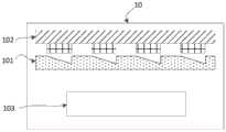
图1为本发明实施例提供的一种蛋白检测系统的结构示意图;1 is a schematic structural diagram of a protein detection system provided in an embodiment of the present invention;
图2为本发明实施例提供的双极性电极的工作原理示意图;2 is a schematic diagram of the working principle of a bipolar electrode provided by an embodiment of the present invention;
图3为本发明实施例提供的一种微流控芯片的结构示意图;3 is a schematic structural diagram of a microfluidic chip according to an embodiment of the present invention;
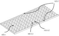
图4为本发明实施例提供的一种双极性电极芯片的结构示意图;4 is a schematic structural diagram of a bipolar electrode chip according to an embodiment of the present invention;
图5为本发明实施例提供的另一种双极性电极芯片的结构示意图;5 is a schematic structural diagram of another bipolar electrode chip provided by an embodiment of the present invention;
图6为本发明实施例提供的一种双极性电极制作工艺的流程示意图;FIG. 6 is a schematic flowchart of a bipolar electrode fabrication process according to an embodiment of the present invention;
图7为本发明实施例提供的一种蛋白检测装置的结构示意图;7 is a schematic structural diagram of a protein detection device according to an embodiment of the present invention;
图8为本发明实施例提供的一种蛋白检测系统的结构示意图;8 is a schematic structural diagram of a protein detection system according to an embodiment of the present invention;
图9为本发明实施例提供的一种蛋白检测方法实现流程示意图。FIG. 9 is a schematic diagram of the implementation flow of a protein detection method provided in an embodiment of the present invention.
具体实施方式Detailed ways
为使本发明的目的、技术方案和优点更加清楚,下面将结合本发明具体实施例及相应的附图对本发明技术方案进行清楚、完整地描述。显然,所描述的实施例仅是本发明一部分实施例,而不是全部的实施例。基于本发明中的实施例,本领域普通技术人员在没有做出创造性劳动前提下所获得的所有其他实施例,都属于本发明保护的范围。In order to make the objectives, technical solutions and advantages of the present invention clearer, the technical solutions of the present invention will be clearly and completely described below with reference to the specific embodiments of the present invention and the corresponding drawings. Obviously, the described embodiments are only some, but not all, embodiments of the present invention. Based on the embodiments of the present invention, all other embodiments obtained by those of ordinary skill in the art without creative efforts shall fall within the protection scope of the present invention.
以下结合附图,详细说明本发明各实施例提供的技术方案。The technical solutions provided by the embodiments of the present invention will be described in detail below with reference to the accompanying drawings.
实施例1Example 1
为解决现有技术中由于免疫反应过程不稳定,不方便进行有效控制,使得痕量蛋白检测的一致性和重复性较差的问题,本发明实施例1提供一种蛋白检测系统10,请参见图1,该蛋白检测系统10包括微流控芯片101、双极性电极芯片102和浓度确定组件103,其中:In order to solve the problem in the prior art that due to the instability of the immune reaction process, it is inconvenient to carry out effective control, and the consistency and repeatability of trace protein detection are poor. Embodiment 1 of the present invention provides a
微流控芯片101,包括呈阵列排布的多个微阱,所述微阱用于捕获被测样品中的固相载体;被测样品中包括:结合了被测蛋白及电化学发光材料的固相载体、未结合被测蛋白及电化学发光材料的固相载体、电化学反应溶液;The
双极性电极芯片102,包括呈阵列排布的多个电极单元,所述电极单元在所述被测样品中被激活时,与电化学发光材料发生电化学反应并发光;The
浓度确定组件103,根据所述微阱中固相载体的总数量和发光固相载体的数量,确定被测样品中被测蛋白的浓度值。The
本说明书实施例中,在被测样品中,会加入固相载体,固相载体具备较好的蛋白吸附能力,可以与被测蛋白相结合,优选的,固相载体可以是以聚苯乙烯制成磁珠,磁珠也可以称为磁微粒等。当然固相载体也可以是由其它能结合被测蛋白的材料制成,例如,氯乙酰化,本发明对此不作限定。In the examples of this specification, a solid-phase carrier is added to the sample to be tested. The solid-phase carrier has good protein adsorption capacity and can be combined with the tested protein. Preferably, the solid-phase carrier can be made of polystyrene. Magnetic beads can also be called magnetic particles, etc. Of course, the solid phase carrier can also be made of other materials that can bind the protein to be tested, for example, chloroacetylation, which is not limited in the present invention.
另外,结合了被测蛋白的固相载体也结合了电化学发光材料,优选的,电化学发光材料可以是三联吡啶钌(Ru(bpy)32+)。被测样品中还包括有电化学反应溶液,优选的,电化学反应溶液可以是三丙胺(TPrA)。加入微流控芯片的样本中抗原抗体已经完成免疫结合反应,并且磁分离了未结合的游离态蛋白。In addition, the solid-phase carrier that binds the protein to be tested also binds an electrochemiluminescent material. Preferably, the electrochemiluminescent material may be ruthenium terpyridine (Ru(bpy)32+). The tested sample also includes an electrochemical reaction solution, preferably, the electrochemical reaction solution may be tripropylamine (TPrA). The antigen-antibody in the sample added to the microfluidic chip has completed the immune binding reaction, and the unbound free protein has been magnetically separated.
将被测样品加入微流控芯片上后,微流控芯片上的微阱可以捕获被测样品中的固相载体,双极性电极中的电极单元在被激活时与电学发光材料发生电化学反应并发光,以此即可确定结合有被测蛋白的固相载体的数量,根据结合有被测蛋白的固相载体的数量和微阱中固相载体的总数量,即可确定被测样品中被测蛋白的浓度值。After the sample to be tested is added to the microfluidic chip, the micro-well on the microfluidic chip can capture the solid-phase carrier in the sample to be tested, and the electrode unit in the bipolar electrode undergoes electrochemistry with the electroluminescent material when activated. After reacting and emitting light, the number of solid-phase carriers bound to the protein to be tested can be determined. According to the number of solid-phase carriers bound to the tested protein and the total number of solid-phase carriers in the microwell, the sample to be tested can be determined. the concentration of the tested protein.
图2为双极性电极的工作原理示意图,双极性电极装置主要是由连接到直流电源上的驱动导体202和浸在电化学反应溶液203中的高密度电极阵列组成。电极阵列包含多个电极单元102-1,电极阵列可以是铁丝、铜片、金属纳米颗粒等任何形状和任何尺寸的导电材料。当直流电源201施加足够高的驱动电压(Etot)驱动导体时,尽管驱动导体和高密度电极阵列没有直接接触,在电极两端的附近溶液也能发生电化学反应。双极性电极阵列靠近导体负极的一端带正电,成为双极性电极的阳极102-1-2,双极性电极阵列靠近导体正极的一端带负电,成为双极性电极的阴极102-1-1。在双极性电极阵列的阳极表面,三联吡啶钌(Ru(bpy)32+)和三丙胺(TPrA)同时失去电子发生氧化反应,从而触发循环的电化学发光反应,电极单元102-1两端形成电势差ΔEelec。2 is a schematic diagram of the working principle of the bipolar electrode. The bipolar electrode device is mainly composed of a driving
本说明书提供的蛋白检测系统,尤其适用于对痕量蛋白进行检测,由于电致化学发光是一种非常可控的反应体系,其电压作为反应的启动开关,能有效的消除由于试剂添加或者混合带来的反应不稳定的问题,从而保证反应过程在完全可控的条件下进行。该反应过程具有灵敏度高,线性范围宽,反应时间短,试剂稳定时间长等优势。将电致化学发光检测技术与单分子蛋白检测技术的完美结合,可以充分发挥两个技术的各自优势,实现高灵敏的单分子检测。The protein detection system provided in this manual is especially suitable for the detection of trace proteins. Since electrochemiluminescence is a very controllable reaction system, its voltage is used as the start switch of the reaction, which can effectively eliminate the need for reagent addition or mixing. The problem of instability of the reaction is brought about, so as to ensure that the reaction process is carried out under completely controllable conditions. The reaction process has the advantages of high sensitivity, wide linear range, short reaction time, and long reagent stabilization time. The perfect combination of electrochemiluminescence detection technology and single-molecule protein detection technology can give full play to the respective advantages of the two technologies to achieve highly sensitive single-molecule detection.
双极性电极是置于电解质溶液中的电子导体(或半导体),在其两端通过驱动电极以非直接欧姆接触的方式施加电压形成电场,引起电子导体内部电子的重排形成电势差,当驱动电极两端施加的电压足够大,电子导体两极就能够发生氧化还原反应。双极性电极具有无线连接的特质和易于集成化制备和控制的特点。因此,双极性电极为电致化学发光在单分子痕量蛋白检测的应用提供了一种解决方案。A bipolar electrode is an electronic conductor (or semiconductor) placed in an electrolyte solution. A voltage is applied at both ends of the bipolar electrode in a non-direct ohmic contact manner to form an electric field, which causes the rearrangement of electrons in the electronic conductor to form a potential difference. The voltage applied across the electrodes is large enough that redox reactions can occur across the electron conductors. Bipolar electrodes have the characteristics of wireless connection and easy integrated preparation and control. Therefore, bipolar electrodes provide a solution for the application of electrochemiluminescence in the detection of single-molecule trace proteins.
一种较佳的实施方式,在本发明实施例1提出的技术方案中,微流控芯片和双极性电极芯片可拆卸连接,这样可以实现双极性电极的重复使用,使用完成后可以清洗后重复利用。在完成一次检测后,可以用三丙胺缓冲液将双极性电极冲洗干净,并与要测试的微流控芯片定位对准即可进行下一个样本测试。In a preferred embodiment, in the technical solution proposed in Example 1 of the present invention, the microfluidic chip and the bipolar electrode chip are detachably connected, so that the bipolar electrode can be reused and can be cleaned after use. reuse later. After completing one test, the bipolar electrode can be rinsed with tripropylamine buffer and aligned with the microfluidic chip to be tested for the next sample test.
所述微流控芯片设置有第一对准结构,所述双极性电极芯片设置有第二对准结构,所述第一对准结构和所述第二对准结构配合以将所述微阱和所述电极单元一一对准。通过该对准结构,微流控芯片和双极性电极芯片可以实现快速对准。The microfluidic chip is provided with a first alignment structure, the bipolar electrode chip is provided with a second alignment structure, and the first alignment structure and the second alignment structure cooperate to align the microfluidic chip. The wells and the electrode units are aligned one by one. Through the alignment structure, the microfluidic chip and the bipolar electrode chip can achieve rapid alignment.
一种较佳的实施方式,在本发明实施例1提出的技术方案中,所述浓度确定组件,具体包括:A preferred embodiment, in the technical solution proposed in Embodiment 1 of the present invention, the concentration determination component specifically includes:
电位控制器,用于控制电极单元两端的电压,以激活所述电极单元;a potential controller for controlling the voltage across the electrode unit to activate the electrode unit;
光学成像模块,用于对所述微流控芯片中的所有固相载体进行扫描成像,以及对微流控芯片中发光的固相载体进行扫描成像;an optical imaging module, used for scanning and imaging all solid-phase carriers in the microfluidic chip, and scanning and imaging the solid-phase carriers that emit light in the microfluidic chip;
图像分析模块,用于对扫描成像得到的图像进行分析,得到固相载体总数量和发光的固相载体数量;The image analysis module is used to analyze the image obtained by scanning and imaging to obtain the total number of solid-phase carriers and the number of luminescent solid-phase carriers;
浓度确定模块,用于通过泊松分布概率公式,根据固相载体总数量和发光的固相载体的数量,确定被测样品中被测蛋白的浓度值。The concentration determination module is used to determine the concentration value of the tested protein in the tested sample according to the total number of solid-phase carriers and the quantity of luminescent solid-phase carriers through the Poisson distribution probability formula.
本申请实施例中,在被测样品中,通过在固相载体上结合电化学发光材料和被测蛋白,微流控芯片上的微阱可以捕获被测样品中的固相载体,双极性电极中的电极单元在被激活时与电学发光材料发生电化学反应并发光,以此即可确定结合有被测蛋白的固相载体的数量,根据结合有被测蛋白的固相载体的数量和微阱中固相载体的总数量,即可确定被测样品中被测蛋白的浓度值。由于电致化学发光是一种非常可控的反应体系,其电压作为反应的启动开关,能有效的消除由于试剂添加或者混合带来的反应不稳定的问题,从而保证反应过程在完全可控的条件下进行。该反应过程具有灵敏度高,线性范围宽,反应时间短,试剂稳定时间长等优势。将电致化学发光检测技术与单分子蛋白检测技术的完美结合,可以充分发挥两个技术的各自优势,实现高灵敏的单分子检测。In the examples of this application, in the sample to be tested, by combining the electrochemiluminescent material and the protein to be tested on the solid-phase carrier, the micro-well on the microfluidic chip can capture the solid-phase carrier in the sample to be tested, and the bipolar When the electrode unit in the electrode is activated, it reacts electrochemically with the electroluminescent material and emits light, so that the quantity of the solid-phase carrier bound with the tested protein can be determined. The total number of solid-phase carriers in the microwell can determine the concentration of the tested protein in the tested sample. Since electrochemiluminescence is a very controllable reaction system, its voltage is used as the start switch of the reaction, which can effectively eliminate the problem of instability of the reaction caused by the addition or mixing of reagents, thereby ensuring that the reaction process is completely controllable. conditions. The reaction process has the advantages of high sensitivity, wide linear range, short reaction time, and long reagent stabilization time. The perfect combination of electrochemiluminescence detection technology and single-molecule protein detection technology can give full play to the respective advantages of the two technologies to achieve highly sensitive single-molecule detection.
实施例2Example 2
本发明实施例2提供了一种微流控芯片,请参阅图3,包括:Embodiment 2 of the present invention provides a microfluidic chip, please refer to FIG. 3 , including:
固相载体平铺区域101-1,所述固相载体平铺区域101-1包括多条液体导流槽,以及位于液体导流槽底部的微阱,所述微阱在所述微流控芯片上呈阵列排布。The solid-phase carrier tiling area 101-1 includes a plurality of liquid guiding grooves, and a micro-well located at the bottom of the liquid guiding groove, and the micro-well is located in the microfluidic control groove. The chips are arranged in an array.
固相载体平铺区域设计为两层结构,上层为液体导流槽结构,导流宽度为5-50μm,导流深度为10-30μm,加样区域的液体能够通过此导流结构的毛吸力将液体在平铺区域内自由铺展开来,并且定向匀速流动。下层是微阱阵列结构,每一个微阱只能容纳一个磁珠位置。液体在蒸发效应作用下,液体中的磁珠会均匀地进入到微阱中被捕获,其捕获的磁珠总数量不小于20000个。The solid-phase carrier tiling area is designed as a two-layer structure, the upper layer is a liquid diversion groove structure, the diversion width is 5-50 μm, and the diversion depth is 10-30 μm. The liquid in the sample addition area can pass the gross suction of this diversion structure. The liquid is spread out freely in the tiled area, and the flow is directed and uniform. The lower layer is a micro-well array structure, and each micro-well can only accommodate one magnetic bead position. Under the effect of evaporation of the liquid, the magnetic beads in the liquid will enter the micro trap uniformly and be captured, and the total number of captured magnetic beads is not less than 20,000.
微流控芯片结构可以采用纳米压印方式制备,可以批量生成。The microfluidic chip structure can be fabricated by nanoimprinting and can be produced in batches.
一种较佳的实施方式,在本发明实施例2提出的技术方案中,所述微流控芯片包括位于所述固相载体平铺区域一端的加样区域101,以及位于所述固相载体平铺区域另一端的溢流缓冲区域,所述加样区域和所述溢流缓冲区域通过所述导流槽连通。加样区域的容积为20-50μL。In a preferred embodiment, in the technical solution proposed in Embodiment 2 of the present invention, the microfluidic chip includes a
一种较佳的实施方式,在本发明实施例2提出的技术方案中,每个所述微阱为斜坡结构,斜坡高点为导流槽底部,位于靠近加样区的一侧,斜坡越靠近溢流缓冲区域的一侧越深,每个所述微阱仅能容纳一个固相载体。斜坡结构也可称为楔形结构。该结构可让磁珠顺利平稳地进入到微阱中,实现对磁珠的快速捕获。In a preferred embodiment, in the technical solution proposed in the second embodiment of the present invention, each of the microwells is a slope structure, and the high point of the slope is the bottom of the guide groove, which is located on the side close to the sample adding area, and the higher the slope is, the lower the slope is. The deeper the side close to the overflow buffer area, the more each of the microwells can accommodate only one solid phase carrier. The ramp structure may also be referred to as a wedge structure. This structure allows the magnetic beads to enter the micro trap smoothly and smoothly, and realizes the rapid capture of the magnetic beads.
本发明实施例2中的微流控芯片可应用于本发明其它一个或多个实施例中,可以实现蛋白检测时对固相载体的定向捕获和阵列化。The microfluidic chip in Embodiment 2 of the present invention can be applied to one or more other embodiments of the present invention, and can realize the directional capture and arraying of the solid-phase carrier during protein detection.
实施例3Example 3
本发明实施例3提供了一种双极性电极芯片102,请参阅图4,包括:Embodiment 3 of the present invention provides a
呈阵列排布的多个电极单元102-1,所述电极单元102-1在所述被测样品中被激活时,与电化学发光材料发生电化学反应并发光;A plurality of electrode units 102-1 arranged in an array, when the electrode units 102-1 are activated in the tested sample, electrochemically react with the electrochemiluminescent material and emit light;
所述电极单元的阳极端102-1-2面积小于阴极端102-1-1面积。The area of the anode end 102-1-2 of the electrode unit is smaller than the area of the cathode end 102-1-1.
双极性电极的阳极端面积较小,而阴极端面积大,由于电极电荷总量呈中性,使得阳极的电流密度将更高,发光强度将更强。The bipolar electrode has a smaller anode end area and a larger cathode end area. Since the total amount of electrode charge is neutral, the anode current density will be higher and the luminous intensity will be stronger.
一种较佳的实施方式,在本发明实施例3提出的技术方案中,所述电极单元平行于电极板的横截面为三角形,如图4所示,所述三角形的一边为阴极,与所述边相对的角的顶点为阳极;A preferred embodiment, in the technical solution proposed in Example 3 of the present invention, the cross-section of the electrode unit parallel to the electrode plate is a triangle, as shown in FIG. The vertex of the angle opposite to the side is the anode;
或,所述电极单元平行于电极板的横截面为桃形,所述桃型的顶点为阳极,与所述桃型的顶点相对的边为阴极,如图5所示。Or, the cross section of the electrode unit parallel to the electrode plate is a peach shape, the apex of the peach shape is the anode, and the side opposite to the apex of the peach shape is the cathode, as shown in FIG. 5 .
为了进一步提高电化学反应的化学发光效率和强度,一种较佳的实施方式,在本发明实施例3提出的技术方案中,所述电极单元包括电极修饰层;In order to further improve the chemiluminescence efficiency and intensity of the electrochemical reaction, in a preferred embodiment, in the technical solution proposed in Example 3 of the present invention, the electrode unit includes an electrode modification layer;
所述电极修饰层的电极修饰材料为铂;或,所述电极修饰层的电极修饰材料为铂-氧化铱复合纳米材料。The electrode modification material of the electrode modification layer is platinum; or, the electrode modification material of the electrode modification layer is a platinum-iridium oxide composite nanomaterial.
电极修饰层可通过在电极修饰工艺得到,主要是在电极表面修饰纳米铂结构以及铂-氧化铱复合纳米结构,实现了更大反应的比表面积,从而极大地增加电化学活性,增加电化学发光效率和强度。The electrode modification layer can be obtained through the electrode modification process, mainly by modifying the nano-platinum structure and the platinum-iridium oxide composite nano-structure on the electrode surface to achieve a larger specific surface area for the reaction, thereby greatly increasing the electrochemical activity and increasing the electrochemiluminescence. Efficiency and Strength.
一种较佳的实施方式,在本发明实施例3提出的技术方案中,单个所述电极单元的粒径为5-30μm,所述双极性电极芯片中电极单元的总数量大于20000个。In a preferred embodiment, in the technical solution proposed in Embodiment 3 of the present invention, the particle size of a single electrode unit is 5-30 μm, and the total number of electrode units in the bipolar electrode chip is greater than 20,000.
双极性电极芯片还包括第二对准结构102-2。The bipolar electrode chip also includes a second alignment structure 102-2.
本发明实施例3中的双极性电极芯片可应用于本发明其它一个或多个实施例中,双极性电极芯片中的电极单元在被测样品中被激活时,与电化学发光材料发生电化学反应并发光,可以实现蛋白检测时对携带有蛋白的固相载体的标记。The bipolar electrode chip in Embodiment 3 of the present invention can be applied to one or more other embodiments of the present invention. When the electrode unit in the bipolar electrode chip is activated in the sample to be tested, the electrochemiluminescent material will interact with the electrochemiluminescent material. Electrochemical reaction and light emission can realize the labeling of the solid phase carrier carrying the protein during protein detection.
实施例4Example 4
本发明实施例4提供了一种双极性电极的制作工艺,请参阅图6,该工艺包括如下步骤:Embodiment 4 of the present invention provides a manufacturing process of a bipolar electrode, please refer to FIG. 6 , and the process includes the following steps:
步骤S401,磁控溅射制备电极层图案;Step S401, magnetron sputtering prepares an electrode layer pattern;
步骤S402,电极纳米修饰;Step S402, electrode nano-modification;
步骤S403,电极保护步骤;Step S403, electrode protection step;
步骤S404,制备芯片定位与对准区。In step S404, a chip positioning and alignment area is prepared.
具体来说,步骤S401具体包括:Specifically, step S401 specifically includes:
S401-1,在衬底基板上形成一层反转胶,通过光刻技术在反转胶上形成电极层图案;S401-1, a layer of reversal glue is formed on the base substrate, and an electrode layer pattern is formed on the reversal glue by photolithography;
具体来说,可在衬底基板上通过旋涂的方式形成一层反转胶,反转胶可以是AZ5214光刻胶,然后通过光刻、曝光、显影等流程,形成电极层图案。Specifically, a layer of reversal adhesive can be formed on the base substrate by spin coating, and the reversal adhesive can be AZ5214 photoresist, and then the electrode layer pattern is formed through processes such as photolithography, exposure, and development.
该衬底基板具体可以是玻璃衬底。Specifically, the substrate substrate may be a glass substrate.
S401-2,在形成有所述电极层图案的玻璃衬底上形成电极层,所述电极层的材料为钛/铂复合材料;S401-2, forming an electrode layer on the glass substrate formed with the electrode layer pattern, and the material of the electrode layer is a titanium/platinum composite material;
S401-3,将所述衬底基板上的反转胶剥离,得到电极阵列;S401-3, peeling off the reverse adhesive on the base substrate to obtain an electrode array;
具体可采用丙酮剥离衬底基板上的反转胶。Specifically, acetone can be used to peel off the reverse glue on the base substrate.
通过上述步骤S401,即可得到高密度的电极阵列。Through the above step S401, a high-density electrode array can be obtained.
步骤S402中,具体可以通过化学电镀的方式,在所述电极阵列表面形成一层电极修饰层,所述电极修饰层的材料为铂或铂-氧化铱复合纳米材料。In step S402, a layer of electrode modification layer may be formed on the surface of the electrode array by chemical electroplating, and the material of the electrode modification layer is platinum or platinum-iridium oxide composite nanomaterials.
通过化学电镀的方式,可以在电极表面生成致密、比表面积极大的多种纳米结构,用于实现高效电化学发光。By means of electroless plating, a variety of nanostructures with dense and extremely large specific surface areas can be generated on the surface of the electrode to achieve high-efficiency electrochemiluminescence.
步骤S403中,具体可以在所述电极阵列表面形成一层光刻胶,以保护所述电极阵列,通过光刻技术在电极阵列的两侧形成第二对准结构,然后去除所述电极阵列表面上的光刻胶,露出电极部分。In step S403, a layer of photoresist may be formed on the surface of the electrode array to protect the electrode array, a second alignment structure may be formed on both sides of the electrode array by photolithography, and then the surface of the electrode array may be removed. photoresist on top to expose the electrode portion.
制备完成后,可通过步骤S405,通过第二对准结构,将双极性电极芯片与微流控芯片进行对齐,以进行蛋白检测。After the preparation is completed, step S405 can be used to align the bipolar electrode chip and the microfluidic chip through the second alignment structure, so as to perform protein detection.
实施例5Example 5
本发明实施例5提供了一种蛋白检测装置50,包括本发明实施例提供的蛋白检测系统,所述装置还包括抽屉模组501和人机交互模组502,如图7所示,其中:Embodiment 5 of the present invention provides a
所述抽屉模组,用于承载微流控芯片101,并将微流控芯片运动至蛋白检测系统的光学成像模块中进行成像;The drawer module is used to carry the
所述人机交互模块,用于输入检测参数和输出检测结果,该人机交互模块为触摸屏。The human-computer interaction module is used for inputting detection parameters and outputting detection results, and the human-computer interaction module is a touch screen.
实施例6Example 6
本发明实施例6提供了一种蛋白检测系统,该蛋白检测系统可应用于实施例5中,请参阅图8,该系统主要包括:电动移动平台601、样本检测系统602、控制电路603、图像分析系统604、电位控制器605以及微流控芯片101。Embodiment 6 of the present invention provides a protein detection system, which can be applied to Embodiment 5. Please refer to FIG. 8 . The system mainly includes: an electric moving platform 601 , a
其中,电动移动平台用于驱动微流控芯片分别运动至样本加样区域606和样本检测区域607。加样区域用于手动使用移液器608向微流控芯片中加入待检测样品。加样完成后将芯片运输至样品检测区域,并驱动芯片进行逐级扫描成像。The electric moving platform is used to drive the microfluidic chip to move to the sample adding area 606 and the sample detection area 607 respectively. The sample addition area is used to manually add the sample to be detected into the microfluidic chip using the
样本检测系统主要用于对微流控芯片进行光学成像检测,其检测系统设计为一个暗室环境,主要包括物镜602-1、反光镜602-2、电荷耦合器件(Charge Coupled Device,CCD)相机602-3和明场光源602-4。优选的,物镜放大倍数为4~10倍,能自动调节焦距;优选的,CCD相机为电子倍增器CCD(ElectronMultiplier CCD,EM-CCD),该相机能够在数据传输时放大光学信号而不增加噪声,在超暗的光线下也不需要较长的曝光时间。明场光源用于给磁珠提供明场照明,其明场亮度可以进行调整。在光学成像检测时,首先打开明场光源,关闭电位控制器电源,采用一维多位置的扫描成像,并对所采集到的图像进行拼接和分析,得到在明场环境下所有磁珠的总数量。然后关闭明场光源,形成一个暗室环境,打开电位控制器的电源,控制电动移动往回运动,每扫描一个位置,电位控制器开关一次,并依次完成所有位置的图像扫描,将扫描的图像再次进行拼接处理,计算得到在暗室环境下所有发光磁珠的总数量。最后按照泊松分布概率公式“概率密度=-ln(1-发光磁珠数量/总磁珠数量)”计算得到发光磁珠的概率密度,从而得到被测对象的浓度值。The sample detection system is mainly used for optical imaging detection of microfluidic chips. The detection system is designed as a dark room environment, and mainly includes an objective lens 602-1, a reflector 602-2, and a Charge Coupled Device (CCD) camera 602 -3 and brightfield light source 602-4. Preferably, the magnification of the objective lens is 4 to 10 times, and the focal length can be adjusted automatically; preferably, the CCD camera is an electron multiplier CCD (ElectronMultiplier CCD, EM-CCD), which can amplify optical signals during data transmission without increasing noise , and does not require long exposure times in ultra-dark light. The bright-field light source is used to provide bright-field illumination for the magnetic beads, and its bright-field brightness can be adjusted. In the optical imaging detection, firstly turn on the brightfield light source, turn off the power of the potential controller, adopt one-dimensional multi-position scanning imaging, and stitch and analyze the collected images to obtain the total amount of all magnetic beads in the brightfield environment. quantity. Then turn off the brightfield light source to form a dark room environment, turn on the power of the potentiometer controller, and control the electric movement to move back and forth. Every time a position is scanned, the potentiometer controller switches on and off once, and completes the image scanning of all positions in turn, and the scanned image is scanned again. Perform the splicing process, and calculate the total number of all luminescent magnetic beads in the dark room environment. Finally, according to the Poisson distribution probability formula "probability density=-ln(1-number of luminescent magnetic beads/total number of magnetic beads)", the probability density of luminescent magnetic beads is calculated to obtain the concentration value of the measured object.
实施例7Example 7
本发明实施例7提供了一种蛋白检测方法,该方法的实现流程图如图9所示,包括如下步骤:Embodiment 7 of the present invention provides a protein detection method, and the implementation flowchart of the method is shown in FIG. 9 , including the following steps:
步骤S801:在微流控芯片的加样区域加入被测样品;所述被测样品中包括:结合了被测蛋白及电化学发光材料的固相载体、未结合被测蛋白及电化学发光材料的固相载体、电化学反应溶液;Step S801 : adding a sample to be tested in the sample application area of the microfluidic chip; the sample to be tested includes: a solid-phase carrier combined with the protein to be tested and the electrochemiluminescent material, and the unbound protein to be tested and the electrochemiluminescent material solid-phase carrier, electrochemical reaction solution;
以固相载体为磁珠为例,使用移液器将完成免疫反应产物的样品溶液手动加入到微流控芯片的加样区域,含有磁珠的溶液会在微流控芯片上快速进行自动平铺,等待1-2min即可完成磁珠平铺和捕获。Taking the solid phase carrier as magnetic beads as an example, use a pipette to manually add the sample solution of the immune reaction product to the sample adding area of the microfluidic chip, and the solution containing the magnetic beads will be quickly and automatically leveled on the microfluidic chip. tiling and waiting for 1-2min to complete the bead tiling and capture.
步骤S802:将双极性电极芯片盖到所述微流控芯片上,并将所述双极性电极芯片上的微阱和双极性电极芯片上的电极单元一一对准;Step S802: cover the bipolar electrode chip on the microfluidic chip, and align the microwells on the bipolar electrode chip and the electrode units on the bipolar electrode chip one by one;
具体可借助光学显微观测系统,将双极性电极芯片盖到微流控芯片上,实现定位和对准。Specifically, an optical microscope observation system can be used to cover the bipolar electrode chip on the microfluidic chip to realize positioning and alignment.
再将微流控芯片放置到检测装置的抽屉模组上,微流控芯片被运输至样品检测区域后,执行以下步骤进行分析测试。The microfluidic chip is then placed on the drawer module of the detection device. After the microfluidic chip is transported to the sample detection area, the following steps are performed for analysis and testing.
步骤S803:在明场条件下,在所述双极性电极芯片两端不施加电压的前提下,对微流控芯片的固相载体平铺区域进行光学扫描成像,得到第一图像,并计算第一图像中固相载体的总数量;Step S803: Under bright field conditions, on the premise that no voltage is applied to both ends of the bipolar electrode chip, perform optical scanning imaging on the tiled area of the solid-phase carrier of the microfluidic chip to obtain a first image, and calculate the total number of solid supports in the first image;
具体来说,打开明场光源,关闭电位控制器电源,采用一维多位置扫描成像,对所采集到的图像进行拼接和分析,得到明场环境下所有磁珠的总数量。Specifically, turn on the brightfield light source, turn off the power of the potential controller, adopt one-dimensional multi-position scanning imaging, stitch and analyze the collected images, and obtain the total number of all magnetic beads in the brightfield environment.
步骤S804:在暗场条件下,对所述双极性电极芯片两端施加电压,对微流控芯片的固相载体平铺区域进行光学扫描成像,得到第二图像,并计算第二图像中发光的固相载体的数量;Step S804: Under dark field conditions, apply a voltage to both ends of the bipolar electrode chip, perform optical scanning imaging on the tiled area of the solid-phase carrier of the microfluidic chip, obtain a second image, and calculate the second image. the number of luminescent solid-phase carriers;
具体来说,关闭明场光源,形成一个暗室环境,打开电位控制器电源,控制电动移动往回运动,每扫描一个位置,电位控制器开关一次,并依次完成所有位置的图像扫描。Specifically, turn off the brightfield light source to form a dark room environment, turn on the power of the potentiometer controller, and control the motorized movement to move back and forth. Every time a position is scanned, the potentiometer controller switches on and off once, and completes the image scanning of all positions in turn.
步骤S805:通过泊松分布概率公式,根据固相载体的总数量和发光的固相载体的数量,确定被测样品中被测蛋白的浓度值。Step S805: Determine the concentration value of the tested protein in the tested sample according to the total number of solid-phase carriers and the number of luminescent solid-phase carriers by the Poisson distribution probability formula.
检测装置完成测试,计算得到痕量蛋白的浓度值后,微流控芯片自动弹出,测试结果完成。After the detection device completes the test, and after calculating the concentration value of the trace protein, the microfluidic chip automatically pops up, and the test result is completed.
本发明主要是针对当前的单分子痕量蛋白检测方案的不足,提出一种基于平面微流控技术的仿生结构芯片,微流控芯片无需任何泵阀,仅依靠微结构、液体蒸发及表面张力的作用,在数十秒之内能够快速的液体定向铺展,分散成数以万计的磁珠阵列,并浸润在电化学发光液中,通过设计特异性的双极性电极结构和对电极进行纳米修饰,可实现对单分子痕量蛋白的高灵敏、自动化和低成本检测。The invention mainly aims at the shortcomings of the current single-molecule trace protein detection scheme, and proposes a bionic structure chip based on the plane microfluidic technology. The microfluidic chip does not need any pump valve, and only relies on the microstructure, liquid evaporation and surface tension. It can rapidly spread liquid directionally within tens of seconds, disperse into tens of thousands of magnetic bead arrays, and infiltrate in electrochemiluminescence liquid. By designing specific bipolar electrode structures and counter electrodes, Nano-modification enables highly sensitive, automated, and low-cost detection of single-molecule trace proteins.
同时设计一种非对称结构的高密度双极性电极芯片及其加工工艺,实现该电极的重复使用,并对电极进行修饰,增大其比表面积,实现高强度的化学发光信号。最后搭建一整套化学发光检测系统,实现自动化的光学检测。该发明将可以实现单分子的痕量蛋白的高灵敏和自动化检测。At the same time, a high-density bipolar electrode chip with asymmetric structure and its processing technology are designed to realize the repeated use of the electrode, and the electrode is modified to increase its specific surface area and realize a high-intensity chemiluminescence signal. Finally, a complete set of chemiluminescence detection system was built to realize automatic optical detection. The invention will enable the highly sensitive and automated detection of single-molecule trace proteins.
还需要说明的是,术语“包括”、“包含”或者其任何其他变体意在涵盖非排他性的包含,从而使得包括一系列要素的过程、方法、商品或者设备不仅包括那些要素,而且还包括没有明确列出的其他要素,或者是还包括为这种过程、方法、商品或者设备所固有的要素。在没有更多限制的情况下,由语句“包括一个……”限定的要素,并不排除在包括所述要素的过程、方法、商品或者设备中还存在另外的相同要素。It should also be noted that the terms "comprising", "comprising" or any other variation thereof are intended to encompass a non-exclusive inclusion such that a process, method, article or device comprising a series of elements includes not only those elements, but also Other elements not expressly listed, or which are inherent to such a process, method, article of manufacture, or apparatus are also included. Without further limitation, an element qualified by the phrase "comprising a..." does not preclude the presence of additional identical elements in the process, method, article of manufacture, or device that includes the element.
以上所述仅为本发明的实施例而已,并不用于限制本发明。对于本领域技术人员来说,本发明可以有各种更改和变化。凡在本发明的精神和原理之内所作的任何修改、等同替换、改进等,均应包含在本发明的权利要求范围之内。The above descriptions are merely embodiments of the present invention, and are not intended to limit the present invention. Various modifications and variations of the present invention are possible for those skilled in the art. Any modification, equivalent replacement, improvement, etc. made within the spirit and principle of the present invention shall be included within the scope of the claims of the present invention.
Claims (13)
Translated fromChinesePriority Applications (1)
| Application Number | Priority Date | Filing Date | Title |
|---|---|---|---|
| CN201910913923.9ACN110646493A (en) | 2019-09-25 | 2019-09-25 | A microfluidic chip, protein detection method, device and system |
Applications Claiming Priority (1)
| Application Number | Priority Date | Filing Date | Title |
|---|---|---|---|
| CN201910913923.9ACN110646493A (en) | 2019-09-25 | 2019-09-25 | A microfluidic chip, protein detection method, device and system |
Publications (1)
| Publication Number | Publication Date |
|---|---|
| CN110646493Atrue CN110646493A (en) | 2020-01-03 |
Family
ID=69011322
Family Applications (1)
| Application Number | Title | Priority Date | Filing Date |
|---|---|---|---|
| CN201910913923.9APendingCN110646493A (en) | 2019-09-25 | 2019-09-25 | A microfluidic chip, protein detection method, device and system |
Country Status (1)
| Country | Link |
|---|---|
| CN (1) | CN110646493A (en) |
Cited By (6)
| Publication number | Priority date | Publication date | Assignee | Title |
|---|---|---|---|---|
| CN112816706A (en)* | 2021-01-06 | 2021-05-18 | 上海理工大学 | Digital ELISA system and using method thereof |
| CN113567420A (en)* | 2021-06-28 | 2021-10-29 | 南方医科大学皮肤病医院(广东省皮肤病医院、广东省皮肤性病防治中心、中国麻风防治研究中心) | Portable electrochemical luminescence detector and detection method for pathogenic microorganisms |
| CN113687059A (en)* | 2020-05-17 | 2021-11-23 | 格物致和生物科技(北京)有限公司 | Protein target molecule digital quantitative detection method based on virtual segmentation method |
| CN114130438A (en)* | 2021-11-25 | 2022-03-04 | 东南大学 | Preparation method and application of a secreted autophagosome surface protein detection chip |
| CN115420725A (en)* | 2022-09-22 | 2022-12-02 | 生益电子股份有限公司 | Method and system for detecting glue residues on conductive layer of hole wall of circuit board |
| CN116412214A (en)* | 2023-02-17 | 2023-07-11 | 荆轲纳米科技(苏州)有限公司 | A bionic texture gradient coating multifunctional sliding bearing and its design and preparation method |
Citations (8)
| Publication number | Priority date | Publication date | Assignee | Title |
|---|---|---|---|---|
| CN102749322A (en)* | 2012-07-04 | 2012-10-24 | 浙江大学 | Bipolar electrode electrochemiluminescent detection method for microfluidic droplet array |
| CN102884431A (en)* | 2010-03-01 | 2013-01-16 | 匡特里克斯公司 | Ultrasensitive detection of molecules or particles using microbeads or other capture materials |
| CN104198469A (en)* | 2014-09-24 | 2014-12-10 | 华南师范大学 | Bipolar electrode electrogenerated chemiluminescence paper based micro-fluidic chip and imaging sensing application thereof |
| CN106483118A (en)* | 2016-08-31 | 2017-03-08 | 中国药科大学 | A kind of visualization choline sensor based on bipolar electrode array |
| CN106520537A (en)* | 2016-10-21 | 2017-03-22 | 南通大学 | Microfluidic optical analysis system and analysis method of T cell immune response |
| CN109107623A (en)* | 2018-08-28 | 2019-01-01 | 中国科学院深圳先进技术研究院 | A kind of micro-fluidic chip and preparation method |
| US20190060897A1 (en)* | 2016-04-28 | 2019-02-28 | Toppan Printing Co., Ltd. | Analysis devices, analysis kits, and analysis systems |
| CN109863396A (en)* | 2016-10-05 | 2019-06-07 | 雅培实验室 | Apparatus and method for sample analysis |
- 2019
- 2019-09-25CNCN201910913923.9Apatent/CN110646493A/enactivePending
Patent Citations (8)
| Publication number | Priority date | Publication date | Assignee | Title |
|---|---|---|---|---|
| CN102884431A (en)* | 2010-03-01 | 2013-01-16 | 匡特里克斯公司 | Ultrasensitive detection of molecules or particles using microbeads or other capture materials |
| CN102749322A (en)* | 2012-07-04 | 2012-10-24 | 浙江大学 | Bipolar electrode electrochemiluminescent detection method for microfluidic droplet array |
| CN104198469A (en)* | 2014-09-24 | 2014-12-10 | 华南师范大学 | Bipolar electrode electrogenerated chemiluminescence paper based micro-fluidic chip and imaging sensing application thereof |
| US20190060897A1 (en)* | 2016-04-28 | 2019-02-28 | Toppan Printing Co., Ltd. | Analysis devices, analysis kits, and analysis systems |
| CN106483118A (en)* | 2016-08-31 | 2017-03-08 | 中国药科大学 | A kind of visualization choline sensor based on bipolar electrode array |
| CN109863396A (en)* | 2016-10-05 | 2019-06-07 | 雅培实验室 | Apparatus and method for sample analysis |
| CN106520537A (en)* | 2016-10-21 | 2017-03-22 | 南通大学 | Microfluidic optical analysis system and analysis method of T cell immune response |
| CN109107623A (en)* | 2018-08-28 | 2019-01-01 | 中国科学院深圳先进技术研究院 | A kind of micro-fluidic chip and preparation method |
Cited By (8)
| Publication number | Priority date | Publication date | Assignee | Title |
|---|---|---|---|---|
| CN113687059A (en)* | 2020-05-17 | 2021-11-23 | 格物致和生物科技(北京)有限公司 | Protein target molecule digital quantitative detection method based on virtual segmentation method |
| CN112816706A (en)* | 2021-01-06 | 2021-05-18 | 上海理工大学 | Digital ELISA system and using method thereof |
| CN112816706B (en)* | 2021-01-06 | 2023-08-29 | 上海理工大学 | A kind of digital ELISA system and using method thereof |
| CN113567420A (en)* | 2021-06-28 | 2021-10-29 | 南方医科大学皮肤病医院(广东省皮肤病医院、广东省皮肤性病防治中心、中国麻风防治研究中心) | Portable electrochemical luminescence detector and detection method for pathogenic microorganisms |
| CN114130438A (en)* | 2021-11-25 | 2022-03-04 | 东南大学 | Preparation method and application of a secreted autophagosome surface protein detection chip |
| CN114130438B (en)* | 2021-11-25 | 2024-01-05 | 东南大学 | Preparation method of secretory autophagy small body surface protein detection chip and application of secretory autophagy small body surface protein detection chip in cancer diagnosis |
| CN115420725A (en)* | 2022-09-22 | 2022-12-02 | 生益电子股份有限公司 | Method and system for detecting glue residues on conductive layer of hole wall of circuit board |
| CN116412214A (en)* | 2023-02-17 | 2023-07-11 | 荆轲纳米科技(苏州)有限公司 | A bionic texture gradient coating multifunctional sliding bearing and its design and preparation method |
Similar Documents
| Publication | Publication Date | Title |
|---|---|---|
| CN110646493A (en) | A microfluidic chip, protein detection method, device and system | |
| KR100449615B1 (en) | Multi-array, multi-specific electrochemiluminescence test | |
| US20180195116A1 (en) | Flexible dna sensor carrier and method | |
| US8920626B2 (en) | Method of electrochemically detecting a sample substance | |
| CN1865959A (en) | Electrode array microchip sensor, preparation method and application therefor | |
| US20090178924A1 (en) | Conductor/Insulator/Porous Film-Device and Its Use With the Electrochemiluminescence-Based Analytical Methods | |
| MXPA06004205A (en) | Apparatus and methods for detecting nucleic acid in biological samples. | |
| US20250060335A1 (en) | Auxiliary electrodes and methods for using and manufacturing the same | |
| CN103134793B (en) | Electrogenerated chemiluminescence sensor with high sensitivity in cancer cell detection and fabrication method of sensor | |
| EA031831B1 (en) | Integrated electrode chips for the electric excitation of lanthanide chelates, and analytical methods using the same | |
| US20230213476A1 (en) | Electrochemical cell devices and methods of manufacturing | |
| TW202340716A (en) | Electrochemical cell devices and methods of manufacturing | |
| CN1671864A (en) | Optical signals indicative of electrochemical processes | |
| JPH06201698A (en) | Trace substance detection method and detection device | |
| KR100531787B1 (en) | Device and method for antigen detection using electrochemiluminescence type intercalators | |
| CN114689840A (en) | Sorting method of fluorescent coding microspheres | |
| WO2020256695A1 (en) | Method and apparatus employing magnetic beads for ligand binding assays of biological samples | |
| JP2004132848A (en) | Target capturer and target detection device | |
| CN114689555A (en) | Photoelectric positioning coding microsphere detection device and method | |
| CN116794299A (en) | Electrochemiluminescence detection method of major disease markers based on microfluidic chip | |
| WO2004087303A1 (en) | Target detecting device and target capturer, molecule adsorption/desorption device and molecule adsoprtion/desoption method, and protein detecting device and protein detecting method |
Legal Events
| Date | Code | Title | Description |
|---|---|---|---|
| PB01 | Publication | ||
| PB01 | Publication | ||
| SE01 | Entry into force of request for substantive examination | ||
| SE01 | Entry into force of request for substantive examination | ||
| RJ01 | Rejection of invention patent application after publication | ||
| RJ01 | Rejection of invention patent application after publication | Application publication date:20200103 |