CN110634760B - Method for detecting etching damage of side wall of channel hole in double-stack structure - Google Patents
Method for detecting etching damage of side wall of channel hole in double-stack structureDownload PDFInfo
- Publication number
- CN110634760B CN110634760BCN201910863980.0ACN201910863980ACN110634760BCN 110634760 BCN110634760 BCN 110634760BCN 201910863980 ACN201910863980 ACN 201910863980ACN 110634760 BCN110634760 BCN 110634760B
- Authority
- CN
- China
- Prior art keywords
- etching
- stack structure
- channel hole
- layer
- channel
- Prior art date
- Legal status (The legal status is an assumption and is not a legal conclusion. Google has not performed a legal analysis and makes no representation as to the accuracy of the status listed.)
- Active
Links
Images


Classifications
- H—ELECTRICITY
- H01—ELECTRIC ELEMENTS
- H01L—SEMICONDUCTOR DEVICES NOT COVERED BY CLASS H10
- H01L22/00—Testing or measuring during manufacture or treatment; Reliability measurements, i.e. testing of parts without further processing to modify the parts as such; Structural arrangements therefor
- H01L22/10—Measuring as part of the manufacturing process
- H01L22/12—Measuring as part of the manufacturing process for structural parameters, e.g. thickness, line width, refractive index, temperature, warp, bond strength, defects, optical inspection, electrical measurement of structural dimensions, metallurgic measurement of diffusions
- H—ELECTRICITY
- H10—SEMICONDUCTOR DEVICES; ELECTRIC SOLID-STATE DEVICES NOT OTHERWISE PROVIDED FOR
- H10B—ELECTRONIC MEMORY DEVICES
- H10B41/00—Electrically erasable-and-programmable ROM [EEPROM] devices comprising floating gates
- H10B41/20—Electrically erasable-and-programmable ROM [EEPROM] devices comprising floating gates characterised by three-dimensional arrangements, e.g. with cells on different height levels
- H10B41/23—Electrically erasable-and-programmable ROM [EEPROM] devices comprising floating gates characterised by three-dimensional arrangements, e.g. with cells on different height levels with source and drain on different levels, e.g. with sloping channels
- H10B41/27—Electrically erasable-and-programmable ROM [EEPROM] devices comprising floating gates characterised by three-dimensional arrangements, e.g. with cells on different height levels with source and drain on different levels, e.g. with sloping channels the channels comprising vertical portions, e.g. U-shaped channels
- H—ELECTRICITY
- H10—SEMICONDUCTOR DEVICES; ELECTRIC SOLID-STATE DEVICES NOT OTHERWISE PROVIDED FOR
- H10B—ELECTRONIC MEMORY DEVICES
- H10B41/00—Electrically erasable-and-programmable ROM [EEPROM] devices comprising floating gates
- H10B41/30—Electrically erasable-and-programmable ROM [EEPROM] devices comprising floating gates characterised by the memory core region
- H10B41/35—Electrically erasable-and-programmable ROM [EEPROM] devices comprising floating gates characterised by the memory core region with a cell select transistor, e.g. NAND
- H—ELECTRICITY
- H10—SEMICONDUCTOR DEVICES; ELECTRIC SOLID-STATE DEVICES NOT OTHERWISE PROVIDED FOR
- H10B—ELECTRONIC MEMORY DEVICES
- H10B43/00—EEPROM devices comprising charge-trapping gate insulators
- H10B43/20—EEPROM devices comprising charge-trapping gate insulators characterised by three-dimensional arrangements, e.g. with cells on different height levels
- H10B43/23—EEPROM devices comprising charge-trapping gate insulators characterised by three-dimensional arrangements, e.g. with cells on different height levels with source and drain on different levels, e.g. with sloping channels
- H10B43/27—EEPROM devices comprising charge-trapping gate insulators characterised by three-dimensional arrangements, e.g. with cells on different height levels with source and drain on different levels, e.g. with sloping channels the channels comprising vertical portions, e.g. U-shaped channels
- H—ELECTRICITY
- H10—SEMICONDUCTOR DEVICES; ELECTRIC SOLID-STATE DEVICES NOT OTHERWISE PROVIDED FOR
- H10B—ELECTRONIC MEMORY DEVICES
- H10B43/00—EEPROM devices comprising charge-trapping gate insulators
- H10B43/30—EEPROM devices comprising charge-trapping gate insulators characterised by the memory core region
- H10B43/35—EEPROM devices comprising charge-trapping gate insulators characterised by the memory core region with cell select transistors, e.g. NAND
Landscapes
- Engineering & Computer Science (AREA)
- Manufacturing & Machinery (AREA)
- Computer Hardware Design (AREA)
- Microelectronics & Electronic Packaging (AREA)
- Power Engineering (AREA)
- Non-Volatile Memory (AREA)
- Semiconductor Memories (AREA)
Abstract
Translated fromChinese
Description
Translated fromChinese【技术领域】【Technical field】
本发明涉及半导体技术领域,特别是涉及一种双堆叠结构中检测沟道孔侧壁刻蚀损伤的方法。The invention relates to the technical field of semiconductors, in particular to a method for detecting the etching damage of the sidewall of a channel hole in a double stack structure.
【背景技术】【Background technique】
3D NAND叠加的层数越多,越能获得更多的存储单元,但是层数越多,沟道通孔刻蚀(Channel Hole Etch Through,简写为CH ET)的难度越大,因此双堆叠(dual deck)工艺被开发出来,即采用两次CH ET以降低一次CH ET的难度。同时,随着叠加层数的增多,缺陷检测难度亦相应增加,现有检测方法已经不能满足128层,以及大于128层的缺陷检测需求。The more layers of 3D NAND superimposed, the more memory cells can be obtained, but the more layers, the more difficult the channel hole etching (Channel Hole Etch Through, abbreviated as CH ET), so the double stack ( The dual deck process was developed, that is, using two CH ETs to reduce the difficulty of one CH ET. At the same time, with the increase of the number of superimposed layers, the difficulty of defect detection also increases accordingly, and the existing detection methods can no longer meet the requirements of 128-layer and more than 128-layer defect detection.
鉴于此,克服该现有技术所存在的缺陷是本技术领域亟待解决的问题。In view of this, overcoming the defects of the prior art is an urgent problem to be solved in the technical field.
【发明内容】[Content of the invention]
本发明要解决的技术问题是如何在高层数的双堆叠结构中,进行缺陷检测。The technical problem to be solved by the present invention is how to perform defect detection in a double-stacked structure with high layers.
本发明进一步要解决的技术问题是提供一种双堆叠结构中检测沟道孔侧壁刻蚀损伤的方法。The further technical problem to be solved by the present invention is to provide a method for detecting the etching damage of the sidewall of the channel hole in the double stack structure.
本发明采用如下技术方案:The present invention adopts following technical scheme:
一种双堆叠结构中检测沟道孔侧壁刻蚀损伤的方法,包括:A method for detecting etching damage of a sidewall of a channel hole in a dual stack structure, comprising:
刻蚀出辅助沟道孔结构;其中,所述辅助沟道孔的深度与上堆叠结构中的堆叠结构厚度偏差在预设范围内;Etching the auxiliary channel hole structure; wherein, the deviation of the depth of the auxiliary channel hole and the thickness of the stack structure in the upper stack structure is within a preset range;
通过所述辅助沟道孔结构,刻蚀掉位于下堆叠结构以上的上堆叠结构,露出可供检测的下沟道结构中的存储膜;其中,所述下沟道结构位于所述下堆叠结构中;以及Through the auxiliary channel hole structure, the upper stack structure located above the lower stack structure is etched away, exposing the storage film in the lower channel structure for detection; wherein, the lower channel structure is located in the lower stack structure in; and
检测所述下沟道结构中的存储膜的侧壁轮廓。The sidewall profile of the storage film in the lower channel structure is detected.
优选的,在刻蚀出辅助沟道孔结构之前,所述方法还包括:Preferably, before etching the auxiliary channel hole structure, the method further includes:
获取对存储膜完成深孔打穿刻蚀的半导体结构,对于沟道孔内的存储膜表面沉积保护层。A semiconductor structure with deep hole punch-through etching for the storage film is obtained, and a protective layer is deposited on the surface of the storage film in the channel hole.
优选的,所述保护层材料具体为无定型硅、氧化硅、多晶硅中的一种或者多种。Preferably, the protective layer material is one or more of amorphous silicon, silicon oxide, and polysilicon.
优选的,所述通过所述辅助沟道孔结构,刻蚀掉位于下堆叠结构以上的上堆叠结构,具体包括:Preferably, the etching of the upper stack structure located above the lower stack structure through the auxiliary channel hole structure specifically includes:
利用电介质层和牺牲层选择比,以及电介质层和保护层选择比均满足预设条件的刻蚀工艺,刻蚀掉位于下堆叠结构最上层牺牲层以上的堆叠结构,露出可供检测的下沟道结构中的存储膜。Using the etching process in which the selection ratio of the dielectric layer and the sacrificial layer and the selection ratio of the dielectric layer and the protective layer meet the preset conditions, the stack structure above the uppermost sacrificial layer of the lower stack structure is etched away, and the lower trench for detection is exposed. storage membrane in the channel structure.
优选的,所述通过所述辅助沟道孔结构,刻蚀掉位于下堆叠结构以上的上堆叠结构,具体包括:Preferably, the etching of the upper stack structure located above the lower stack structure through the auxiliary channel hole structure specifically includes:
利用电介质层和牺牲层选择比满足预设条件的刻蚀工艺;通过控制刻蚀时间,使得上堆叠层中的电介质层被刻蚀掉。An etching process in which the selection ratio of the dielectric layer and the sacrificial layer satisfies a preset condition is used; by controlling the etching time, the dielectric layer in the upper stack layer is etched away.
优选的,所述上堆叠结构和下堆叠结构之间沉积有刻蚀停止层;所述刻蚀停止层具体包括:具有预设厚度的电介质层构成。Preferably, an etch stop layer is deposited between the upper stack structure and the lower stack structure; the etch stop layer specifically includes: a dielectric layer having a preset thickness.
优选的,所述预设厚度具体为:位于区间[25nm,200nm]中。Preferably, the preset thickness is specifically: located in the interval [25nm, 200nm].
优选的,所述存储膜表面在进行深孔打穿刻蚀前生成有保护用的表层,则所述获取对存储膜完成深孔打穿刻蚀的半导体结构,还包括:Preferably, a protective surface layer is formed on the surface of the storage film before the deep hole punch-through etching is performed, and the obtaining of the semiconductor structure that completes the deep hole punch-through etching for the storage film further includes:
移除存储膜表面上起深孔打穿刻蚀过程保护用的表层,得到存储膜侧壁的轮廓。The surface layer for protecting the etching process with deep holes on the surface of the storage film is removed to obtain the outline of the sidewall of the storage film.
优选的,所述刻蚀出辅助沟道孔结构,具体包括:Preferably, the etching of the auxiliary channel hole structure specifically includes:
进行前栅自对准结构光刻、后栅自对准结构光刻、栅线缝隙或者定制化图形的栅对准光刻,并刻蚀得到所述的辅助沟道孔结构。The front gate self-aligned structure lithography, the back gate self-aligned structure lithography, the gate line gap or the gate alignment lithography of the customized pattern are performed, and the auxiliary channel hole structure is obtained by etching.
优选的,所述下沟道结构周围的堆叠结构的上表面层为牺牲层。Preferably, the upper surface layer of the stacked structure around the lower channel structure is a sacrificial layer.
优选的,所述利用电介质层和牺牲层选择比,以及电介质层和保护层选择比均满足预设条件的刻蚀工艺,具体包括:使用浓度为40%-60%的氢氟酸进行湿法刻蚀。Preferably, the etching process using the selection ratio of the dielectric layer and the sacrificial layer, as well as the selection ratio of the dielectric layer and the protective layer meeting the preset conditions, specifically includes: using hydrofluoric acid with a concentration of 40%-60% for wet method etching.
优选的,所述刻蚀掉位于下堆叠结构最上层牺牲层以上的堆叠结构,方法具体包括:Preferably, the method of etching away the stack structure above the uppermost sacrificial layer of the lower stack structure specifically includes:
在刻蚀的过程中或者刻蚀结束后,使用超声处理,以便去除掉在所述刻蚀过程中,仍然遗留下来的位于上沟道结构的保护层。During the etching process or after the etching, ultrasonic treatment is used to remove the protective layer on the upper channel structure that is still left during the etching process.
优选的,所述检测所述下沟道结构中的存储膜的侧壁轮廓,方法还包括:Preferably, the method for detecting the sidewall profile of the storage film in the lower channel structure further includes:
通过晶圆扫明场像,获取所述下沟道结构中存储膜的侧壁轮廓以检测侧壁损伤情况。By scanning a bright field image of the wafer, the sidewall profile of the storage film in the lower channel structure is acquired to detect the damage of the sidewall.
优选的,所述双堆叠结构中堆叠结构的层数包括96、128、160或者256。与现有技术相比,本发明实施例的有益效果在于:Preferably, the number of layers of the stacked structure in the double stacked structure includes 96, 128, 160 or 256. Compared with the prior art, the beneficial effects of the embodiments of the present invention are:
本发明选择了影响沟道孔侧壁结构完整性的关键步骤,并设计了一套不仅能够去除上沟道结构,露出可供检测的下沟道结构中的存储膜,而且,还能够保持整个过程不至于破坏下沟道结构中的存储膜,使得在双堆叠结构中检测沟道孔侧壁刻蚀损伤成为了可能,并且还能达到检测准确度的要求。The present invention selects the key steps that affect the structural integrity of the sidewall of the channel hole, and designs a set that can not only remove the upper channel structure and expose the storage film in the lower channel structure for detection, but also maintain the entire The process does not damage the storage film in the lower channel structure, so that it is possible to detect the etching damage of the sidewall of the channel hole in the double stack structure, and the requirement of detection accuracy can also be met.
在本发明优选方案中,通过选择刻蚀停止层材料,保证了整个方案执行过程中的简洁和效率,在无需较大程度上改变已有方案结构的基础上,提高了整个解决方案的实用性。In the preferred solution of the present invention, by selecting the material of the etch stop layer, the simplicity and efficiency of the entire solution implementation process are ensured, and the practicability of the entire solution is improved without changing the structure of the existing solution to a large extent. .
【附图说明】【Description of drawings】
为了更清楚地说明本发明实施例或现有技术中的技术方案,下面将对实施例或现有技术描述中所需要使用的附图作简单地介绍,显而易见地,下面描述中的附图仅仅是本发明的一些实施例,对于本领域普通技术人员来讲,在不付出创造性劳动的前提下,还可以根据这些附图获得其它的附图。In order to explain the embodiments of the present invention or the technical solutions in the prior art more clearly, the following briefly introduces the accompanying drawings that need to be used in the description of the embodiments or the prior art. Obviously, the accompanying drawings in the following description are only These are some embodiments of the present invention, and for those of ordinary skill in the art, other drawings can also be obtained from these drawings without creative effort.
图1是本发明实施例提供的一种双堆叠结构中对位准确的沟道孔结构示意图;1 is a schematic diagram of a channel hole structure with accurate alignment in a dual stack structure provided by an embodiment of the present invention;
图2是本发明实施例提供的一种双堆叠结构中发生对位偏差的沟道孔结构示意图;2 is a schematic diagram of a channel hole structure with alignment deviation in a dual stack structure provided by an embodiment of the present invention;
图3是本发明实施例提供的一种双堆叠结构中检测沟道孔侧壁刻蚀损失的方法流程图;3 is a flowchart of a method for detecting the etching loss of the sidewall of a channel hole in a dual stack structure provided by an embodiment of the present invention;
图4是本发明实施例提供的一种双堆叠结构中检测沟道孔侧壁刻蚀损失的方法流程图;4 is a flowchart of a method for detecting the etching loss of the sidewall of a channel hole in a dual stack structure provided by an embodiment of the present invention;
图5是本发明实施例提供的一种双堆叠结构中刻蚀出下沟道结构示意图;5 is a schematic diagram of a lower channel structure etched in a dual stack structure provided by an embodiment of the present invention;
图6是本发明实施例提供的一种双堆叠结构中填充下沟道结构示意图;6 is a schematic diagram of a filled lower channel structure in a dual stack structure provided by an embodiment of the present invention;
图7是本发明实施例提供的一种双堆叠结构中在下堆叠结构上沉积刻蚀停止层的结构示意图;7 is a schematic structural diagram of depositing an etch stop layer on a lower stack structure in a dual stack structure provided by an embodiment of the present invention;
图8是本发明实施例提供的一种双堆叠结构中在完成了上沟道孔刻蚀的结构示意图;FIG. 8 is a schematic structural diagram of an upper channel hole etching completed in a dual stack structure provided by an embodiment of the present invention;
图9是本发明实施例提供的一种双堆叠结构中在刻蚀通上沟道孔和下沟道孔后的结构示意图;FIG. 9 is a schematic structural diagram after etching through the upper channel hole and the lower channel hole in a dual stack structure provided by an embodiment of the present invention;
图10是本发明实施例提供的一种双堆叠结构中在沟道孔中沉积完成存储膜后的沟道结构示意图;10 is a schematic diagram of a channel structure after depositing a storage film in a channel hole in a dual stack structure provided by an embodiment of the present invention;
图11是本发明实施例提供的一种双堆叠结构中在沟道孔中沉积完成深孔打穿刻蚀后的沟道结构示意图;11 is a schematic diagram of a channel structure after deep hole punching and etching are completed by depositing in a channel hole in a dual stack structure provided by an embodiment of the present invention;
图12是本发明实施例提供的一种双堆叠结构中在刻蚀出辅助沟道孔后的结构示意图;12 is a schematic structural diagram of a dual stack structure provided by an embodiment of the present invention after auxiliary channel holes are etched;
图13是本发明实施例提供的一种双堆叠结构中在刻蚀掉上堆叠结构后的结构示意图;13 is a schematic structural diagram of a dual stack structure provided by an embodiment of the present invention after the upper stack structure is etched away;
图14是本发明实施例提供的一种双堆叠结构中在去掉刻蚀上堆叠结构时留下的保护层后的结构示意图;14 is a schematic structural diagram of a double-stacked structure provided by an embodiment of the present invention after removing the protective layer left when the upper stacked structure is etched;
图15是本发明实施例提供的一种双堆叠结构中存在存储膜侧壁损伤的效果示意图;15 is a schematic diagram illustrating the effect of damage to the sidewall of the storage film in a dual-stack structure provided by an embodiment of the present invention;
图16是本发明实施例提供的一种对存在存储膜侧壁损伤的结构进行本发明方法后得到的晶圆扫明场像示意图。16 is a schematic diagram of a wafer sweep field image obtained by performing the method of the present invention on a structure with sidewall damage of the storage film provided by an embodiment of the present invention.
【具体实施方式】【Detailed ways】
在各个附图中,相同的元件采用类似的附图标记来表示。为了清楚起见,附图中的各个部分没有按比例绘制。此外,在图中可能未示出某些公知的部分。附图中的流程图、框图图示了本发明实施例的系统、装置的可能的体系框架、功能和操作,附图的方框以及方框顺序只是用来更好的图示实施例的过程和步骤,而不应以此作为对发明本身的限制。In the various figures, like elements are designated by like reference numerals. For the sake of clarity, various parts in the figures have not been drawn to scale. Additionally, some well-known parts may not be shown in the drawings. The flowcharts and block diagrams in the accompanying drawings illustrate possible architectures, functions, and operations of the systems and devices of the embodiments of the present invention, and the blocks and block sequences in the accompanying drawings are only used to better illustrate the process of the embodiments. and steps, and should not be taken as a limitation on the invention itself.
在本发明各实施例中,符号“/”表示同时具有两种功能的含义,而对于符号“A和/或B”则表明由该符号连接的前后对象之间的组合包括“A”、“B”、“A和B”三种情况。In each embodiment of the present invention, the symbol "/" indicates the meaning of having two functions at the same time, while the symbol "A and/or B" indicates that the combination between the preceding and following objects connected by the symbol includes "A", "" B", "A and B" three cases.
如果为了描述直接位于另一层、另一个区域上面的情形本申请将采用“A直接在B上面”或“A在B上面并与之邻接”的表述方式。在本申请中,“A直接位于B中”标识A位于B中,并且A与B直接邻接,而非A位于B中形成的掺杂区中。In order to describe the situation of being directly above another layer or another area, the present application will use the expression "A is directly above B" or "A is above and adjacent to B". In this application, "A is located directly in B" indicates that A is located in B, and A is directly adjacent to B, rather than A located in a doped region formed in B.
要指出的是,在说明书中提到“一个实施例”、“实施例”、“示例性实施例”、“一些实施例”等指示所述的实施例可以包括特定特征、结构或特性,但未必每个实施例都包括该特定特征、结构或特性。此外,这样的短语未必是指同一个实施例。另外,在结合实施例描述特定特征、结构或特性时,结合其它实施例(无论是否明确描述)实现这种特征、结构或特性应在相关领域技术人员的知识范围内。It is noted that references in the specification to "one embodiment," "an embodiment," "exemplary embodiment," "some embodiments," etc. indicate that the described embodiment may include a particular feature, structure, or characteristic, but not Not every embodiment includes the particular feature, structure, or characteristic. Furthermore, such phrases are not necessarily referring to the same embodiment. Furthermore, when a particular feature, structure or characteristic is described in connection with one embodiment, it is within the knowledge of those skilled in the relevant art to implement such feature, structure or characteristic in connection with other embodiments, whether explicitly described or not.
通常,可以至少部分从上下文中的使用来理解术语。例如,至少部分取决于上下文,本发明各实施例中使用的术语“一个或多个”可以用于描述单数意义的任何特征、结构或特性,或者可以用于描述复数意义的特征、结构或特性的组合。类似地,至少部分取决于上下文,诸如“一”或“所述”的术语可以被理解为传达单数使用或传达复数使用。此外,同样至少部分取决于上下文,术语“基于”可以被理解为未必旨在传达排他的一组因素,并且相反可以允许存在未必明确表述的额外因素。Generally, terms can be understood, at least in part, from their contextual usage. For example, as used in various embodiments of the present invention, the term "one or more" may be used to describe any feature, structure or characteristic in the singular or may be used to describe any feature, structure or characteristic in the plural, depending at least in part on context, depending on the context The combination. Similarly, terms such as "a" or "the" may be understood to convey singular usage or to convey plural usage, depending at least in part on context. Furthermore, also depending at least in part on context, the term "based on" may be understood as not necessarily intended to convey an exclusive set of factors, and may instead allow for the presence of additional factors that are not necessarily expressly stated.
应当容易理解,本发明申请文件公开中的“在…上”、“在…上方”和“在…之上”的含义应当以最宽方式被解读,以使得“在…上”不仅表示“直接在”某物“上”而且还包括在某物“上”且其间有居间特征或层的含义,并且“在…上方”或“在…之上”不仅表示“在”某物“上方”或“之上”的含义,而且还可以包括其“在”某物“上方”或“之上”且其间没有居间特征或层(即,直接在某物上)的含义。It should be easily understood that the meanings of "on", "over" and "on" in the disclosure of the present application documents should be interpreted in the broadest manner, so that "on" does not only mean "directly" The meaning of being "on" but also including "on" something with intervening features or layers, and "over" or "over" means not only "over" something or The meaning of "on", but can also include its meaning "over" or "over" something without intervening features or layers (ie, directly on something).
此外,诸如“在…之下”、“在…下方”、“下部”、“在…上方”、“上部”等空间相关术语在本发明各实施例中为了描述方便可以用于描述一个元件或特征与另一个或多个元件或特征的关系,如在附图中示出的。空间相关术语旨在涵盖除了在附图所描绘的取向之外的在设备使用或操作中的不同取向。设备可以以另外的方式被定向(旋转90度或在其它取向),并且本发明各实施例中使用的空间相关描述词可以类似地被相应解释。In addition, space-related terms such as "under", "below", "lower", "above", "upper" and the like may be used in various embodiments of the present invention for descriptive convenience to describe an element or The relationship of a feature to another element or features, as illustrated in the accompanying drawings. Spatially relative terms are intended to encompass different orientations in use or operation of the device in addition to the orientation depicted in the figures. The device may be otherwise oriented (rotated 90 degrees or at other orientations) and the spatially relative descriptors used in various embodiments of the present invention interpreted similarly accordingly.
如本发明各实施例中使用的,术语“衬底”是指向其上增加后续材料层的材料。可以对衬底自身进行图案化。增加在衬底的顶部上的材料可以被图案化或可以保持不被图案化。此外,衬底可以包括宽范围的半导体材料,例如硅、锗、砷化镓、磷化铟等。替代地,衬底可以由诸如玻璃、塑料或蓝宝石晶圆的非导电材料制成。As used in various embodiments of the present invention, the term "substrate" refers to a material upon which subsequent layers of material are added. The substrate itself can be patterned. The material added on top of the substrate may be patterned or may remain unpatterned. Additionally, the substrate may comprise a wide range of semiconductor materials such as silicon, germanium, gallium arsenide, indium phosphide, and the like. Alternatively, the substrate may be made of a non-conductive material such as glass, plastic or sapphire wafer.
如本发明各实施例中使用的,术语“层”是指包括具有厚度的区域的材料部分。层可以在下方或上方结构的整体之上延伸,或者可以具有小于下方或上方结构范围的范围。此外,层可以是厚度小于连续结构的厚度的均质或非均质连续结构的区域。例如,层可以位于在连续结构的顶表面和底表面之间或在顶表面和底表面处的任何水平面对之间。层可以水平、竖直和/或沿倾斜表面延伸。衬底可以是层,其中可以包括一个或多个层,和/或可以在其上、其上方和/或其下方具有一个或多个层。层可以包括多个层。例如,互连层可以包括一个或多个导体和接触层(其中形成触点、互连线和/或通孔)和一个或多个电介质层。As used in various embodiments of the present invention, the term "layer" refers to a portion of material that includes a region having a thickness. A layer may extend over the entirety of the underlying or overlying structure, or may have an extent that is less than the extent of the underlying or overlying structure. Furthermore, a layer may be a region of a homogeneous or heterogeneous continuous structure having a thickness less than the thickness of the continuous structure. For example, a layer may be located between the top and bottom surfaces of the continuous structure or between any horizontal faces at the top and bottom surfaces. Layers may extend horizontally, vertically and/or along inclined surfaces. The substrate may be a layer, may include one or more layers therein, and/or may have one or more layers thereon, over it, and/or under it. Layers may include multiple layers. For example, an interconnect layer may include one or more conductor and contact layers (in which contacts, interconnect lines, and/or vias are formed) and one or more dielectric layers.
如本发明各实施例使用的,术语“大约”指示可以基于与主题半导体器件相关联的特定技术节点而变化的给定量的值。基于特定技术节点,术语“大约”可以指示给定量的值,例如在值的10%-30%(例如,值的±10%、±20%或±30%)内变化。As used in various embodiments of the present invention, the term "about" indicates a given amount of value that may vary based on the particular technology node associated with the subject semiconductor device. Based on a particular technology node, the term "about" may indicate a given amount of value, eg, varying within 10%-30% of the value (eg, ±10%, ±20%, or ±30% of the value).
如本发明各实施例使用的,术语“3D存储器件”是指一种半导体器件,其在横向取向的衬底上具有竖直取向的存储单元晶体管串(在本发明各实施例中被称为“存储器串”,例如NAND存储器串),以使得所述存储器串相对于衬底在竖直方向上延伸。如本发明各实施例使用的,术语“竖直/竖直地”是指标称地垂直于衬底的横向表面。As used in various embodiments of the present invention, the term "3D memory device" refers to a semiconductor device having vertically oriented strings of memory cell transistors on a laterally oriented substrate (referred to in various embodiments of the present invention as "Memory strings", such as NAND memory strings), such that the memory strings extend in a vertical direction relative to the substrate. As used in various embodiments of the present invention, the term "vertical/vertically" refers to nominally perpendicular to the lateral surface of the substrate.
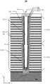
如图1示,为本发明提供的一种正常结构下的由双堆叠结构构成的,在制造阶段的示例性3D存储器100的截面,该制造阶段用于形成在衬底102上方垂直延伸穿过双堆叠结构104(包括下堆叠结构104A和上堆叠结构104B)的NAND存储器串110。下堆叠结构104A和上堆叠结构104B中的每一个包括多个电介质层对,每电介质层对包括牺牲层106(例如,氮化物)和电介质层108(例如,氧化物)。一旦完成如图1中存储器串110的所有制造过程,通过栅极替换工艺用存储器叠层(例如,金属)替换堆叠结构104,其用导电层替换每个牺牲层106。NAND存储器串110包括分别穿过下堆叠结构104A和上堆叠结构104B形成的下沟道结构112A和上沟道结构112B。NAND存储器串110还包括位于其下端的半导体插塞114和位于其上端的沟道插塞116。如图1所示,半导体插塞114延伸到衬底102的一部分中,即在衬底102的顶表面下方。As shown in FIG. 1 , a cross-section of an
下沟道结构112A和上沟道结构112B(统称为“沟道结构”112)包括沿其侧壁和在其底表面上的存储膜118和半导体沟道120。为了使半导体沟道120接触存储膜118下面的半导体插塞114,需要执行深孔打穿刻蚀(也被称为SONO穿孔工艺)以刻蚀穿过在下沟道结构112A的底表面上形成的存储膜118,所述存储膜118包括阻挡层122、储存层124(例如Si3N4)和隧穿层126(例如SiO2)。由于深孔打穿刻蚀使用高能刻蚀剂等离子体,因此对于上沟道结构112B和下沟道结构112A存在窄工艺裕度(例如,小于10nm)以在其接合位置处叠置(overlay)从而避免在接合位置处的侧壁损坏和/或底表面上的刻蚀不足(under-etch)。
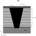
然而,实际情况则是,由于晶圆自身的翘曲、对准精准度等影响因素存在,还是会存在如图2所示的无法准确对准问题发生,从而造成下沟道结构112A和上沟道结构112B在衔接处发生衔接位置错位。会在刻蚀穿过底部存储膜118抵达半导体插塞114过程中,造成如图2所示的虚线区域的侧壁磨损。直接原因是下沟道结构112A和上沟道结构112B在衔接处发生衔接位置错位,使得部分侧壁暴露在了“SONO穿孔”工艺的刻蚀通道中。现有技术中,却存在堆叠层数达到一定值后,对晶圆扫明场像(Bright Field Image,简写为:BFI),无法发现相应的下堆叠结构上侧壁磨损的问题。However, the actual situation is that due to the influence factors such as the warpage of the wafer itself, alignment accuracy, etc., the problem of inaccurate alignment as shown in FIG. 2 will still occur, resulting in the
所述深孔打穿刻蚀包括:干法刻蚀工艺沿沟道孔119竖直方向刻蚀沟道孔119底部的存储膜118,以使半导体插塞114(也被描述为外延结构)暴露出;通常在进行所述干法刻蚀工艺之前,会在存储膜118表面沉积一层非晶硅(α-Si)保护层,并在刻蚀完后,去除沟道孔119侧壁上的非晶硅保护层;之后再生长所述半导体沟道120。The deep hole punching etching includes: a dry etching process etches the
为了使本发明的目的、技术方案及优点更加清楚明白,以下结合附图及实施例,对本发明进行进一步详细说明。应当理解,此处所描述的具体实施例仅仅用以解释本发明,并不用于限定本发明。In order to make the objectives, technical solutions and advantages of the present invention clearer, the present invention will be further described in detail below with reference to the accompanying drawings and embodiments. It should be understood that the specific embodiments described herein are only used to explain the present invention, but not to limit the present invention.
实施例1:Embodiment 1:
本发明实施例1提供了一种双堆叠结构中检测沟道孔侧壁刻蚀损伤的方法,如图3所示,包括:Embodiment 1 of the present invention provides a method for detecting etching damage to the sidewall of a channel hole in a dual stack structure, as shown in FIG. 3 , including:
在步骤202中,刻蚀出辅助沟道孔结构;其中,所述辅助沟道孔的深度与上堆叠结构中的堆叠结构厚度偏差在预设范围内。In
其中,所述辅助沟道孔结构生成的作用就是帮助去除上沟道结构和上堆叠结构,因此,将其命名为辅助沟道孔结构。在实现过程中,所述辅助沟道孔结构具有多种选择方案,包括:The role of the auxiliary channel hole structure is to help remove the upper channel structure and the upper stack structure, so it is named as the auxiliary channel hole structure. In the implementation process, the auxiliary channel hole structure has various options, including:
方式一、进行前栅自对准结构光刻;方式二、后栅自对准结构光刻;方式三、栅线缝隙;方式四、定制化图形的栅对准光刻。上述四种方式中的前三种,复用了已有存储区的相关沟道孔/沟槽工艺(包括光刻图形),而方式四则采用定制化图形方式,跳出已有的相关沟道孔/沟槽工艺,从而进一步改善检测效率,因为去除上堆叠结构对于半导体结构来说就是破坏性的,因此,所述定制化图形可以是条形、圆形、方形等等,通常会根据已经制作的沟道孔结构进行布局,而其形状大小和密集程度,可在考虑效率的情况下制作的比前三种方式规模更大。The first method is to perform the self-aligned structure lithography of the front grid; the second method is to perform the self-aligned structure lithography of the rear grid; the third method is to perform the grid line gap; The first three of the above four methods reuse the relevant channel hole/trench process (including lithography patterns) of the existing storage area, while the fourth method uses a customized pattern to jump out of the existing relevant channel holes. /trench process, thereby further improving the detection efficiency, because removing the upper stack structure is destructive to the semiconductor structure, therefore, the customized pattern can be strip, circle, square, etc., usually according to the already fabricated The layout of the channel hole structure, and its shape, size and density can be made larger than the first three methods in consideration of efficiency.
上述四种方式共同特点是,它们所制作得到沟道孔或沟槽所在区域是上堆叠结构104B区域;由此,也可以已知悉,方式二相比较方式一而言,同样数量沟道孔情况下,其得到的辅助沟道孔结构对应执行后续步骤203来说,相应完成步骤203的效率更高。The common feature of the above four methods is that the area where the channel holes or trenches are produced is the area of the
其中,所述偏差在预设范围内,具体在上堆叠结构和下堆叠结构之间不包含刻蚀停止层时,通常设定辅助沟道孔结构厚度要达到上堆叠结构自身厚度,并且超出的厚度范围要控制在1-3个介质层的厚度或者牺牲层的厚度内。而在上堆叠结构和下堆叠结构之间包括刻蚀停止层时,通常设定辅助沟道孔结构厚度要达到所述刻蚀停止层,且达到所述刻蚀停止层的部分不超过所述刻蚀停止层厚度。The deviation is within a preset range. Specifically, when an etch stop layer is not included between the upper stack structure and the lower stack structure, the thickness of the auxiliary channel hole structure is usually set to reach the thickness of the upper stack structure itself, and the excess The thickness range should be controlled within the thickness of 1-3 dielectric layers or the thickness of the sacrificial layer. When an etch stop layer is included between the upper stack structure and the lower stack structure, the thickness of the auxiliary channel hole structure is usually set to reach the etch stop layer, and the part reaching the etch stop layer does not exceed the etch stop layer. Etch stop layer thickness.
在步骤203中,通过所述辅助沟道孔结构,刻蚀掉位于下堆叠结构以上的上堆叠结构,露出可供检测的下沟道结构中的存储膜;其中,所述下沟道结构位于所述下堆叠结构中。In
其中,在步骤203中所描述的所述下堆叠结构以上的上堆叠结构,尤其指代的是上述布局有包含存储膜的沟道结构的上堆叠结构区域。也就是说,除了布局有包含存储膜的沟道结构以外的上堆叠结构区域,是否被刻蚀掉并不影响本发明实施例方法的完整实现。Wherein, the upper stack structure above the lower stack structure described in
在步骤204中,检测所述下沟道结构中的存储膜的侧壁轮廓。In
优选的是采用晶圆扫明场像,获取所述下沟道结构中存储膜的侧壁轮廓以检测侧壁损伤情况。Preferably, a wafer scanning bright field image is used to obtain the sidewall profile of the storage film in the lower channel structure to detect sidewall damage.
本发明实施例选择了影响沟道孔侧壁结构完整性的关键步骤,并设计了一套不仅能够去除上沟道结构,露出可供检测的下沟道结构中的存储膜,而且,还能够保持整个过程不至于破坏下沟道结构中的存储膜,使得在双堆叠结构中检测沟道孔侧壁刻蚀损伤成为了可能,并且还能达到检测准确度的要求(即下沟道结构的存储膜不被破坏)。The embodiment of the present invention selects the key steps that affect the structural integrity of the sidewall of the channel hole, and designs a set that can not only remove the upper channel structure and expose the storage film in the lower channel structure for detection, but also can Keeping the whole process not to damage the storage film in the lower channel structure makes it possible to detect the etching damage of the sidewall of the channel hole in the double stack structure, and can also meet the requirements of detection accuracy (that is, the The storage film is not damaged).
结合本发明实施例,对于上述通过所述辅助沟道孔结构,刻蚀掉位于下堆叠结构以上的上堆叠结构,至少存在两种可选的实现方式,接下来将分别以实现方式一和实现方式二加以区别称呼。With reference to the embodiments of the present invention, for the above-mentioned upper stack structure above the lower stack structure to be etched away through the auxiliary channel hole structure, there are at least two optional implementations, and the following will be respectively implemented in the first and second implementations. The second method is called differently.
在实现方式一中,具体表现为首先在步骤202之前还包括以下步骤201,如图4所示,在所述步骤201中包括:In implementation manner 1, the specific performance is that the following
获取对存储膜完成深孔打穿刻蚀的半导体结构,对于沟道孔内的存储膜表面沉积保护层。A semiconductor structure with deep hole punch-through etching for the storage film is obtained, and a protective layer is deposited on the surface of the storage film in the channel hole.
其中,存储膜在业内也被描述为ONO(全称为:OXIDE NITRIDE OXIDE)结构;所述深孔打穿刻蚀也被描述为SONO穿孔工艺;所述沟道孔内的存储膜表面沉积保护层的意义在于,保护可能受损伤的侧壁形貌。Among them, the storage film is also described as an ONO (full name: OXIDE NITRIDE OXIDE) structure in the industry; the deep hole punching and etching is also described as a SONO perforation process; a protective layer is deposited on the surface of the storage film in the channel hole The significance is to protect the sidewall topography that may be damaged.
其中,所述保护层材料具体为无定型硅、氧化硅、多晶硅中的一种或者多种,例如7nm的非晶硅。除此以外,所述保护层材料还可以是其他材料,但是,需要保证至少存在一种刻蚀工艺,能够使得所述保护层所选择的材料与电介质层108的选择比,要与该刻蚀工艺下牺牲层106与电介质层108的选择比近似或者更高。Wherein, the protective layer material is specifically one or more of amorphous silicon, silicon oxide, and polysilicon, for example, 7nm amorphous silicon. In addition to this, the protective layer material can also be other materials, but it needs to ensure that there is at least one etching process, which can make the selection ratio of the material selected for the protective layer and the
其次,在方式一中,对应的步骤203中的特征内容“通过所述辅助沟道孔结构,刻蚀掉位于下堆叠结构以上的上堆叠结构”具体实现为:Secondly, in the first mode, the corresponding feature content in
利用电介质层和牺牲层选择比,以及电介质层和保护层选择比均满足预设条件的刻蚀工艺,刻蚀掉位于下堆叠结构最上层牺牲层以上的堆叠结构,露出可供检测的下沟道结构中的存储膜。Using the etching process in which the selection ratio of the dielectric layer and the sacrificial layer and the selection ratio of the dielectric layer and the protective layer meet the preset conditions, the stack structure above the uppermost sacrificial layer of the lower stack structure is etched away, and the lower trench for detection is exposed. storage membrane in the channel structure.
其核心原理就在于,利用特定的刻蚀工艺,能够保证对牺牲层和保护层刻蚀速率远低于对电介质层的刻蚀速率,从而能够刻蚀掉位于下堆叠结构最上层牺牲层以上的堆叠结构,露出可供检测的下沟道结构的存储膜(ONO结构)。例如:采用湿法刻蚀工艺中,使用浓度为40%-60%的氢氟酸进行刻蚀(优选的为49%浓度),最终能够获得如图14所示的效果图。在具体实现过程中,还可以是包含其它刻蚀液成分的氢氟酸混合溶液。The core principle is that the specific etching process can ensure that the etching rate of the sacrificial layer and the protective layer is much lower than the etching rate of the dielectric layer, so that the uppermost sacrificial layer of the lower stack structure can be etched away. The stacked structure exposes the memory film (ONO structure) of the lower channel structure for detection. For example, in the wet etching process, use hydrofluoric acid with a concentration of 40%-60% for etching (preferably a concentration of 49%), and finally the effect diagram shown in FIG. 14 can be obtained. In a specific implementation process, it may also be a hydrofluoric acid mixed solution containing other etching solution components.
在不同的场景中,考虑到加工生产线的完整性,所述存储膜表面在进行深孔打穿刻蚀前生成有保护用的表层(如图2所示的半导体沟道120),则所述获取对存储膜完成深孔打穿刻蚀的半导体结构,还包括:移除存储膜表面上起深孔打穿刻蚀过程保护用的表层,得到存储膜侧壁的轮廓。在该场景中,之所以要移除存储膜上起保护用的表层,是为了避免在深孔打穿刻蚀过程中仅存储膜上的表层受到损伤,而存储膜的轮廓还是完整,此时,若不移除存储膜上的表层,而直接在存储膜上的表层上沉积保护层,形成了存储膜上的表层的图形(而非实际的存储膜的轮廓图形),就会造成ONO受到损伤的误判结果(因为,此时的图形是源自所述起保护作用的表层的轮廓而并非存储膜的轮廓)。In different scenarios, considering the integrity of the processing line, a protective surface layer (the semiconductor channel 120 shown in FIG. 2 ) is formed on the surface of the storage film before deep hole punching is performed, then The obtaining of the semiconductor structure on which the deep hole punch-through etching is performed on the storage film further includes: removing the surface layer used for the protection of the deep hole punch-through etching process on the surface of the storage film to obtain the outline of the sidewall of the storage film. In this scenario, the reason for removing the protective surface layer on the storage film is to avoid damage to only the surface layer on the storage film during the deep hole punching and etching process, while the outline of the storage film is still intact. , if the surface layer on the storage film is not removed, but a protective layer is directly deposited on the surface layer on the storage film, forming a pattern of the surface layer on the storage film (rather than the actual outline pattern of the storage film), which will cause ONO to suffer Misjudgment results of damage (because the pattern at this time is derived from the contour of the protective surface layer and not the contour of the storage film).
相比较方式一而言,方式二则在操作步骤上显得更为简洁,所述通过所述辅助沟道孔结构,刻蚀掉位于下堆叠结构以上的上堆叠结构,具体实现为:利用电介质层和牺牲层选择比满足预设条件的刻蚀工艺;通过控制刻蚀时间,使得上堆叠层中的电介质层刚好被刻蚀掉。但是,相比较方式一而言,方式二自身的刻蚀控制精确度和难度相比较方式一而言更高。具体采用哪种方式可以根据实际工艺水平和生产加工周期综合考虑后进行选择。由于存在后续扩展方案中,使用的超声处理,因此,此处刻蚀时间的控制上也是允许有一定的偏差,即在控制刻蚀时间上,还可以遗留部分上堆叠层的存储膜,并通过后续的超声处理来配合去除。Compared with the first method, the second method is more concise in operation steps. The upper stack structure located above the lower stack structure is etched away through the auxiliary channel hole structure. The specific implementation is as follows: using a dielectric layer The selection ratio of the sacrificial layer and the sacrificial layer satisfies the etching process of the preset condition; by controlling the etching time, the dielectric layer in the upper stack layer is just etched away. However, compared with the first method, the etching control accuracy and difficulty of the second method are higher than that of the first method. Which method to use can be selected after comprehensive consideration of the actual process level and production and processing cycle. Due to the ultrasonic treatment used in the subsequent expansion scheme, a certain deviation is allowed in the control of the etching time. Subsequent sonication to accompany the removal.
在已有的双堆叠结构中,通常会在所述上堆叠结构和下堆叠结构之间沉积有刻蚀停止层,在现有技术中,例如专利CN109496355A公开的,其“刻蚀停止层208可包括金属,例如W、Co、Cu、Al或其任何组合。在一个示例中,刻蚀停止层208是钨层。刻蚀停止层208还可以包括半导体,例如多晶硅、非晶硅、硅化物或其任何组合。刻蚀停止层208可以包括与形成电介质层205的材料(例如,氧化硅)不同的任何其他合适的材料和由导电层203替换的另一种类型的电介质层(例如,氮化硅)。刻蚀停止层208的厚度可以在约20nm和约30nm之间,例如在20nm和30nm之间(例如,20nm、21nm、22nm、23nm、24nm、25nm、26nm、27nm、28nm、29nm、30nm,由这些值中的任何一个为下端界定的任何范围,或由这些值中的任何两个限定的任何范围)”然而,要完成本发明实施例1所提出的方案,除了可以选择上述结构以外,本发明实施例还提供了一种优选的实现方案,具体的:采用预设厚度的电介质层构成,所述预设厚度具体为:位于区间[25nm,200nm]中,例如100nm。本发明实施例采用上述优选实现方案,可以保证刻蚀停止层在执行步骤203过程中一并被刻蚀掉,从而能够将下沟道结构中的存储膜完整的展现出来,而除此以外的步骤或多或少需要增加去除刻蚀停止层的附加步骤,影响了整个检测过程的效率。在本发明实施例中,对于上堆叠结构和下堆叠结构之间存在刻蚀停止层的情况下,所述刻蚀停止层也是要被一并刻蚀掉的,这样暴露出来的才是下堆叠结构最表层牺牲层,才是完整下沟道结构。因为,刻蚀停止层314在产生上沟道孔和下沟道孔偏移时,如图9所示,会覆盖部分偏移部分,影响最后的图片采集的。In the existing dual stack structure, an etch stop layer is usually deposited between the upper stack structure and the lower stack structure. In the prior art, such as disclosed in patent CN109496355A, the “etch stop layer 208 Includes metals such as W, Co, Cu, Al, or any combination thereof. In one example, etch stop layer 208 is a tungsten layer. Etch stop layer 208 may also include semiconductors such as polysilicon, amorphous silicon, silicide or Any combination thereof. Etch stop layer 208 may comprise any other suitable material different from the material forming dielectric layer 205 (eg, silicon oxide) and another type of dielectric layer (eg, nitrided) replaced by
结合本发明实施例,为了进一步提高保留的下沟道结构的完整性,并考虑本发明实施例中刻蚀掉上堆叠结构的原理,优选的,所述下沟道结构周围的堆叠结构的上表面层(与上沟道结构相邻)为牺牲层。由于,本发明实施例所提出的方案,会在刻蚀上堆叠结构过程中,停止在辅助沟道孔结构底部最先遇到的牺牲层(即下沟道结构周围的堆叠结构的上表面牺牲层)上,因此,上述优选的方案可以更精准的保留下沟道孔中的存储膜。With reference to the embodiment of the present invention, in order to further improve the integrity of the remaining lower channel structure, and considering the principle of etching away the upper stack structure in the embodiment of the present invention, preferably, the upper portion of the stack structure around the lower channel structure is The surface layer (adjacent to the upper channel structure) is the sacrificial layer. Because, the solution proposed by the embodiment of the present invention stops at the sacrificial layer first encountered at the bottom of the auxiliary channel hole structure (that is, the sacrificial layer on the upper surface of the stack structure around the lower channel structure) during the etching process of the upper stack structure. layer), therefore, the above preferred solution can more accurately retain the storage film in the lower channel hole.
直接采用步骤203中所描述的内容,最后可能执行完后呈现如图13的结构示意图。虽然,可以将所述保护层沉积的很薄,但是,出于刻蚀过程中保守考虑,或多或少还会存在保护层和/或存储膜的残留,因此,排除手动去除的可选方式以外,结合本发明实施例还采用了一种优选的实现方式,可以提高去除的安全性和效率。优选方式体现为:在刻蚀的过程中或者刻蚀结束后,使用超声处理,以便去除掉在所述刻蚀过程中,仍然遗留下来的位于上沟道结构的保护层和/或存储膜。最终的效果图如图14所示,其中突兀在下沟道结构以外的保护层在超声作用下自然脱落。The content described in
基于本发明实施例已经得到的如图14所示的结构图,此时可以通过晶圆扫明场像,获取所述下沟道结构中存储膜的侧壁轮廓以检测侧壁损伤情况。以图15为例,如果下沟道结构侧壁的存储膜存在损伤,则相应的图15所示损伤结果的拍摄效果图如图16所示,当中间区域中出现不规则的图形330,则可认定存储膜受到了损伤。Based on the structure diagram shown in FIG. 14 that has been obtained in the embodiment of the present invention, the sidewall profile of the storage film in the lower channel structure can be acquired by scanning the field image of the wafer to detect sidewall damage. Taking FIG. 15 as an example, if there is damage to the storage film on the sidewall of the lower channel structure, the corresponding photographing effect diagram of the damage result shown in FIG. 15 is shown in FIG. 16 . When an
本发明实施例所提出的方案尤其适用于,所述双堆叠结构中堆叠结构的层数为96、128、160或者256,甚至更高层数场景。The solutions proposed in the embodiments of the present invention are especially applicable to scenarios where the number of layers of the stacked structure in the double-stacked structure is 96, 128, 160, or 256, or even higher.
实施例2:Embodiment 2:
图5-图16示出了根据本发明实施例1实现方法,且以实施例1中的方式一作为手段,在一典型的双堆叠结构的3D存储器加工过程中的示例实现过程。在本发明实施例中将如图实施例1中相关方法步骤,并且,会基于本发明实施例的特性实现环境,进行必要的扩展约束。需要说明书的是,本发明实施例是为了更好的展示实施例1中部分实施方式在特定场景下的实现而做到更为详尽的描述,因此,不应当作为本发明可获得保护范围的限缩依据。在本发明实施例中,深孔打穿刻蚀被称为SONO穿孔工艺,而存储膜则被描述为ONO结构。FIGS. 5-16 show an example implementation process in a typical double-stack structure 3D memory processing process by using the method 1 in the embodiment 1 as a means according to the implementation method according to Embodiment 1 of the present invention. In this embodiment of the present invention, the relevant method steps shown in Embodiment 1 will be shown, and necessary expansion constraints will be implemented based on the characteristic implementation environment of the embodiment of the present invention. It should be noted that the embodiments of the present invention are described in more detail in order to better demonstrate the implementation of some of the implementations in Embodiment 1 under specific scenarios. Therefore, it should not be taken as a limitation of the obtainable protection scope of the present invention. abbreviated basis. In the embodiment of the present invention, the deep hole punching etching is called a SONO through-hole process, and the storage film is described as an ONO structure.
在衬底上形成第一堆叠结构。衬底可以是硅衬底。第一堆叠结构可包括多个交错的牺牲层和电介质层。参考图5,在硅衬底302的正面上形成包括多对第一电介质层308和第二电介质层(也被称为“牺牲层”)306的第一堆叠结构304A(即实施例1中的下堆叠结构)。在一些实施例中,通过在形成第一堆叠结构304A之前在硅衬底302上沉积诸如氧化硅的电介质材料或热氧化,在第一堆叠结构304A和硅衬底302之间形成绝缘层303。根据一些实施例,第一堆叠结构304A包括交错的牺牲层306和电介质层308。可替换地,可以在硅衬底302上沉积电介质层308和牺牲层306,以形成第一堆叠结构304A。在一些实施例中,每个电介质层308包括氧化硅层,并且每个牺牲层306包括氮化硅层。第一堆叠结构304A可以通过一种或多种薄膜沉积工艺形成,包括但不限于化学气相沉积(Chemical Vapor Deposition,简写为:CVD)、物理气相沉积(Physical Vapor Deposition,简写为:PVD)、原子层沉积(AtomicLayer Deposition,简写为:ALD)或其任何组合。A first stack structure is formed on the substrate. The substrate may be a silicon substrate. The first stack structure may include a plurality of interleaved sacrificial layers and dielectric layers. Referring to FIG. 5 , a
如图5所示,第一沟道孔310A(即实施例1中的下沟道孔)是垂直延伸穿过第一堆叠结构304A形成的开口。在一些实施例中,穿过第一堆叠结构304A形成多个开口,使得每个开口成为在后面的过程中形成个体NAND存储器串的位置。在一些实施例中,用于形成第一沟道孔310A的制造工艺包括湿法刻蚀和/或干法刻蚀,例如深度离子反应刻蚀(DeepReactive Ion Etching,简写为:DRIE)。As shown in FIG. 5 , the
在一些实施例中,第一沟道孔310A进一步延伸到硅衬底302的顶部中以形成第一沟道孔310A的开槽311。穿过第一堆叠结构304A的刻蚀过程可以不在硅衬底302的顶表面处停止并且可以继续刻蚀硅衬底302的一部分。在一些实施例中,在刻蚀穿过第一堆叠结构304A之后,使用单独的刻蚀工艺来刻蚀硅衬底302的一部分以形成开槽311。如下面详细描述的,第一沟道孔310A的开槽311的深度大于穿过硅衬底302的任何其他结构的开槽,例如狭缝开口和触点开口,以确保后面的背面衬底减薄工艺不会损坏其他结构。In some embodiments, the
如图6中所示,使用一个或多个薄膜沉积工艺(例如PVD、CVD、ALD、电镀、无电镀或其任何组合)沉积牺牲结构312,以部分或完全填充第一沟道孔310A(包括开槽311,如图5所示)。牺牲结构312可包括在后续工艺中去除的任何合适材料,例如多晶硅、碳、光致抗蚀剂等。在一些实施例中,使用化学机械抛光(Chemical Mechanical Polishing,简写为:CMP)工艺平面化牺牲结构312以使其顶表面与第一堆叠结构304A的顶表面齐平。As shown in FIG. 6, a
如图7中所示,在第一堆叠结构层304A和牺牲结构312上形成刻蚀停止层314,以完全覆盖第一堆叠结构层304A和牺牲结构312。在本实施例中,所述刻蚀停止层314与电介质层308选用同样材料,并控制沉积厚度为100埃。此处,之所以选择100埃参数,是因为选择了电介质层材料作为刻蚀停止层314是为了便于后续去除第二堆叠解耦股304B时,容易选择腐蚀液(需要考虑的刻蚀选择比对象少了,也就容易选择腐蚀液了);那么其在制作上沟道孔310B结构时,本身也会被腐蚀掉,因此,其厚度不宜选择的太薄。As shown in FIG. 7 , an
参考图8,在第一堆叠结构304A上方的刻蚀停止层314上形成包括多个电介质层对的第二堆叠结构304B。第二堆叠结构304B可以通过一种或多种薄膜沉积工艺形成,包括但不限于CVD、PVD、ALD或其任何组合。Referring to FIG. 8, a
如图8所示,第二沟道孔310B是形成为垂直穿过第二堆叠结构304B延伸直到被刻蚀停止层314停止的另一个开口。第二沟道孔310B可以与第一沟道孔310A(图5中所示)对准,以便与第一沟道孔310A的至少一部分叠置,使得一旦去除牺牲结构312,就可以连接第一沟道孔310A和第二沟道孔310B。在一些实施例中,用于形成第二沟道孔310B的制造工艺包括湿法刻蚀和/或干法刻蚀,例如DRIE。因为刻蚀停止层314可以保护第一堆叠结构304A的结构免受由于第二沟道孔310B的刻蚀而造成的损坏。As shown in FIG. 8 , the
如图9中所示,例如使用干法刻蚀和/或湿法刻蚀工艺去除其中叠置第一开口310A和第二开口310B的刻蚀停止层314的一部分。由于各向同性刻蚀(例如,通过湿法刻蚀)而可以回刻蚀所述刻蚀停止层314的附加部分(未示出)。一旦去除了刻蚀停止层314的一部分,就可以从第二沟道孔310B暴露牺牲结构312(图8中所示)。如图9所示,通过湿法刻蚀和/或干法刻蚀工艺在第一堆叠结构304A中去除牺牲结构312。在去除牺牲结构312之后,第一沟道孔310A再次开放并与第二沟道孔310B连接以形成沟道孔310,如图9所示,其垂直延伸穿过第一堆叠结构304A和第二堆叠结构304B以及刻蚀停止层314。As shown in FIG. 9 , a portion of the
如图10所示,先在沟道孔310制作半导体插塞315,并沿沟道孔310的侧壁和半导体插塞315的表面形成存储膜318(包括阻挡层322、储存层324和隧穿层326)和半导体沟道320。在一些实施例中,首先沿沟道孔310的侧壁和底表面沉积存储膜318,然后在存储膜318上方沉积半导体沟道320。具体,可以使用一个或多个薄膜沉积工艺(例如ALD、CVD、PVD、任何其他合适的工艺或其任何组合)依次沉积阻挡层322、储存层324和隧穿层326,以形成存储膜318。然后可以通过使用一个或多个薄膜沉积工艺(例如ALD、CVD、PVD、任何其他合适的工艺或其任何组合)在隧穿层326上沉积多晶硅或任何其他合适的半导体材料来形成半导体沟道320。As shown in FIG. 10 , a
如图10所示,存储膜318和半导体沟道320可以覆盖沟道孔310的底表面和侧壁两者。在一些实施例中,随后沉积氧化硅层、氮化硅层、氧化硅层和多晶硅层(一起构成“ONO结构”,其中所述多晶硅层即实施例1所述的存储膜表面上形成用于在SONO穿孔工艺中保护存储膜的表层)以形成存储膜318和半导体沟道320。As shown in FIG. 10 , the
如图11中所示,执行SONO穿孔工艺以刻蚀穿过在第一沟道孔310A的底表面上形成的存储膜318,所述存储膜318包括阻挡层322、储存层324(例如Si3N4)和隧穿层326(例如SiO2)。在一些实施例中,通过CMP、湿法刻蚀和/或干法刻蚀去除并平面化存储膜318、半导体沟道320和覆盖层A326A的位于第二堆叠结构304B的顶表面上的部分。As shown in FIG. 11 , a SONO via process is performed to etch through the
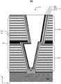
如图12中所示,在沟道孔310内部,位于存储膜318或者半导体沟道320表面沉积保护层328,所述保护层328采用和牺牲层306相同的材料制作,使用湿法刻蚀和/或干法刻蚀工艺(例如DRIE)穿过电介质叠层304B形成狭缝开口316(例如,栅极线狭缝)或者沟道孔(例如第二沟道孔301B),并停止在刻蚀停止层314。在本发明实施例中,对于上堆叠结构和下堆叠结构之间存在刻蚀停止层的情况下,所述刻蚀停止层也是要被一并刻蚀掉的,这样暴露出来的是下堆叠结构最表层的牺牲层,此时才是完整下沟道结构。因为,刻蚀停止层314在产生上沟道孔和下沟道孔偏移时,如图9所示,会覆盖部分偏移部分,影响最后的图片采集的。As shown in FIG. 12 , inside the
如图13所示,例如使用浓度为49%的氢氟酸进行湿法刻蚀。所述氢氟酸对于介质层308和牺牲层306之间具有高选择比,并且,所述氢氟酸对于刻蚀停止层314和保护层328之间也具有高选择比。从而将3D存储器300浸泡在浓度为49%的氢氟酸中时,能够得到如图13的刻蚀效果;此时,在刻蚀的同时使用超声处理,通过振动去掉如图13所示的暴露在第一堆叠结构304A之上的保护层材料,得到如图14所示的效果图。在上述图5-图14中,并未去刻意的呈现,若第一沟道孔中的侧壁SONO结构受到刻蚀损伤时的效果,于是,在本实施例中特意补充了说明书附图15和附图16来呈现上述存在刻蚀损伤时的第一沟道孔中的结构示意图,和进一步通过晶圆扫明场像得到的检测结果示意图。As shown in FIG. 13 , for example, wet etching is performed using hydrofluoric acid having a concentration of 49%. The hydrofluoric acid has a high selectivity ratio between the dielectric layer 308 and the
通过图15不难发现,一旦第一沟道孔中的侧壁ONO结构受到刻蚀损伤,则在衬底保护层的时候,便会表现出表面的凹槽特性,并且在通过晶圆扫明场像时,呈现出如图16中330所标注的不协调的图案效果;需要指出的是,图16中的图案效果仅仅是一种示意性呈现,实际的效果可能比这更复杂,但是,共性的特点是:一旦受到了刻蚀损伤,则形成一个或者多个凹槽图案是主要的表征形式。It is not difficult to find from Fig. 15 that once the sidewall ONO structure in the first channel hole is etched and damaged, the surface groove characteristics will be exhibited when the substrate protective layer is formed, and when the surface is scanned through the wafer When a field image is displayed, an uncoordinated pattern effect as marked by 330 in Figure 16 is presented; it should be pointed out that the pattern effect in Figure 16 is only a schematic presentation, and the actual effect may be more complicated than this, but, The common feature is that once it is damaged by etching, the formation of one or more groove patterns is the main characterization form.
以上所述仅为本发明的较佳实施例而已,并不用以限制本发明,凡在本发明的精神和原则之内所作的任何修改、等同替换和改进等,均应包含在本发明的保护范围之内。The above descriptions are only preferred embodiments of the present invention and are not intended to limit the present invention. Any modifications, equivalent replacements and improvements made within the spirit and principles of the present invention shall be included in the protection of the present invention. within the range.
Claims (13)
Priority Applications (1)
| Application Number | Priority Date | Filing Date | Title |
|---|---|---|---|
| CN201910863980.0ACN110634760B (en) | 2019-09-12 | 2019-09-12 | Method for detecting etching damage of side wall of channel hole in double-stack structure |
Applications Claiming Priority (1)
| Application Number | Priority Date | Filing Date | Title |
|---|---|---|---|
| CN201910863980.0ACN110634760B (en) | 2019-09-12 | 2019-09-12 | Method for detecting etching damage of side wall of channel hole in double-stack structure |
Publications (2)
| Publication Number | Publication Date |
|---|---|
| CN110634760A CN110634760A (en) | 2019-12-31 |
| CN110634760Btrue CN110634760B (en) | 2022-04-15 |
Family
ID=68972763
Family Applications (1)
| Application Number | Title | Priority Date | Filing Date |
|---|---|---|---|
| CN201910863980.0AActiveCN110634760B (en) | 2019-09-12 | 2019-09-12 | Method for detecting etching damage of side wall of channel hole in double-stack structure |
Country Status (1)
| Country | Link |
|---|---|
| CN (1) | CN110634760B (en) |
Families Citing this family (6)
| Publication number | Priority date | Publication date | Assignee | Title |
|---|---|---|---|---|
| CN111244102A (en)* | 2020-01-16 | 2020-06-05 | 长江存储科技有限责任公司 | Three-dimensional memory and preparation method thereof |
| CN111323443B (en)* | 2020-03-04 | 2023-12-01 | 武汉新芯集成电路制造有限公司 | SONO etching sample preparation and detection method |
| CN111640761B (en)* | 2020-06-09 | 2021-06-22 | 长江存储科技有限责任公司 | How to make a three-dimensional memory |
| CN111653496B (en)* | 2020-06-11 | 2021-04-27 | 长江存储科技有限责任公司 | Method for detecting etch defects in channel structures |
| CN112289803A (en)* | 2020-10-22 | 2021-01-29 | 长江存储科技有限责任公司 | 3D memory device and its manufacturing method |
| CN114623777B (en)* | 2022-02-21 | 2022-11-18 | 武汉大学 | A measurement model construction method and measurement method for a stacked nanosheet structure |
Citations (4)
| Publication number | Priority date | Publication date | Assignee | Title |
|---|---|---|---|---|
| US20150311301A1 (en)* | 2010-03-26 | 2015-10-29 | Kwang Soo SEOL | Three-dimensional semiconductor memory devices and methods of fabricating the same |
| CN107863305A (en)* | 2017-11-21 | 2018-03-30 | 长江存储科技有限责任公司 | A kind of detection method of SONO etching technics |
| CN108140643A (en)* | 2015-11-20 | 2018-06-08 | 桑迪士克科技有限责任公司 | Three-dimensional NAND device including support pedestal structure for buried source line and method of fabricating the same |
| CN109830483A (en)* | 2019-02-14 | 2019-05-31 | 长江存储科技有限责任公司 | 3D nand memory and forming method thereof |
Family Cites Families (1)
| Publication number | Priority date | Publication date | Assignee | Title |
|---|---|---|---|---|
| JP5613033B2 (en)* | 2010-05-19 | 2014-10-22 | ルネサスエレクトロニクス株式会社 | Manufacturing method of semiconductor device |
- 2019
- 2019-09-12CNCN201910863980.0Apatent/CN110634760B/enactiveActive
Patent Citations (4)
| Publication number | Priority date | Publication date | Assignee | Title |
|---|---|---|---|---|
| US20150311301A1 (en)* | 2010-03-26 | 2015-10-29 | Kwang Soo SEOL | Three-dimensional semiconductor memory devices and methods of fabricating the same |
| CN108140643A (en)* | 2015-11-20 | 2018-06-08 | 桑迪士克科技有限责任公司 | Three-dimensional NAND device including support pedestal structure for buried source line and method of fabricating the same |
| CN107863305A (en)* | 2017-11-21 | 2018-03-30 | 长江存储科技有限责任公司 | A kind of detection method of SONO etching technics |
| CN109830483A (en)* | 2019-02-14 | 2019-05-31 | 长江存储科技有限责任公司 | 3D nand memory and forming method thereof |
Also Published As
| Publication number | Publication date |
|---|---|
| CN110634760A (en) | 2019-12-31 |
Similar Documents
| Publication | Publication Date | Title |
|---|---|---|
| CN110634760B (en) | Method for detecting etching damage of side wall of channel hole in double-stack structure | |
| TWI515826B (en) | Through-layer and its manufacturing method | |
| US9799671B2 (en) | Three-dimensional integration schemes for reducing fluorine-induced electrical shorts | |
| CN108649033B (en) | Semiconductor device and method of manufacturing the same | |
| US9530785B1 (en) | Three-dimensional memory devices having a single layer channel and methods of making thereof | |
| TWI713089B (en) | Methods for forming integrated circuit structure | |
| KR100743651B1 (en) | Contact formation method of semiconductor device | |
| CN110233152B (en) | Method for forming three-dimensional memory and three-dimensional memory | |
| US8623727B2 (en) | Method for fabricating semiconductor device with buried gate | |
| CN109065547B (en) | How to make a three-dimensional memory | |
| KR100825014B1 (en) | Device Separation Method of Semiconductor Device | |
| CN108831886A (en) | 3D memory | |
| CN111785725A (en) | Method of forming three-dimensional memory | |
| CN107180832A (en) | Flash memory structure and forming method thereof | |
| US6566236B1 (en) | Gate structures with increased etch margin for self-aligned contact and the method of forming the same | |
| KR20140019705A (en) | Semiconductor device and method for fabricating the same | |
| CN111326511A (en) | Memory device and method of manufacturing the same | |
| CN104377160B (en) | Metal interconnection structure and its technology | |
| CN114975230B (en) | Semiconductor device manufacturing method and semiconductor device | |
| CN114864479A (en) | Semiconductor device and method of making the same | |
| KR100894771B1 (en) | Manufacturing Method of Flash Memory Device | |
| JP2005317736A (en) | Manufacturing method of semiconductor device | |
| CN115295528A (en) | Semiconductor device and method of manufacturing the same | |
| CN113964132B (en) | Three-dimensional memory and method for manufacturing the same | |
| CN114334816B (en) | Method for forming semiconductor structure |
Legal Events
| Date | Code | Title | Description |
|---|---|---|---|
| PB01 | Publication | ||
| PB01 | Publication | ||
| SE01 | Entry into force of request for substantive examination | ||
| SE01 | Entry into force of request for substantive examination | ||
| GR01 | Patent grant | ||
| GR01 | Patent grant |