CN110581103B - Semiconductor element and manufacturing method thereof - Google Patents
Semiconductor element and manufacturing method thereofDownload PDFInfo
- Publication number
- CN110581103B CN110581103BCN201810582040.XACN201810582040ACN110581103BCN 110581103 BCN110581103 BCN 110581103BCN 201810582040 ACN201810582040 ACN 201810582040ACN 110581103 BCN110581103 BCN 110581103B
- Authority
- CN
- China
- Prior art keywords
- bit line
- storage node
- spacer
- line structure
- node contact
- Prior art date
- Legal status (The legal status is an assumption and is not a legal conclusion. Google has not performed a legal analysis and makes no representation as to the accuracy of the status listed.)
- Active
Links
- 239000004065semiconductorSubstances0.000titleclaimsabstractdescription18
- 238000004519manufacturing processMethods0.000titleclaimsabstractdescription13
- 239000010410layerSubstances0.000claimsabstractdescription53
- 238000002955isolationMethods0.000claimsabstractdescription45
- 238000000034methodMethods0.000claimsabstractdescription24
- 239000000758substrateSubstances0.000claimsabstractdescription20
- 239000011229interlayerSubstances0.000claimsabstractdescription18
- 125000006850spacer groupChemical group0.000claimsdescription75
- 229910010271silicon carbideInorganic materials0.000claimsdescription5
- HBMJWWWQQXIZIP-UHFFFAOYSA-Nsilicon carbideChemical compound[Si+]#[C-]HBMJWWWQQXIZIP-UHFFFAOYSA-N0.000claimsdescription4
- QJGQUHMNIGDVPM-UHFFFAOYSA-Nnitrogen groupChemical group[N]QJGQUHMNIGDVPM-UHFFFAOYSA-N0.000claims2
- 230000004888barrier functionEffects0.000description8
- 238000005530etchingMethods0.000description7
- 229910052581Si3N4Inorganic materials0.000description6
- 230000002093peripheral effectEffects0.000description6
- 238000010586diagramMethods0.000description5
- 229910052751metalInorganic materials0.000description5
- 239000002184metalSubstances0.000description5
- HQVNEWCFYHHQES-UHFFFAOYSA-Nsilicon nitrideChemical compoundN12[Si]34N5[Si]62N3[Si]51N64HQVNEWCFYHHQES-UHFFFAOYSA-N0.000description5
- XUIMIQQOPSSXEZ-UHFFFAOYSA-NSiliconChemical compound[Si]XUIMIQQOPSSXEZ-UHFFFAOYSA-N0.000description4
- 238000009413insulationMethods0.000description4
- 239000000463materialSubstances0.000description4
- 229910052710siliconInorganic materials0.000description4
- 239000010703siliconSubstances0.000description4
- 239000003990capacitorSubstances0.000description3
- 239000003989dielectric materialSubstances0.000description3
- WFKWXMTUELFFGS-UHFFFAOYSA-NtungstenChemical compound[W]WFKWXMTUELFFGS-UHFFFAOYSA-N0.000description3
- 229910052721tungstenInorganic materials0.000description3
- 239000010937tungstenSubstances0.000description3
- RYGMFSIKBFXOCR-UHFFFAOYSA-NCopperChemical compound[Cu]RYGMFSIKBFXOCR-UHFFFAOYSA-N0.000description2
- XPDWGBQVDMORPB-UHFFFAOYSA-NFluoroformChemical compoundFC(F)FXPDWGBQVDMORPB-UHFFFAOYSA-N0.000description2
- VYPSYNLAJGMNEJ-UHFFFAOYSA-NSilicium dioxideChemical compoundO=[Si]=OVYPSYNLAJGMNEJ-UHFFFAOYSA-N0.000description2
- BOTDANWDWHJENH-UHFFFAOYSA-NTetraethyl orthosilicateChemical compoundCCO[Si](OCC)(OCC)OCCBOTDANWDWHJENH-UHFFFAOYSA-N0.000description2
- 229910052782aluminiumInorganic materials0.000description2
- XAGFODPZIPBFFR-UHFFFAOYSA-NaluminiumChemical compound[Al]XAGFODPZIPBFFR-UHFFFAOYSA-N0.000description2
- 239000004020conductorSubstances0.000description2
- 229910052802copperInorganic materials0.000description2
- 239000010949copperSubstances0.000description2
- 229910052814silicon oxideInorganic materials0.000description2
- LGPPATCNSOSOQH-UHFFFAOYSA-N1,1,2,3,4,4-hexafluorobuta-1,3-dieneChemical compoundFC(F)=C(F)C(F)=C(F)FLGPPATCNSOSOQH-UHFFFAOYSA-N0.000description1
- 229910000838Al alloyInorganic materials0.000description1
- VYZAMTAEIAYCRO-UHFFFAOYSA-NChromiumChemical compound[Cr]VYZAMTAEIAYCRO-UHFFFAOYSA-N0.000description1
- ZOKXTWBITQBERF-UHFFFAOYSA-NMolybdenumChemical compound[Mo]ZOKXTWBITQBERF-UHFFFAOYSA-N0.000description1
- RTAQQCXQSZGOHL-UHFFFAOYSA-NTitaniumChemical compound[Ti]RTAQQCXQSZGOHL-UHFFFAOYSA-N0.000description1
- NRTOMJZYCJJWKI-UHFFFAOYSA-NTitanium nitrideChemical compound[Ti]#NNRTOMJZYCJJWKI-UHFFFAOYSA-N0.000description1
- UMVBXBACMIOFDO-UHFFFAOYSA-N[N].[Si]Chemical compound[N].[Si]UMVBXBACMIOFDO-UHFFFAOYSA-N0.000description1
- UQZIWOQVLUASCR-UHFFFAOYSA-Nalumane;titaniumChemical compound[AlH3].[Ti]UQZIWOQVLUASCR-UHFFFAOYSA-N0.000description1
- 229910021417amorphous siliconInorganic materials0.000description1
- IVHJCRXBQPGLOV-UHFFFAOYSA-NazanylidynetungstenChemical compound[W]#NIVHJCRXBQPGLOV-UHFFFAOYSA-N0.000description1
- 229910052804chromiumInorganic materials0.000description1
- 239000011651chromiumSubstances0.000description1
- 239000000470constituentSubstances0.000description1
- 230000007547defectEffects0.000description1
- 239000011810insulating materialSubstances0.000description1
- 230000010354integrationEffects0.000description1
- 238000012986modificationMethods0.000description1
- 230000004048modificationEffects0.000description1
- 229910052750molybdenumInorganic materials0.000description1
- 239000011733molybdenumSubstances0.000description1
- 238000000206photolithographyMethods0.000description1
- 238000005498polishingMethods0.000description1
- 229910021420polycrystalline siliconInorganic materials0.000description1
- 229920005591polysiliconPolymers0.000description1
- -1silicon nitride nitrideChemical class0.000description1
- WNUPENMBHHEARK-UHFFFAOYSA-Nsilicon tungstenChemical compound[Si].[W]WNUPENMBHHEARK-UHFFFAOYSA-N0.000description1
- 239000000126substanceSubstances0.000description1
- 229910052715tantalumInorganic materials0.000description1
- GUVRBAGPIYLISA-UHFFFAOYSA-Ntantalum atomChemical compound[Ta]GUVRBAGPIYLISA-UHFFFAOYSA-N0.000description1
- MZLGASXMSKOWSE-UHFFFAOYSA-Ntantalum nitrideChemical compound[Ta]#NMZLGASXMSKOWSE-UHFFFAOYSA-N0.000description1
- 229910052719titaniumInorganic materials0.000description1
- 239000010936titaniumSubstances0.000description1
Images


Classifications
- H—ELECTRICITY
- H10—SEMICONDUCTOR DEVICES; ELECTRIC SOLID-STATE DEVICES NOT OTHERWISE PROVIDED FOR
- H10B—ELECTRONIC MEMORY DEVICES
- H10B12/00—Dynamic random access memory [DRAM] devices
- H10B12/30—DRAM devices comprising one-transistor - one-capacitor [1T-1C] memory cells
- H10B12/31—DRAM devices comprising one-transistor - one-capacitor [1T-1C] memory cells having a storage electrode stacked over the transistor
- H10B12/315—DRAM devices comprising one-transistor - one-capacitor [1T-1C] memory cells having a storage electrode stacked over the transistor with the capacitor higher than a bit line
- H—ELECTRICITY
- H01—ELECTRIC ELEMENTS
- H01L—SEMICONDUCTOR DEVICES NOT COVERED BY CLASS H10
- H01L21/00—Processes or apparatus adapted for the manufacture or treatment of semiconductor or solid state devices or of parts thereof
- H01L21/70—Manufacture or treatment of devices consisting of a plurality of solid state components formed in or on a common substrate or of parts thereof; Manufacture of integrated circuit devices or of parts thereof
- H01L21/71—Manufacture of specific parts of devices defined in group H01L21/70
- H01L21/76—Making of isolation regions between components
- H01L21/762—Dielectric regions, e.g. EPIC dielectric isolation, LOCOS; Trench refilling techniques, SOI technology, use of channel stoppers
- H—ELECTRICITY
- H10—SEMICONDUCTOR DEVICES; ELECTRIC SOLID-STATE DEVICES NOT OTHERWISE PROVIDED FOR
- H10B—ELECTRONIC MEMORY DEVICES
- H10B12/00—Dynamic random access memory [DRAM] devices
- H10B12/01—Manufacture or treatment
- H10B12/02—Manufacture or treatment for one transistor one-capacitor [1T-1C] memory cells
- H10B12/03—Making the capacitor or connections thereto
- H10B12/033—Making the capacitor or connections thereto the capacitor extending over the transistor
- H10B12/0335—Making a connection between the transistor and the capacitor, e.g. plug
- H—ELECTRICITY
- H10—SEMICONDUCTOR DEVICES; ELECTRIC SOLID-STATE DEVICES NOT OTHERWISE PROVIDED FOR
- H10B—ELECTRONIC MEMORY DEVICES
- H10B12/00—Dynamic random access memory [DRAM] devices
- H10B12/01—Manufacture or treatment
- H10B12/09—Manufacture or treatment with simultaneous manufacture of the peripheral circuit region and memory cells
- H—ELECTRICITY
- H10—SEMICONDUCTOR DEVICES; ELECTRIC SOLID-STATE DEVICES NOT OTHERWISE PROVIDED FOR
- H10B—ELECTRONIC MEMORY DEVICES
- H10B12/00—Dynamic random access memory [DRAM] devices
- H10B12/30—DRAM devices comprising one-transistor - one-capacitor [1T-1C] memory cells
- H—ELECTRICITY
- H10—SEMICONDUCTOR DEVICES; ELECTRIC SOLID-STATE DEVICES NOT OTHERWISE PROVIDED FOR
- H10B—ELECTRONIC MEMORY DEVICES
- H10B12/00—Dynamic random access memory [DRAM] devices
- H10B12/30—DRAM devices comprising one-transistor - one-capacitor [1T-1C] memory cells
- H10B12/48—Data lines or contacts therefor
- H10B12/482—Bit lines
- H—ELECTRICITY
- H10—SEMICONDUCTOR DEVICES; ELECTRIC SOLID-STATE DEVICES NOT OTHERWISE PROVIDED FOR
- H10B—ELECTRONIC MEMORY DEVICES
- H10B12/00—Dynamic random access memory [DRAM] devices
- H10B12/30—DRAM devices comprising one-transistor - one-capacitor [1T-1C] memory cells
- H10B12/48—Data lines or contacts therefor
- H10B12/485—Bit line contacts
- H—ELECTRICITY
- H10—SEMICONDUCTOR DEVICES; ELECTRIC SOLID-STATE DEVICES NOT OTHERWISE PROVIDED FOR
- H10B—ELECTRONIC MEMORY DEVICES
- H10B12/00—Dynamic random access memory [DRAM] devices
- H10B12/30—DRAM devices comprising one-transistor - one-capacitor [1T-1C] memory cells
- H10B12/48—Data lines or contacts therefor
- H10B12/488—Word lines
- H—ELECTRICITY
- H10—SEMICONDUCTOR DEVICES; ELECTRIC SOLID-STATE DEVICES NOT OTHERWISE PROVIDED FOR
- H10B—ELECTRONIC MEMORY DEVICES
- H10B12/00—Dynamic random access memory [DRAM] devices
- H10B12/50—Peripheral circuit region structures
Landscapes
- Engineering & Computer Science (AREA)
- Manufacturing & Machinery (AREA)
- Physics & Mathematics (AREA)
- Condensed Matter Physics & Semiconductors (AREA)
- General Physics & Mathematics (AREA)
- Computer Hardware Design (AREA)
- Microelectronics & Electronic Packaging (AREA)
- Power Engineering (AREA)
- Semiconductor Memories (AREA)
- Internal Circuitry In Semiconductor Integrated Circuit Devices (AREA)
Abstract
Description
Translated fromChinese技术领域technical field
本发明涉及一种制作半导体元件的方法,尤其是涉及一种制作动态随机存取存储器(Dynamic Random Access Memory,DRAM)元件的方法。The present invention relates to a method of manufacturing a semiconductor element, in particular to a method of manufacturing a dynamic random access memory (Dynamic Random Access Memory, DRAM) element.
背景技术Background technique
随着各种电子产品朝小型化发展的趋势,动态随机存取存储器(DRAM)单元的设计也必须符合高集成度及高密度的要求。对于一具备凹入式栅极结构的DRAM单元而言,由于其可以在相同的半导体基底内获得更长的载流子通道长度,以减少电容结构的漏电情形产生,因此在目前主流发展趋势下,其已逐渐取代仅具备平面栅极结构的DRAM单元。With the trend of miniaturization of various electronic products, the design of dynamic random access memory (DRAM) cells must also meet the requirements of high integration and high density. For a DRAM cell with a recessed gate structure, since it can obtain a longer carrier channel length in the same semiconductor substrate, so as to reduce the leakage of the capacitor structure, under the current mainstream development trend , which has gradually replaced DRAM cells with only planar gate structures.
一般来说,具备凹入式栅极结构的DRAM单元会包含一晶体管元件与一电荷贮存装置,以接收来自于位线及字符线的电压信号。然而,受限于制作工艺技术之故,现有具备凹入式栅极结构的DRAM单元仍存在有许多缺陷,还待进一步改良并有效提升相关存储器元件的效能及可靠度。Generally, a DRAM cell with a recessed gate structure includes a transistor element and a charge storage device to receive voltage signals from bit lines and word lines. However, due to the limitation of manufacturing process technology, the existing DRAM cells with recessed gate structures still have many defects, which need to be further improved to effectively improve the performance and reliability of the related memory elements.
发明内容SUMMARY OF THE INVENTION
本发明一实施例公开一种制作半导体元件的方法,其主要先形成一第一位线结构于一基底上,然后形成一第一间隙壁于第一位线结构旁,形成一层间介电层于第一间隙壁旁,去除部分层间介电层以及部分第一间隙壁并暴露出第一位线结构侧壁,之后再形成一第一存储节点接触隔离结构于第一位线结构旁,其中第一存储节点接触隔离结构直接接触第一位线结构以及第一间隙壁。An embodiment of the present invention discloses a method for fabricating a semiconductor device, which mainly includes first forming a first bit line structure on a substrate, and then forming a first spacer next to the first bit line structure to form an interlayer dielectric layer next to the first spacer, remove part of the interlayer dielectric layer and part of the first spacer to expose the sidewall of the first bit line structure, and then form a first storage node contact isolation structure next to the first bit line structure , wherein the first storage node contact isolation structure directly contacts the first bit line structure and the first spacer.
本发明另一实施例公开一种半导体元件,其主要包含:一位线结构设于一基底上;一间隙壁设于该位线结构以及该基底之间;以及一存储节点接触隔离结构设于该位线结构旁并设于该间隙壁上。Another embodiment of the present invention discloses a semiconductor device, which mainly includes: a bit line structure disposed on a substrate; a spacer disposed between the bit line structure and the substrate; and a storage node contact isolation structure disposed on The bit line structure is disposed on the spacer next to the bit line structure.
本发明又一实施例公开一种半导体元件,其主要包含:一第一位线结构沿着一第一方向延伸于一基底上;一第一间隙壁沿着该第一方向延伸于该第一位线结构旁;以及一第一存储节点接触隔离结构沿着一第二方向延伸于该第一位线结构旁,其中该第一存储节点接触隔离结构直接接触该第一位线结构以及该第一间隙壁。Yet another embodiment of the present invention discloses a semiconductor device, which mainly includes: a first bit line structure extending on a substrate along a first direction; a first spacer extending from the first spacer along the first direction next to the bit line structure; and a first storage node contact isolation structure extending along a second direction beside the first bit line structure, wherein the first storage node contact isolation structure directly contacts the first bit line structure and the first a gap wall.
附图说明Description of drawings
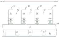
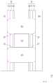
图1为本发明制作一动态随机存取存储器元件的上视图;1 is a top view of a dynamic random access memory device made by the present invention;
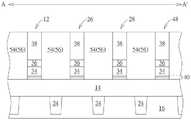
图2至图4为图1中沿着切线AA’方向制作动态随机存取存储器元件的方法示意图;2 to 4 are schematic diagrams of a method for fabricating a dynamic random access memory element along the tangent line AA' in FIG. 1;
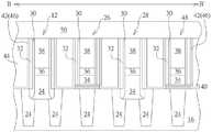
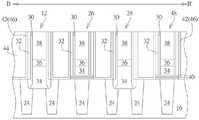
图5至图7为图1中沿着切线BB’方向制作动态随机存取存储器元件的方法示意图;5 to 7 are schematic diagrams of a method for fabricating a dynamic random access memory element along the tangent BB' direction in FIG. 1;
图8为图1中两相邻位线结构间的局部放大上视图。FIG. 8 is a partially enlarged top view between two adjacent bit line structures in FIG. 1 .
主要元件符号说明Description of main component symbols
10 动态随机存取存储器元件 12 位线结构10 DRAM element 12-bit line structure
14 字符线 16 基底14
18 主动区(有源区) 20 存储单元区18 Active area (active area) 20 Memory cell area
22 栅极 24 浅沟绝缘22 Gate 24 Shallow trench insulation
26 位线结构 28 位线结构26-bit line structure 28-bit line structure
30 第一间隙壁 32 第二间隙壁30
34 导电层 36 金属层34
38 掩模层 40 堆叠层38
42 衬垫层 44 层间介电层42
46 第三间隙壁 48 位线结构46 Third spacer 48-bit line structure
50 图案化掩模 52 开口50
54 介电层 56 存储节点接触隔离结构54
58 阻障层 60 导电层58
62 存储结点接触 64 间隙壁62
66 间隙壁 68 存储节点接触隔离结构66
具体实施方式Detailed ways
请参照图1至图8,图1至图8为本发明一实施例制作动态随机存取存储器元件的方法示意图,其中图1为本发明制作一DRAM动态随机存取存储器元件的上示图,图2至图4为图1中沿着切线AA’方向制作动态随机存取存储器元件的方法示意图,图5至图7为图1中沿着切线BB’方向制作动态随机存取存储器元件的方法示意图,图8则为图1中位于二相邻位线结构间的局部放大上视图。Please refer to FIGS. 1 to 8 . FIGS. 1 to 8 are schematic diagrams of a method for fabricating a dynamic random access memory device according to an embodiment of the present invention, wherein FIG. 1 is a top view of fabricating a DRAM dynamic random access memory device according to the present invention, 2 to 4 are schematic diagrams illustrating a method of fabricating a DRAM device along the tangent line AA' in FIG. 1 , and FIGS. 5 to 7 are diagrams illustrating a method of fabricating a DRAM device along the tangent BB' direction in FIG. 1 . FIG. 8 is a partial enlarged top view between two adjacent bit line structures in FIG. 1 .
本实施例是提供一存储器元件,例如是具备凹入式栅极的动态随机存取存储器元件10,其包含有至少一晶体管元件(图未示)以及至少一电容结构(图未示),以作为DRAM阵列中的最小组成单元并接收来自于位线或位线结构12、26、28、48及字符线14的电压信号。The present embodiment provides a memory element, such as a dynamic random
如图1所示,动态随机存取存储器元件10包含一基底16,例如一由硅所构成的半导体基底,然后于基底16内形成有至少一浅沟绝缘24,以于基底16上定义出多个主动区(active area,AA)18。此外,基底16上还定义有一存储单元区20以及一周边区(图未示)。其中,动态随机存取存储器元件10的多个字符线(word line,WL)14与多个位线(bit line,BL)结构12、26、28、48较佳形成于存储单元区20的基底16上而其他的主动元件等(未绘示)则可形成在周边区。需注意的是,为简化说明,本发明的图1仅绘示出位于存储单元区20的元件上视图并省略了位于周边区的元件。As shown in FIG. 1 , the dynamic random
在本实施例中,各主动区18例如是相互平行地朝向一第一方向延伸,而字符线14或多条栅极22是形成在基底16内并穿越各主动区18及浅沟绝缘24。具体来说,各栅极22是沿着不同于第一方向的一第二方向,例如Y方向延伸,且第二方向与第一方向相交并小于90度。In this embodiment, the
另一方面,位线结构12、26、28、48是相互平行地形成在基底16上沿着一第三方向,例如X方向延伸,并同样横跨各主动区18及浅沟绝缘24。其中,第三方向同样是不同于第一方向,并且较佳是与第二方向垂直。也就是说,第一方向、第二方向及第三方向彼此都不同,且第一方向与第二方向及第三方向都不垂直。此外,字符线14两侧的主动区18内较佳于后续制作工艺中形成接触插塞,例如包括位线接触插塞(bit line contact,BLC)(图未示)来电连接至各晶体管元件的源极/漏极区域(图未示)以及存储节点(storage node)接触插塞(图未示)来电连接一电容。On the other hand, the
以下针对形成字符线14(或又称埋入式字符线)后的制作进行说明。首先如图2及图5所示,先形成前述的位线或位线结构12、26、28、48于存储单元区20以及栅极结构(图未示)于周边区。在本实施例中,位线结构、12、26、28、48下方的基底16内可设有例如字符线14、浅沟隔离24以及主动区18,各位线结构12、26、28、48两侧分别设有第一间隙壁30以及第二间隙壁32,其中图5所示的位线结构12、28可包含一非金属导电层34、一选择性阻障层(图未示)、一金属层36以及一掩模层38,而位线结构26、48则包含一由氧化物-氮化物-氧化物所构成的堆叠层40、一非金属导电层34、一选择性阻障层(图未示)、一金属层36以及一掩模层38。在本实施例中,非金属导电层34可包括多晶硅、非晶硅或其他含硅或不含硅的非金属导电材料,阻障层可包括钛、钨硅化物(WSi)、氮化钨(WN)或其他适合的阻障材料,金属层36可包括铝、钨、铜、钛铝合金或其他适合的低电阻金属导电材料,而掩模层38可包括氮化硅、氮氧化硅、氮碳化硅(SiCN)或其他适合的绝缘材料。Hereinafter, the fabrication after forming the word line 14 (or also called a buried word line) will be described. First, as shown in FIGS. 2 and 5 , the aforementioned bit lines or
接着依序形成一衬垫层42以及一层间介电层44于存储单元区20的位线结构12、26、28、48、基底16以及浅沟隔离24上以及周边区的栅极结构上,其中衬垫层42于周边区可作为一接触洞蚀刻停止层而于存储单元区20则较佳成为一第三间隙壁46设于第二间隙壁32侧壁。在本实施例中,第一间隙壁30以及第三间隙壁46较佳包含相同材料而第二间隙壁32较佳与第一间隙壁30及第三间隙壁46由不同材料所构成,例如本实施例的第一间隙壁30及第三间隙壁46较佳由氮化硅或氮碳化硅所构成而第二间隙壁32则由氧化硅所构成。但不局限于此材料组合,依据本发明其他实施例第一间隙壁30以及第三间隙壁46可由第一种介电材料所构成而第二间隙壁32可由第二种介电材料所构成,同时三者均可选自由氧化硅、氮化硅、氮氧化硅以及氮碳化硅所构成的群组。层间介电层44较佳由氧化物,例如四乙氧基硅烷(Tetraethyl orthosilicate,TEOS)所构成,但不局限于此。Next, a
随后进行一平坦化制作工艺,例如利用化学机械研磨(chemical mechanicalpolishing,CMP)制作工艺去除部分衬垫层42以及部分层间介电层44,再形成一图案化掩模50于部分位线结构12、26、28、48上。值得注意的是,本阶段所形成的图案化掩模50较佳沿着Y方向覆盖两相邻字符线之间的位置(亦即图1中沿着切线BB’的方向),因此图5中沿着切线BB’的位线结构12、26、28、48以及层间介电层44上较佳设有图案化掩模50但图2沿着切线AA’的位线结构12、26、28、48以及层间介电层44上是裸露出来且无覆盖任何图案化掩模50。Then, a planarization process is performed, for example, a chemical mechanical polishing (CMP) process is used to remove part of the
随后如图3及图6所示,利用图案化掩模50进行一次或一次以上蚀刻制作工艺去除部分层间介电层44以及部分间隙壁并暴露出位线结构12、26、28、48侧壁,之后再去除图案化掩模50。更具体而言,本阶段所进行的蚀刻制作工艺较佳去除图2中沿着切线AA’方向所设置位线结构12、26、28、48间的所有层间介电层44与间隙壁包括第一间隙壁30、第二间隙壁32及第三间隙壁46,以于位线结构12、26、28、48间形成开口52并由此暴露出位线结构12、26、28、48侧壁。图6中沿着切线BB’方向所设置的位线结构12、26、28、48上方在蚀刻过程中由于有图案化掩模50遮蔽,因此在蚀刻制作工艺后位线结构12、26、28、48侧壁的第一间隙壁30、第二间隙壁32、第三间隙壁46以及层间介电层44仍存在。在本实施例中,蚀刻制作工艺所使用的蚀刻剂较佳选自由六氟丁二烯(C4F6)以及三氟甲烷(CHF3)所构成的群组,但不局限于此。Then, as shown in FIG. 3 and FIG. 6 , one or more etching processes are performed using the patterned
然后如图4所示,形成一介电层54于位线结构12、26、28、48间的开口52内并填满各开口52,接着再利用平坦化制作工艺,例如利用CMP去除部分介电层54使剩余的介电层54切齐位线结构12、26、28、48上表面,以于位线结构12、26、28、48间形成存储节点接触隔离结构(storage node contact isolation)56。在本实施例中,存储节点接触隔离结构56较佳包含氮碳化硅(SiCN)等介电材料,但不局限于此。Then, as shown in FIG. 4 , a
接着如图7所示,先利用光刻及蚀刻制作工艺去除图6沿着BB’方向所设置位线结构12、26、28、48间的部分层间介电层44以及部分第三间隙壁46,以于位线结构12、26、28、48间形成接触洞(图未示)。然后依序形成一选择性阻障层58以及一导电层60于接触洞内。之后再利用平坦化制作工艺例如CMP或另一道蚀刻制作工艺去除部分导电层60及部分阻障层58以形成存储结点接触62。在本实施例中,阻障层58可包含氮化钛、氮化钽或其组合,导电层60可包含铝、铬、铜、钽、钼、钨或其组合且最佳为钨。至此及完成本发明一实施例的动态随机存取存储器元件的制作。Next, as shown in FIG. 7 , a part of the
请继续参照图8,图8为图1中两相邻位线结构12、26间的局部放大上视图。如图8所示,本发明的半导体元件再经由上述制作工艺后主要包含二相邻位线结构例如位线结构12以及位线结构26沿着第一方向(例如X方向)延伸于基底16上,间隙壁64包含前述的第一间隙壁30、第二间隙壁32及第三间隙壁46沿着第一方向延伸于位线结构12,间隙壁66包含前述的第一间隙壁30、第二间隙壁32及第三间隙壁46沿着第一方向延伸于位线结构26旁,存储节点接触隔离结构56以及存储节点接触隔离结构68沿着第二方向(例如Y方向)延伸于位线结构12以及位线结构26之间,以及一存储节点接触62设于存储节点接触隔离结构56以及存储节点接触隔离结构68之间。Please continue to refer to FIG. 8 . FIG. 8 is a partially enlarged top view between two adjacent
其中存储节点接触隔离结构56直接接触位线结构12、设于位线结构12侧壁的间隙壁64、位线结构26、设于位线结构26侧壁的间隙壁66以及存储节点接触62。同样存储节点接触隔离结构68直接接触位线结构12、设于位线结构12侧壁的间隙壁64、位线结构26、设于位线结构26侧壁的间隙壁66以及存储节点接触62。另外设于中间的存储节点接触62则直接接触设于位线结构12侧壁的间隙壁64、设于位线结构26侧壁的间隙壁66、存储节点接触隔离结构56以及存储节点接触隔离结构68。从另一角度来看,各间隙壁64、66分别包含前述图3所形成的开口52暴露出部分位线结构12、26侧壁,而存储节点接触隔离结构56、68则经由开口52深入间隙壁64、66内直接接触位线结构12、26。The storage node
以上所述仅为本发明的优选实施例,凡依本发明权利要求所做的均等变化与修饰,都应属本发明的涵盖范围。The above descriptions are only preferred embodiments of the present invention, and all equivalent changes and modifications made according to the claims of the present invention shall fall within the scope of the present invention.
Claims (14)
Priority Applications (2)
| Application Number | Priority Date | Filing Date | Title |
|---|---|---|---|
| CN201810582040.XACN110581103B (en) | 2018-06-07 | 2018-06-07 | Semiconductor element and manufacturing method thereof |
| US16/026,069US10475794B1 (en) | 2018-06-07 | 2018-07-03 | Semiconductor device and method for fabricating the same |
Applications Claiming Priority (1)
| Application Number | Priority Date | Filing Date | Title |
|---|---|---|---|
| CN201810582040.XACN110581103B (en) | 2018-06-07 | 2018-06-07 | Semiconductor element and manufacturing method thereof |
Publications (2)
| Publication Number | Publication Date |
|---|---|
| CN110581103A CN110581103A (en) | 2019-12-17 |
| CN110581103Btrue CN110581103B (en) | 2022-04-12 |
Family
ID=68466455
Family Applications (1)
| Application Number | Title | Priority Date | Filing Date |
|---|---|---|---|
| CN201810582040.XAActiveCN110581103B (en) | 2018-06-07 | 2018-06-07 | Semiconductor element and manufacturing method thereof |
Country Status (2)
| Country | Link |
|---|---|
| US (1) | US10475794B1 (en) |
| CN (1) | CN110581103B (en) |
Families Citing this family (16)
| Publication number | Priority date | Publication date | Assignee | Title |
|---|---|---|---|---|
| US11329062B2 (en) | 2018-10-17 | 2022-05-10 | Micron Technology, Inc. | Memory arrays and methods used in forming a memory array |
| US11177278B2 (en) | 2019-11-06 | 2021-11-16 | Micron Technology, Inc. | Memory arrays and methods used in forming a memory array comprising strings of memory cells |
| US11121144B2 (en)* | 2019-11-13 | 2021-09-14 | Micron Technology, Inc. | Memory arrays and methods used in forming a memory array comprising strings of memory cells |
| US11177159B2 (en) | 2019-11-13 | 2021-11-16 | Micron Technology, Inc. | Memory arrays and methods used in forming a memory array comprising strings of memory cells |
| US11195560B2 (en)* | 2019-12-10 | 2021-12-07 | Micron Technology, Inc. | Integrated assemblies having void regions between digit lines and conductive structures, and methods of forming integrated assemblies |
| EP4163975A4 (en)* | 2020-07-16 | 2023-12-06 | Changxin Memory Technologies, Inc. | Semiconductor structure and manufacturing method therefor |
| CN114203702B (en)* | 2020-09-18 | 2025-01-14 | 长鑫存储技术有限公司 | Semiconductor structure and method for manufacturing the same |
| US12237215B2 (en) | 2020-09-18 | 2025-02-25 | Changxin Memory Technologies, Inc. | Semiconductor structure and method for manufacturing same |
| EP3998631B1 (en) | 2020-09-18 | 2024-01-24 | Changxin Memory Technologies, Inc. | Semiconductor structure and manufacturing method therefor |
| US11289492B1 (en)* | 2020-11-09 | 2022-03-29 | Nanya Technology Corporation | Semiconductor structure and method of manufacturing thereof |
| CN114695270B (en)* | 2020-12-30 | 2024-11-01 | 长鑫存储技术有限公司 | Method for manufacturing semiconductor device and semiconductor device |
| CN115084089B (en)* | 2021-03-16 | 2025-10-03 | 华邦电子股份有限公司 | Semiconductor structure and method for manufacturing the same |
| CN115513206B (en)* | 2021-06-23 | 2024-11-26 | 华邦电子股份有限公司 | Semiconductor memory structure and method for forming the same |
| US11910595B2 (en)* | 2021-07-06 | 2024-02-20 | Fujian Jinhua Integrated Circuit Co., Ltd. | Semiconductor memory device |
| US11991875B2 (en)* | 2021-09-01 | 2024-05-21 | Winbond Electronics Corp. | Semiconductor memory structure and the method for forming the same |
| CN113889474B (en)* | 2021-10-29 | 2025-10-03 | 福建省晋华集成电路有限公司 | Memory and manufacturing method thereof |
Citations (4)
| Publication number | Priority date | Publication date | Assignee | Title |
|---|---|---|---|---|
| CN101010799A (en)* | 2004-08-24 | 2007-08-01 | 微米技术有限公司 | Semiconductor construction with isolation regions for DRAM cell and production method |
| US9123550B2 (en)* | 2012-09-14 | 2015-09-01 | Samsung Electronics Co., Ltd. | Semiconductor devices using air spaces to separate conductive structures and methods of manufacturing the same |
| CN107240586A (en)* | 2017-07-26 | 2017-10-10 | 睿力集成电路有限公司 | Memory and forming method thereof, semiconductor devices |
| CN107342263A (en)* | 2017-07-07 | 2017-11-10 | 睿力集成电路有限公司 | Memory and forming method thereof, semiconductor devices |
Family Cites Families (5)
| Publication number | Priority date | Publication date | Assignee | Title |
|---|---|---|---|---|
| KR100587635B1 (en)* | 2003-06-10 | 2006-06-07 | 주식회사 하이닉스반도체 | Manufacturing Method of Semiconductor Device |
| JP2011243960A (en) | 2010-04-21 | 2011-12-01 | Elpida Memory Inc | Semiconductor device and manufacturing method thereof |
| KR20140016663A (en)* | 2012-07-30 | 2014-02-10 | 에스케이하이닉스 주식회사 | Semiconductor device and method for manufacturing the same |
| KR102004242B1 (en)* | 2013-12-13 | 2019-07-26 | 삼성전자주식회사 | Semiconductor device and method for fabricating the same |
| KR102255834B1 (en)* | 2015-03-20 | 2021-05-26 | 삼성전자주식회사 | Semiconductor device and method of fabricating the same |
- 2018
- 2018-06-07CNCN201810582040.XApatent/CN110581103B/enactiveActive
- 2018-07-03USUS16/026,069patent/US10475794B1/enactiveActive
Patent Citations (4)
| Publication number | Priority date | Publication date | Assignee | Title |
|---|---|---|---|---|
| CN101010799A (en)* | 2004-08-24 | 2007-08-01 | 微米技术有限公司 | Semiconductor construction with isolation regions for DRAM cell and production method |
| US9123550B2 (en)* | 2012-09-14 | 2015-09-01 | Samsung Electronics Co., Ltd. | Semiconductor devices using air spaces to separate conductive structures and methods of manufacturing the same |
| CN107342263A (en)* | 2017-07-07 | 2017-11-10 | 睿力集成电路有限公司 | Memory and forming method thereof, semiconductor devices |
| CN107240586A (en)* | 2017-07-26 | 2017-10-10 | 睿力集成电路有限公司 | Memory and forming method thereof, semiconductor devices |
Also Published As
| Publication number | Publication date |
|---|---|
| CN110581103A (en) | 2019-12-17 |
| US10475794B1 (en) | 2019-11-12 |
Similar Documents
| Publication | Publication Date | Title |
|---|---|---|
| CN110581103B (en) | Semiconductor element and manufacturing method thereof | |
| CN108389861B (en) | Semiconductor device and method for forming the same | |
| CN100561728C (en) | Semiconductor device and manufacturing method thereof | |
| CN108962825B (en) | Semiconductor element and manufacturing method thereof | |
| CN110061001B (en) | Semiconductor element and manufacturing method thereof | |
| CN100407425C (en) | Semiconductor device and manufacturing method thereof | |
| US7800155B2 (en) | Semiconductor device | |
| CN108511440B (en) | Semiconductor structure with capacitor connection pad and method of making capacitor connection pad | |
| JP4964407B2 (en) | Semiconductor device and manufacturing method thereof | |
| CN114068552B (en) | Semiconductor device and method for manufacturing the same | |
| US8148250B2 (en) | Method for manufacturing semiconductor device for preventing occurrence of short circuit between bit line contact plug and storage node contact plug | |
| CN116075153B (en) | Semiconductor structure and preparation method thereof | |
| KR101168606B1 (en) | wiring structure of semiconductor device and Method of forming a wiring structure | |
| CN108461449B (en) | Semiconductor element and manufacturing method thereof | |
| US11665888B2 (en) | Semiconductor device and method for fabricating the same | |
| CN114068428A (en) | Semiconductor memory device and method of forming the same | |
| CN101656254B (en) | Dynamic random access memory structure and manufacturing method thereof | |
| US20100148228A1 (en) | Semiconductor and manufacturing method of the same | |
| CN216563127U (en) | Semiconductor memory device with a plurality of memory cells | |
| CN113889474A (en) | Memory and manufacturing method thereof | |
| JP2009164534A (en) | Semiconductor device and manufacturing method therefor | |
| CN117529096B (en) | Method for manufacturing semiconductor device | |
| US20240032286A1 (en) | Integrated circuit devices | |
| KR20070019134A (en) | Semiconductor device and manufacturing method thereof | |
| KR100955263B1 (en) | Method of manufacturing semiconductor device |
Legal Events
| Date | Code | Title | Description |
|---|---|---|---|
| PB01 | Publication | ||
| PB01 | Publication | ||
| SE01 | Entry into force of request for substantive examination | ||
| SE01 | Entry into force of request for substantive examination | ||
| GR01 | Patent grant | ||
| GR01 | Patent grant |