CN110574234B - Antenna and MIMO antenna - Google Patents
Antenna and MIMO antennaDownload PDFInfo
- Publication number
- CN110574234B CN110574234BCN201880027795.1ACN201880027795ACN110574234BCN 110574234 BCN110574234 BCN 110574234BCN 201880027795 ACN201880027795 ACN 201880027795ACN 110574234 BCN110574234 BCN 110574234B
- Authority
- CN
- China
- Prior art keywords
- antenna
- resonator
- reflector
- waveguide
- ground plane
- Prior art date
- Legal status (The legal status is an assumption and is not a legal conclusion. Google has not performed a legal analysis and makes no representation as to the accuracy of the status listed.)
- Expired - Fee Related
Links
Images


Classifications
- H—ELECTRICITY
- H01—ELECTRIC ELEMENTS
- H01Q—ANTENNAS, i.e. RADIO AERIALS
- H01Q19/00—Combinations of primary active antenna elements and units with secondary devices, e.g. with quasi-optical devices, for giving the antenna a desired directional characteristic
- H01Q19/28—Combinations of primary active antenna elements and units with secondary devices, e.g. with quasi-optical devices, for giving the antenna a desired directional characteristic using a secondary device in the form of two or more substantially straight conductive elements
- H01Q19/30—Combinations of primary active antenna elements and units with secondary devices, e.g. with quasi-optical devices, for giving the antenna a desired directional characteristic using a secondary device in the form of two or more substantially straight conductive elements the primary active element being centre-fed and substantially straight, e.g. Yagi antenna
- H—ELECTRICITY
- H01—ELECTRIC ELEMENTS
- H01Q—ANTENNAS, i.e. RADIO AERIALS
- H01Q1/00—Details of, or arrangements associated with, antennas
- H01Q1/48—Earthing means; Earth screens; Counterpoises
- H—ELECTRICITY
- H01—ELECTRIC ELEMENTS
- H01Q—ANTENNAS, i.e. RADIO AERIALS
- H01Q1/00—Details of, or arrangements associated with, antennas
- H01Q1/52—Means for reducing coupling between antennas; Means for reducing coupling between an antenna and another structure
- H01Q1/521—Means for reducing coupling between antennas; Means for reducing coupling between an antenna and another structure reducing the coupling between adjacent antennas
- H01Q1/523—Means for reducing coupling between antennas; Means for reducing coupling between an antenna and another structure reducing the coupling between adjacent antennas between antennas of an array
- H—ELECTRICITY
- H01—ELECTRIC ELEMENTS
- H01Q—ANTENNAS, i.e. RADIO AERIALS
- H01Q19/00—Combinations of primary active antenna elements and units with secondary devices, e.g. with quasi-optical devices, for giving the antenna a desired directional characteristic
- H01Q19/10—Combinations of primary active antenna elements and units with secondary devices, e.g. with quasi-optical devices, for giving the antenna a desired directional characteristic using reflecting surfaces
- H—ELECTRICITY
- H01—ELECTRIC ELEMENTS
- H01Q—ANTENNAS, i.e. RADIO AERIALS
- H01Q21/00—Antenna arrays or systems
- H01Q21/0006—Particular feeding systems
- H—ELECTRICITY
- H01—ELECTRIC ELEMENTS
- H01Q—ANTENNAS, i.e. RADIO AERIALS
- H01Q21/00—Antenna arrays or systems
- H01Q21/06—Arrays of individually energised antenna units similarly polarised and spaced apart
- H01Q21/061—Two dimensional planar arrays
- H—ELECTRICITY
- H01—ELECTRIC ELEMENTS
- H01Q—ANTENNAS, i.e. RADIO AERIALS
- H01Q21/00—Antenna arrays or systems
- H01Q21/24—Combinations of antenna units polarised in different directions for transmitting or receiving circularly and elliptically polarised waves or waves linearly polarised in any direction
- H—ELECTRICITY
- H01—ELECTRIC ELEMENTS
- H01Q—ANTENNAS, i.e. RADIO AERIALS
- H01Q21/00—Antenna arrays or systems
- H01Q21/28—Combinations of substantially independent non-interacting antenna units or systems
- H—ELECTRICITY
- H01—ELECTRIC ELEMENTS
- H01Q—ANTENNAS, i.e. RADIO AERIALS
- H01Q5/00—Arrangements for simultaneous operation of antennas on two or more different wavebands, e.g. dual-band or multi-band arrangements
- H01Q5/40—Imbricated or interleaved structures; Combined or electromagnetically coupled arrangements, e.g. comprising two or more non-connected fed radiating elements
- H01Q5/48—Combinations of two or more dipole type antennas
- H01Q5/49—Combinations of two or more dipole type antennas with parasitic elements used for purposes other than for dual-band or multi-band, e.g. imbricated Yagi antennas
Landscapes
- Physics & Mathematics (AREA)
- Electromagnetism (AREA)
- Aerials With Secondary Devices (AREA)
- Variable-Direction Aerials And Aerial Arrays (AREA)
Abstract
Translated fromChinese
Description
Translated fromChinese技术领域technical field
本发明涉及一种天线和MIMO(Multiple Input and Multiple Output:多入多出)天线。The present invention relates to an antenna and a MIMO (Multiple Input and Multiple Output: Multiple Input and Multiple Output) antenna.
背景技术Background technique
以往,已知在与电路基板平行的方向上具有指向性的平面八木宇田天线(例如,参照专利文献1)。Conventionally, a planar Yagi-Uda antenna having directivity in a direction parallel to a circuit board has been known (for example, refer to Patent Document 1).
现有技术文献prior art literature
专利文献Patent Literature
专利文献1:日本特开2009-200719号公报Patent Document 1: Japanese Patent Laid-Open No. 2009-200719
发明内容SUMMARY OF THE INVENTION
发明要解决的问题Invention to solve problem
在专利文献1所记载的技术中,平衡系统的天线部分与非平衡系统的传输线路之间的连接需要平衡-不平衡变压器。然而,有时未必能够准备用于配置平衡-不平衡变压器的空间。In the technique described in
因而,本公开中提供一种即使不具有平衡-不平衡变压器也能够在特定的方向上得到指向性的天线。Therefore, the present disclosure provides an antenna capable of obtaining directivity in a specific direction without having a balun.
用于解决问题的方案solution to the problem
在本公开的一个方式中,提供一种天线,具备:接地平面;第一谐振器,其连接于以所述接地平面为基准的馈电点;第二谐振器,由所述第一谐振器通过电磁场耦合或磁场耦合来以非接触方式对该第二谐振器馈电;以及位于与所述第一谐振器及所述第二谐振器分离的位置的至少一个波导器,其中,所述天线将位于所述第二谐振器的与所述波导器相反的一侧的所述接地平面用作反射器,或者所述天线还具备位于所述第二谐振器的与所述波导器相反的一侧的反射器。In one aspect of the present disclosure, there is provided an antenna including: a ground plane; a first resonator connected to a feeding point with the ground plane as a reference; and a second resonator connected by the first resonator feeding the second resonator in a non-contact manner by electromagnetic field coupling or magnetic field coupling; and at least one waveguide at a location separate from the first resonator and the second resonator, wherein the antenna The ground plane on the opposite side of the second resonator from the waveguide is used as a reflector, or the antenna is further provided with a second resonator on the opposite side from the waveguide. side reflector.
发明的效果effect of invention
根据本公开,即使不具有平衡-不平衡变压器也能够在特定的方向上得到指向性。通过将本发明应用于便携式信息设备,能够实现设备的小型化,并且还能够实现天线的高性能化。因此,设备的设计的自由度提高,设计性也提高。According to the present disclosure, directivity can be obtained in a specific direction even without a balun. By applying the present invention to a portable information device, the miniaturization of the device can be achieved, and the performance of the antenna can also be increased. Therefore, the degree of freedom in the design of the device is improved, and the designability is also improved.
附图说明Description of drawings
图1是示意性地示出本公开所涉及的天线的结构的一例的平面图。FIG. 1 is a plan view schematically showing an example of a configuration of an antenna according to the present disclosure.
图2是示意性地示出本公开所涉及的天线的结构的一例的截面图。FIG. 2 is a cross-sectional view schematically showing an example of the structure of the antenna according to the present disclosure.
图3是示意性地示出本公开所涉及的天线的第一实施例的平面图。FIG. 3 is a plan view schematically showing a first embodiment of the antenna according to the present disclosure.
图4是示意性地示出本公开所涉及的天线的第一实施例的截面图。FIG. 4 is a cross-sectional view schematically showing a first embodiment of the antenna according to the present disclosure.
图5是示出对本公开所涉及的天线的第一实施例的回波损耗特性进行了分析的模拟的一例的图。FIG. 5 is a diagram showing an example of a simulation that analyzes the return loss characteristics of the first embodiment of the antenna according to the present disclosure.
图6是示出在本公开所涉及的天线的第一实施例中对水平极化波时的水平面内的指向性进行分析所得到的模拟结果的一例的图。6 is a diagram showing an example of a simulation result obtained by analyzing the directivity in the horizontal plane in the case of a horizontally polarized wave in the first embodiment of the antenna according to the present disclosure.
图7是示出在本公开所涉及的天线的第一实施例中对水平极化波时的垂直面内的指向性进行分析所得到的模拟结果的一例的图。7 is a diagram showing an example of a simulation result obtained by analyzing the directivity in the vertical plane in the case of a horizontally polarized wave in the first embodiment of the antenna according to the present disclosure.
图8是示意性地示出本公开所涉及的天线的第二实施例的平面图。FIG. 8 is a plan view schematically showing a second embodiment of the antenna according to the present disclosure.
图9是示出在本公开所涉及的天线的第二实施例中对天线之间的相关系数进行分析所得到的模拟结果的一例的图。9 is a diagram showing an example of a simulation result obtained by analyzing the correlation coefficient between the antennas in the second embodiment of the antenna according to the present disclosure.
图10是示出对本公开所涉及的天线的第二实施例的回波损耗特性进行了分析的模拟的一例的图。10 is a diagram showing an example of a simulation that analyzes the return loss characteristics of the second embodiment of the antenna according to the present disclosure.
图11是示出在本公开所涉及的天线的第二实施例中对水平极化波时的水平面内的指向性进行分析所得到的模拟结果的一例的图。11 is a diagram showing an example of a simulation result obtained by analyzing the directivity in the horizontal plane in the case of a horizontally polarized wave in the second embodiment of the antenna according to the present disclosure.
图12是示出在本公开所涉及的天线的第二实施例中对水平极化波时的垂直面内的指向性进行分析所得到的模拟结果的一例的图。12 is a diagram showing an example of a simulation result obtained by analyzing the directivity in the vertical plane in the case of a horizontally polarized wave in the second embodiment of the antenna according to the present disclosure.
图13是示意性地示出本公开所涉及的天线的第三实施例的立体图。FIG. 13 is a perspective view schematically showing a third embodiment of the antenna according to the present disclosure.
图14是示意性地示出本公开所涉及的天线的第三实施例的平面图。FIG. 14 is a plan view schematically showing a third embodiment of the antenna according to the present disclosure.
图15是示意性地示出本公开所涉及的天线的第三实施例的侧视图。FIG. 15 is a side view schematically showing a third embodiment of the antenna according to the present disclosure.
图16是示出对本公开所涉及的天线的第三实施例的回波损耗特性进行了分析的模拟的一例的图。16 is a diagram showing an example of a simulation that analyzes the return loss characteristics of the third embodiment of the antenna according to the present disclosure.
图17是示出在本公开所涉及的天线的第三实施例中对水平极化波时的水平面内的指向性进行分析所得到的模拟结果的一例的图。17 is a diagram showing an example of a simulation result obtained by analyzing the directivity in the horizontal plane in the case of a horizontally polarized wave in the third embodiment of the antenna according to the present disclosure.
图18是示出在本公开所涉及的天线的第三实施例中对水平极化波时的垂直面内的指向性进行分析所得到的模拟结果的一例的图。18 is a diagram showing an example of a simulation result obtained by analyzing the directivity in the vertical plane in the case of a horizontally polarized wave in the third embodiment of the antenna according to the present disclosure.
图19是示意性地示出本公开所涉及的天线的第四实施例的立体图。FIG. 19 is a perspective view schematically showing a fourth embodiment of the antenna according to the present disclosure.
图20是示意性地示出本公开所涉及的天线的第四实施例的平面图。FIG. 20 is a plan view schematically showing a fourth embodiment of the antenna according to the present disclosure.
图21是示出在本公开所涉及的天线的第四实施例中对天线之间的相关系数进行分析所得到的模拟结果的一例的图。21 is a diagram showing an example of a simulation result obtained by analyzing the correlation coefficient between the antennas in the fourth embodiment of the antenna according to the present disclosure.
图22是示出对本公开所涉及的天线的第四实施例的回波损耗特性进行了分析的模拟的一例的图。FIG. 22 is a diagram showing an example of a simulation that analyzes the return loss characteristics of the fourth embodiment of the antenna according to the present disclosure.
图23是示意性地示出本公开所涉及的天线的第五实施例的平面图。FIG. 23 is a plan view schematically showing a fifth embodiment of the antenna according to the present disclosure.
图24是示出在本公开所涉及的天线的第五实施例中对天线之间的相关系数进行分析所得到的模拟结果的一例的图。24 is a diagram showing an example of a simulation result obtained by analyzing the correlation coefficient between the antennas in the fifth embodiment of the antenna according to the present disclosure.
图25是示出对本公开所涉及的天线的第五实施例的回波损耗特性进行了分析的模拟的一例的图。FIG. 25 is a diagram showing an example of a simulation that analyzes the return loss characteristics of the fifth embodiment of the antenna according to the present disclosure.
图26是示意性地示出以由波导元件和辐射元件将导体夹在中间的方式将它们进行层叠的方式的图。FIG. 26 is a diagram schematically showing a manner of stacking a waveguide element and a radiating element so as to sandwich the conductors.
图27是说明能够通过对各元件的相对的位置关系进行调整来控制主波束的方向的图(其一)。FIG. 27 is a diagram (Part 1) explaining that the direction of the main beam can be controlled by adjusting the relative positional relationship of each element.
图28是说明能够通过对各元件的相对的位置关系进行调整来控制主波束的方向的图(其二)。FIG. 28 is a diagram (Part 2) explaining that the direction of the main beam can be controlled by adjusting the relative positional relationship of each element.
具体实施方式Detailed ways
下面,参照附图来说明本发明的实施方式。此外,在下面的说明中,X轴、Y轴、Z轴表示互相正交的轴,X轴方向、Y轴方向、Z轴方向分别表示与X轴、Y轴、Z轴平行的方向。Hereinafter, embodiments of the present invention will be described with reference to the accompanying drawings. In addition, in the following description, the X-axis, Y-axis, and Z-axis represent mutually orthogonal axes, and the X-axis direction, the Y-axis direction, and the Z-axis direction represent directions parallel to the X-axis, the Y-axis, and the Z-axis, respectively.
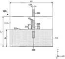
图1是示意性地示出本公开所涉及的天线的结构的一例的平面图。图2是示意性地示出本公开所涉及的天线的结构的一例的截面图。图1、图2所示的天线25被搭载于具备无线通信功能的电子设备。电子设备使用天线25来进行无线通信。作为搭载天线25的电子设备的具体例,能够例举无线终端装置(手机、智能电话、IoT(Internet of Things:物联网)设备等)、无线基站等。FIG. 1 is a plan view schematically showing an example of a configuration of an antenna according to the present disclosure. FIG. 2 is a cross-sectional view schematically showing an example of the structure of the antenna according to the present disclosure. The
天线25例如支持第五代移动通信系统(所谓的5G)、蓝牙(注册商标)等无线通信标准、IEEE802.11ac等无线LAN(Local Area Network:局域网)标准。天线25例如形成为能够接收发送频率为3GHz~30GHz的SHF(Super High Frequency:超高频)频带的电波、频率为30GHz~300GHz的EHF(Extremely High Frequency:极高频)频带的电波。天线25连接于利用接地件14的非平衡的传输线路的终端12。The
作为传输线路的具体例,能够例举微带线、带线、带接地平面的共面波导(在与形成信号线的导体面相反一侧的表面配置有接地平面的共面波导)、共面带线等。Specific examples of the transmission line include a microstrip line, a strip line, a coplanar waveguide with a ground plane (a coplanar waveguide in which a ground plane is arranged on the surface opposite to the conductor plane forming the signal line), a coplanar wave line, etc.
天线25具备接地件14、馈电元件21以及辐射元件22。The
接地件14是接地平面的一例。接地件外缘14a沿X轴方向延伸,是接地件14的直线的外缘的一例。接地件14被配置成与包括X轴和Y轴的XY平面平行,例如是形成于与XY平面平行的基板13上的接地图案。The
基板13是以电介质为主成份的部件。作为基板13的具体例,能够例举FR4(FlameRetardant Type4:耐燃类型4)基板。基板13可以是具有挠性的挠性基板。基板13具有第一基板表面以及位于与第一基板表面相反的一侧的第二基板表面。例如,在第一基板表面上安装电子电路,在第二基板表面上形成接地件14。此外,接地件14既可以形成在第一基板表面,也可以形成在基板13的内部。The
安装于基板13的电子电路例如是包括经由天线25接收信号的接收功能以及经由天线25发送信号的发送功能中的至少一个功能的集成电路。电子电路例如是由IC(Integrated Circuit)芯片实现的。包括接收功能和发送功能中的至少一个功能的集成电路还被称作通信用IC。The electronic circuit mounted on the
馈电元件21是连接于以接地平面为基准的馈电点的第一谐振器的一例。馈电元件21连接于传输线路的终端12。终端12是以接地件14为接地基准的馈电点的一例。The feeding
馈电元件21既可以配置于基板13,也可以配置于基板13以外的部位。在馈电元件21配置于基板13的情况下,馈电元件21例如是形成于基板13的第一基板表面上的导体图案。The feeding
馈电元件21向远离接地件14的方向延伸,且被连接于以接地件14为接地基准的馈电点(终端12)。馈电元件21是能够以非接触方式与辐射元件22高频耦合来对辐射元件22馈电的线状导体。附图中例示了如下的馈电元件21:该馈电元件21由沿着与接地件外缘14a成直角的方向延伸的直线状导体以及与接地件外缘14a并行地延伸的直线状导体形成为L字形。在图示的情况下,馈电元件21以终端12为起点从端部21a延伸,在弯曲部21c处弯曲,并延伸至顶端部21b。顶端部21b是没有连接其它导体的开放端。馈电元件21具备具有与X轴平行的方向分量的导体部分。在附图中例示了L字形的馈电元件21,但是馈电元件21的形状也可以是直线状、蜿蜒状、环状等其它形状。The feeding
辐射元件22是与第一谐振器接近的第二谐振器的一例。辐射元件22例如以与馈电元件21分离的方式配置,通过馈电元件21进行谐振来作为辐射导体发挥功能。辐射元件22例如通过与馈电元件21电磁场耦合或磁场耦合而以非接触方式被馈电,从而作为辐射导体发挥功能。电磁场耦合是指通过电磁波实现的非接触耦合。磁场耦合是指通过电磁耦合或电磁感应实现的非接触耦合。The
即,在本发明中,非接触耦合中的静电电容耦合(也简称为静电耦合或电容耦合)被排除。这是因为,与当平板电容器之间的距离变动时静电电容值变动的情况同样地,当在两个导体之间发生静电电容耦合时,两个导体之间形成的静电电容的值会因距离的变动而变动,谐振频率也因静电电容的值的变动而变动。反过来讲,如果进行电磁场耦合,则因距离的变动产生的谐振频率的变化能够抑制为优选10%以内,更优选为5%以内,进一步优选为3%以内。That is, in the present invention, electrostatic capacitive coupling (also simply referred to as electrostatic coupling or capacitive coupling) in non-contact coupling is excluded. This is because, as in the case where the capacitance value fluctuates when the distance between the plate capacitors fluctuates, when capacitive coupling occurs between two conductors, the value of the electrostatic capacitance formed between the two conductors varies depending on the distance. fluctuates, and the resonant frequency also fluctuates due to fluctuations in the value of the electrostatic capacitance. Conversely, if electromagnetic field coupling is performed, the variation of the resonance frequency due to the variation of the distance can be suppressed to preferably within 10%, more preferably within 5%, and still more preferably within 3%.
另外,当在两个导体之间发生静电电容耦合时,在两个导体之间流过位移电流(与在平板电容器之间流过位移电流的情况相同),这是因为两个导体不是作为独立的谐振器发挥作用,而是成为一体地作为一个谐振器发挥作用。In addition, when electrostatic capacitive coupling occurs between the two conductors, a displacement current flows between the two conductors (the same as the case where the displacement current flows between the plate capacitors), because the two conductors are not as independent function as a resonator, but as one resonator.
此外,将静电电容耦合排除意味着静电电容耦合没有以支配实质上的耦合的方式存在,具体来讲,意味着只要两个导体分别作为独立的谐振器工作,就能够无视静电电容耦合。Furthermore, the exclusion of electrostatic capacitive coupling means that electrostatic capacitive coupling does not exist so as to dominate substantial coupling. Specifically, it means that electrostatic capacitive coupling can be ignored as long as each of the two conductors operates as an independent resonator.
辐射元件22具备具有与X轴平行的方向分量的导体部分。例如,辐射元件22具有以沿着与X轴方向平行的接地件外缘14a的方式延伸的导体部分41。导体部分41位于与接地件外缘14a分离的位置。辐射元件22具有沿着接地件外缘14a的导体部分41,由此例如能够容易地调整天线25的指向性。The radiating
馈电元件21和辐射元件22例如以相隔彼此能够电磁场耦合的距离的方式配置。辐射元件22具有用于从馈电元件21接受馈电的馈电部。在附图中,作为馈电部,示出导体部分41。由馈电部经由馈电元件21通过电磁场耦合来以非接触方式对辐射元件22馈电。通过被这样馈电,辐射元件22作为天线25的辐射导体发挥功能。The feeding
由馈电元件21通过电磁场耦合来以非接触方式对辐射元件22馈电,由此在辐射元件22上流过与半波长偶极天线的谐振电流同样的谐振电流(在一个顶端部23与另一个顶端部24之间以驻波状分布的电流)。即,由馈电元件21通过电磁场耦合来以非接触方式对辐射元件22馈电,由此辐射元件22作为偶极天线发挥功能。The radiating
因而,由馈电元件21通过电磁场耦合来以非接触方式对辐射元件22馈电,因此即使不具有平衡-不平衡变压器,也能够将天线25连接于非平衡的传输线路。此外,在由馈电元件21通过磁场耦合来以非接触方式对辐射元件22馈电的方式中也同样地,即使不具有平衡-不平衡变压器,也能够将天线25连接于非平衡的传输线路。另外,当天线的动作频率被高频化为6GHz以上时,为了降低通信用IC与天线之间的传输损失,考虑将天线和通信用IC配置在同一基板上。在这样的情况下,需要考虑到来自通信用IC的发热来选定天线基板材料,但在本技术中,能够将通信用IC与天线以在物理上分离的方式连接,因此能够防止向天线传导热,从而能够增加天线基板(例如基材部30)的选择项。例如,能够将耐热性低的树脂等用作天线基板材料。Therefore, since the radiating
辐射元件22设置于电性的基材部30。基材部30例如是具有平面部的基板。辐射元件22的一部分或全部既可以设置在基材部30的表面,也可以设置在基材部30的内部。在图示的方式中,辐射元件22配置在基材部30的内侧表面(与接地件14相向的表面)。另外,基材部30优选为低介电损耗材料。通过设为这种结构,能够使天线性能提高。另外,由于不需要在基板13上形成天线,因此基板13能够利用FR4等通用基板材料。The
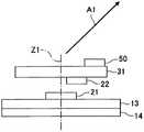
天线25具有包括由辐射元件22、波导器50、反射器60构成的平面八木宇田天线的结构。辐射元件22作为辐射器(radiator)发挥功能。波导器50和反射器60是以与馈电元件21及辐射元件22分离的方式配置的导体构件。The
天线25具备位于辐射元件22的特定的方向(在图示的方式中,是与接地件14平行的Y轴方向上的正侧)的至少一个波导器50。波导器50具备具有与X轴平行的方向分量的导体部分。附图中示出两个波导器51、52。波导器51、52各自的长度比辐射元件22的长度短。波导器也称为波导元件。The
即,将辐射元件22、波导元件51、52的长度分别设为L22、L51、L52。L51优选为L22的0.8~0.99倍,更优选为0.85~0.95倍。同样地,L52优选为比L51短,更优选为L51的0.8~0.99倍,进一步优选为0.85~0.95倍。图中是波导元件为两个的情况的例子,但也可以是三个以上,在该情况下,优选维持L51与L52之间的上述那样的关系,并且随着从Y轴方向上的负侧去向Y轴方向上的正侧使各个波导元件的长度递减。That is, let the lengths of the
另外,优选将辐射元件22和波导元件51、52配置为平行或者大致平行,关于它们之间的间隔(两个元件之间的最短的距离)d1、d2,当将谐振时的波长设为λ时,优选间隔d1、d2均为0.2λ~0.3λ,更优选为0.23λ~0.27λ。In addition, it is preferable to arrange the
波导器51、52被设置于基材部30,在图示的方式中,被配置于基材部30的内侧表面。另外,在图示的方式中,波导器51、52与辐射元件22被配置于同一表面。The
天线25具备位于辐射元件22的与波导器50相反的一侧的一个反射器60。反射器60具备具有与X轴平行的方向分量的导体部分。在图示的方式中,反射器60位于辐射元件22及馈电元件21的与波导器50相反的一侧。由于反射器60位于辐射元件22及馈电元件21双方的与波导器50相反的一侧,因此相比于反射器60位于馈电元件21的辐射元件22侧的方式而言,能够使天线25小型化。反射器也称为反射元件。The
反射器60的长度比辐射元件22的长度长。当将反射器60的长度设为L60时,L60优选为L22的1.01~1.2倍,更优选为1.05~1.15倍。另外,优选将反射器60与辐射元件22配置为平行或者大致平行,关于它们之间的间隔(两个元件之间的最短的距离)d3,当将谐振时的波长设为λ时,优选均为0.2λ~0.3λ,更优选设为0.23λ~0.27λ。The length of the
反射器60被设置于基材部30,在图示的方式中,被配置于基材部30的内侧表面。另外,在图示的方式中,反射器60以与接地件14相向的方式与辐射元件22配置于同一表面。反射器60与接地件14相向地配置。由此,相比于反射器60被配置于不与接地件14相向的部位的方式(例如,反射器60位于接地件外缘14a的辐射元件22侧的方式)而言,能够使天线25小型化。The
这样,天线25具备位于辐射元件22的特定的方向(在图示的方式中,是与接地件14平行的Y轴方向上的正侧)的至少一个波导器50以及位于辐射元件22的与波导器50相反的一侧的一个反射器60。由此,能够实现在辐射元件22的特定的方向上(在图示的方式中,是与接地件14平行的Y轴方向上的正侧)具有指向性的天线25。特别是,辐射元件22、波导器50以及反射器60分别具备具有与接地件14平行的方向分量的导体部分。因而,能够在辐射元件22的特定的方向上(在图示的方式中,是与接地件14平行的Y轴方向上的正侧)提高水平极化波的天线增益。In this way, the
在图1、图2中,天线25具备位于辐射元件22的与波导器50相反的一侧的反射器60。然而,天线25也可以将位于辐射元件22的与波导器50相反的一侧的接地件14用作反射器。在将接地件14用作反射器的情况下,也可以不具有图示的反射器60。在该情况下,也能够实现在辐射元件22的特定的方向上(在图示的方式中,是与接地件14平行的Y轴方向上的正侧)具有指向性的天线25。另外,辐射元件22和波导器50也可以与馈电元件21处于同一平面上。In FIGS. 1 and 2 , the
作为其它方式,也可以是,将波导元件50和辐射元件22以将导体31(例如便携设备的壳体等)夹在中间的方式层叠。图26中示出概要图。在图26中,使波导器50和辐射元件22层叠在导体31的两个面。此外,图26示出波导元件50为一个的例子,但是波导元件50的个数也可以是两个以上的多个。在该情况下,优选使电介质介于波导元件之间。在波导元件为多个的情况下,在将谐振时的波长设为λ时,波导元件的间隔优选设为0.2λ~0.3λ,更优选设为0.23λ~0.27λ。另外,优选波导元件、反射元件以及辐射元件的长度的关系也设为与图1同样。Alternatively, the
另外,如图27所示,在将波导元件50、辐射元件22以及反射元件(或接地件14)以平行或者大致平行的方式进行了层叠的状态下,调整各元件的相对的位置关系,由此能够控制指向性。例如,如图27那样,当使各元件的中心在与各元件中的一个元件的长边方向垂直的方向Z1上呈直线状地对齐时,主要的辐射方向A1为该垂直的方向Z1。另一方面,如图28那样,通过使各元件的中心逐渐地远离与各元件中的一个元件的长边方向垂直的方向Z1,能够使主要的辐射方向A1向逐渐地远离的该方向倾斜。通过将具有图27的结构的天线和具有图28的结构的天线一起使用,能够疑似地形成向全方位的方向辐射的天线。In addition, as shown in FIG. 27 , in a state where the
<第一实施例><First Embodiment>
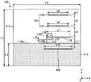
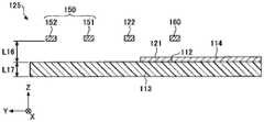
图3是示意性地示出本公开所涉及的天线的第一实施例的平面图。图4是示意性地示出本公开所涉及的天线的第一实施例的截面图。关于第一实施例的结构中的与上述的结构同样的结构,通过引用上述的说明来省略或简化说明。FIG. 3 is a plan view schematically showing a first embodiment of the antenna according to the present disclosure. FIG. 4 is a cross-sectional view schematically showing a first embodiment of the antenna according to the present disclosure. About the same structure as the above-mentioned structure among the structures of the first embodiment, the description is omitted or simplified by citing the above-mentioned description.
在图3、图4中,天线125是天线25(参照图1)的一例。天线125具备接地件114、馈电元件121、辐射元件122、波导器150以及反射器160。In FIGS. 3 and 4 , the
接地件114是接地件14(参照图1)的一例。接地件外缘114a是接地件114的直线的外缘的一例。接地件114例如是形成于与XY平面平行的基板113上的接地图案。基板113是基板13(参照图1)的一例。馈电元件121是馈电元件21(参照图1)的一例。馈电元件121连接于传输线路的终端112。终端112是以接地件114为接地基准的馈电点的一例。辐射元件122是辐射元件22(参照图1)的一例。辐射元件122通过与馈电元件121电磁场耦合而以非接触方式被馈电,从而作为辐射导体发挥功能。波导器150是波导器50(参照图1)的一例。在附图中示出两个波导器151、152。反射器160是反射器60(参照图1)的一例。The grounding
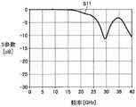
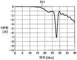
图5是示出对天线125的回波损耗特性进行了分析的模拟的一例的图。作为电磁场模拟,使用Microwave Studio(注册商标)(CST公司)。纵轴表示S参数(Scatteringparameters:散射参数)的反射系数S11。FIG. 5 is a diagram showing an example of a simulation in which the return loss characteristic of the
S11为极小值时的频率是能够取得阻抗匹配的频率,能够将该频率设为天线125的动作频率(谐振频率)。如图5所示,根据天线125,在包含28GHz的频带处能够得到良好的阻抗匹配。The frequency at which S11 is a minimum value is a frequency at which impedance matching can be achieved, and this frequency can be set as the operating frequency (resonance frequency) of the
图6是示出在天线125中对水平极化波时的水平面内的指向性进行分析所得到的模拟结果的一例的图。图7是示出在天线125中对水平极化波时的垂直面内的指向性进行分析所得到的模拟结果的一例的图。图6、图7示出天线125的基本模式的谐振频率f(=28GHz)处的指向性增益。FIG. 6 is a diagram showing an example of a simulation result obtained by analyzing the directivity in the horizontal plane in the case of a horizontally polarized wave in the
在图6、图7的分析时,将天线125的辐射元件122的一个顶端部(馈电元件121接近的一侧的顶端部)设为X轴、Y轴以及Z轴相交的原点。φ(Phi)表示包括X轴和Y轴的平面内的任意的方向与X轴所成的角度,θ(Theta)表示包括φ所指的方向和Z轴的平面内的任意的方向与Z轴所成的角度。In the analysis of FIGS. 6 and 7 , one tip of the radiating
如图6、图7所示,能够实现在辐射元件122的Y轴方向上的正侧具有指向性的天线125。因而,通过以使接地件114与水平面平行的方式配置天线125,来在与水平面平行的方向(水平方向)上提高Y轴方向上的正侧的指向性。因而,能够使从Y轴方向上的正侧到来的或者向Y轴方向上的正侧辐射的水平极化波的天线增益(动作增益)增大。As shown in FIGS. 6 and 7 , the
此外,在图5~图7中对S参数和天线增益进行分析时,当将单位设为mm时,图3、图4所示的各部分的尺寸如下:In addition, when the S-parameters and antenna gain are analyzed in Figures 5 to 7, when the unit is set to mm, the dimensions of each part shown in Figures 3 and 4 are as follows:
L1:10L1: 10
L2:4L2: 4
L3:12L3: 12
L4:3.6L4: 3.6
L5:0.12L5: 0.12
L6:3.8L6: 3.8
L7:4.2L7: 4.2
L8:1.88L8: 1.88
L9:1.88L9: 1.88
L10:5L10: 5
L11:1.88L11: 1.88
L12:0.94L12: 0.94
L13:1.06L13: 1.06
L14:0.56L14: 0.56
L15:0.12L15: 0.12
L16:0.25L16: 0.25
L17:0.05。L17: 0.05.
另外,天线125的各导体在Z轴方向上的厚度为0.018μm。另外,在馈电点(终端112)没有连接平衡-不平衡变压器。In addition, the thickness of each conductor of the
<第二实施例><Second Embodiment>
图8是示意性地示出本公开所涉及的天线的第二实施例的平面图。关于第二实施例的结构中的与上述的结构同样的结构,通过引用上述的说明来省略或简化说明。FIG. 8 is a plan view schematically showing a second embodiment of the antenna according to the present disclosure. Regarding the configuration of the second embodiment that is the same as the configuration described above, the description is omitted or simplified by citing the above description.
在图8中,天线225是具备馈电点互不相同的多个天线的MIMO(Multiple Inputand Multiple Output:多入多出)天线的一例。天线225具有两个天线125A、125B。天线125A、125B分别具有与天线125相同的结构(参照图3、图4)。天线125A、125B以沿X轴方向排列的方式配置,且共用接地件114。In FIG. 8 , the
图9是示出在天线225中对天线125A与天线125B之间的相关系数进行分析所得到的模拟结果的一例的图。如图9所示,相关系数在天线125A和天线125B各自的包含谐振频率f(=28GHz)的频带处为规定值(例如0.3)以下的低的状态。因而,能够使天线225作为水平极化波用的MIMO天线发挥功能。FIG. 9 is a diagram showing an example of a simulation result obtained by analyzing the correlation coefficient between the
图10是示出对天线225的回波损耗特性进行了分析的模拟的一例的图。作为电磁场模拟,使用Microwave Studio(注册商标)(CST公司)。纵轴表示S参数(Scatteringparameters)的反射系数S11和传递系数S12。FIG. 10 is a diagram showing an example of a simulation in which the return loss characteristic of the
反射系数S11为极小值时的频率是能够取得阻抗匹配的频率,能够将该频率设为天线125的动作频率(谐振频率)。另外,传递系数S12为极小值时的频率是能够提高天线之间的隔离度的频率(换言之,是能够使天线之间的相关系数低的频率)。The frequency at which the reflection coefficient S11 is a minimum value is a frequency at which impedance matching can be achieved, and this frequency can be set as the operating frequency (resonance frequency) of the
在图10中,反射系数S11表示天线125A的反射特性,传递系数S12表示从天线125B向天线125A的传递系数。如图10所示,在天线225的包含谐振频率28GHz的频带(例如25GHz~30GHz)处,反射系数S11和传递系数S12被抑制得低。因而,能够使天线225作为在谐振频率28GHz时使天线125A与天线125B之间的隔离度高的MIMO天线发挥功能。In FIG. 10 , the reflection coefficient S11 represents the reflection characteristic of the
图11是示出在天线225中对水平极化波时的水平面内的指向性进行分析所得到的模拟结果的一例的图。图12是示出在天线225中对水平极化波时的垂直面内的指向性进行分析所得到的模拟结果的一例的图。图11、图12示出天线225的基本模式的谐振频率f(=28GHz)处的指向性增益。FIG. 11 is a diagram showing an example of a simulation result obtained by analyzing the directivity in the horizontal plane in the case of a horizontally polarized wave in the
在图11、图12的分析时,将天线125A的辐射元件122的一个顶端部与天线125B的辐射元件122的一个顶端部的中点设为X轴、Y轴以及Z轴相交的原点。两个天线各自的一个顶端部表示馈电元件121接近的一侧的顶端部。φ(Phi)表示包括X轴和Y轴的平面内的任意的方向与X轴所成的角度,θ(Theta)表示包括φ所指的方向和Z轴的平面内的任意的方向与Z轴所成的角度。In the analysis of FIGS. 11 and 12 , the midpoint of one tip of the radiating
如图11、图12所示,能够实现在两个辐射元件122的Y轴方向上的正侧具有指向性的天线225。因而,通过以使接地件114与水平面平行的方式配置天线225,来在与水平面平行的方向(水平方向)上提高Y轴方向上的正侧的指向性。由此,能够使从Y轴方向上的正侧到来的或者向Y轴方向上的正侧辐射的水平极化波的天线增益(动作增益)增大。As shown in FIGS. 11 and 12 , the
此外,在图9~图12中对S参数和天线增益进行分析时,当将单位设为mm时,图8所示的各部分的尺寸如下:In addition, when the S-parameter and the antenna gain are analyzed in FIGS. 9 to 12, when the unit is mm, the dimensions of each part shown in FIG. 8 are as follows:
L1:10L1: 10
L2:4L2: 4
L3:12L3: 12
L20:5.2L20: 5.2
L21:1.08。L21: 1.08.
除此以外的尺寸与第一实施例相同。另外,在两个馈电点(终端112)没有连接平衡-不平衡变压器。Dimensions other than this are the same as in the first embodiment. In addition, no balun is connected at the two feed points (terminal 112).
<第三实施例><Third Embodiment>
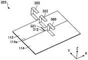
图13是示意性地示出本公开所涉及的天线的第三实施例的立体图。图14是示意性地示出本公开所涉及的天线的第三实施例的平面图。图15是示意性地示出本公开所涉及的天线的第三实施例的侧视图。关于第三实施例的结构中的与上述的结构同样的结构,通过引用上述的说明来省略或简化说明。FIG. 13 is a perspective view schematically showing a third embodiment of the antenna according to the present disclosure. FIG. 14 is a plan view schematically showing a third embodiment of the antenna according to the present disclosure. FIG. 15 is a side view schematically showing a third embodiment of the antenna according to the present disclosure. Regarding the configuration of the third embodiment that is the same as the above-described configuration, the description is omitted or simplified by citing the above-described description.
在图13~图15中,天线325是天线25(参照图1)的一例。天线325具备接地件114、馈电元件321、辐射元件322、波导器350以及反射器360。In FIGS. 13 to 15 , the
接地件114是接地件14(参照图1)的一例。接地件外缘114a是接地件114的直线的外缘的一例。接地件114例如是形成于与XY平面平行的基板113上的接地图案。基板113是基板13(参照图1)的一例。馈电元件321是馈电元件21(参照图1)的一例。馈电元件321连接于传输线路的终端312。终端312是以接地件114为接地基准的馈电点的一例。辐射元件322是辐射元件22(参照图1)的一例。辐射元件322通过与馈电元件321电磁场耦合而以非接触方式被馈电,从而作为辐射导体发挥功能。波导器350是波导器50(参照图1)的一例。附图中示出一个波导器350。反射器360是反射器60(参照图1)的一例。The grounding
在天线325中,辐射元件322、波导器350以及反射器360分别具备具有与接地件114的法线方向平行的方向分量的导体部分322b、360b、350b。由此,能够在辐射元件22的特定的方向上(在图示的方式中,是与接地件114平行的Y轴方向上的正侧)提高垂直极化波的天线增益。In the
在图示的方式中,辐射元件322、波导器350以及反射器360分别是U字形(包括J字形)的导体。各个U字形的开口部朝向Y轴方向上的负侧开口,具体来讲,朝向辐射元件322的配置有反射器360的一侧开口。In the illustrated manner, the
辐射元件322具有沿Z轴方向相向的一对导体部分322a、322c、以及将一对导体部分322a、322c各自的Y轴方向上的正侧的端部进行连接的导体部分322b。一对导体部分322a、322c沿Y轴方向延伸,导体部分322b沿Z轴方向延伸。The
波导器350具有沿Z轴方向相向的一对导体部分350a、350c、以及将一对导体部分350a、350c各自的Y轴方向上的正侧的端部进行连接的导体部分350b。一对导体部分350a、350c沿Y轴方向延伸,导体部分350b沿Z轴方向延伸。The
反射器360具有沿Z轴方向相向的一对导体部分360a、360c、以及将一对导体部分360a、360c各自的Y轴方向上的正侧的端部进行连接的导体部分360b。一对导体部分360a、360c沿Y轴方向延伸,导体部分360b沿Z轴方向延伸。The
在图13~图15中,天线325具备位于辐射元件322的与波导器350相反的一侧的反射器360。然而,天线325也可以将位于辐射元件322的与波导器350相反的一侧的接地件114用作反射器。在将接地件114用作反射器的情况下,也可以不具有图示的反射器360。在该情况下,也能够实现在辐射元件322的特定的方向上(在图示的方式中,是与接地件14平行的Y轴方向上的正侧)具有指向性的天线325。In FIGS. 13 to 15 , the
图16是示出对天线325的回波损耗特性进行了分析的模拟的一例的图。作为电磁场模拟,使用Microwave Studio(注册商标)(CST公司)。纵轴表示S参数(Scatteringparameters)的反射系数S11。FIG. 16 is a diagram showing an example of a simulation in which the return loss characteristic of the
S11为极小值时的频率是能够取得阻抗匹配的频率,能够将该频率设为天线325的动作频率(谐振频率)。如图16所示,根据天线325,在包含28GHz的频带处能够得到良好的阻抗匹配。The frequency at which S11 is a minimum value is a frequency at which impedance matching can be achieved, and this frequency can be set as the operating frequency (resonance frequency) of the
图17是示出在天线325中对垂直极化波时的垂直面内的指向性进行分析所得到的模拟结果的一例的图。图18是示出在天线325中对垂直极化波时的水平面内的指向性进行分析所得到的模拟结果的一例的图。图17、图18表示天线325的基本模式的谐振频率f(=28GHz)处的指向性增益。FIG. 17 is a diagram showing an example of a simulation result obtained by analyzing the directivity in the vertical plane in the case of vertically polarized waves in the
在图17、图18的分析时,将包括辐射元件322、波导器350以及反射器360的YZ平面与接地件外缘114a的交点设为X轴、Y轴以及Z轴相交的原点。φ(Phi)表示包括X轴和Y轴的平面内的任意的方向与X轴所成的角度,θ(Theta)表示包括φ所指的方向和Z轴的平面内的任意的方向与Z轴所成的角度。17 and 18, the intersection of the YZ plane including the
如图17、图18所示,能够实现在辐射元件322的Y轴方向上的正侧具有指向性的天线325。因而,通过以使接地件114与水平面平行的方式配置天线325,来在与水平面平行的方向(水平方向)上提高Y轴方向上的正侧的指向性。由此,能够使从Y轴方向上的正侧到来的或者向Y轴方向上的正侧辐射垂直极化波的天线增益(动作增益)增大。As shown in FIGS. 17 and 18 , the
此外,在图16~图18中对S参数和天线增益进行分析时,当将单位设为mm时,图14、图15所示的各部分的尺寸如下:In addition, when the S-parameter and the antenna gain are analyzed in FIGS. 16 to 18, when the unit is mm, the dimensions of each part shown in FIGS. 14 and 15 are as follows:
L1:10L1: 10
L2:4L2: 4
L3:12L3: 12
L30:0.5L30: 0.5
L31:0.12L31: 0.12
L32:1L32: 1
L33:1.61L33: 1.61
L34:0.89L34: 0.89
L35:1.61L35: 1.61
L36:0.89L36: 0.89
L37:1.61L37: 1.61
L38:1.62L38: 1.62
L39:0.191。L39: 0.191.
除此以外的尺寸与第一实施例相同。另外,在馈电点(终端312)没有连接平衡-不平衡变压器。Dimensions other than this are the same as in the first embodiment. Additionally, no balun is connected at the feed point (terminal 312).
<第四实施例><Fourth Embodiment>
图19是示意性地示出本公开所涉及的天线的第四实施例的立体图。图20是示意性地示出本公开所涉及的天线的第四实施例的平面图。关于第四实施例的结构中的与上述的结构同样的结构,通过引用上述的说明来省略或简化说明。FIG. 19 is a perspective view schematically showing a fourth embodiment of the antenna according to the present disclosure. FIG. 20 is a plan view schematically showing a fourth embodiment of the antenna according to the present disclosure. Regarding the configuration of the fourth embodiment that is the same as the above-described configuration, the description is omitted or simplified by citing the above-described description.
在图19、图20中,天线425是具备馈电点互不相同的多个天线的MIMO天线的一例。天线425具有两个天线325A、325B。天线325A、325B分别具有与天线325相同的结构(参照图13~图15)。天线325A、325B以沿X轴方向排列的方式配置,且共用接地件114。In FIGS. 19 and 20 , the
图21是示出在天线425中对天线325A与天线325B之间的相关系数进行分析所得到的模拟结果的一例的图。如图21所示,相关系数在天线325A和天线325B各自的包含谐振频率f(=28GHz)频带处为规定值(例如0.3)以下的低的状态。因而,能够使天线425作为垂直极化波用的MIMO天线发挥功能。FIG. 21 is a diagram showing an example of a simulation result obtained by analyzing the correlation coefficient between the
图22是示出对天线425的回波损耗特性进行了分析的模拟的一例的图。作为电磁场模拟,使用Microwave Studio(注册商标)(CST公司)。纵轴表示S参数(Scatteringparameters)的反射系数S11和传递系数S12。FIG. 22 is a diagram showing an example of a simulation in which the return loss characteristic of the
反射系数S11为极小值时的频率是能够取得阻抗匹配的频率,能够将该频率设为天线425的动作频率(谐振频率)。另外,传递系数S12足够低时的频率是能够提高天线之间的隔离度的频率(换言之,是能够使天线之间的相关系数低的频率)。The frequency at which the reflection coefficient S11 is a minimum value is a frequency at which impedance matching can be achieved, and this frequency can be set as the operating frequency (resonance frequency) of the
在图22中,反射系数S11表示天线325A的反射特性,传递系数S12表示从天线325B向天线325A的传递系数。如图22所示,在天线425的包含谐振频率28GHz的频带(例如25GHz~30GHz)处,反射系数S11和传递系数S12被抑制得低。因而,能够使天线425作为在谐振频率28GHz时确保天线325A与天线325B之间的隔离度的MIMO天线发挥功能。In FIG. 22, the reflection coefficient S11 represents the reflection characteristic of the
而且,在图21、图22中对S参数和天线增益进行分析时,当将单位设为mm时,图20所示的各部分的尺寸如下:Furthermore, when the S-parameter and the antenna gain are analyzed in Fig. 21 and Fig. 22, when the unit is set to mm, the dimensions of each part shown in Fig. 20 are as follows:
L1:10L1: 10
L2:4L2: 4
L3:12L3: 12
L40:2L40: 2
L41:1.38。L41: 1.38.
除此以外的尺寸与第一实施例相同。另外,在两个馈电点(终端312)没有连接平衡-不平衡变压器。Dimensions other than this are the same as in the first embodiment. In addition, no balun is connected at the two feed points (terminal 312).
<第五实施例><Fifth Embodiment>
图23是示意性地示出本公开所涉及的天线的第五实施例的平面图。关于第五实施例的结构中的与上述的结构同样的结构,通过引用上述的说明来省略或简化说明。FIG. 23 is a plan view schematically showing a fifth embodiment of the antenna according to the present disclosure. Regarding the configuration of the fifth embodiment that is the same as the above-described configuration, the description is omitted or simplified by citing the above-described description.
在图23中,天线525是具备馈电点互不相同的多个天线的MIMO天线的一例。天线525具有两个天线125C、325C。天线125C是具有与天线125相同结构(参照图3、图4)的第一天线的一例。天线325C是具有与天线325相同结构(参照图13~图15)的第二天线的一例。天线125C、325C以沿X轴方向排列的方式配置,且共用接地件114。In FIG. 23 , the
在天线125C中,辐射元件122、波导器150以及反射器160分别具备具有与接地件114平行的方向分量的导体部分。另一方面,在天线325C中,辐射元件322、波导器350以及反射器360分别具备具有与接地件114的法线方向平行的方向分量的导体部分。In the
图24是示出在天线525中对天线125C与天线325C之间的相关系数进行分析所得到的模拟结果的一例的图。如图24所示,相关系数在天线125C和天线325C各自的包含谐振频率f(=28GHz)频带处为规定值(例如0.3)以下的低的状态。因而,能够使天线525作为能够应对水平极化波用和垂直极化波用这两方的MIMO天线发挥功能。FIG. 24 is a diagram showing an example of a simulation result obtained by analyzing the correlation coefficient between the
图25是示出对天线525的回波损耗特性进行了分析的模拟的一例的图。作为电磁场模拟,使用Microwave Studio(注册商标)(CST公司)。纵轴表示S参数(Scatteringparameters)的反射系数S11、S22以及传递系数S12、S21。FIG. 25 is a diagram showing an example of a simulation in which the return loss characteristic of the
反射系数S11、S22为极小值时的频率是能够取得阻抗匹配的频率,能够将该频率设为天线525的动作频率(谐振频率)。另外,传递系数S12、S21为极小值时的频率是能够提高天线之间的隔离度的频率(换言之,是能够使天线之间的相关系数低的频率)。The frequency at which the reflection coefficients S11 and S22 are minimum values is a frequency at which impedance matching can be obtained, and this frequency can be set as the operating frequency (resonant frequency) of the
在图25中,反射系数S11、S22分别表示天线125C、325C的反射特性。传递系数S12表示从天线325C向天线125C的传递系数。传递系数S21表示从天线125C向天线325C的传递系数。如图25所示,在天线525的包含谐振频率28GHz的频带(例如25GHz~30GHz)处,反射系数S11、S22以及传递系数S12、S21被抑制得低。因而,能够使天线525作为在谐振频率28GHz处使天线125C与天线325C之间的隔离度高的MIMO天线发挥功能。In FIG. 25 , the reflection coefficients S11 and S22 represent the reflection characteristics of the
而且,在图24、图25中对S参数和天线增益进行分析时,当将单位设为mm时,图23所示的各部分的尺寸如下:Furthermore, when the S-parameters and the antenna gain are analyzed in FIGS. 24 and 25 , when the unit is set to mm, the dimensions of each part shown in FIG. 23 are as follows:
L1:10L1: 10
L2:4L2: 4
L3:12L3: 12
L50:1.38。L50: 1.38.
除此以外的尺寸与第一实施例及第三实施例相同。另外,在两个馈电点(终端112、312)没有连接平衡-不平衡变压器。Other dimensions are the same as those of the first embodiment and the third embodiment. Additionally, no balun is connected at the two feed points (
以上,通过实施方式说明了天线和MIMO天线,但本发明不限定于上述实施方式。能够在本发明的范围内进行与其它实施方式的一部分或全部的组合、置换等各种变形和改良。In the above, the antenna and the MIMO antenna have been described by the embodiments, but the present invention is not limited to the above-described embodiments. Various deformation|transformation and improvement, such as a combination and substitution with a part or all of other embodiment, are possible within the scope of the present invention.
本国际申请是以2017年4月27日申请的日本专利申请第2017-088786号为优先权主张基础,将日本专利申请第2017-088786号的全部内容引用到本国际申请。The present international application is based on Japanese Patent Application No. 2017-088786 filed on April 27, 2017 as a basis for claiming priority, and the entire content of Japanese Patent Application No. 2017-088786 is incorporated herein by reference.
附图标记说明Description of reference numerals
12:终端;14、114:接地件;21、121:馈电元件;22:辐射元件;25、125、225、325、425、525:天线;30:基材部;31:导体;50、150、350:波导器;60、160、360:反射器。12: Terminal; 14, 114: Ground; 21, 121: Feeding element; 22: Radiating element; 25, 125, 225, 325, 425, 525: Antenna; 30: Base material; 31: Conductor; 150, 350: waveguide; 60, 160, 360: reflector.
Claims (4)
Translated fromChineseApplications Claiming Priority (3)
| Application Number | Priority Date | Filing Date | Title |
|---|---|---|---|
| JP2017-088786 | 2017-04-27 | ||
| JP2017088786 | 2017-04-27 | ||
| PCT/JP2018/016328WO2018198981A1 (en) | 2017-04-27 | 2018-04-20 | Antenna and mimo antenna |
Publications (2)
| Publication Number | Publication Date |
|---|---|
| CN110574234A CN110574234A (en) | 2019-12-13 |
| CN110574234Btrue CN110574234B (en) | 2022-06-10 |
Family
ID=63919603
Family Applications (1)
| Application Number | Title | Priority Date | Filing Date |
|---|---|---|---|
| CN201880027795.1AExpired - Fee RelatedCN110574234B (en) | 2017-04-27 | 2018-04-20 | Antenna and MIMO antenna |
Country Status (4)
| Country | Link |
|---|---|
| US (1) | US11095040B2 (en) |
| JP (1) | JP6927293B2 (en) |
| CN (1) | CN110574234B (en) |
| WO (1) | WO2018198981A1 (en) |
Families Citing this family (13)
| Publication number | Priority date | Publication date | Assignee | Title |
|---|---|---|---|---|
| CN111201672A (en)* | 2017-10-11 | 2020-05-26 | 维斯普瑞公司 | System, apparatus and method for juxtaposing an endfire antenna and a low frequency antenna |
| JP7000864B2 (en)* | 2018-01-05 | 2022-02-04 | 富士通株式会社 | Antenna device and wireless communication device |
| CN111146571A (en) | 2018-11-06 | 2020-05-12 | 华为终端有限公司 | Coupling antenna device and electronic equipment |
| FR3094142B1 (en)* | 2019-03-19 | 2022-04-01 | Sigfox | compact directional antenna, device comprising such an antenna |
| JP2020174284A (en)* | 2019-04-10 | 2020-10-22 | 株式会社Soken | Antenna device |
| CN111969323B (en)* | 2019-05-20 | 2023-02-28 | 中兴通讯股份有限公司 | Antenna system and terminal |
| FR3108797A1 (en)* | 2020-03-27 | 2021-10-01 | Airbus | WIDE BAND DIRECTIVE ANTENNA WITH LONGITUDINAL EMISSION |
| US11784670B2 (en)* | 2021-03-31 | 2023-10-10 | Molex, Llc | Antennas for millimeter wave contactless communications |
| CN114050402B (en)* | 2021-11-11 | 2023-02-21 | 四川九洲电器集团有限责任公司 | Multifunctional composite antenna |
| KR102853834B1 (en) | 2021-12-24 | 2025-09-01 | 엘스타 다이내믹스 페이턴츠 베슬로텐 베누트샤프 | Substrate comprising diffraction-reduced electrodes and an optical modulator |
| JP2023119748A (en)* | 2022-02-17 | 2023-08-29 | 株式会社ヨコオ | antenna device |
| CN117199805A (en)* | 2022-05-30 | 2023-12-08 | 华为技术有限公司 | Antenna, communication device and communication system |
| EP4290694A1 (en) | 2022-06-10 | 2023-12-13 | Panasonic Intellectual Property Management Co., Ltd. | Antenna device and communication device |
Family Cites Families (38)
| Publication number | Priority date | Publication date | Assignee | Title |
|---|---|---|---|---|
| BE768887A (en) | 1971-06-23 | 1971-11-03 | Macdermid Inc | PROCESS FOR THE MANUFACTURE OF PRINTED CIRCUIT PANELS AND PANELS OBTAINED BY LEDIT PROCEDE |
| DE2138384C2 (en)* | 1971-07-31 | 1982-10-21 | Licentia Patent-Verwaltungs-Gmbh, 6000 Frankfurt | Yagi aerial in printed circuit construction - has complete aerial formed in one mfg. operation |
| US4290071A (en)* | 1977-12-23 | 1981-09-15 | Electrospace Systems, Inc. | Multi-band directional antenna |
| US5061944A (en)* | 1989-09-01 | 1991-10-29 | Lockheed Sanders, Inc. | Broad-band high-directivity antenna |
| US5220335A (en)* | 1990-03-30 | 1993-06-15 | The United States Of America As Represented By The Administrator Of The National Aeronautics And Space Administration | Planar microstrip Yagi antenna array |
| US6025811A (en)* | 1997-04-21 | 2000-02-15 | International Business Machines Corporation | Closely coupled directional antenna |
| US6191751B1 (en)* | 1998-05-01 | 2001-02-20 | Rangestar Wireless, Inc. | Directional antenna assembly for vehicular use |
| JP3980172B2 (en)* | 1998-05-12 | 2007-09-26 | 日本電業工作株式会社 | Broadband antenna |
| US6326922B1 (en)* | 2000-06-29 | 2001-12-04 | Worldspace Corporation | Yagi antenna coupled with a low noise amplifier on the same printed circuit board |
| JP2003198410A (en)* | 2001-12-27 | 2003-07-11 | Matsushita Electric Ind Co Ltd | Antenna for communication terminal equipment |
| US7015860B2 (en)* | 2002-02-26 | 2006-03-21 | General Motors Corporation | Microstrip Yagi-Uda antenna |
| JP4278534B2 (en)* | 2004-02-19 | 2009-06-17 | 富士通テン株式会社 | Circularly polarized antenna, antenna device, and processing device |
| JP2007129432A (en)* | 2005-11-02 | 2007-05-24 | Audio Technica Corp | Antenna device |
| JP2007180696A (en)* | 2005-12-27 | 2007-07-12 | Matsushita Electric Ind Co Ltd | L-band antenna for DAB receiver |
| WO2007097282A1 (en)* | 2006-02-23 | 2007-08-30 | Murata Manufacturing Co., Ltd. | Antenna device, array antenna, multisector antenna, and high frequency transceiver |
| US8338816B2 (en) | 2007-10-15 | 2012-12-25 | Panasonic Corporation | Nonvolatile memory element, and nonvolatile semiconductor device using the nonvolatile memory element |
| WO2009050883A1 (en)* | 2007-10-19 | 2009-04-23 | Panasonic Corporation | Array antenna device |
| JP2009200719A (en) | 2008-02-20 | 2009-09-03 | National Institutes Of Natural Sciences | Plane microwave antenna, one-dimensional microwave antenna and two-dimensional microwave antenna array |
| JP5308278B2 (en)* | 2009-08-27 | 2013-10-09 | 株式会社エヌ・ティ・ティ・ドコモ | Dual polarization antenna |
| US8558748B2 (en)* | 2009-10-19 | 2013-10-15 | Ralink Technology Corp. | Printed dual-band Yagi-Uda antenna and circular polarization antenna |
| CN102055064A (en)* | 2009-10-30 | 2011-05-11 | 雷凌科技股份有限公司 | Circularly polarized antenna for a multiple-input multiple-output wireless communication system |
| JP5548779B2 (en)* | 2010-10-22 | 2014-07-16 | パナソニック株式会社 | Antenna device |
| JP5514325B2 (en)* | 2011-06-02 | 2014-06-04 | パナソニック株式会社 | Antenna device |
| CN103165983A (en)* | 2011-12-16 | 2013-06-19 | 华为技术有限公司 | A kind of antenna device, equipment and signal transmitting device |
| EP3429027B1 (en)* | 2012-07-20 | 2020-07-22 | AGC Inc. | Antenna device and wireless apparatus including same |
| WO2014026573A1 (en)* | 2012-08-13 | 2014-02-20 | 深圳光启创新技术有限公司 | Antenna unit, antenna assembly, multi-antenna assembly, and wireless connection device |
| US9246235B2 (en)* | 2012-10-26 | 2016-01-26 | Telefonaktiebolaget L M Ericsson | Controllable directional antenna apparatus and method |
| US9116239B1 (en)* | 2013-01-14 | 2015-08-25 | Rockwell Collins, Inc. | Low range altimeter antenna |
| WO2015108133A1 (en)* | 2014-01-20 | 2015-07-23 | 旭硝子株式会社 | Antenna directivity control system and wireless device provided with same |
| US9742060B2 (en)* | 2014-08-06 | 2017-08-22 | Michael Clyde Walker | Ceiling assembly with integrated repeater antenna |
| WO2016052733A1 (en)* | 2014-10-02 | 2016-04-07 | 旭硝子株式会社 | Antenna device, and wireless communication device |
| US20160189915A1 (en)* | 2014-12-30 | 2016-06-30 | Electronics And Telecelectroommunications Research Institute | Antenna structure |
| JP6486695B2 (en)* | 2015-01-14 | 2019-03-20 | 浜松ホトニクス株式会社 | Bolometer type THz detector |
| JP6444272B2 (en)* | 2015-06-26 | 2018-12-26 | 株式会社フジクラ | On-vehicle antenna device and installation method |
| CN109075450B (en)* | 2016-04-15 | 2021-08-27 | Agc株式会社 | Antenna with a shield |
| US10103424B2 (en)* | 2016-04-26 | 2018-10-16 | Apple Inc. | Electronic device with millimeter wave yagi antennas |
| US9972892B2 (en)* | 2016-04-26 | 2018-05-15 | Apple Inc. | Electronic device with millimeter wave antennas on stacked printed circuits |
| US11018418B2 (en)* | 2018-01-31 | 2021-05-25 | Samsung Electro-Mechanics Co., Ltd. | Chip antenna and chip antenna module including the same |
- 2018
- 2018-04-20WOPCT/JP2018/016328patent/WO2018198981A1/ennot_activeCeased
- 2018-04-20JPJP2019514468Apatent/JP6927293B2/ennot_activeExpired - Fee Related
- 2018-04-20CNCN201880027795.1Apatent/CN110574234B/ennot_activeExpired - Fee Related
- 2019
- 2019-10-24USUS16/662,184patent/US11095040B2/enactiveActive
Also Published As
| Publication number | Publication date |
|---|---|
| JPWO2018198981A1 (en) | 2020-03-12 |
| CN110574234A (en) | 2019-12-13 |
| US20200059009A1 (en) | 2020-02-20 |
| JP6927293B2 (en) | 2021-08-25 |
| WO2018198981A1 (en) | 2018-11-01 |
| US11095040B2 (en) | 2021-08-17 |
Similar Documents
| Publication | Publication Date | Title |
|---|---|---|
| CN110574234B (en) | Antenna and MIMO antenna | |
| JP6465109B2 (en) | Multi-antenna and radio apparatus including the same | |
| CN105359337B (en) | Antenna, antenna assembly and wireless device | |
| TWI600210B (en) | Multi-band antenna | |
| US9077081B2 (en) | Multi-antenna device and communication apparatus | |
| TWI425713B (en) | Three-band antenna device with resonance generation | |
| CN105917524B (en) | Antenna Directivity Control System and Wireless Device Equipped with Antenna Directivity Control System | |
| US10622716B1 (en) | Balanced antenna | |
| TW200950213A (en) | Ultra high frequency planar antenna | |
| EP1267440A2 (en) | Antenna element with conductors formed on outer surfaces of device substrate | |
| WO2011034205A1 (en) | High frequency coupler | |
| WO2018164255A1 (en) | Wireless communication device | |
| JP5900660B2 (en) | MIMO antenna and radio apparatus | |
| WO2016143724A1 (en) | Antenna device and communication terminal apparatus | |
| JP2010074344A (en) | One side radiation antenna | |
| JP2003078345A (en) | Slot-type bowtie antenna device and method of configuring the same | |
| JPH11340726A (en) | Antenna device | |
| US8810332B2 (en) | Electromagnetic coupler and information communication device with same mounted thereon | |
| CN110265776A (en) | A Broadband Dual Circularly Polarized Patch Antenna | |
| KR20240046428A (en) | Transmitting devices and antennas | |
| CN111373603B (en) | Communication device | |
| CN102810736A (en) | Antennas and Wireless Communication Devices | |
| JP7247614B2 (en) | Antenna device and wireless communication device | |
| WO2025026088A1 (en) | Electronic device | |
| WO2025044936A1 (en) | Electronic device |
Legal Events
| Date | Code | Title | Description |
|---|---|---|---|
| PB01 | Publication | ||
| PB01 | Publication | ||
| SE01 | Entry into force of request for substantive examination | ||
| SE01 | Entry into force of request for substantive examination | ||
| GR01 | Patent grant | ||
| GR01 | Patent grant | ||
| CF01 | Termination of patent right due to non-payment of annual fee | Granted publication date:20220610 | |
| CF01 | Termination of patent right due to non-payment of annual fee |