CN110572594B - Stacked complementary metal oxide semiconductor image sensor and image processing method - Google Patents
Stacked complementary metal oxide semiconductor image sensor and image processing methodDownload PDFInfo
- Publication number
- CN110572594B CN110572594BCN201910859504.1ACN201910859504ACN110572594BCN 110572594 BCN110572594 BCN 110572594BCN 201910859504 ACN201910859504 ACN 201910859504ACN 110572594 BCN110572594 BCN 110572594B
- Authority
- CN
- China
- Prior art keywords
- layer
- stacked
- column
- light
- pillars
- Prior art date
- Legal status (The legal status is an assumption and is not a legal conclusion. Google has not performed a legal analysis and makes no representation as to the accuracy of the status listed.)
- Active
Links
Images


Classifications
- H—ELECTRICITY
- H04—ELECTRIC COMMUNICATION TECHNIQUE
- H04N—PICTORIAL COMMUNICATION, e.g. TELEVISION
- H04N25/00—Circuitry of solid-state image sensors [SSIS]; Control thereof
- H04N25/70—SSIS architectures; Circuits associated therewith
- H04N25/71—Charge-coupled device [CCD] sensors; Charge-transfer registers specially adapted for CCD sensors
- H04N25/75—Circuitry for providing, modifying or processing image signals from the pixel array
- H—ELECTRICITY
- H04—ELECTRIC COMMUNICATION TECHNIQUE
- H04N—PICTORIAL COMMUNICATION, e.g. TELEVISION
- H04N25/00—Circuitry of solid-state image sensors [SSIS]; Control thereof
- H04N25/70—SSIS architectures; Circuits associated therewith
- H04N25/76—Addressed sensors, e.g. MOS or CMOS sensors
- H—ELECTRICITY
- H04—ELECTRIC COMMUNICATION TECHNIQUE
- H04N—PICTORIAL COMMUNICATION, e.g. TELEVISION
- H04N25/00—Circuitry of solid-state image sensors [SSIS]; Control thereof
- H04N25/70—SSIS architectures; Circuits associated therewith
- H04N25/79—Arrangements of circuitry being divided between different or multiple substrates, chips or circuit boards, e.g. stacked image sensors
Landscapes
- Engineering & Computer Science (AREA)
- Multimedia (AREA)
- Signal Processing (AREA)
- Solid State Image Pick-Up Elements (AREA)
- Transforming Light Signals Into Electric Signals (AREA)
Abstract
Description
Translated fromChinese技术领域technical field
本申请涉及图像处理领域,尤其涉及一种叠层互补金属氧化物半导体图像传感器及图像处理方法、存储介质。The present application relates to the field of image processing, and in particular, to a stacked complementary metal oxide semiconductor image sensor, an image processing method, and a storage medium.
背景技术Background technique
互补金属氧化物半导体(CMOS,Complementary Metal-Oxide Semiconductor)图像传感器(CIS,CMOS Image Sensor)具有集成度高、功耗小、速度快和成本低等特点,在高分辨率像素产品方面应用广泛。通常CMOS图像传感器在同一像素上只可记录RGB三种颜色中的一种,使得生成图像色彩细节较少、产生不必要的纹状效应。为了增加色彩细节,并且避免不必要的纹状效应,采用三层感光元件分别记录RGB的其中一个颜色通道,其主要的工作原理为,利用不同波长的光在硅中的吸收长度的差异来测量不同深度获得的信号,最终在一个像素实现了R、G、B三种颜色的检测。Complementary Metal-Oxide Semiconductor (CMOS, Complementary Metal-Oxide Semiconductor) image sensor (CIS, CMOS Image Sensor) has the characteristics of high integration, low power consumption, high speed and low cost, and is widely used in high-resolution pixel products. Usually, a CMOS image sensor can only record one of the three colors of RGB on the same pixel, resulting in less color detail in the generated image and unnecessary striae effect. In order to increase color details and avoid unnecessary striation effects, three layers of photosensitive elements are used to record one of the RGB color channels respectively. The main working principle is to use the difference in the absorption length of light of different wavelengths in silicon to measure The signals obtained at different depths finally realize the detection of three colors of R, G, and B in one pixel.
然而,现有的三层感光元件由于其每层感光元件的厚度较大,导致像素尺寸大,且三层感光元件上覆有滤色阵列,导致CIS解析力低的问题。However, the existing three-layer photosensitive element has a large pixel size due to the large thickness of each layer of the photosensitive element, and the three-layer photosensitive element is covered with a color filter array, resulting in the problem of low CIS resolution.
发明内容SUMMARY OF THE INVENTION
本申请实施例提供一种叠层互补金属氧化物半导体图像传感器及图像处理方法、存储介质,能够降低像素尺寸、提高CIS解析力。Embodiments of the present application provide a stacked complementary metal oxide semiconductor image sensor, an image processing method, and a storage medium, which can reduce pixel size and improve CIS resolution.
本申请的技术方案是这样实现的:The technical solution of the present application is realized as follows:
本申请实施例提供一种叠层互补金属氧化物半导体图像传感器互补金属氧化物半导体图像传感器,所述叠层互补金属氧化物半导体图像传感器包括:An embodiment of the present application provides a stacked complementary metal oxide semiconductor image sensor and a complementary metal oxide semiconductor image sensor, and the stacked complementary metal oxide semiconductor image sensor includes:
叠层像素单元,所述叠层像素单元包括多层光电二极管PD柱,所述多层PD柱包括三种尺寸的PD柱,所述多层PD柱中的每一层PD柱的尺寸相同,所述叠层像素单元用于利用所述多层PD柱依次吸收RGB三色光,并将所述RGB三色光对应的光信号转换成电信号;A stacked pixel unit, the stacked pixel unit includes a multi-layer photodiode PD column, the multi-layer PD column includes three sizes of PD columns, and each layer of the multi-layer PD column has the same size, The stacked pixel unit is used for sequentially absorbing RGB three-color light by using the multi-layer PD column, and converting the optical signal corresponding to the RGB three-color light into an electrical signal;
与所述叠层像素单元的输出端连接的CMOS像素读出电路,其中,所述每一层PD柱与一个CMOS像素读出电路连接,所述CMOS像素读出电路用于放大所述电信号,并读出所述电信号。A CMOS pixel readout circuit connected to the output end of the stacked pixel unit, wherein each layer of PD columns is connected to a CMOS pixel readout circuit, and the CMOS pixel readout circuit is used for amplifying the electrical signal , and read out the electrical signal.
在上述叠层互补金属氧化物半导体图像传感器中,所述每一层PD柱与所述一个CMOS像素读出电路通过转移门连接电路连接。In the above-mentioned stacked CMOS image sensor, each layer of PD pillars is connected to the one CMOS pixel readout circuit through a transfer gate connection circuit.
在上述叠层互补金属氧化物半导体图像传感器中,所述多层PD柱中距离光源最近的第一PD柱层包括一组PD柱;In the above-mentioned stacked CMOS image sensor, the first PD column layer closest to the light source in the multilayer PD column includes a group of PD columns;
所述多层PD柱中的第二PD柱层包括第一转移门连接电路和一组PD柱,所述第一转移门连接电路为所述光源和所述第二PD柱层之间的至少一个PD柱层对应的至少一个转移门连接电路,所述第二PD柱层为所述多层PD柱中除所述第一PD柱层外的PD柱层。The second PD pillar layer in the multi-layer PD pillar includes a first transfer gate connection circuit and a group of PD pillars, and the first transfer gate connection circuit is at least one between the light source and the second PD pillar layer. At least one transfer gate connection circuit corresponding to one PD pillar layer, the second PD pillar layer is a PD pillar layer other than the first PD pillar layer in the multi-layer PD pillar layer.
在上述叠层互补金属氧化物半导体图像传感器中,所述每一层PD柱中的相邻两个PD柱之间距离为预设距离,所述第一PD柱层中PD柱的个数由所述叠层像素单元的大小和所述预设距离确定,所述第二PD柱层中PD柱的个数由所述至少一个转移门连接电路的尺寸、所述叠层像素单元的大小和所述预设距离确定。In the above-mentioned stacked CMOS image sensor, the distance between two adjacent PD pillars in each layer of PD pillars is a preset distance, and the number of PD pillars in the first PD pillar layer is determined by The size of the stacked pixel unit and the preset distance are determined, and the number of PD pillars in the second PD pillar layer is determined by the size of the at least one transfer gate connection circuit, the size of the stacked pixel unit, and the The preset distance is determined.
在上述叠层互补金属氧化物半导体图像传感器中,所述叠层互补金属氧化物半导体图像传感器还包括滤色片,其中,所述滤色片与所述叠层像素单元的输入端连接,所述滤色片用于对光源的成像光信号进行过滤,得到可见光;In the above-mentioned stacked CMOS image sensor, the stacked CMOS image sensor further includes a color filter, wherein the color filter is connected to the input end of the stacked pixel unit, so The color filter is used to filter the imaging light signal of the light source to obtain visible light;
所述叠层像素单元,具体用于利用多层PD柱,从所述可见光中依次吸收RGB三色光。The stacked pixel unit is specifically used for absorbing RGB three-color light from the visible light sequentially by using the multi-layer PD column.
在上述叠层互补金属氧化物半导体图像传感器中,所述每一层PD柱包括一个n区,所述电信号集中到所述每一层PD柱的n区。In the above-mentioned stacked CMOS image sensor, each layer of PD pillars includes an n-region, and the electrical signal is concentrated to the n-region of each layer of PD pillars.
在上述叠层互补金属氧化物半导体图像传感器中,所述每一层PD柱用于吸收RGB单色光,所述每一层PD柱的尺寸由所述RGB单色光确定。In the above-mentioned stacked CMOS image sensor, each layer of PD pillars is used for absorbing RGB monochromatic light, and the size of each layer of PD pillars is determined by the RGB monochromatic light.
在上述叠层互补金属氧化物半导体图像传感器中,所述PD柱的形状包括圆柱形和正多边形。In the above-mentioned stacked CMOS image sensor, the shape of the PD column includes a cylindrical shape and a regular polygon.
在上述叠层互补金属氧化物半导体图像传感器中,所述一个CMOS像素读出电路包括:与所述转移门连接电路连接的转移晶体管、与所述转移晶体管连接的读出区和与所述读出区连接的放大管;In the above stacked CMOS image sensor, the one CMOS pixel readout circuit includes: a transfer transistor connected to the transfer gate connection circuit, a readout region connected to the transfer transistor, and a readout region connected to the readout Amplifying tube connected to the outgoing area;
所述转移晶体管,用于将所述电信号从所述PD柱中转移至读出区,以从所述读出区读取所述电信号;the transfer transistor for transferring the electrical signal from the PD column to a readout area to read the electrical signal from the readout area;
所述放大管,用于将所述读出区的电信号放大。The amplifying tube is used for amplifying the electrical signal in the readout area.
在上述叠层互补金属氧化物半导体图像传感器中,所述CMOS像素读出电路还包括:与所述读出区和所述放大管连接的复位晶体管;In the above-mentioned stacked CMOS image sensor, the CMOS pixel readout circuit further includes: a reset transistor connected to the readout region and the amplifier;
所述读出区,还用于读出所述复位晶体管中的复位电平;the readout area is also used to read out the reset level in the reset transistor;
所述放大管,还用于对所述复位电平进行放大。The amplifying tube is also used for amplifying the reset level.
本申请实施例提供一种图像处理方法,应用于叠层互补金属氧化物半导体图像传感器,所述叠层互补金属氧化物半导体图像传感器包括叠层像素单元和与所述叠层像素单元的输出端连接的CMOS像素读出电路,所述叠层像素单元由多层PD柱组成,所述多层PD柱包括三种尺寸的PD柱,所述方法包括:An embodiment of the present application provides an image processing method, which is applied to a stacked CMOS image sensor, where the stacked CMOS image sensor includes a stacked pixel unit and an output end connected to the stacked pixel unit A connected CMOS pixel readout circuit, the stacked pixel unit is composed of multi-layer PD pillars, the multi-layer PD pillars include PD pillars of three sizes, and the method includes:
利用多层PD柱依次吸收RGB三色光,并将所述RGB三色光对应的光信号转换成电信号;Utilize the multilayer PD column to absorb the RGB three-color light in turn, and convert the optical signal corresponding to the RGB three-color light into an electrical signal;
利用所述CMOS像素读出电路放大所述电信号,并读出所述电信号。The electrical signal is amplified by the CMOS pixel readout circuit, and the electrical signal is read out.
在上述方法中,所述叠层互补金属氧化物半导体图像传感器还包括与所述叠层像素单元的输入端连接的滤色片,所述利用多层PD柱吸收RGB三色光之前,所述方法还包括:In the above method, the stacked CMOS image sensor further includes a color filter connected to the input end of the stacked pixel unit, and before the multi-layer PD column is used to absorb the RGB three-color light, the method Also includes:
利用滤色片对光源的成像光信号进行过滤,得到可见光;Use the color filter to filter the imaging light signal of the light source to obtain visible light;
相应的,所述利用多层PD柱吸收RGB三色光,包括:Correspondingly, the use of multi-layer PD columns to absorb RGB three-color light includes:
利用多层PD柱,从所述可见光中依次吸收RGB三色光。Using the multi-layer PD column, RGB three-color light is sequentially absorbed from the visible light.
在上述方法中,一个CMOS像素读出电路包括:与所述多层PD柱中的每一层PD柱连接的转移晶体管、与所述转移晶体管连接的读出区和与所述读出区连接的放大管;所述利用所述CMOS像素读出电路放大所述电信号,并读出所述电信号,包括:In the above method, a CMOS pixel readout circuit includes: a transfer transistor connected to each of the multi-layer PD pillars, a readout region connected to the transfer transistor, and a readout region connected The amplifier tube; the use of the CMOS pixel readout circuit to amplify the electrical signal and read out the electrical signal includes:
利用所述转移晶体管将所述电信号从所述每一层PD柱中转移至读出区;using the transfer transistor to transfer the electrical signal from the PD pillars of each layer to a readout region;
从所述读出区读取所述电信号;read the electrical signal from the readout area;
利用放大管将所述读出区的电信号放大。The electrical signal in the readout area is amplified by an amplifier tube.
本申请实施例提供一种存储介质,其上存储有计算机程序,应用于叠层互补金属氧化物半导体图像传感器,该计算机程序被处理器执行时实现如上述任一项所述的方法。An embodiment of the present application provides a storage medium on which a computer program is stored, which is applied to a stacked complementary metal oxide semiconductor image sensor, and when the computer program is executed by a processor, implements any of the methods described above.
本申请实施例提供了一种叠层互补金属氧化物半导体图像传感器及图像处理方法、存储介质,该叠层互补金属氧化物半导体图像传感器包括:叠层像素单元,叠层像素单元包括多层光电二极管PD柱,多层PD柱包括三种尺寸的PD柱,多层PD柱中的每一层PD柱的尺寸相同,叠层像素单元用于利用多层PD柱依次吸收RGB三色光,并将RGB三色光对应的光信号转换成电信号;与叠层像素单元的输出端连接的CMOS像素读出电路,其中,每一层PD柱与一个CMOS像素读出电路连接,CMOS像素读出电路用于放大电信号,并读出电信号。采用上述叠层互补金属氧化物半导体图像传感器实现方案,叠层像素单元利用多层PD柱实现RGB三色光的吸收,且PD柱的尺寸均为纳米量级的,由此,减小了叠层像素单元的像素尺寸,每个像素可以获得R、G、B三个通道的信号而无需去马赛克算法,进而提高了CIS的解析力。Embodiments of the present application provide a stacked CMOS image sensor, an image processing method, and a storage medium. The stacked CMOS image sensor includes: a stacked pixel unit, and the stacked pixel unit includes a multi-layer photoelectric The diode PD column, the multi-layer PD column includes three sizes of PD columns, and each PD column in the multi-layer PD column has the same size. The optical signals corresponding to the RGB three-color light are converted into electrical signals; the CMOS pixel readout circuit is connected to the output end of the stacked pixel unit, wherein each layer of PD columns is connected to a CMOS pixel readout circuit, and the CMOS pixel readout circuit uses It is used to amplify the electrical signal and read out the electrical signal. By adopting the above-mentioned implementation scheme of the stacked CMOS image sensor, the stacked pixel unit utilizes multiple layers of PD pillars to achieve RGB three-color light absorption, and the PD pillars are all in the nanometer scale, thus reducing the number of stacked layers. Depending on the pixel size of the pixel unit, each pixel can obtain three channels of R, G, and B signals without the need for a demosaicing algorithm, thereby improving the resolution of the CIS.
附图说明Description of drawings
图1为本申请实施例提供的一种叠层互补金属氧化物半导体图像传感器的结构示意图;FIG. 1 is a schematic structural diagram of a stacked complementary metal oxide semiconductor image sensor according to an embodiment of the present application;
图2为本申请实施例提供的一种示例性的叠层互补金属氧化物半导体图像传感器的截面电路示意图;FIG. 2 is a schematic cross-sectional circuit diagram of an exemplary stacked CMOS image sensor provided by an embodiment of the present application;
图3(a)为本申请实施例提供的一种示例性的第一层PD的像素截面示意图;FIG. 3( a ) is a schematic cross-sectional view of an exemplary pixel of the first layer PD according to an embodiment of the present application;
图3(b)为本申请实施例提供的一种示例性的第二层PD的像素截面示意图;FIG. 3(b) is a schematic cross-sectional view of a pixel of an exemplary second layer PD according to an embodiment of the present application;
图3(c)为本申请实施例提供的一种示例性的第三层PD的像素截面示意图;FIG. 3(c) is a schematic cross-sectional view of a pixel of an exemplary third layer PD provided by an embodiment of the present application;
图4为本申请实施例提供的一种示例性的W滤色片阵列的示意图;4 is a schematic diagram of an exemplary W color filter array provided by an embodiment of the present application;
图5为本申请实施例提供的一种示例性的叠层互补金属氧化物半导体图像传感器的CMOS像素读出电路的电路结构示意图;FIG. 5 is a schematic circuit structure diagram of an exemplary CMOS pixel readout circuit of a stacked complementary metal oxide semiconductor image sensor according to an embodiment of the present application;
图6为本申请实施例提供的一种图像处理方法的流程图。FIG. 6 is a flowchart of an image processing method provided by an embodiment of the present application.
具体实施方式Detailed ways
应当理解,此处描述的具体实施例仅仅用以解释本申请。并不用于限定本申请。It should be understood that the specific embodiments described herein are merely illustrative of the present application. It is not intended to limit this application.
实施例一Example 1
本申请实施例提供一种叠层互补金属氧化物半导体图像传感器互补金属氧化物半导体图像传感器1,如图1所示,所述叠层互补金属氧化物半导体图像传感器1包括:An embodiment of the present application provides a stacked CMOS image sensor 1. As shown in FIG. 1 , the stacked CMOS image sensor 1 includes:
叠层像素单元10,所述叠层像素单元10包括多层光电二极管PD柱100,所述多层PD柱包括三种尺寸的PD柱,所述多层PD柱中的每一层PD柱的尺寸相同,所述叠层像素单元10用于利用所述多层PD柱依次吸收RGB三色光,并将所述RGB三色光对应的光信号转换成电信号;The stacked pixel unit 10 includes a multi-layer photodiode PD pillar 100, the multi-layer PD pillar includes three sizes of PD pillars, and each of the multi-layer PD pillars has a Having the same size, the stacked pixel unit 10 is used to sequentially absorb the RGB three-color light by using the multilayer PD column, and convert the optical signal corresponding to the RGB three-color light into an electrical signal;
与所述叠层像素单元10的输出端连接的CMOS像素读出电路11,其中,所述每一层PD柱与一个CMOS像素读出电路连接,所述CMOS像素读出电路11用于放大所述电信号,并读出所述电信号。A CMOS pixel readout circuit 11 connected to the output end of the stacked pixel unit 10, wherein each layer of PD columns is connected to a CMOS pixel readout circuit, and the CMOS pixel readout circuit 11 is used to amplify all the pixels. The electrical signal is read out, and the electrical signal is read out.
本申请实施例提供的一种叠层CIS适用于对采集到的光信号进行图像处理,得到光信号对应的图像的场景下。The laminated CIS provided by the embodiment of the present application is suitable for a scenario where image processing is performed on a collected optical signal to obtain an image corresponding to the optical signal.
本申请实施例中,叠层CIS包括叠层像素单元和CMOS像素读出电路,其中,叠层像素单元的结构为多层光电二极管(PD,Photo Diode)柱,不同尺寸的PD柱用于吸收不同的RGB单色光,多层PD柱中的每一层PD柱对应一个CMOS像素读出电路。In the embodiment of the present application, the stacked CIS includes a stacked pixel unit and a CMOS pixel readout circuit, wherein the structure of the stacked pixel unit is a multilayer photodiode (PD, Photo Diode) column, and the PD columns of different sizes are used for absorbing Different RGB monochromatic light, each layer of PD column in the multi-layer PD column corresponds to a CMOS pixel readout circuit.
本申请实施例中,多层PD柱中的每一层PD柱的尺寸相同,可见光依次透过多层PD柱,多层PD柱中的每一层PD柱依次利用各自的尺寸吸收RGB单色光,并将RGB单色光进行光电转换,得到RGB单色光对应的电信号,由此,叠层像素单元通过多层PD柱吸收RGB三色光,并将RGB三色光转换为对应的电信号,之后,每一层PD柱将RGB单色光对应的电信号传输至对应的一个CMOS像素读出电路中,每一层PD柱对应的一个CMOS像素读出电路将RGB单色光对应的电信号放大并读出,由此,CMOS像素读出电路将RGB三色光对应的电信号放大并读出。In the embodiment of the present application, each layer of PD columns in the multi-layer PD columns has the same size, visible light is transmitted through the multi-layer PD columns in sequence, and each layer of PD columns in the multi-layer PD columns sequentially absorbs RGB monochromatic colors by using their respective sizes. light, and photoelectrically convert the RGB monochromatic light to obtain electrical signals corresponding to the RGB monochromatic light. Thus, the stacked pixel unit absorbs the RGB three-color light through the multi-layer PD column, and converts the RGB three-color light into corresponding electrical signals. After that, each layer of PD columns transmits the electrical signals corresponding to the RGB monochromatic light to a corresponding CMOS pixel readout circuit, and a CMOS pixel readout circuit corresponding to each layer of PD columns transmits the electrical signals corresponding to the RGB monochromatic light. The signal is amplified and read out, whereby the CMOS pixel readout circuit amplifies and reads out the electrical signals corresponding to the RGB three-color light.
本申请实施例中,每一层PD柱的尺寸由其需要吸收的RGB单色光决定,具体的根据实际情况进行设置,本申请实施例不做具体的限定。In the embodiment of the present application, the size of each layer of PD columns is determined by the RGB monochromatic light that it needs to absorb, and is specifically set according to the actual situation, which is not specifically limited in the embodiment of the present application.
在实际应用中,叠层像素单元包括三层PD柱,三层PD柱中的一层PD柱用于吸收红光、下一层PD柱用于吸收绿光、最后一层PD柱用于吸收蓝光,且三层PD柱的叠层顺序不仅限于RGB,还可以根据实际情况进行选择,本申请实施例不做具体的限定。In practical applications, the stacked pixel unit includes three layers of PD columns. One of the three layers of PD columns is used to absorb red light, the next layer of PD columns is used to absorb green light, and the last layer of PD columns is used to absorb light. Blue light, and the stacking order of the three-layer PD column is not limited to RGB, but can also be selected according to actual conditions, which is not specifically limited in the embodiment of the present application.
例如,对于圆柱形PD柱而言,当吸收绿光时,圆柱形PD柱的直径为90nm;当吸收蓝光时,圆柱形PD柱的直径为60nm;当吸收红光时,圆柱形PD柱的直径为120nm。For example, for a cylindrical PD column, when absorbing green light, the diameter of the cylindrical PD column is 90 nm; when absorbing blue light, the diameter of the cylindrical PD column is 60 nm; when absorbing red light, the diameter of the cylindrical PD column is 60 nm. The diameter is 120nm.
进一步地,每一层PD柱的厚度在80nm-500nm之间,当厚度越大则吸收率越高、吸收纯度越低,如在利用PD柱吸收蓝光的场景下,PD柱的厚度为1μm时,该PD柱吸收蓝光的吸收率达到98%,然而会吸收部分红光和绿光,导致对蓝光的吸收纯度降低。Further, the thickness of each layer of PD pillars is between 80nm and 500nm. The larger the thickness, the higher the absorption rate and the lower the absorption purity. For example, in the scenario where the PD pillar is used to absorb blue light, the thickness of the PD pillar is 1 μm. , the absorption rate of the PD column to absorb blue light reaches 98%, but it will absorb part of the red light and green light, resulting in a decrease in the absorption purity of blue light.
本申请实施例中,当CMOS像素读出电路读出RGB三色光对应的电信号之后,CMOS像素读出电路将RGB三色光对应的电信号传输至图像处理单元,图像处理单元对RGB三色光对应的电信号进行处理,得到成像光信号对应的彩色图像。In the embodiment of the present application, after the CMOS pixel readout circuit reads out the electrical signals corresponding to the RGB three-color light, the CMOS pixel readout circuit transmits the electrical signals corresponding to the RGB three-color light to the image processing unit, and the image processing unit corresponds to the RGB three-color light. The electrical signal is processed to obtain a color image corresponding to the imaging optical signal.
可选的,所述每一层PD柱100与所述一个CMOS像素读出电路11通过转移门连接电路12连接。Optionally, each layer of PD pillars 100 is connected to the one CMOS pixel readout circuit 11 through a transfer gate connection circuit 12 .
本申请实施例中,叠层CIS还包括转移门连接电路,该转移门连接电路处于每一层PD柱和与每一层PD柱对应的一个CMOS像素读出电路之间,用于连接每一层PD柱和与每一层PD柱对应的一个CMOS像素读出电路,当每一层PD柱将吸收的RGB单色光转换为RGB单色光对应的电信号之后,通过转移门连接电路将RGB单色光对应的电信号传输至CMOS像素读出电路,以供CMOS像素读出电路将RGB单色光对应的电信号进行放大并读出。In the embodiment of the present application, the stacked CIS further includes a transfer gate connection circuit, the transfer gate connection circuit is located between each layer of PD pillars and a CMOS pixel readout circuit corresponding to each layer of PD pillars, and is used to connect each layer of PD pillars. Layer PD column and a CMOS pixel readout circuit corresponding to each layer of PD column, when each layer of PD column converts the absorbed RGB monochromatic light into an electrical signal corresponding to RGB monochromatic light, the circuit is connected through a transfer gate to connect the circuit. The electrical signals corresponding to the RGB monochromatic light are transmitted to the CMOS pixel readout circuit for the CMOS pixel readout circuit to amplify and read out the electrical signals corresponding to the RGB monochromatic light.
可选的,所述多层PD柱中距离光源最近的第一PD柱层包括一组PD柱;Optionally, the first PD column layer closest to the light source in the multilayer PD column includes a group of PD columns;
所述多层PD柱中的第二PD柱层包括第一转移门连接电路和一组PD柱,所述第一转移门连接电路为所述光源和所述第二PD柱层之间的至少一个PD柱层对应的至少一个转移门连接电路,所述第二PD柱层为所述多层PD柱中除所述第一PD柱层外的PD柱层。The second PD pillar layer in the multi-layer PD pillar includes a first transfer gate connection circuit and a group of PD pillars, and the first transfer gate connection circuit is at least one between the light source and the second PD pillar layer. At least one transfer gate connection circuit corresponding to one PD pillar layer, the second PD pillar layer is a PD pillar layer other than the first PD pillar layer in the multi-layer PD pillar layer.
本申请实施例中,多层PD柱包括两种层级结构,第一种为距离光源最近的第一PD柱层,其中排布一组PD柱;第二种为多层PD柱中除第一PD柱层外的第二PD柱层,其中排布第一转移门连接电路和一组PD柱,第一转移门电路为光源和第二PD柱层之间的至少一个PD柱层对应的至少一个转移门连接电路,故,多层PD柱中的任一PD柱层对应的转移门连接电路经过该PD柱层与CMOS像素读出电路之间的每一层PD柱。In the embodiment of the present application, the multi-layer PD column includes two hierarchical structures. The first is the first PD column layer closest to the light source, in which a group of PD columns are arranged; the second is the multi-layer PD column except for the first PD column layer. A second PD column layer outside the PD column layer, wherein a first transfer gate connection circuit and a group of PD columns are arranged, and the first transfer gate circuit is at least one PD column layer corresponding to at least one PD column layer between the light source and the second PD column layer. A transfer gate connection circuit, therefore, the transfer gate connection circuit corresponding to any PD pillar layer in the multi-layer PD pillars passes through each layer of PD pillars between the PD pillar layer and the CMOS pixel readout circuit.
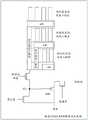
示例性的,以三层叠层CIS为例,其像素截面示意图如图2所示,三层叠层CIS包括三层叠层像素单元和CMOS像素读出电路,其信号流通方向为先经过三层叠层像素单元再经过CMOS像素读出电路,三层叠层像素单元由距离光源最近的第一层PD、与第一层PD相邻的第二层PD和与第二层PD相邻的第三层PD组成,第一层PD用于吸收蓝光,第二层PD用于吸收绿光,第三层PD用于吸收红光;其中,第一层PD包括16个PD柱,如图3(a)所示,在16个PD柱的下方设置有一个n区,该一个n区连接第一层PD的转移门连接电路,第一层PD的转移门连接电路连接CMOS像素读出电路;第二层PD包括12个PD柱和第一层PD的转移门连接电路,如图3(b)所示,在12个PD柱的下方设置有一个n区,该一个n区连接第二层PD的转移门连接电路,第二层PD的转移门连接电路连接CMOS像素读出电路;第三层PD包括8个PD柱和第一层PD的转移门连接电路、第二层PD的转移门连接电路,如图3(c)所示,在8个PD柱的下方设置有一个n区,该一个n区连接第三层PD的转移门连接电路,第三层PD的转移门连接电路连接CMOS像素读出电路;光线经过第一层PD时,基于第一层PD的共振吸收,将光线中的蓝光吸收并转换成电信号,蓝光对应的电信号经过第一层PD的转移门连接电路传输至CMOS像素读出电路,剩余光线透过第二层PD,基于第二层PD的共振吸收,将光线中的绿光吸收并转换成电信号,绿光对应的电信号经过第二层PD的转移门连接电路传输至CMOS像素读出电路,剩余光线透过第三层PD,基于第三层PD的共振吸收,将光线中的红光吸收并转换成电信号,红光对应的电信号经过第三层PD的转移门连接电路传输至CMOS像素读出电路。Illustratively, taking the three-layer CIS as an example, the schematic cross-sectional view of the pixel is shown in Figure 2. The three-layer CIS includes a three-layer pixel unit and a CMOS pixel readout circuit, and the signal flow direction is to first pass through the three-layer pixel. The unit passes through the CMOS pixel readout circuit, and the three-layer stacked pixel unit consists of the first layer PD closest to the light source, the second layer PD adjacent to the first layer PD, and the third layer PD adjacent to the second layer PD. , the first layer of PD is used to absorb blue light, the second layer of PD is used to absorb green light, and the third layer of PD is used to absorb red light; wherein, the first layer of PD includes 16 PD columns, as shown in Figure 3(a) , there is an n area under the 16 PD pillars, the n area is connected to the transfer gate connection circuit of the first layer PD, and the transfer gate connection circuit of the first layer PD is connected to the CMOS pixel readout circuit; the second layer PD includes 12 PD pillars and the transfer gate connection circuit of the first layer PD, as shown in Figure 3(b), an n area is set below the 12 PD pillars, and this n area is connected to the transfer gate connection of the second layer PD Circuit, the transfer gate connection circuit of the second layer PD is connected to the CMOS pixel readout circuit; the third layer PD includes 8 PD columns and the transfer gate connection circuit of the first layer PD, and the transfer gate connection circuit of the second layer PD, as shown in the figure As shown in 3(c), there is an n area under the 8 PD pillars, and the n area is connected to the transfer gate connection circuit of the third layer PD, and the transfer gate connection circuit of the third layer PD is connected to the CMOS pixel readout circuit. ; When the light passes through the first layer of PD, based on the resonance absorption of the first layer of PD, the blue light in the light is absorbed and converted into an electrical signal, and the electrical signal corresponding to the blue light is transmitted to the CMOS pixel through the transfer gate connection circuit of the first layer of PD. Out of the circuit, the remaining light passes through the second layer of PD. Based on the resonance absorption of the second layer of PD, the green light in the light is absorbed and converted into an electrical signal. The electrical signal corresponding to the green light is connected to the circuit through the transfer gate of the second layer of PD. It is transmitted to the CMOS pixel readout circuit, and the remaining light passes through the third layer of PD. Based on the resonance absorption of the third layer of PD, the red light in the light is absorbed and converted into an electrical signal. The electrical signal corresponding to the red light passes through the third layer of PD. The transfer gate connects the circuit to the CMOS pixel readout circuit.
可选的,所述每一层PD柱中的相邻两个PD柱之间距离为预设距离,所述第一PD柱层中PD柱的个数由所述叠层像素单元的大小和所述预设距离确定,所述第二PD柱层中PD柱的个数由所述至少一个转移门连接电路的尺寸、所述叠层像素单元的大小和所述预设距离确定。Optionally, the distance between two adjacent PD pillars in each layer of PD pillars is a preset distance, and the number of PD pillars in the first PD pillar layer is determined by the size of the stacked pixel unit and the The preset distance is determined, and the number of PD pillars in the second PD pillar layer is determined by the size of the at least one transfer gate connection circuit, the size of the stacked pixel unit, and the preset distance.
本申请实施例中,每一层PD柱中的相邻两个PD柱之间的预设距离大于或者等于50nm,由此可以避免相邻PD柱之间的相互干扰。In this embodiment of the present application, the preset distance between two adjacent PD pillars in each layer of PD pillars is greater than or equal to 50 nm, thereby avoiding mutual interference between adjacent PD pillars.
本申请实施例中,由于第一PD柱层不存在其他PD柱层对应的转移门连接电路,故,第一PD柱层中PD柱的个数由叠层像素单元的大小除以预设距离得到;由于第二PD柱层还包括至少一个转移门连接电路,故,第二PD柱层中PD柱的个数由叠层像素单元的大小减去至少一个转移门电路的尺寸之后,除以预设距离得到,具体的计算方法根据实际情况进行设置及调整,本申请实施例不做具体的限定。In the embodiment of the present application, since the first PD column layer does not have transfer gate connection circuits corresponding to other PD column layers, the number of PD columns in the first PD column layer is divided by the size of the stacked pixel unit by the preset distance Obtained: Since the second PD pillar layer further includes at least one transfer gate connection circuit, the number of PD pillars in the second PD pillar layer is divided by the size of the stacked pixel unit minus the size of the at least one transfer gate circuit and divided by The preset distance is obtained, and the specific calculation method is set and adjusted according to the actual situation, which is not specifically limited in the embodiment of the present application.
可选的,所述叠层互补金属氧化物半导体图像传感器1还包括滤色片13,其中,所述滤色片13与所述叠层像素单元10的输入端连接,所述滤色片13用于对光源的成像光信号进行过滤,得到可见光;Optionally, the stacked CMOS image sensor 1 further includes a color filter 13, wherein the color filter 13 is connected to the input end of the stacked pixel unit 10, and the color filter 13 It is used to filter the imaging light signal of the light source to obtain visible light;
所述叠层像素单元10,具体用于利用多层PD柱,从所述可见光中依次吸收RGB三色光。The stacked pixel unit 10 is specifically used for absorbing RGB three-color light from the visible light in sequence by using the multi-layer PD column.
本申请实施例中,在叠层像素单元的输入端还设置有滤色片,该滤色片用于透过可见光,过滤掉其他紫外光和红外光等杂光。In the embodiment of the present application, a color filter is further provided at the input end of the stacked pixel unit, and the color filter is used to transmit visible light and filter out other stray light such as ultraviolet light and infrared light.
可选的,滤色片为W(白色)滤光片。Optionally, the color filter is a W (white) filter.
本申请实施例中,光源发出的成像光信号经过W滤色片之后,过滤掉成像光信号中的紫外光和红外光,并透过可见光,之后,可见光依次经过多层PD柱,多层PD柱中的每一层PD柱利用各自的PD柱尺寸进行相应的共振吸收,每一层PD柱依次从可见光中吸收相应的RGB单色光。In the embodiment of the present application, after the imaging light signal emitted by the light source passes through the W color filter, ultraviolet light and infrared light in the imaging light signal are filtered out, and visible light is transmitted. Each layer of PD pillars in the pillars utilizes their respective PD pillar sizes to perform corresponding resonance absorption, and each layer of PD pillars sequentially absorbs corresponding RGB monochromatic light from visible light.
示例性的,在4个多层叠层PD柱的上方设置4个W滤色片,图4为4个W滤色片的滤色片阵列。Exemplarily, four W color filters are arranged above the four multi-layer stacked PD columns, and FIG. 4 is a color filter array of four W color filters.
可选的,所述每一层PD柱包括一个n区,所述电信号集中到所述每一层PD柱的n区。Optionally, each layer of PD pillars includes an n region, and the electrical signals are concentrated in the n regions of each layer of PD pillars.
本申请实施例中,在每一层PD柱的下方设置一个n区,该n区与转移门连接电路进行连接,每一层PD柱将光电转换之后的电信号集中到n区,并由转移门连接电路传输至CMOS像素读出电路。In the embodiment of the present application, an n area is set under each layer of PD pillars, and the n area is connected with the transfer gate connection circuit. The gate connection circuit transmits to the CMOS pixel readout circuit.
可选的,所述每一层PD柱用于吸收RGB单色光,所述每一层PD柱的尺寸由所述RGB单色光确定。Optionally, each layer of PD columns is used to absorb RGB monochromatic light, and the size of each layer of PD columns is determined by the RGB monochromatic light.
本申请实施例中,PD柱的直径是基于RGB单色光的共振波长和光信号的折射率确定的,或者通过光学模拟得到的,具体的根据实际情况进行选择,本申请实施例不做具体的限定。In the embodiment of the present application, the diameter of the PD column is determined based on the resonant wavelength of the RGB monochromatic light and the refractive index of the optical signal, or is obtained through optical simulation, and is specifically selected according to the actual situation, which is not specified in the embodiment of the present application. limited.
本申请实施例中,利用公式(1)确定PD柱的尺寸In the embodiment of the present application, the size of the PD column is determined by using the formula (1)
PD柱的尺寸=(共振波长-预设常数)/折射率(1)Size of PD column = (resonance wavelength - preset constant)/refractive index (1)
本申请实施例中,每一层PD柱吸收一种RGB单色光,当吸收绿光时,该层PD柱的直径为90nm;当吸收蓝光时,该层PD柱的直径为60nm;当吸收红光时,该层PD柱的直径为120nm。In the embodiment of the present application, each layer of PD pillars absorbs one RGB monochromatic light. When absorbing green light, the diameter of this layer of PD pillars is 90 nm; when absorbing blue light, the diameter of this layer of PD pillars is 60 nm; In red light, the diameter of the PD column in this layer is 120 nm.
可选的,所述PD柱的形状包括圆柱形和正多边形,具体的根据实际情况进行选择,本申请实施例不做具体的限定。Optionally, the shape of the PD column includes a cylindrical shape and a regular polygon, which is specifically selected according to the actual situation, which is not specifically limited in the embodiment of the present application.
可选的,所述一个CMOS像素读出电路11包括:与所述转移门连接电路12连接的转移晶体管110、与所述转移晶体管110连接的读出区111和与所述读出区111连接的放大管112;Optionally, the one CMOS pixel readout circuit 11 includes: a transfer transistor 110 connected to the transfer gate connection circuit 12 , a readout area 111 connected to the transfer transistor 110 , and a readout area 111 connected The amplifying tube 112;
所述转移晶体管110,用于将所述电信号从所述PD柱中转移至读出区,以从所述读出区读取所述电信号;the transfer transistor 110, for transferring the electrical signal from the PD column to the readout area, so as to read the electrical signal from the readout area;
所述放大管112,用于将所述读出区的电信号放大。The amplifying tube 112 is used for amplifying the electrical signal in the readout area.
本申请实施例中,转移晶体管的源极与转移门连接电路连接;所述转移晶体管的漏极与FD(读出区)连接;PD柱将电信号聚焦到转移晶体管的n+区,并经过转移晶体管转移到FD。In the embodiment of the present application, the source of the transfer transistor is connected to the transfer gate connection circuit; the drain of the transfer transistor is connected to the FD (readout area); the PD column focuses the electrical signal to the n+ area of the transfer transistor, and transfers the Transistor moved to FD.
本申请实施例中,光线在PD柱的耗尽区发生光电转换,将光信号转换成电信号,之后转移晶体管将电信号聚集到转移晶体管的n+区沟道中;并将n+区沟道中的电信号转移到FD。In the embodiment of the present application, the light is photoelectrically converted in the depletion region of the PD column, and the optical signal is converted into an electrical signal, and then the transfer transistor gathers the electrical signal into the channel of the n+ region of the transfer transistor; The signal is transferred to FD.
可选的,所述CMOS像素读出电路11还包括:与所述读出区111和所述放大管112连接的复位晶体管113;Optionally, the CMOS pixel readout circuit 11 further includes: a reset transistor 113 connected to the readout area 111 and the amplifier tube 112;
所述读出区111,还用于读出所述复位晶体管113中的复位电平;The readout area 111 is also used to read out the reset level in the reset transistor 113;
所述放大管112,还用于对所述复位电平进行放大。The amplifying tube 112 is also used for amplifying the reset level.
本申请实施例中,复位管的源极和电源连接;复位管的漏极和FD连接,其中,复位管中存储有复位电平,通过FD读出复位电平。In the embodiment of the present application, the source of the reset transistor is connected to the power supply; the drain of the reset transistor is connected to the FD, wherein the reset transistor stores the reset level, and the reset level is read out through the FD.
本申请实施例中,分别从复位管读出复位电平、从转移晶体管读出电信号,之后,对复位电平和电信号进行放大之后,对放大的电信号和放大的复位电平进行相关双采样,从而降低读出电信号的噪声。In the embodiment of the present application, the reset level is read out from the reset transistor and the electrical signal is read out from the transfer transistor, respectively, and after the reset level and the electrical signal are amplified, the amplified electrical signal and the amplified reset level are correlated and compared. sampling, thereby reducing the noise of the readout electrical signal.
如图5所示,为单个像素单元电路的简化示意图,其中,以叠层像素单元的吸收蓝光的PD柱层为例,吸收蓝光的PD柱对应的转移门连接电路和转移晶体管的源极连接,转移晶体管的漏极与FD连接;FD还与复位管的漏极连接,复位管的源极和电源连接;FD还与BSF的栅极连接,BSF的源极和电源连接,BSF的漏极与选通管的源极连接,选通管的漏极和输出端连接。As shown in FIG. 5, it is a simplified schematic diagram of a single pixel unit circuit, in which, taking the blue light absorbing PD column layer of the stacked pixel unit as an example, the transfer gate connection circuit corresponding to the blue light absorbing PD column is connected to the source electrode of the transfer transistor , the drain of the transfer transistor is connected to the FD; the FD is also connected to the drain of the reset tube, the source of the reset tube is connected to the power supply; the FD is also connected to the gate of the BSF, the source of the BSF is connected to the power supply, and the drain of the BSF is connected It is connected to the source of the strobe tube, and the drain of the strobe tube is connected to the output terminal.
可以理解的是,叠层像素单元利用多层PD柱实现RGB三色光的吸收,且PD柱的尺寸均为纳米量级的,由此,减小了叠层像素单元的像素尺寸,每个像素可以获得R、G、B三个通道的信号而无需去马赛克算法,进而提高了CIS的解析力。It can be understood that the stacked pixel unit utilizes multiple layers of PD columns to achieve the absorption of RGB three-color light, and the size of the PD columns is in the nanometer order, thereby reducing the pixel size of the stacked pixel unit. The signals of the three channels of R, G, and B can be obtained without the need for a demosaicing algorithm, thereby improving the resolution of the CIS.
实施例二Embodiment 2
本申请实施例提供一种图像处理方法,应用于叠层互补金属氧化物半导体图像传感器,叠层互补金属氧化物半导体图像传感器包括叠层像素单元和与叠层像素单元的输出端连接的CMOS像素读出电路,叠层像素单元由多层PD柱组成,多层PD柱包括三种尺寸的PD柱,如图6所示,该方法可以包括:An embodiment of the present application provides an image processing method, which is applied to a stacked CMOS image sensor. The stacked CMOS image sensor includes a stacked pixel unit and a CMOS pixel connected to an output end of the stacked pixel unit. In the readout circuit, the stacked pixel unit is composed of multi-layer PD pillars, and the multi-layer PD pillar includes three sizes of PD pillars, as shown in Figure 6, the method may include:
S101、利用多层PD柱依次吸收RGB三色光,并将RGB三色光对应的光信号转换成电信号。S101 , using a multilayer PD column to sequentially absorb the RGB three-color light, and convert the optical signal corresponding to the RGB three-color light into an electrical signal.
本申请实施例提供的一种图像处理方法适用于对采集到的光信号进行图像处理,得到光信号对应的图像的场景下。An image processing method provided by an embodiment of the present application is suitable for a scenario where image processing is performed on a collected optical signal to obtain an image corresponding to the optical signal.
本申请实施例中,多层PD柱中的每一层PD柱的尺寸相同,可见光依次透过多层PD柱,多层PD柱中的每一层PD柱依次利用各自的尺寸吸收RGB单色光,并将RGB单色光进行光电转换,得到RGB单色光对应的电信号,由此,叠层像素单元通过多层PD柱吸收RGB三色光,并将RGB三色光转换为对应的电信号。In the embodiment of the present application, each layer of PD columns in the multi-layer PD columns has the same size, visible light is transmitted through the multi-layer PD columns in sequence, and each layer of PD columns in the multi-layer PD columns sequentially absorbs RGB monochromatic colors by using their respective sizes. light, and photoelectrically convert the RGB monochromatic light to obtain electrical signals corresponding to the RGB monochromatic light. Thus, the stacked pixel unit absorbs the RGB three-color light through the multi-layer PD column, and converts the RGB three-color light into corresponding electrical signals. .
在实际应用中,叠层像素单元包括三层PD柱,三层PD柱中的一层PD柱用于吸收红光、下一层PD柱用于吸收绿光、最后一层PD柱用于吸收蓝光,且三层PD柱的叠层顺序不仅限于RGB,还可以根据实际情况进行选择,本申请实施例不做具体的限定。In practical applications, the stacked pixel unit includes three layers of PD columns. One of the three layers of PD columns is used to absorb red light, the next layer of PD columns is used to absorb green light, and the last layer of PD columns is used to absorb light. Blue light, and the stacking order of the three-layer PD column is not limited to RGB, but can also be selected according to actual conditions, which is not specifically limited in the embodiment of the present application.
例如,对于圆柱形PD柱而言,当吸收绿光时,圆柱形PD柱的直径为90nm;当吸收蓝光时,圆柱形PD柱的直径为60nm;当吸收红光时,圆柱形PD柱的直径为120nm。For example, for a cylindrical PD column, when absorbing green light, the diameter of the cylindrical PD column is 90 nm; when absorbing blue light, the diameter of the cylindrical PD column is 60 nm; when absorbing red light, the diameter of the cylindrical PD column is 60 nm. The diameter is 120nm.
进一步地,每一层PD柱的厚度在80nm-500nm之间,当厚度越大则吸收率越高、吸收纯度越低,如在利用PD柱吸收蓝光的场景下,PD柱的厚度为1μm时,该PD柱吸收蓝光的吸收率达到98%,然而会吸收部分红光和绿光,导致对蓝光的吸收纯度降低。Further, the thickness of each layer of PD pillars is between 80nm and 500nm. The larger the thickness, the higher the absorption rate and the lower the absorption purity. For example, in the scenario where the PD pillar is used to absorb blue light, the thickness of the PD pillar is 1 μm. , the absorption rate of the PD column to absorb blue light reaches 98%, but it will absorb part of the red light and green light, resulting in a decrease in the absorption purity of blue light.
本申请实施例中,每一层PD柱中的相邻两个PD柱之间的预设距离大于或者等于50nm,由此可以避免相邻PD柱之间的相互干扰。In this embodiment of the present application, the preset distance between two adjacent PD pillars in each layer of PD pillars is greater than or equal to 50 nm, thereby avoiding mutual interference between adjacent PD pillars.
本申请实施例中,多层PD柱包括两种层级结构,第一种为距离光源最近的第一PD柱层,其中排布一组PD柱;第二种为多层PD柱中除第一PD柱层外的第二PD柱层,其中排布第一转移门连接电路和一组PD柱,第一转移门电路为光源和第二PD柱层之间的至少一个PD柱层对应的至少一个转移门连接电路,故,多层PD柱中的任一PD柱层对应的转移门连接电路经过该PD柱层与CMOS像素读出电路之间的每一层PD柱。In the embodiment of the present application, the multi-layer PD column includes two hierarchical structures. The first is the first PD column layer closest to the light source, in which a group of PD columns are arranged; the second is the multi-layer PD column except for the first PD column layer. A second PD column layer outside the PD column layer, wherein a first transfer gate connection circuit and a group of PD columns are arranged, and the first transfer gate circuit is at least one PD column layer corresponding to at least one PD column layer between the light source and the second PD column layer. A transfer gate connection circuit, therefore, the transfer gate connection circuit corresponding to any PD pillar layer in the multi-layer PD pillars passes through each layer of PD pillars between the PD pillar layer and the CMOS pixel readout circuit.
可选的,每一层PD柱中的相邻两个PD柱之间距离为预设距离,第一PD柱层中PD柱的个数由叠层像素单元的大小和预设距离确定,第二PD柱层中PD柱的个数由至少一个转移门连接电路的尺寸、叠层像素单元的大小和预设距离确定。Optionally, the distance between two adjacent PD pillars in each layer of PD pillars is a preset distance, and the number of PD pillars in the first PD pillar layer is determined by the size of the stacked pixel unit and the preset distance. The number of PD pillars in the two PD pillar layers is determined by the size of the at least one transfer gate connection circuit, the size of the stacked pixel unit and the preset distance.
本申请实施例中,在每一层PD柱的下方设置一个n区,该n区与转移门连接电路进行连接,每一层PD柱将光电转换之后的电信号集中到n区,并由转移门连接电路传输至CMOS像素读出电路。In the embodiment of the present application, an n area is set under each layer of PD pillars, and the n area is connected with the transfer gate connection circuit. The gate connection circuit transmits to the CMOS pixel readout circuit.
进一步地,叠层CIS还包括与叠层像素单元的输入端连接的滤色片,叠层DIS利用多层PD柱吸收RGB三色光之前,利用滤色片对光源的成像光信号进行过滤,得到可见光;相应的,叠层CIS利用多层PD柱吸收RGB三色光,包括:叠层CIS利用多层PD柱,从可见光中依次吸收RGB三色光。Further, the laminated CIS also includes a color filter connected to the input end of the laminated pixel unit, and before the laminated DIS utilizes the multi-layer PD column to absorb the RGB three-color light, the color filter is used to filter the imaging light signal of the light source to obtain Visible light; Correspondingly, the stacked CIS utilizes multiple layers of PD columns to absorb RGB three-color light, including: the stacked CIS utilizes multiple layers of PD columns to sequentially absorb RGB three-color light from visible light.
本申请实施例中,在叠层像素单元的输入端还设置有滤色片,该滤色片用于透过可见光,过滤掉其他紫外光和红外光等杂光。In the embodiment of the present application, a color filter is further provided at the input end of the stacked pixel unit, and the color filter is used to transmit visible light and filter out other stray light such as ultraviolet light and infrared light.
可选的,滤色片为W(白色)滤光片。Optionally, the color filter is a W (white) filter.
本申请实施例中,光源发出的成像光信号经过W滤色片之后,过滤掉成像光信号中的紫外光和红外光,并透过可见光,之后,可见光依次经过多层PD柱,多层PD柱中的每一层PD柱利用各自的PD柱尺寸进行相应的共振吸收,每一层PD柱依次从可见光中吸收相应的RGB单色光。In the embodiment of the present application, after the imaging light signal emitted by the light source passes through the W color filter, ultraviolet light and infrared light in the imaging light signal are filtered out, and visible light is transmitted. Each layer of PD pillars in the pillars utilizes their respective PD pillar sizes to perform corresponding resonance absorption, and each layer of PD pillars sequentially absorbs corresponding RGB monochromatic light from visible light.
示例性的,在4个多层叠层PD柱的上方设置4个W滤色片,图4为4个W滤色片的滤色片阵列。Exemplarily, four W color filters are arranged above the four multi-layer stacked PD columns, and FIG. 4 is a color filter array of four W color filters.
S102、利用CMOS像素读出电路放大电信号,并读出电信号。S102, using a CMOS pixel readout circuit to amplify the electrical signal, and read out the electrical signal.
当叠层CIS将RGB三色光对应的光信号转换成电信号之后,叠层CIS利用CMOS像素读出电路放大电信号,并读出电信号。After the stacked CIS converts the optical signals corresponding to the RGB three-color light into electrical signals, the stacked CIS uses the CMOS pixel readout circuit to amplify the electrical signals and read out the electrical signals.
本申请实施例中,一个CMOS像素读出电路包括:与多层PD柱中的每一层PD柱连接的转移晶体管、与转移晶体管连接的读出区和与读出区连接的放大管;叠层CIS利用CMOS像素读出电路放大电信号,并读出电信号的过程具体为:利用转移晶体管将电信号从每一层PD柱中转移至读出区;从读出区读取电信号;利用放大管将读出区的电信号放大。In the embodiment of the present application, a CMOS pixel readout circuit includes: a transfer transistor connected to each PD column in the multilayer PD column, a readout area connected to the transfer transistor, and an amplifier connected to the readout area; stacking The layer CIS uses the CMOS pixel readout circuit to amplify the electrical signal, and the process of reading out the electrical signal is as follows: using the transfer transistor to transfer the electrical signal from each layer of PD columns to the readout area; read the electrical signal from the readout area; The electrical signal in the readout area is amplified by an amplifier tube.
如图5所示,为单个像素单元电路的简化示意图,其中,以叠层像素单元的吸收蓝光的PD柱层为例,吸收蓝光的PD柱对应的转移门连接电路和转移晶体管的源极连接,转移晶体管的漏极与FD连接;FD还与复位管的漏极连接,复位管的源极和电源连接;FD还与BSF的栅极连接,BSF的源极和电源连接,BSF的漏极与选通管的源极连接,选通管的漏极和输出端连接。As shown in FIG. 5, it is a simplified schematic diagram of a single pixel unit circuit, in which, taking the blue light absorbing PD column layer of the stacked pixel unit as an example, the transfer gate connection circuit corresponding to the blue light absorbing PD column is connected to the source electrode of the transfer transistor , the drain of the transfer transistor is connected to the FD; the FD is also connected to the drain of the reset tube, the source of the reset tube is connected to the power supply; the FD is also connected to the gate of the BSF, the source of the BSF is connected to the power supply, and the drain of the BSF is connected It is connected to the source of the strobe tube, and the drain of the strobe tube is connected to the output terminal.
可以理解的是,叠层像素单元利用多层PD柱实现RGB三色光的吸收,且PD柱的尺寸均为纳米量级的,由此,减小了叠层像素单元的像素尺寸,每个像素可以获得R、G、B三个通道的信号而无需去马赛克算法,进而提高了CIS的解析力。It can be understood that the stacked pixel unit utilizes multiple layers of PD columns to achieve the absorption of RGB three-color light, and the size of the PD columns is in the nanometer order, thereby reducing the pixel size of the stacked pixel unit. The signals of the three channels of R, G, and B can be obtained without the need for a demosaicing algorithm, thereby improving the resolution of the CIS.
实施例三Embodiment 3
本申请实施例提供一种存储介质,其上存储有计算机程序,上述计算机可读存储介质存储有一个或者多个程序,上述一个或者多个程序可被一个或者多个处理器执行,应用于叠层互补金属氧化物半导体图像传感器1中,该计算机程序实现如实施例二所述的图像处理方法。An embodiment of the present application provides a storage medium on which a computer program is stored, the computer-readable storage medium stores one or more programs, and the one or more programs can be executed by one or more processors and applied to stacking In the layer-complementary metal-oxide-semiconductor image sensor 1, the computer program implements the image processing method described in the second embodiment.
具体来讲,本实施例中的一种图像处理方法对应的程序指令被一电子设备读取或被执行时,包括如下步骤:Specifically, when a program instruction corresponding to an image processing method in this embodiment is read or executed by an electronic device, the following steps are included:
利用多层PD柱依次吸收RGB三色光,并将所述RGB三色光对应的光信号转换成电信号;Utilize the multilayer PD column to absorb the RGB three-color light in turn, and convert the optical signal corresponding to the RGB three-color light into an electrical signal;
利用所述CMOS像素读出电路放大所述电信号,并读出所述电信号。The electrical signal is amplified by the CMOS pixel readout circuit, and the electrical signal is read out.
在本发明的实施例中,进一步地,叠层互补金属氧化物半导体图像传感器还包括与所述叠层像素单元的输入端连接的滤色片,所述利用多层PD柱吸收RGB三色光之前,上述一个或者多个程序被上述一个或者多个处理器执行,还实现以下步骤:In an embodiment of the present invention, further, the stacked CMOS image sensor further includes a color filter connected to the input end of the stacked pixel unit, before the multi-layer PD column is used to absorb the RGB three-color light , the above one or more programs are executed by the above one or more processors, and the following steps are also implemented:
利用滤色片对光源的成像光信号进行过滤,得到可见光;Use the color filter to filter the imaging light signal of the light source to obtain visible light;
相应的,所述利用多层PD柱吸收RGB三色光,上述一个或者多个程序被上述一个或者多个处理器执行,具体实现以下步骤:Correspondingly, the above-mentioned one or more programs are executed by the above-mentioned one or more processors by using the multi-layer PD column to absorb RGB three-color light, and the following steps are specifically implemented:
利用多层PD柱,从所述可见光中依次吸收RGB三色光。Using the multi-layer PD column, RGB three-color light is sequentially absorbed from the visible light.
在本发明的实施例中,进一步地,一个CMOS像素读出电路包括:与所述多层PD柱中的每一层PD柱连接的转移晶体管、与所述转移晶体管连接的读出区和与所述读出区连接的放大管;所述利用所述CMOS像素读出电路放大所述电信号,并读出所述电信号,上述一个或者多个程序被上述一个或者多个处理器执行,具体实现以下步骤:In an embodiment of the present invention, further, a CMOS pixel readout circuit includes: a transfer transistor connected to each of the multi-layer PD pillars, a readout region connected to the transfer transistor, and a transfer transistor connected to each of the multi-layer PD pillars an amplifier tube connected to the readout area; the use of the CMOS pixel readout circuit to amplify the electrical signal and read out the electrical signal, the one or more programs are executed by the one or more processors, Specifically implement the following steps:
利用所述转移晶体管将所述电信号从所述每一层PD柱中转移至读出区;using the transfer transistor to transfer the electrical signal from the PD pillars of each layer to a readout region;
从所述读出区读取所述电信号;read the electrical signal from the readout area;
利用放大管将所述读出区的电信号放大。The electrical signal in the readout area is amplified by an amplifier tube.
以上所述,仅为本申请的较佳实施例而已,并非用于限定本申请的保护范围。The above descriptions are only preferred embodiments of the present application, and are not intended to limit the protection scope of the present application.
Claims (14)
Priority Applications (1)
| Application Number | Priority Date | Filing Date | Title |
|---|---|---|---|
| CN201910859504.1ACN110572594B (en) | 2019-09-11 | 2019-09-11 | Stacked complementary metal oxide semiconductor image sensor and image processing method |
Applications Claiming Priority (1)
| Application Number | Priority Date | Filing Date | Title |
|---|---|---|---|
| CN201910859504.1ACN110572594B (en) | 2019-09-11 | 2019-09-11 | Stacked complementary metal oxide semiconductor image sensor and image processing method |
Publications (2)
| Publication Number | Publication Date |
|---|---|
| CN110572594A CN110572594A (en) | 2019-12-13 |
| CN110572594Btrue CN110572594B (en) | 2022-04-15 |
Family
ID=68779332
Family Applications (1)
| Application Number | Title | Priority Date | Filing Date |
|---|---|---|---|
| CN201910859504.1AActiveCN110572594B (en) | 2019-09-11 | 2019-09-11 | Stacked complementary metal oxide semiconductor image sensor and image processing method |
Country Status (1)
| Country | Link |
|---|---|
| CN (1) | CN110572594B (en) |
Families Citing this family (2)
| Publication number | Priority date | Publication date | Assignee | Title |
|---|---|---|---|---|
| CN111180476A (en)* | 2020-01-06 | 2020-05-19 | Oppo广东移动通信有限公司 | A laminated CIS, image processing method, storage medium and terminal device |
| CN111223882B (en)* | 2020-01-14 | 2022-08-16 | Oppo广东移动通信有限公司 | Image sensor, image processing method and storage medium |
Citations (11)
| Publication number | Priority date | Publication date | Assignee | Title |
|---|---|---|---|---|
| CN1943041A (en)* | 2004-05-27 | 2007-04-04 | 佛文恩股份有限公司 | Vertical color filter sensor group |
| CN101964352A (en)* | 2009-07-23 | 2011-02-02 | 索尼公司 | Solid-state imaging device, method of manufacturing the same, and electronic apparatus |
| CN102623476A (en)* | 2012-04-17 | 2012-08-01 | 上海中科高等研究院 | Self-Powered CMOS Image Sensor |
| CN102623475A (en)* | 2012-04-17 | 2012-08-01 | 上海中科高等研究院 | Stacked CMOS image sensor |
| CN103517045A (en)* | 2012-06-25 | 2014-01-15 | 索尼公司 | Solid-state imaging device, method for controlling the same and electronic apparatus |
| CN105556674A (en)* | 2013-09-10 | 2016-05-04 | Setech有限公司 | Solid-state imaging device |
| CN106454161A (en)* | 2015-08-10 | 2017-02-22 | 三星电子株式会社 | Method for improving image quality of image sensor |
| CN110061019A (en)* | 2019-04-23 | 2019-07-26 | Oppo广东移动通信有限公司 | Complementary metal oxide image sensor, image processing method and storage medium |
| CN110087005A (en)* | 2019-04-23 | 2019-08-02 | Oppo广东移动通信有限公司 | Color polarization CIS, image processing method and storage medium |
| CN110099227A (en)* | 2019-05-23 | 2019-08-06 | Oppo广东移动通信有限公司 | Pixel unit circuit, image processing method and storage medium |
| CN110536084A (en)* | 2019-09-10 | 2019-12-03 | Oppo广东移动通信有限公司 | Stacked CMOS image sensor and image processing method |
Family Cites Families (1)
| Publication number | Priority date | Publication date | Assignee | Title |
|---|---|---|---|---|
| US8258560B1 (en)* | 2011-02-15 | 2012-09-04 | Aptina Imaging Corporation | Image sensors with stacked photo-diodes |
- 2019
- 2019-09-11CNCN201910859504.1Apatent/CN110572594B/enactiveActive
Patent Citations (11)
| Publication number | Priority date | Publication date | Assignee | Title |
|---|---|---|---|---|
| CN1943041A (en)* | 2004-05-27 | 2007-04-04 | 佛文恩股份有限公司 | Vertical color filter sensor group |
| CN101964352A (en)* | 2009-07-23 | 2011-02-02 | 索尼公司 | Solid-state imaging device, method of manufacturing the same, and electronic apparatus |
| CN102623476A (en)* | 2012-04-17 | 2012-08-01 | 上海中科高等研究院 | Self-Powered CMOS Image Sensor |
| CN102623475A (en)* | 2012-04-17 | 2012-08-01 | 上海中科高等研究院 | Stacked CMOS image sensor |
| CN103517045A (en)* | 2012-06-25 | 2014-01-15 | 索尼公司 | Solid-state imaging device, method for controlling the same and electronic apparatus |
| CN105556674A (en)* | 2013-09-10 | 2016-05-04 | Setech有限公司 | Solid-state imaging device |
| CN106454161A (en)* | 2015-08-10 | 2017-02-22 | 三星电子株式会社 | Method for improving image quality of image sensor |
| CN110061019A (en)* | 2019-04-23 | 2019-07-26 | Oppo广东移动通信有限公司 | Complementary metal oxide image sensor, image processing method and storage medium |
| CN110087005A (en)* | 2019-04-23 | 2019-08-02 | Oppo广东移动通信有限公司 | Color polarization CIS, image processing method and storage medium |
| CN110099227A (en)* | 2019-05-23 | 2019-08-06 | Oppo广东移动通信有限公司 | Pixel unit circuit, image processing method and storage medium |
| CN110536084A (en)* | 2019-09-10 | 2019-12-03 | Oppo广东移动通信有限公司 | Stacked CMOS image sensor and image processing method |
Also Published As
| Publication number | Publication date |
|---|---|
| CN110572594A (en) | 2019-12-13 |
Similar Documents
| Publication | Publication Date | Title |
|---|---|---|
| CN110536084A (en) | Stacked CMOS image sensor and image processing method | |
| TWI742573B (en) | Solid-state imaging element, its manufacturing method, and electronic equipment | |
| WO2017199771A1 (en) | Solid-state imaging device and electronic apparatus | |
| CN211404504U (en) | Image sensor with a plurality of pixels | |
| KR102653538B1 (en) | Semiconductor device and electronic apparatus | |
| CN101281921B (en) | Solid-state imaging device and imaging device | |
| CN102334188B (en) | Solid-state imaging element, manufacturing method thereof, and electronic information device | |
| CN110225319B (en) | Image sensor, image processing method and storage medium | |
| JP5332572B2 (en) | Solid-state imaging device and electronic apparatus | |
| WO2010004683A1 (en) | Solid-state imaging device | |
| CN110504279A (en) | Polarization type CIS, image processing method, storage medium and terminal equipment | |
| EP2673805A1 (en) | Sensing of photons | |
| CN110379824A (en) | A kind of cmos image sensor and image processing method, storage medium | |
| JP2013247182A (en) | Photoelectric conversion device | |
| JP2008060476A (en) | Solid-state imaging device and electronic information device | |
| CN110572594B (en) | Stacked complementary metal oxide semiconductor image sensor and image processing method | |
| JP2007288294A (en) | Solid-state imaging device and camera | |
| JP5504382B2 (en) | Solid-state imaging device and imaging apparatus | |
| CN110740236A (en) | Image sensor, electronic device, image processing method, and storage medium | |
| CN110312088B (en) | Pixel unit circuit, image processing method and storage medium | |
| CN110445998B (en) | A color polarized CIS, image processing method, and storage medium | |
| CN111129053B (en) | Pixel unit structure of CMOS image sensor and forming method | |
| CN111193885B (en) | Polarization type image sensor, signal processing method and storage medium | |
| CN207251823U (en) | Imaging device and imaging system | |
| CN110691207A (en) | Image sensor, image processing method and storage medium |
Legal Events
| Date | Code | Title | Description |
|---|---|---|---|
| PB01 | Publication | ||
| PB01 | Publication | ||
| SE01 | Entry into force of request for substantive examination | ||
| SE01 | Entry into force of request for substantive examination | ||
| GR01 | Patent grant | ||
| GR01 | Patent grant |