CN110569143B - Decoder for memory system and method thereof - Google Patents
Decoder for memory system and method thereofDownload PDFInfo
- Publication number
- CN110569143B CN110569143BCN201910491847.7ACN201910491847ACN110569143BCN 110569143 BCN110569143 BCN 110569143BCN 201910491847 ACN201910491847 ACN 201910491847ACN 110569143 BCN110569143 BCN 110569143B
- Authority
- CN
- China
- Prior art keywords
- data
- memory
- pages
- memory device
- page
- Prior art date
- Legal status (The legal status is an assumption and is not a legal conclusion. Google has not performed a legal analysis and makes no representation as to the accuracy of the status listed.)
- Active
Links
Images


Classifications
- G—PHYSICS
- G06—COMPUTING OR CALCULATING; COUNTING
- G06F—ELECTRIC DIGITAL DATA PROCESSING
- G06F11/00—Error detection; Error correction; Monitoring
- G06F11/07—Responding to the occurrence of a fault, e.g. fault tolerance
- G06F11/08—Error detection or correction by redundancy in data representation, e.g. by using checking codes
- G06F11/10—Adding special bits or symbols to the coded information, e.g. parity check, casting out 9's or 11's
- G06F11/1008—Adding special bits or symbols to the coded information, e.g. parity check, casting out 9's or 11's in individual solid state devices
- G06F11/1068—Adding special bits or symbols to the coded information, e.g. parity check, casting out 9's or 11's in individual solid state devices in sector programmable memories, e.g. flash disk
- H—ELECTRICITY
- H03—ELECTRONIC CIRCUITRY
- H03M—CODING; DECODING; CODE CONVERSION IN GENERAL
- H03M13/00—Coding, decoding or code conversion, for error detection or error correction; Coding theory basic assumptions; Coding bounds; Error probability evaluation methods; Channel models; Simulation or testing of codes
- H03M13/03—Error detection or forward error correction by redundancy in data representation, i.e. code words containing more digits than the source words
- H03M13/05—Error detection or forward error correction by redundancy in data representation, i.e. code words containing more digits than the source words using block codes, i.e. a predetermined number of check bits joined to a predetermined number of information bits
- H03M13/11—Error detection or forward error correction by redundancy in data representation, i.e. code words containing more digits than the source words using block codes, i.e. a predetermined number of check bits joined to a predetermined number of information bits using multiple parity bits
- H03M13/1102—Codes on graphs and decoding on graphs, e.g. low-density parity check [LDPC] codes
- H03M13/1105—Decoding
- G—PHYSICS
- G06—COMPUTING OR CALCULATING; COUNTING
- G06F—ELECTRIC DIGITAL DATA PROCESSING
- G06F11/00—Error detection; Error correction; Monitoring
- G06F11/07—Responding to the occurrence of a fault, e.g. fault tolerance
- G06F11/08—Error detection or correction by redundancy in data representation, e.g. by using checking codes
- G06F11/10—Adding special bits or symbols to the coded information, e.g. parity check, casting out 9's or 11's
- G06F11/1008—Adding special bits or symbols to the coded information, e.g. parity check, casting out 9's or 11's in individual solid state devices
- G06F11/1048—Adding special bits or symbols to the coded information, e.g. parity check, casting out 9's or 11's in individual solid state devices using arrangements adapted for a specific error detection or correction feature
- G—PHYSICS
- G06—COMPUTING OR CALCULATING; COUNTING
- G06F—ELECTRIC DIGITAL DATA PROCESSING
- G06F11/00—Error detection; Error correction; Monitoring
- G06F11/07—Responding to the occurrence of a fault, e.g. fault tolerance
- G06F11/08—Error detection or correction by redundancy in data representation, e.g. by using checking codes
- G06F11/10—Adding special bits or symbols to the coded information, e.g. parity check, casting out 9's or 11's
- G06F11/1008—Adding special bits or symbols to the coded information, e.g. parity check, casting out 9's or 11's in individual solid state devices
- G06F11/1072—Adding special bits or symbols to the coded information, e.g. parity check, casting out 9's or 11's in individual solid state devices in multilevel memories
- G—PHYSICS
- G11—INFORMATION STORAGE
- G11C—STATIC STORES
- G11C29/00—Checking stores for correct operation ; Subsequent repair; Testing stores during standby or offline operation
- G11C29/04—Detection or location of defective memory elements, e.g. cell constructio details, timing of test signals
- G11C29/08—Functional testing, e.g. testing during refresh, power-on self testing [POST] or distributed testing
- G11C29/12—Built-in arrangements for testing, e.g. built-in self testing [BIST] or interconnection details
- G11C29/38—Response verification devices
- G11C29/42—Response verification devices using error correcting codes [ECC] or parity check
- G—PHYSICS
- G11—INFORMATION STORAGE
- G11C—STATIC STORES
- G11C29/00—Checking stores for correct operation ; Subsequent repair; Testing stores during standby or offline operation
- G11C29/04—Detection or location of defective memory elements, e.g. cell constructio details, timing of test signals
- G11C29/08—Functional testing, e.g. testing during refresh, power-on self testing [POST] or distributed testing
- G11C29/12—Built-in arrangements for testing, e.g. built-in self testing [BIST] or interconnection details
- G11C29/44—Indication or identification of errors, e.g. for repair
- G—PHYSICS
- G11—INFORMATION STORAGE
- G11C—STATIC STORES
- G11C29/00—Checking stores for correct operation ; Subsequent repair; Testing stores during standby or offline operation
- G11C29/52—Protection of memory contents; Detection of errors in memory contents
- H—ELECTRICITY
- H03—ELECTRONIC CIRCUITRY
- H03M—CODING; DECODING; CODE CONVERSION IN GENERAL
- H03M13/00—Coding, decoding or code conversion, for error detection or error correction; Coding theory basic assumptions; Coding bounds; Error probability evaluation methods; Channel models; Simulation or testing of codes
- H03M13/37—Decoding methods or techniques, not specific to the particular type of coding provided for in groups H03M13/03 - H03M13/35
- H03M13/3723—Decoding methods or techniques, not specific to the particular type of coding provided for in groups H03M13/03 - H03M13/35 using means or methods for the initialisation of the decoder
- H—ELECTRICITY
- H03—ELECTRONIC CIRCUITRY
- H03M—CODING; DECODING; CODE CONVERSION IN GENERAL
- H03M13/00—Coding, decoding or code conversion, for error detection or error correction; Coding theory basic assumptions; Coding bounds; Error probability evaluation methods; Channel models; Simulation or testing of codes
- H03M13/37—Decoding methods or techniques, not specific to the particular type of coding provided for in groups H03M13/03 - H03M13/35
- H03M13/3746—Decoding methods or techniques, not specific to the particular type of coding provided for in groups H03M13/03 - H03M13/35 with iterative decoding
Landscapes
- Engineering & Computer Science (AREA)
- Theoretical Computer Science (AREA)
- Physics & Mathematics (AREA)
- Probability & Statistics with Applications (AREA)
- Quality & Reliability (AREA)
- General Engineering & Computer Science (AREA)
- General Physics & Mathematics (AREA)
- Techniques For Improving Reliability Of Storages (AREA)
- Read Only Memory (AREA)
Abstract
Translated fromChinese
Description
Translated fromChinese相关申请的交叉引用Cross References to Related Applications
本申请要求于2018年6月6日提交的申请号为62/681,431的美国临时申请的优先权,其全部内容通过引用并入本文。This application claims priority to U.S. Provisional Application No. 62/681,431, filed June 6, 2018, the entire contents of which are incorporated herein by reference.
技术领域technical field
本公开的实施例涉及一种用于存储器系统的解码方案。Embodiments of the present disclosure relate to a decoding scheme for a memory system.
背景技术Background technique
计算机环境范例已经转变成可随时随地使用的普适计算系统。因此,诸如移动电话、数码相机和笔记本计算机的便携式电子装置的使用已经迅速增加。这些便携式电子装置通常使用具有存储器装置的存储器系统,即数据存储装置。数据存储装置用作便携式电子装置的主存储器装置或辅助存储器装置。The computer environment paradigm has transformed into a pervasive computing system that can be used anytime, anywhere. As a result, the use of portable electronic devices such as mobile phones, digital cameras and notebook computers has increased rapidly. These portable electronic devices typically use memory systems with memory devices, ie data storage devices. The data storage device is used as a main memory device or a secondary memory device of the portable electronic device.
由于使用存储器装置的存储器系统不具有移动部件,因此它们提供优异的稳定性、耐用性、高信息访问速度和低功耗。具有这些优点的存储器系统的示例包括通用串行总线(USB)存储器装置、诸如通用闪存(UFS)的具有各种接口的存储卡以及固态驱动器(SSD)。存储器系统可以使用各种编码器和解码器。Since memory systems using memory devices have no moving parts, they offer excellent stability, durability, high information access speed, and low power consumption. Examples of memory systems with these advantages include Universal Serial Bus (USB) memory devices, memory cards with various interfaces such as Universal Flash Memory (UFS), and Solid State Drives (SSD). Memory systems can use a variety of encoders and decoders.
发明内容Contents of the invention
本发明的方面包括存储器系统,该存储器系统包括能够提高错误校正性能并且减少解码延迟的解码器。Aspects of the invention include a memory system including a decoder capable of improving error correction performance and reducing decoding delay.
在一方面,提供一种系统,其包括存储器装置以及控制器,该存储器装置包括每个存储数据的多个页面,该控制器包括解码器。控制器从存储器装置接收数据,并且基于多个页面之中的存储该数据的页面的类型以及指示存储器装置在其生命周期中的当前状态的生命周期信息来解码数据。In one aspect, a system is provided that includes a memory device that includes multiple pages each storing data, and a controller that includes a decoder. A controller receives data from a memory device and decodes the data based on a type of a page storing the data among a plurality of pages and life cycle information indicating a current state of the memory device in its life cycle.
在另一方面,提供一种操作系统的方法,该系统包括存储器装置,该存储器装置包括每个存储数据的多个页面。该方法包括从存储器装置接收数据,并且基于多个页面之中的存储该数据的页面的类型以及指示存储器装置在其寿命周期中的当前状态的寿命周期信息来解码数据。In another aspect, a method of operating an system is provided that includes a memory device including a plurality of pages each storing data. The method includes receiving data from a memory device and decoding the data based on a type of a page storing the data among a plurality of pages and life cycle information indicative of a current state of the memory device in its life cycle.
从以下描述中,本发明的其它方面将变得显而易见。Other aspects of the invention will become apparent from the following description.
附图说明Description of drawings
图1是示出根据本发明的实施例的数据处理系统的框图。FIG. 1 is a block diagram illustrating a data processing system according to an embodiment of the present invention.
图2是示出根据本发明的实施例的存储器系统的框图。FIG. 2 is a block diagram illustrating a memory system according to an embodiment of the present invention.
图3是示出根据本发明的实施例的存储器装置的存储块的电路图。FIG. 3 is a circuit diagram illustrating a memory block of a memory device according to an embodiment of the present invention.
图4是示出存储器装置的不同类型单元的状态分布的示图。FIG. 4 is a diagram showing the state distribution of different types of cells of a memory device.
图5是示出存储器装置中的不同页面的失败位分布的示图。FIG. 5 is a diagram showing fail bit distributions of different pages in a memory device.
图6是示出根据本发明的实施例的存储器系统的示图。FIG. 6 is a diagram illustrating a memory system according to an embodiment of the present invention.
图7是示出根据本发明的实施例的解码器的示图。FIG. 7 is a diagram illustrating a decoder according to an embodiment of the present invention.
图8是示出根据本发明的实施例的存储装置的示图。FIG. 8 is a diagram illustrating a storage device according to an embodiment of the present invention.
图9是示出根据本发明的实施例的低密度奇偶校验(LDPC)解码器的示图。FIG. 9 is a diagram illustrating a Low Density Parity Check (LDPC) decoder according to an embodiment of the present invention.
图10是示出根据本发明的实施例的解码器的操作的流程图。FIG. 10 is a flowchart illustrating the operation of a decoder according to an embodiment of the present invention.
具体实施方式Detailed ways
下面参照附图更详细地描述各个实施例。然而,本发明可以不同的形式实现并且因此不应被解释为限于本文阐述的实施例。相反,提供这些实施例使得本公开彻底且完整,并且向本领域技术人员充分传达本发明的范围。此外,本文对“实施例”、“另一实施例”等的参考不一定仅针对一个实施例,并且对任意这种短语的不同参考不一定针对相同的实施例。在整个公开中,相同的附图标记在本发明的附图和实施例中表示相同的部件。Various embodiments are described in more detail below with reference to the accompanying drawings. However, this invention may be embodied in different forms and therefore should not be construed as limited to the embodiments set forth herein. Rather, these embodiments are provided so that this disclosure will be thorough and complete, and will fully convey the scope of the invention to those skilled in the art. Furthermore, references herein to "an embodiment," "another embodiment," etc. are not necessarily to only one embodiment, and different references to any such phrase are not necessarily to the same embodiment. Throughout the disclosure, like reference numerals refer to like parts in the drawings and embodiments of the present invention.
本发明可以以多种方式来实施,包括作为进程;设备;系统;在计算机可读存储介质上实现的计算机程序产品;和/或处理器,诸如适于运行存储在联接至处理器的存储器上和/或由联接至处理器的存储器提供的指令的处理器。在本说明书中,这些实施方式或本发明可以采用的任意其它形式可以被称为技术方案。通常,可以在本发明的范围内改变所公开的进程的步骤的顺序。除非另有说明,否则被描述为适于执行任务的、诸如处理器或存储器的组件可以被实施为临时配置为在给定时间执行该任务的通用组件或者被制造为执行该任务的专用组件。如本文所使用的,术语“处理器”等是指适于处理诸如计算机程序指令的数据的一个或多个装置、电路和/或处理内核。The invention can be implemented in numerous ways, including as a process; an apparatus; a system; a computer program product embodied on a computer-readable storage medium; and/or a processor, such as one adapted to execute the and/or instructions provided by a memory coupled to the processor. In this specification, these implementations or any other form that the present invention can take may be referred to as technical solutions. In general, the order of the steps of disclosed processes may be altered within the scope of the invention. Unless otherwise stated, a component described as adapted to perform a task, such as a processor or memory, may be implemented as a general-purpose component temporarily configured to perform that task at a given time or as a dedicated component manufactured to perform that task. As used herein, the terms "processor" and the like refer to one or more devices, circuits and/or processing cores adapted to process data, such as computer program instructions.
以下与示出本发明的方面的附图一起提供本发明的实施例的详细描述。结合这些实施例来描述本发明,但是本发明不限于任意实施例。本发明的范围仅由权利要求限定。本发明涵盖在权利要求范围内的许多替换方案、修改方案和等同方案。在以下描述中阐述了许多具体细节,以便提供对本发明的透彻理解。提供这些细节是为了示例的目的;可以在没有一些或全部这些具体细节的情况下根据权利要求来实践本发明。为清楚起见,没有详细描述与本发明相关的技术领域中已知的技术材料,以免不必要地模糊本发明。A detailed description of embodiments of the invention is provided below along with accompanying figures that illustrate aspects of the invention. The present invention is described in conjunction with these embodiments, but the present invention is not limited to any embodiment. The scope of the invention is limited only by the claims. The invention encompasses numerous alternatives, modifications and equivalents within the scope of the claims. In the following description, numerous specific details are set forth in order to provide a thorough understanding of the present invention. These details are provided for the purpose of example; the invention may be practiced according to the claims without some or all of these specific details. For the purpose of clarity, technical material that is known in the technical fields related to the invention has not been described in detail so that the invention is not unnecessarily obscured.
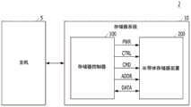
图1是示出根据本发明的实施例的数据处理系统2的框图。FIG. 1 is a block diagram illustrating a
参照图1,数据处理系统2可包括主机装置5和存储器系统10。存储器系统10可以从主机装置5接收请求并且响应于所接收的请求而操作。例如,存储器装置10可以存储待由主机装置5访问的数据。Referring to FIG. 1 ,
主机装置5可以利用各种电子装置中的任意一种来实施。在各个实施例中,主机装置5可以包括诸如下列的电子装置:台式计算机、工作站、三维(3D)电视、智能电视、数字音频记录器、数字音频播放器、数字图片记录器、数字图片播放器和/或数字视频记录器和数字视频播放器。在各个实施例中,主机装置5可以包括诸如下列的便携式电子装置:移动电话、智能电话、电子书、MP3播放器、便携式多媒体播放器(PMP)和/或便携式游戏机。The host device 5 may be implemented using any of various electronic devices. In various embodiments, host device 5 may include electronic devices such as desktop computers, workstations, three-dimensional (3D) televisions, smart televisions, digital audio recorders, digital audio players, digital picture recorders, digital picture players and/or digital video recorders and digital video players. In various embodiments, the host device 5 may include a portable electronic device such as a mobile phone, a smart phone, an electronic book, an MP3 player, a portable multimedia player (PMP), and/or a portable game console.
存储器系统10可以利用诸如固态驱动器(SSD)和存储卡的各种存储装置中的任意一种来实施。在各个实施例中,存储器系统10可以被设置为诸如下列的电子装置中的各种组件中的一种:计算机、超移动个人计算机(PC)(UMPC)、工作站、上网本计算机、个人数字助理(PDA)、便携式计算机、网络平板PC、无线电话、移动电话、智能电话、电子书阅读器、便携式多媒体播放器(PMP)、便携式游戏装置、导航装置、黑盒、数码相机、数字多媒体广播(DMB)播放器、三维电视、智能电视、数字音频记录器、数字音频播放器、数字图片记录器、数字图片播放器、数字视频记录器、数字视频播放器、数据中心的存储装置、能够在无线环境中接收和发送信息的装置、射频识别(RFID)装置、以及家庭网络的各种电子装置中的一种、计算机网络的各种电子装置中的一种、远程信息处理网络的电子装置中的一种或计算系统的各种组件中的一种。
存储器系统10可以包括存储器控制器100和半导体存储器装置200,在下文中半导体存储器装置200有时也被简称为存储器装置。存储器控制器100可以控制半导体存储器装置200的全部操作。The
半导体存储器装置200可以在存储器控制器100的控制下执行一个或多个擦除操作、编程操作和读取操作。半导体存储器装置200可以通过输入/输出线来接收命令CMD、地址ADDR和数据DATA。半导体存储器装置200可以通过电源线接收电力PWR,并且通过控制线接收控制信号CTRL。根据存储器系统10的设计和配置,控制信号CTRL可以包括命令锁存使能信号、地址锁存使能信号、芯片使能信号、写入使能信号、读取使能信号以及其它操作信号。The
存储器控制器100和半导体存储器装置200可以被集成在诸如固态驱动器(SSD)的单个半导体装置中。SSD可以包括用于将数据存储在其中的存储装置。当存储器系统10用于SSD中时,联接至存储器系统10的主机装置(例如,图1的主机装置5)的操作速度可以得到显著提高。The
存储器控制器100和半导体存储器装置200可以被集成在诸如存储卡的单个半导体装置中。例如,存储器控制器100和半导体存储器装置200可以被如此集成以配置:个人计算机存储卡国际协会(PCMCIA)的个人计算机(PC)卡、紧凑式闪存(CF)卡、智能媒体(SM)卡、记忆棒、多媒体卡(MMC)、尺寸减小的多媒体卡(RS-MMC)、微尺寸版本的MMC(微型MMC)、安全数字(SD)卡、迷你安全数字(迷你SD)卡、微型安全数字(微型SD)卡、安全数字高容量(SDHC)和/或通用闪存(UFS)。The
图2是示出根据本发明的实施例的存储器系统的框图。例如,图2的存储器系统可以描绘图1中所示的存储器系统10。FIG. 2 is a block diagram illustrating a memory system according to an embodiment of the present invention. For example, the memory system of FIG. 2 may depict the
参照图2,存储器系统10可以包括存储器控制器100和半导体存储器装置200。存储器系统10可以响应于来自主机装置(例如,图1的主机装置5)的请求而操作,并且特别地,存储待由主机装置访问的数据。Referring to FIG. 2 , a
存储器装置200可以存储待由主机装置访问的数据。
存储器装置200可以利用诸如动态随机存取存储器(DRAM)和/或静态随机存取存储器(SRAM)的易失性存储器装置或者诸如下列的非易失性存储器装置来实施:只读存储器(ROM)、掩模ROM(MROM)、可编程ROM(PROM)、可擦除可编程ROM(EPROM)、电可擦除可编程ROM(EEPROM)、铁电随机存取存储器(FRAM)、相变RAM(PRAM)、磁阻RAM(MRAM)和/或电阻式RAM(RRAM)。
控制器100可以控制数据在存储器装置200中的存储。例如,控制器100可以响应于来自主机装置的请求来控制存储器装置200。控制器100可以将从存储器装置200读取的数据提供至主机装置,并且可以将从主机装置提供的数据存储至存储器装置200中。The
控制器100可以包括通过总线160联接的存储装置110、控制组件120、错误校正码(ECC)组件130、主机接口(I/F)140和存储器接口(I/F)150,控制组件120可被实施为诸如中央处理单元(CPU)的处理器。The
存储装置110可以用作存储器系统10和控制器100的工作存储器,并且存储用于驱动存储器系统10和控制器100的数据。当控制器100控制存储器装置200的操作时,存储装置110可以存储控制器100和存储器装置200为诸如读取操作、写入操作、编程操作和擦除操作的操作所使用的数据。The storage device 110 may serve as a working memory of the
存储装置110可以利用诸如静态随机存取存储器(SRAM)或动态随机存取存储器(DRAM)的易失性存储器来实施。如上所述,存储装置110可以将由主机装置使用的数据存储在存储器装置200中以用于读取操作和写入操作。为了存储数据,存储装置110可以包括程序存储器、数据存储器、写入缓冲器、读取缓冲器、映射缓冲器等。The storage device 110 may be implemented using volatile memory such as static random access memory (SRAM) or dynamic random access memory (DRAM). As described above, the storage device 110 may store data used by the host device in the
控制组件120可以控制存储器系统10的一般操作,并且响应于来自主机装置的写入请求或读取请求,控制对存储器装置200的写入操作或读取操作。控制组件120可以驱动被称为闪存转换层(FTL)的固件,以控制存储器系统10的一般操作。例如,FTL可以执行诸如逻辑至物理(L2P)映射、损耗均衡、垃圾收集和/或坏块处理的操作。L2P映射也被称为逻辑块寻址(LBA)。The control component 120 may control general operations of the
在读取操作期间,ECC组件130可以检测并校正从存储器装置200读取的数据中的错误。当错误位的数量大于或等于可校正错误位的阈值数量时,ECC组件130可以不校正错误位,而是可以输出指示校正错误位失败的错误校正失败信号。During a read operation, the
在各个实施例中,ECC组件130可以基于诸如下列的编码调制来执行错误校正操作:低密度奇偶校验(LDPC)码、博斯-查德胡里-霍昆格姆(Bose-Chaudhuri-Hocquenghem,BCH)码、turbo码、turbo乘积码(TPC)、里德-所罗门(Reed-Solomon,RS)码、卷积码、递归系统码(RSC)、网格编码调制(TCM)或分组编码调制(BCM)。然而,错误校正不限于这些技术。因此,ECC组件130可以包括用于合适的错误校正操作的任意和所有电路、系统或装置。In various embodiments, the
主机接口140可以通过诸如下列的各种接口协议中的一种或多种与主机装置通信:通用串行总线(USB)、多媒体卡(MMC)、高速外围组件互连(PCI-e或PCIe)、小型计算机系统接口(SCSI)、串列SCSI(SAS)、串行高级技术附件(SATA)、并行高级技术附件(PATA)、增强型小型磁盘接口(ESDI)和电子集成驱动器(IDE)。
存储器接口150可以提供控制器100和存储器装置200之间的接口,以允许控制器100响应于来自主机装置的请求来控制存储器装置200。存储器接口150可以在控制组件120的控制下生成用于存储器装置200的控制信号并且处理数据。当存储器装置200是诸如NAND闪速存储器的闪速存储器时,存储器接口150可以在控制组件120的控制下生成用于存储器的控制信号并且处理数据。The
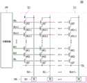
存储器装置200可以包括存储器单元阵列210、控制电路220、电压生成电路230、行解码器240、可以是页面缓冲器阵列形式的页面缓冲器250、列解码器260以及输入和输出(输入/输出)电路270。存储器单元阵列210可以包括可存储数据的多个存储块211。电压生成电路230、行解码器240、页面缓冲器250、列解码器260和输入/输出电路270可以形成存储器单元阵列210的外围电路。外围电路可以执行对存储器单元阵列210的编程操作、读取操作或者擦除操作。控制电路220可以控制外围电路。
电压生成电路230可以生成各种电平的操作电压。例如,在擦除操作中,电压生成电路230可以生成诸如擦除电压和通过电压的各种电平的操作电压。The
行解码器240可以与电压生成电路230和多个存储块211电通信。行解码器240可以响应于由控制电路220生成的行地址而在多个存储块211之中选择至少一个存储块,并且将从电压生成电路230供应的操作电压传送至所选择的存储块。The
页面缓冲器250可以通过位线BL(图3中示出)与存储器单元阵列210联接。页面缓冲器250可以响应于由控制电路220生成的页面缓冲器控制信号,利用正电压对位线BL预充电,在编程操作中将数据传送至所选择的存储块并且在读取操作中从所选择的存储块接收数据,或临时存储所传送的数据。The
列解码器260可以将数据传送至页面缓冲器250并且从页面缓冲器250接收数据,或将数据传送至输入/输出电路270并且从输入/输出电路270接收数据。
输入/输出电路270可以将从外部装置(例如,图1的存储器控制器100)接收的命令和地址传送至控制电路220,并且通过输入/输出电路270将数据从外部装置传送至列解码器260,或将数据从列解码器260输出至外部装置。The input/
控制电路220可以响应于命令和地址来控制外围电路。The
图3是示出根据本发明的实施例的半导体存储器装置的存储块的电路图。例如,图3的存储块可以是图2中所示的存储器单元阵列210的存储块211中的任意一个。FIG. 3 is a circuit diagram showing a memory block of a semiconductor memory device according to an embodiment of the present invention. For example, the memory block of FIG. 3 may be any one of the memory blocks 211 of the
参照图3,示例性存储块211可以包括联接至行解码器240的多个字线WL0至WLn-1、漏极选择线DSL和源极选择线SSL。这些线并联行地布置,并且多个字线在DSL和SSL之间。Referring to FIG. 3 , an
示例性存储块211可以进一步包括分别联接至位线BL0至BLm-1的多个单元串221。每列的单元串可以包括一个或多个漏极选择晶体管DST和一个或多个源极选择晶体管SST。在所示的实施例中,每个单元串具有一个DST和一个SST。在单元串中,多个存储器单元或存储器单元晶体管MC0至MCn-1可以串联联接在选择晶体管DST和SST之间。存储器单元中的每一个可以形成为多个层单元。例如,存储器单元中的每一个可以形成为存储1位数据的单层单元(SLC)。存储器单元中的每一个可以形成为存储2位数据的多层单元(MLC)。存储器单元中的每一个可以形成为存储3位数据的三层单元(TLC)。存储器单元中的每一个可以形成为存储4位数据的四层单元(QLC)。The
每个单元串中的SST的源极可以联接至公共源极线CSL,并且每个DST的漏极可以联接至相应位线。单元串中的SST的栅极可以联接至SSL,并且单元串中的DST的栅极可以联接至DSL。横跨单元串的存储器单元的栅极可以联接至各自的字线。也就是说,存储器单元MC0的栅极联接至相应字线WL0,存储器单元MC1的栅极联接至相应字线WL1,等等。联接至特定字线的一组存储器单元可以被称为物理页面。因此,存储块211中的物理页面的数量可以对应于字线的数量。The sources of the SSTs in each cell string may be coupled to a common source line CSL, and the drains of each DST may be coupled to a corresponding bit line. The gates of the SSTs in the string may be coupled to the SSL, and the gates of the DSTs in the string may be coupled to the DSL. The gates of the memory cells across the string may be coupled to respective word lines. That is, the gate of the memory cell MC0 is coupled to the corresponding word line WL0, the gate of the memory cell MC1 is coupled to the corresponding word line WL1, and so on. A group of memory cells coupled to a particular word line may be referred to as a physical page. Accordingly, the number of physical pages in the
页面缓冲器250可以包括联接至位线BL0至BLm-1的多个页面缓冲器251。页面缓冲器251可以响应于页面缓冲器控制信号而操作。例如,在读取或验证操作期间,页面缓冲器251可以临时存储通过位线BL0至BLm-1接收的数据或者感测位线的电压或电流。The
在一些实施例中,存储块211可以包括NAND型闪速存储器单元。然而,存储块211不限于这种单元类型,而是可以包括NOR型闪速存储器单元。存储器单元阵列210可以被实施为组合两种或更多种类型的存储器单元的混合闪速存储器,或者控制器嵌入在存储器芯片内的1-NAND闪速存储器。In some embodiments,
诸如闪速存储器的存储器装置可以通过使用编程操作将单元调制到不同的状态或电压电平来在每单元中存储多个位。Memory devices such as flash memory can store multiple bits per cell by modulating the cells to different states or voltage levels using a programming operation.
图4是示出存储器装置的不同类型单元的编程状态或电压(PV)电平的分布的示图。4 is a graph showing the distribution of programmed states or voltage (PV) levels of different types of cells of a memory device.
参照图4,存储块的存储器单元中的每一个可以利用例如以下的多个层单元来实施:存储1位数据的单层单元(SLC)、存储2位数据的多层单元(MLC)、存储3位数据的三层单元(TLC)或存储4位数据的四层单元(QLC)。Referring to FIG. 4 , each of the memory cells of the storage block may be implemented using a plurality of layer cells such as the following: a single-level cell (SLC) storing 1-bit data, a multi-level cell (MLC) storing 2-bit data, storing Triple-Level Cell (TLC) for 3-bit data or Quad-Level Cell (QLC) for 4-bit data.
每个SLC可以包括两种状态P0和P1。P0可以指示擦除状态,并且P1可以指示编程状态。由于SLC可以被设定为两种不同状态中的一种,因此每个SLC可以根据设定编码方法来编程或存储1个位。每个MLC可以包括四种状态P0、P1、P2和P3。在这些状态之中,P0可以指示擦除状态,并且P1至P3可以指示编程状态。由于MLC可以被设定为四种不同状态中的一种,因此每个MLC可以根据设定编码方法来编程或存储两个位。每个TLC可以包括八种状态P0至P7。在这些状态之中,P0可以指示擦除状态,并且P1至P7可以指示编程状态。由于TLC可以被设定为八种不同状态中的一种,因此每个TLC可以根据设定编码方法来编程或存储三个位。每个QLC可以包括16种状态P0至P15。在这些状态之中,P0可以指示擦除状态,并且P1至P15可以指示编程状态。由于QLC可以被设定为16种不同状态中的一种,因此每个QLC可以根据设定编码方法来编程或存储四个位。Each SLC can include two states P0 and P1. P0 may indicate an erased state, and P1 may indicate a programmed state. Since SLCs can be set to one of two different states, each SLC can be programmed or stored with 1 bit depending on the set encoding method. Each MLC can include four states P0, P1, P2 and P3. Among these states, P0 may indicate an erase state, and P1 to P3 may indicate a program state. Since MLCs can be set to one of four different states, each MLC can be programmed or stored with two bits depending on the set encoding method. Each TLC can include eight states P0 to P7. Among these states, P0 may indicate an erased state, and P1 to P7 may indicate a programmed state. Since TLCs can be set to one of eight different states, each TLC can be programmed or stored with three bits depending on the set encoding method. Each QLC can include 16 states P0 to P15. Among these states, P0 may indicate an erase state, and P1 to P15 may indicate a program state. Since QLCs can be programmed into one of 16 different states, each QLC can be programmed or stored with four bits depending on the programmed encoding method.
目前,多层单元(例如,MLC、TLC、QLC)数据编码广泛用于存储器装置(例如,NAND闪速存储器)以增加诸如SSD的存储器系统的容量。存储器装置的字线包括多个逻辑页面。例如,MLC存储器的字线具有两个逻辑页面:最高有效位(MSB)页面和最低有效位(LSB)页面。TLC存储器的字线具有三个逻辑页面:MSB页面、中间有效位(CSB)页面和LSB页面。QLC存储器的字线具有四个逻辑页面:MSB页面、中间最高有效位(CMSB)页面、中间最低有效位(CLSB)页面和LSB页面。如上所述,存储器装置的不同类型页面具有不同的读取阈值电压。因此,如图5中所示,不同的类型页面具有不同的失败位分布。Currently, multi-level cell (eg, MLC, TLC, QLC) data encoding is widely used in memory devices (eg, NAND flash memory) to increase the capacity of memory systems such as SSDs. A word line of a memory device includes a plurality of logical pages. For example, a word line of an MLC memory has two logical pages: a most significant bit (MSB) page and a least significant bit (LSB) page. A word line of a TLC memory has three logical pages: MSB page, center significant bit (CSB) page and LSB page. A word line of a QLC memory has four logical pages: MSB page, middle most significant bit (CMSB) page, middle least significant bit (CLSB) page and LSB page. As mentioned above, different types of pages of a memory device have different read threshold voltages. Therefore, as shown in FIG. 5, different types of pages have different failure bit distributions.
图5是示出针对存储器装置,例如三层单元(TLC)NAND闪速存储器装置中的不同类型页面的失败位分布的示图。5 is a graph showing fail bit distributions for different types of pages in a memory device, such as a triple level cell (TLC) NAND flash memory device.
参照图5,X轴表示在解码期间失效的位的数量,即每页面(例如,4KB的数据)的失败位(FB)计数,并且Y轴表示失败位计数的概率分布函数(PDF)。如图5所示,TLC NAND闪速存储器的MSB、CSB和LSB页面中的每一个具有不同的失败位分布。此外,失败位分布可以基于TLC NAND闪速存储器或包括TLC NAND闪速存储器的存储器系统在其寿命周期或使用寿命内的当前状态而变化。Referring to FIG. 5 , the X-axis represents the number of failed bits during decoding, that is, the failed bit (FB) count per page (for example, 4KB of data), and the Y-axis represents the probability distribution function (PDF) of the failed bit count. As shown in Figure 5, each of the MSB, CSB and LSB pages of TLC NAND flash memory has a different fail bit distribution. Furthermore, the failure bit distribution may vary based on the current state of the TLC NAND flash memory or a memory system including the TLC NAND flash memory during its lifetime or useful life.
图6是示出根据本发明的实施例的存储器系统的示图。FIG. 6 is a diagram illustrating a memory system according to an embodiment of the present invention.
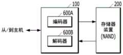
参照图6,存储器系统可以包括控制器100和存储器装置200。存储器装置200可以包括具有诸如单层单元(SLC)、多层单元(MLC)、三层单元(TLC)和/或四层单元(QLC)的存储器单元的NAND闪速存储器装置。在各个实施例中,存储器装置200可以包括具有TLC存储器单元(即,TLC)或QLC存储器单元(即,QLC)的NAND型闪速存储器装置。Referring to FIG. 6 , a memory system may include a
控制器100可以从主机接收命令,并且向存储器装置200提供所接收的命令。例如,控制器100接收写入命令和对应于写入命令的写入数据,并且控制存储器装置200对写入数据执行编程操作。再例如,控制器100接收读取命令,并且控制存储器装置200对与读取命令相对应的数据执行读取操作。控制器100将对应于读取命令的读取数据传送至主机。The
控制器100可以包括编码器600A和解码器600B。在编程操作期间,编码器600A可以基于设定编码方案对写入数据执行编码操作。在读取操作期间,解码器600B可以基于对应于编码方案的设定解码方案对读取数据执行解码操作。控制器100和存储器装置200可以执行图1和图2中描述的操作。在实施例中,编码器600A和解码器600B可以被实现在图2中所示的控制器100的ECC组件130中。如下所述,也可以采用其它合适的布置。通常,编码器600A和解码器600B可以通过硬件、软件、固件或其任何合适的组合来实施。The
解码器600B可以基于诸如下列的各种码来执行解码操作:低密度奇偶校验(LDPC)码、博斯-查德胡里-霍昆格姆(Bose-Chaudhuri-Hocquenghem,BCH)码、turbo码、turbo乘积码(TPC)、里德-所罗门(Reed-Solomon,RS)码、卷积码、递归系统码(RSC)、网格编码调制(TCM)或分组编码调制(BCM)。在各个实施例中,解码器600B可以利用使用LDPC码的LDPC解码器来实施。LDPC码是奇偶校验矩阵可以由低密度奇偶校验矩阵表示的一类(a familyof)线性块前向错误校正码(ECC)。LDPC码提供优异的错误校正性能。The
解码器600B(例如,LDPC解码器)可以具有用于调谐解码算法以实现最佳错误校正性能的一些参数。这些参数可以不仅取决于奇偶校验矩阵的结构,而且还取决于失败位分布、原始位错误率(BER)和其它因素。因此,当将解码算法应用于来自存储器装置200的不同逻辑页面的数据时,用于某个类型页面(例如,MSB页面)的最佳参数可以与用于其它类型页面(例如,CSB页面和LSB页面)的最佳参数不同。此外,用于某个类型页面的最佳参数可以基于存储器装置200在其寿命周期中的当前状态而变化。例如,在存储器装置200的寿命初期时的用于MSB页面的最佳参数可以与在存储器装置200的寿命末期时的用于MSB页面的最佳参数不同。
在各个实施例中,解码器600B可以获得存储所接收的数据的页面的类型,即页面类型。例如,解码器600B获得标识存储数据的页面的类型的页面类型信息。可以从读取命令中提取页面类型信息。此外,解码器600B可以分别获得关于页面类型的失败位分布和/或原始位错误率(BER)的信息。可以从先前解码结果导出或获得这样的信息。基于页面类型以及关于该页面类型的失败位分布和/或原始BER的信息,解码器600B可以在多个参数组之中选择参数组,并且基于所选择的参数组中的参数执行解码过程。In various embodiments, the
图7是示出根据本发明的实施例的解码器的示图。例如,图7的解码器可以描绘图6中所示的解码器600B。FIG. 7 is a diagram illustrating a decoder according to an embodiment of the present invention. For example, the decoder of FIG. 7 may depict
参照图7,解码器600B可以包括存储装置710、选择器720和解码引擎730。解码引擎730可以接收数据并且解码所接收的数据以生成经解码数据。此外,解码引擎730可以基于解码方案(例如,低密度奇偶校验(LDPC)方案)对读取数据执行解码操作。Referring to FIG. 7 , a
在各个实施例中,解码引擎730可以从存储器装置(例如,图6的存储器装置200)接收读取数据。存储器装置200可包括如上所述的定义逻辑页面的多个存储器单元,诸如三层单元(TLC)或四层单元(QLC)。在利用TLC实施的存储器装置中,页面的类型可以包括最高有效位(MSB)页面、中间有效位(CSB)页面和最低有效位(LSB)页面。在利用QLC实施的存储器装置中,页面的类型可以包括MSB页面、中间最高有效位(CMSB)页面、中间最低有效位(CLSB)页面和LSB页面。In various embodiments,
图8是示出根据本发明的实施例的存储装置的示图。例如,图8的存储装置可以描绘图7中所示的存储装置710。FIG. 8 is a diagram illustrating a storage device according to an embodiment of the present invention. For example, the memory device of FIG. 8 may depict the
参照图8,存储装置710可以存储用于解码方案(例如,低密度奇偶校验(LDPC)方案)的多个参数组PG11至PGmn。多个参数组PG11至PGmn可以针对m个页面类型和存储器装置200的寿命周期中的n个时间点而包括(m×n)个参数组。Referring to FIG. 8 , the
参数组PG11对应于第一页面类型PAGE1和寿命周期中的第一时间点LIFE CYCLE1的组合,参数组PG12对应于第一页面类型PAGE1和寿命周期中的第二时间点LIFE CYCLE2的组合,并且参数组PG1n对应于第一页面类型PAGE1和寿命周期中的第n时间点LIFE CYCLEn的组合。参数组PG21对应于第二页面类型PAGE2和寿命中的第一时间点LIFE CYCLE1的组合,参数组PG22对应于第二页面类型PAGE2和寿命周期中的第二时间点LIFE CYCLE2的组合,并且参数组PG2n对应于第二页面类型PAGE2和寿命周期中的第n时间点LIFE CYCLEn的组合。参数组PGm1对应于第m页面类型PAGEm和寿命周期中的第一时间点LIFE CYCLE1的组合,参数组PGm2对应于第m页面类型PAGEm和寿命周期中的第二时间点LIFE CYCLE2的组合,并且参数组PGmn对应于第m页面类型PAGEm和寿命周期中的第n时间点LIFE CYCLEn的组合。The parameter group PG11 corresponds to the combination of the first page type PAGE1 and the first time point LIFE CYCLE1 in the life cycle, the parameter group PG12 corresponds to the combination of the first page type PAGE1 and the second time point LIFE CYCLE2 in the life cycle, and the parameter The group PG1n corresponds to the combination of the first page type PAGE1 and the nth time point LIFE CYCLEn in the life cycle. The parameter group PG21 corresponds to the combination of the second page type PAGE2 and the first time point LIFE CYCLE1 in the life cycle, the parameter group PG22 corresponds to the combination of the second page type PAGE2 and the second time point LIFE CYCLE2 in the life cycle, and the parameter group PG2n corresponds to the combination of the second page type PAGE2 and the nth time point LIFE CYCLEn in the life cycle. The parameter group PGm1 corresponds to the combination of the mth page type PAGEm and the first time point LIFE CYCLE1 in the life cycle, the parameter group PGm2 corresponds to the combination of the mth page type PAGEm and the second time point LIFE CYCLE2 in the life cycle, and the parameter The group PGmn corresponds to a combination of the mth page type PAGEm and the nth time point LIFE CYCLEn in the life cycle.
在实施例中,m是3,这表示3种不同页面类型:MSB页面、CSB页面和LSB页面。可选地,在另一实施例中,m可以是4,这表示4种不同页面类型:MSB页面、CMSB页面、CLSB页面和LSB页面。In an embodiment, m is 3, which means 3 different page types: MSB page, CSB page and LSB page. Optionally, in another embodiment, m may be 4, which means 4 different page types: MSB page, CMSB page, CLSB page and LSB page.
在实施例中,n是3,这表示存储器装置200的寿命周期或使用寿命中的3个时间点:存储器装置200的初期、中期和末期。可选地,n可以是4或更大,这表示寿命周期中的4个或更多个时间点,它们可以是寿命周期内的合适时间点,其中相邻时间点根据总寿命周期而以月或年来间隔开。In an embodiment, n is 3, which represents 3 points in time in the life cycle or useful life of the memory device 200 : the beginning, middle and end of the
在各个实施例中,每个参数组可包括至少一个解码参数。例如,解码参数可以包括解码的迭代次数。再例如,解码参数可以包括数据长度、在编码和解码进程中使用的码率(即,数据输入与数据输出的比率)和/或在解码中用于判定的对数似然比(LLR)值。再例如,解码参数可以包括缩放因子、初始LLR设置和解码重试次数。In various embodiments, each parameter set may include at least one decoding parameter. For example, decoding parameters may include the number of iterations of decoding. As another example, decoding parameters may include data length, a code rate (i.e., the ratio of data input to data output) used in the encoding and decoding process, and/or a log-likelihood ratio (LLR) value used in decoding to determine . For another example, decoding parameters may include scaling factors, initial LLR settings, and number of decoding retries.
返回参照图7,选择器720可以在存储装置710中存储的多个参数组之中选择一个参数组。在各个实施例中,选择器720可以基于数据的页面类型和寿命周期信息来选择参数组。例如,可以从读取命令中提取关于页面类型的信息。当从包括诸如三层单元(TLC)的存储器单元的存储器装置读取数据时,页面类型可以是MSB页面、CSB页面或LSB页面。在各个实施例中,寿命周期信息可以包括分别针对页面类型的、诸如失败位分布和原始位错误率的错误信息。可以基于解码引擎730的先前解码结果而获得寿命周期信息。换言之,选择器720可以基于数据的页面类型和包括失败位分布和原始位错误率的寿命周期信息而在多个参数组之中选择最佳参数组。进一步地,选择器720可以输出所选择的参数组。Referring back to FIG. 7 , the
解码引擎730可以接收数据并且使用由选择器选择的参数组来解码所接收的数据以生成解码数据。此外,解码引擎730可以基于低密度奇偶校验(LDPC)方案来对读取数据执行解码操作。The
图9是示出根据本发明的实施例的低密度奇偶校验(LDPC)解码器的示图。例如,图9的LDPC解码器可以描绘图7中所示的解码器600B的实施例,该LDPC解码器600B包括由LDPC解码引擎实现的解码引擎730。FIG. 9 is a diagram illustrating a Low Density Parity Check (LDPC) decoder according to an embodiment of the present invention. For example, the LDPC decoder of FIG. 9 may depict an embodiment of the
参照图9,LDPC解码器600B可以包括选择器720和解码引擎730。选择器720可以在多个参数组11至mn之中选择一个参数组。选择器720可以基于数据的页面类型和寿命周期信息来选择参数组。Referring to FIG. 9 , the
对于利用TLC实施的存储器装置,页面类型可以是MSB页面、CSB页面和LSB页面中的一个。对于利用QLC实施的存储器装置,页面类型可以是MSB页面、CMSB页面、CLSB页面和LSB页面中的一个。For memory devices implemented with TLC, the page type may be one of MSB page, CSB page, and LSB page. For memory devices implemented with QLC, the page type may be one of MSB page, CMSB page, CLSB page, and LSB page.
在各个实施例中,寿命周期信息可以包括错误信息,诸如失败位分布和原始位错误率。可以基于解码引擎730的先前解码结果获得寿命周期信息。换言之,选择器720可以基于数据的页面类型和该页面类型的、包括失败位分布和/或原始位错误率的寿命周期信息,来在多个参数组之中选择最佳参数组。此外,选择器720可以将所选择的参数组输出至解码引擎730。In various embodiments, the life cycle information may include error information such as failed bit distribution and raw bit error rate. The lifetime information may be obtained based on previous decoding results of the
解码引擎730可以接收数据并且使用所选择的参数组来解码所接收的数据以生成解码数据。此外,解码引擎730可以基于LDPC方案对读取数据执行解码操作。The
图10是示出根据本发明的实施例的解码器的操作1000的流程图。例如,图10的操作1000可以由图7的解码器600B执行。FIG. 10 is a flowchart illustrating the
参照图10,操作1000可以包括从存储器装置接收数据的步骤1010以及基于数据的页面类型(即,存储数据的页面的类型)和指示存储器装置的寿命周期的寿命周期信息(即,存储器装置在其寿命周期中的当前状态)来解码数据的步骤1020。Referring to FIG. 10 ,
在各个实施例中,步骤1020可以包括基于页面类型和寿命周期信息来选择多个参数组中的一个参数组并且使用所选择的参数组来解码数据以生成解码数据。In various embodiments,
在各个实施例中,步骤1020可以包括基于低密度奇偶校验(LDPC)方案来解码数据。In various embodiments,
在各个实施例中,页面类型包括最高有效位(MSB)页面、中间有效位(CSB)页面和最低有效位(LSB)页面中的一个。In various embodiments, the page type includes one of a most significant bit (MSB) page, a center significant bit (CSB) page, and a least significant bit (LSB) page.
在各个实施例中,寿命周期信息包括错误信息,诸如失败位分布和原始位错误率中的一个。In various embodiments, the lifetime information includes error information, such as one of a failed bit distribution and a raw bit error rate.
在各个实施例中,基于先前解码结果获得寿命周期信息。In various embodiments, the lifetime information is obtained based on previous decoding results.
在各个实施例中,多个参数组中的每一个包括待执行的解码的迭代次数。In various embodiments, each of the plurality of parameter sets includes a number of iterations of decoding to be performed.
如上所述,根据实施例的解码器可以使用基于与存储器装置有关的数据的页面类型和寿命周期信息而从多个参数组之中选择的最佳参数组来执行解码操作。通过最佳参数组,解码操作可以提高错误校正性能、减少使用各种解码算法成功解码数据所需的平均迭代次数,并且由此减少解码器的解码延迟。As described above, a decoder according to an embodiment may perform a decoding operation using an optimum parameter set selected from among a plurality of parameter sets based on the page type and life cycle information of data related to a memory device. With an optimal set of parameters, a decoding operation can improve error correction performance, reduce the average number of iterations required to successfully decode data using various decoding algorithms, and thereby reduce the decoding delay of the decoder.
虽然出于清楚和理解的目的,已经比较详细地说明并描述了前述实施例,但是本发明不限于所提供的细节。如本领域技术人员根据前述公开内容将理解的是,存在许多实施本发明的替代方式。因此,所公开的实施例是说明性的而非限制性的。本发明旨在涵盖落入权利要求范围内的所有修改方案和替换方案。Although the foregoing embodiments have been illustrated and described in some detail for purposes of clarity and understanding, the invention is not limited to the details provided. As those skilled in the art will appreciate from the foregoing disclosure, there are many alternative ways of implementing the invention. Therefore, the disclosed embodiments are illustrative and not restrictive. The present invention is intended to cover all modifications and alternatives that fall within the scope of the claims.
Claims (17)
Translated fromChineseApplications Claiming Priority (2)
| Application Number | Priority Date | Filing Date | Title |
|---|---|---|---|
| US201862681431P | 2018-06-06 | 2018-06-06 | |
| US62/681,431 | 2018-06-06 |
Publications (2)
| Publication Number | Publication Date |
|---|---|
| CN110569143A CN110569143A (en) | 2019-12-13 |
| CN110569143Btrue CN110569143B (en) | 2023-06-13 |
Family
ID=68763831
Family Applications (1)
| Application Number | Title | Priority Date | Filing Date |
|---|---|---|---|
| CN201910491847.7AActiveCN110569143B (en) | 2018-06-06 | 2019-06-06 | Decoder for memory system and method thereof |
Country Status (2)
| Country | Link |
|---|---|
| US (1) | US11036579B2 (en) |
| CN (1) | CN110569143B (en) |
Families Citing this family (3)
| Publication number | Priority date | Publication date | Assignee | Title |
|---|---|---|---|---|
| US10970165B2 (en)* | 2018-05-03 | 2021-04-06 | SK Hynix Inc. | Encoder and decoder for memory system and method thereof |
| US11061768B1 (en)* | 2020-02-14 | 2021-07-13 | Western Digital Technologies, Inc. | Storage device with increased endurance |
| JP2024044777A (en)* | 2022-09-21 | 2024-04-02 | キオクシア株式会社 | Semiconductor memory device and memory system |
Citations (1)
| Publication number | Priority date | Publication date | Assignee | Title |
|---|---|---|---|---|
| US9294132B1 (en)* | 2011-11-21 | 2016-03-22 | Proton Digital Systems, Inc. | Dual-stage data decoding for non-volatile memories |
Family Cites Families (11)
| Publication number | Priority date | Publication date | Assignee | Title |
|---|---|---|---|---|
| US8406051B2 (en)* | 2010-05-17 | 2013-03-26 | Seagate Technology Llc | Iterative demodulation and decoding for multi-page memory architecture |
| US8503238B1 (en) | 2010-07-21 | 2013-08-06 | Sk Hynix Memory Solutions Inc. | Error recovery for flash memory |
| US9106264B2 (en)* | 2011-01-04 | 2015-08-11 | Lsi Corporation | Encoding and decoding in flash memories using convolutional-type low-density parity check codes |
| US8626989B2 (en)* | 2011-02-02 | 2014-01-07 | Micron Technology, Inc. | Control arrangements and methods for accessing block oriented nonvolatile memory |
| US8751906B2 (en)* | 2011-06-13 | 2014-06-10 | Marvell World Trade Ltd. | Systems and methods for operating on a storage device using a life-cycle dependent coding scheme |
| US9183085B1 (en)* | 2012-05-22 | 2015-11-10 | Pmc-Sierra, Inc. | Systems and methods for adaptively selecting from among a plurality of error correction coding schemes in a flash drive for robustness and low latency |
| US9047211B2 (en)* | 2013-03-15 | 2015-06-02 | SanDisk Technologies, Inc. | Managing data reliability |
| US9417960B2 (en)* | 2013-12-20 | 2016-08-16 | Seagate Technology Llc | Preventing programming errors from occurring when programming flash memory cells |
| US9407294B2 (en) | 2014-07-07 | 2016-08-02 | Kabushi Kaisha Toshiba. | Non-volatile memory controller with error correction (ECC) tuning via error statistics collection |
| KR20170004693A (en)* | 2015-07-03 | 2017-01-11 | 에스케이하이닉스 주식회사 | Memory device controller of and operating method thereof |
| US9910594B2 (en)* | 2015-11-05 | 2018-03-06 | Micron Technology, Inc. | Apparatuses and methods for concurrently accessing multiple memory planes of a memory during a memory access operation |
- 2019
- 2019-06-05USUS16/432,305patent/US11036579B2/enactiveActive
- 2019-06-06CNCN201910491847.7Apatent/CN110569143B/enactiveActive
Patent Citations (1)
| Publication number | Priority date | Publication date | Assignee | Title |
|---|---|---|---|---|
| US9294132B1 (en)* | 2011-11-21 | 2016-03-22 | Proton Digital Systems, Inc. | Dual-stage data decoding for non-volatile memories |
Also Published As
| Publication number | Publication date |
|---|---|
| CN110569143A (en) | 2019-12-13 |
| US11036579B2 (en) | 2021-06-15 |
| US20190377635A1 (en) | 2019-12-12 |
Similar Documents
| Publication | Publication Date | Title |
|---|---|---|
| CN110444246B (en) | Adjacent auxiliary correction error recovery for memory system and method thereof | |
| CN109616148B (en) | Memory system with decoder, method of operation thereof and decoder | |
| CN110275796B (en) | Memory system with hybrid decoding scheme and method of operating the same | |
| CN110444242B (en) | Memory system and operation method with interference correction capability based on deep learning | |
| CN111540393B (en) | Memory systems and methods for wordline grouping-based read operations | |
| CN109428606B (en) | Memory system with LDPC decoder and method of operation | |
| US10846172B2 (en) | Encoding method and system for memory device including QLC cells | |
| CN112241333B (en) | Encoder for memory system and method thereof | |
| CN110277124B (en) | Memory system with hybrid decoding scheme and method of operating the same | |
| CN116153364A (en) | Systems and methods for estimating nonparametric optimal read thresholds | |
| US10938419B2 (en) | Encoding method and system for memory device including QLC cells | |
| CN110444245B (en) | Memory system with hybrid iterative decoding capability and method of operation thereof | |
| CN114550785A (en) | System for adaptively determining read threshold voltage using meta-information | |
| CN110569143B (en) | Decoder for memory system and method thereof | |
| CN112216328B (en) | Memory system with low complexity decoding and method of operation thereof | |
| CN114255807A (en) | Read retry threshold optimization system and method conditioned on previous reads | |
| US11907571B2 (en) | Read threshold optimization systems and methods using domain transformation | |
| CN114464241A (en) | System and method for read error recovery | |
| CN110275844B (en) | Memory system utilizing adaptive threshold decoding and method of operation thereof | |
| CN110277999B (en) | LDPC decoding apparatus, memory system including the same, and method thereof | |
| CN111739573A (en) | Memory system and method of operation | |
| US11217319B2 (en) | Read threshold optimization systems and methods by multi-dimensional search | |
| CN112599180B (en) | Decoder for memory system and method thereof | |
| US20210249080A1 (en) | Memory system with single decoder, multiple memory sets and method for decoding multiple codewords from memory sets using the single decoder | |
| US20210367616A1 (en) | Descrambler for memory systems and method thereof |
Legal Events
| Date | Code | Title | Description |
|---|---|---|---|
| PB01 | Publication | ||
| PB01 | Publication | ||
| SE01 | Entry into force of request for substantive examination | ||
| SE01 | Entry into force of request for substantive examination | ||
| GR01 | Patent grant | ||
| GR01 | Patent grant |