CN110504162B - Area Selective Deposition of Masking Materials - Google Patents
Area Selective Deposition of Masking MaterialsDownload PDFInfo
- Publication number
- CN110504162B CN110504162BCN201910409763.4ACN201910409763ACN110504162BCN 110504162 BCN110504162 BCN 110504162BCN 201910409763 ACN201910409763 ACN 201910409763ACN 110504162 BCN110504162 BCN 110504162B
- Authority
- CN
- China
- Prior art keywords
- oxygen
- dielectric material
- gate
- semiconductor
- top surface
- Prior art date
- Legal status (The legal status is an assumption and is not a legal conclusion. Google has not performed a legal analysis and makes no representation as to the accuracy of the status listed.)
- Active
Links
- 239000000463materialSubstances0.000titleclaimsdescription31
- 230000008021depositionEffects0.000titledescription4
- 230000000873masking effectEffects0.000titledescription2
- 239000003989dielectric materialSubstances0.000claimsabstractdescription99
- 239000004065semiconductorSubstances0.000claimsabstractdescription77
- 229910052760oxygenInorganic materials0.000claimsabstractdescription55
- 239000001301oxygenSubstances0.000claimsabstractdescription55
- QVGXLLKOCUKJST-UHFFFAOYSA-Natomic oxygenChemical compound[O]QVGXLLKOCUKJST-UHFFFAOYSA-N0.000claimsabstractdescription53
- 238000000034methodMethods0.000claimsabstractdescription53
- 239000000758substrateSubstances0.000claimsabstractdescription23
- 125000006850spacer groupChemical group0.000claimsdescription24
- VYPSYNLAJGMNEJ-UHFFFAOYSA-NSilicium dioxideChemical compoundO=[Si]=OVYPSYNLAJGMNEJ-UHFFFAOYSA-N0.000claimsdescription10
- 229910020776SixNyInorganic materials0.000claimsdescription5
- 229910052681coesiteInorganic materials0.000claimsdescription5
- 229910052906cristobaliteInorganic materials0.000claimsdescription5
- 238000000151depositionMethods0.000claimsdescription5
- 239000000377silicon dioxideSubstances0.000claimsdescription5
- 235000012239silicon dioxideNutrition0.000claimsdescription5
- 229910052682stishoviteInorganic materials0.000claimsdescription5
- 229910052905tridymiteInorganic materials0.000claimsdescription5
- 239000010410layerSubstances0.000description37
- 238000005530etchingMethods0.000description11
- 239000002184metalSubstances0.000description11
- 229910052751metalInorganic materials0.000description11
- 238000000231atomic layer depositionMethods0.000description10
- 230000008901benefitEffects0.000description10
- 229910052718tinInorganic materials0.000description9
- 238000005229chemical vapour depositionMethods0.000description8
- ATJFFYVFTNAWJD-UHFFFAOYSA-NTinChemical compound[Sn]ATJFFYVFTNAWJD-UHFFFAOYSA-N0.000description7
- 239000000543intermediateSubstances0.000description7
- 229910000577Silicon-germaniumInorganic materials0.000description6
- 230000015572biosynthetic processEffects0.000description6
- 230000006378damageEffects0.000description6
- 238000005516engineering processMethods0.000description6
- 230000008569processEffects0.000description6
- 230000004888barrier functionEffects0.000description5
- 238000004519manufacturing processMethods0.000description5
- 230000009286beneficial effectEffects0.000description4
- 238000002955isolationMethods0.000description4
- 150000004767nitridesChemical class0.000description4
- 239000000126substanceSubstances0.000description4
- 229910052581Si3N4Inorganic materials0.000description3
- 230000001419dependent effectEffects0.000description3
- 239000003792electrolyteSubstances0.000description3
- 239000000945fillerSubstances0.000description3
- 239000007789gasSubstances0.000description3
- 239000007769metal materialSubstances0.000description3
- 239000000203mixtureSubstances0.000description3
- 238000001020plasma etchingMethods0.000description3
- 229910004298SiO 2Inorganic materials0.000description2
- 229910010038TiAlInorganic materials0.000description2
- 229910052799carbonInorganic materials0.000description2
- 239000000356contaminantSubstances0.000description2
- 125000004122cyclic groupChemical group0.000description2
- 230000005669field effectEffects0.000description2
- 239000011521glassSubstances0.000description2
- 238000000059patterningMethods0.000description2
- 229910052710siliconInorganic materials0.000description2
- HQVNEWCFYHHQES-UHFFFAOYSA-Nsilicon nitrideChemical compoundN12[Si]34N5[Si]62N3[Si]51N64HQVNEWCFYHHQES-UHFFFAOYSA-N0.000description2
- 239000007787solidSubstances0.000description2
- PXGOKWXKJXAPGV-UHFFFAOYSA-NFluorineChemical compoundFFPXGOKWXKJXAPGV-UHFFFAOYSA-N0.000description1
- 229910004166TaNInorganic materials0.000description1
- 229910034327TiCInorganic materials0.000description1
- 229910008482TiSiNInorganic materials0.000description1
- 238000004140cleaningMethods0.000description1
- 230000000295complement effectEffects0.000description1
- 239000004020conductorSubstances0.000description1
- 238000010276constructionMethods0.000description1
- 238000011161developmentMethods0.000description1
- 230000018109developmental processEffects0.000description1
- 238000010586diagramMethods0.000description1
- 229910052731fluorineInorganic materials0.000description1
- 239000011737fluorineSubstances0.000description1
- CJNBYAVZURUTKZ-UHFFFAOYSA-Nhafnium(IV) oxideInorganic materialsO=[Hf]=OCJNBYAVZURUTKZ-UHFFFAOYSA-N0.000description1
- 239000011229interlayerSubstances0.000description1
- QRXWMOHMRWLFEY-UHFFFAOYSA-NisoniazideChemical compoundNNC(=O)C1=CC=NC=C1QRXWMOHMRWLFEY-UHFFFAOYSA-N0.000description1
- 229910044991metal oxideInorganic materials0.000description1
- 150000004706metal oxidesChemical class0.000description1
- 238000001465metallisationMethods0.000description1
- 230000004048modificationEffects0.000description1
- 238000012986modificationMethods0.000description1
- 230000002035prolonged effectEffects0.000description1
- 230000009467reductionEffects0.000description1
- 230000009528severe injuryEffects0.000description1
- 238000005549size reductionMethods0.000description1
- 238000005728strengtheningMethods0.000description1
- 230000002123temporal effectEffects0.000description1
Images


Classifications
- H—ELECTRICITY
- H01—ELECTRIC ELEMENTS
- H01L—SEMICONDUCTOR DEVICES NOT COVERED BY CLASS H10
- H01L21/00—Processes or apparatus adapted for the manufacture or treatment of semiconductor or solid state devices or of parts thereof
- H01L21/02—Manufacture or treatment of semiconductor devices or of parts thereof
- H01L21/04—Manufacture or treatment of semiconductor devices or of parts thereof the devices having potential barriers, e.g. a PN junction, depletion layer or carrier concentration layer
- H01L21/18—Manufacture or treatment of semiconductor devices or of parts thereof the devices having potential barriers, e.g. a PN junction, depletion layer or carrier concentration layer the devices having semiconductor bodies comprising elements of Group IV of the Periodic Table or AIIIBV compounds with or without impurities, e.g. doping materials
- H01L21/30—Treatment of semiconductor bodies using processes or apparatus not provided for in groups H01L21/20 - H01L21/26
- H01L21/31—Treatment of semiconductor bodies using processes or apparatus not provided for in groups H01L21/20 - H01L21/26 to form insulating layers thereon, e.g. for masking or by using photolithographic techniques; After treatment of these layers; Selection of materials for these layers
- H01L21/3105—After-treatment
- H01L21/311—Etching the insulating layers by chemical or physical means
- H01L21/31144—Etching the insulating layers by chemical or physical means using masks
- H—ELECTRICITY
- H01—ELECTRIC ELEMENTS
- H01L—SEMICONDUCTOR DEVICES NOT COVERED BY CLASS H10
- H01L21/00—Processes or apparatus adapted for the manufacture or treatment of semiconductor or solid state devices or of parts thereof
- H01L21/70—Manufacture or treatment of devices consisting of a plurality of solid state components formed in or on a common substrate or of parts thereof; Manufacture of integrated circuit devices or of parts thereof
- H01L21/71—Manufacture of specific parts of devices defined in group H01L21/70
- H01L21/768—Applying interconnections to be used for carrying current between separate components within a device comprising conductors and dielectrics
- H01L21/76838—Applying interconnections to be used for carrying current between separate components within a device comprising conductors and dielectrics characterised by the formation and the after-treatment of the conductors
- H01L21/76877—Filling of holes, grooves or trenches, e.g. vias, with conductive material
- H01L21/76879—Filling of holes, grooves or trenches, e.g. vias, with conductive material by selective deposition of conductive material in the vias, e.g. selective C.V.D. on semiconductor material, plating
- H—ELECTRICITY
- H10—SEMICONDUCTOR DEVICES; ELECTRIC SOLID-STATE DEVICES NOT OTHERWISE PROVIDED FOR
- H10D—INORGANIC ELECTRIC SEMICONDUCTOR DEVICES
- H10D30/00—Field-effect transistors [FET]
- H10D30/60—Insulated-gate field-effect transistors [IGFET]
- H10D30/62—Fin field-effect transistors [FinFET]
- H10D30/6219—Fin field-effect transistors [FinFET] characterised by the source or drain electrodes
- H—ELECTRICITY
- H01—ELECTRIC ELEMENTS
- H01L—SEMICONDUCTOR DEVICES NOT COVERED BY CLASS H10
- H01L21/00—Processes or apparatus adapted for the manufacture or treatment of semiconductor or solid state devices or of parts thereof
- H01L21/02—Manufacture or treatment of semiconductor devices or of parts thereof
- H01L21/04—Manufacture or treatment of semiconductor devices or of parts thereof the devices having potential barriers, e.g. a PN junction, depletion layer or carrier concentration layer
- H01L21/18—Manufacture or treatment of semiconductor devices or of parts thereof the devices having potential barriers, e.g. a PN junction, depletion layer or carrier concentration layer the devices having semiconductor bodies comprising elements of Group IV of the Periodic Table or AIIIBV compounds with or without impurities, e.g. doping materials
- H01L21/30—Treatment of semiconductor bodies using processes or apparatus not provided for in groups H01L21/20 - H01L21/26
- H01L21/31—Treatment of semiconductor bodies using processes or apparatus not provided for in groups H01L21/20 - H01L21/26 to form insulating layers thereon, e.g. for masking or by using photolithographic techniques; After treatment of these layers; Selection of materials for these layers
- H01L21/3105—After-treatment
- H01L21/311—Etching the insulating layers by chemical or physical means
- H—ELECTRICITY
- H01—ELECTRIC ELEMENTS
- H01L—SEMICONDUCTOR DEVICES NOT COVERED BY CLASS H10
- H01L21/00—Processes or apparatus adapted for the manufacture or treatment of semiconductor or solid state devices or of parts thereof
- H01L21/70—Manufacture or treatment of devices consisting of a plurality of solid state components formed in or on a common substrate or of parts thereof; Manufacture of integrated circuit devices or of parts thereof
- H01L21/71—Manufacture of specific parts of devices defined in group H01L21/70
- H01L21/768—Applying interconnections to be used for carrying current between separate components within a device comprising conductors and dielectrics
- H01L21/76897—Formation of self-aligned vias or contact plugs, i.e. involving a lithographically uncritical step
- H—ELECTRICITY
- H10—SEMICONDUCTOR DEVICES; ELECTRIC SOLID-STATE DEVICES NOT OTHERWISE PROVIDED FOR
- H10D—INORGANIC ELECTRIC SEMICONDUCTOR DEVICES
- H10D30/00—Field-effect transistors [FET]
- H10D30/01—Manufacture or treatment
- H10D30/021—Manufacture or treatment of FETs having insulated gates [IGFET]
- H10D30/024—Manufacture or treatment of FETs having insulated gates [IGFET] of fin field-effect transistors [FinFET]
- H—ELECTRICITY
- H10—SEMICONDUCTOR DEVICES; ELECTRIC SOLID-STATE DEVICES NOT OTHERWISE PROVIDED FOR
- H10D—INORGANIC ELECTRIC SEMICONDUCTOR DEVICES
- H10D30/00—Field-effect transistors [FET]
- H10D30/60—Insulated-gate field-effect transistors [IGFET]
- H10D30/62—Fin field-effect transistors [FinFET]
- H—ELECTRICITY
- H10—SEMICONDUCTOR DEVICES; ELECTRIC SOLID-STATE DEVICES NOT OTHERWISE PROVIDED FOR
- H10D—INORGANIC ELECTRIC SEMICONDUCTOR DEVICES
- H10D64/00—Electrodes of devices having potential barriers
- H10D64/01—Manufacture or treatment
- H—ELECTRICITY
- H01—ELECTRIC ELEMENTS
- H01L—SEMICONDUCTOR DEVICES NOT COVERED BY CLASS H10
- H01L21/00—Processes or apparatus adapted for the manufacture or treatment of semiconductor or solid state devices or of parts thereof
- H01L21/02—Manufacture or treatment of semiconductor devices or of parts thereof
- H01L21/04—Manufacture or treatment of semiconductor devices or of parts thereof the devices having potential barriers, e.g. a PN junction, depletion layer or carrier concentration layer
- H01L21/18—Manufacture or treatment of semiconductor devices or of parts thereof the devices having potential barriers, e.g. a PN junction, depletion layer or carrier concentration layer the devices having semiconductor bodies comprising elements of Group IV of the Periodic Table or AIIIBV compounds with or without impurities, e.g. doping materials
- H01L21/30—Treatment of semiconductor bodies using processes or apparatus not provided for in groups H01L21/20 - H01L21/26
- H01L21/31—Treatment of semiconductor bodies using processes or apparatus not provided for in groups H01L21/20 - H01L21/26 to form insulating layers thereon, e.g. for masking or by using photolithographic techniques; After treatment of these layers; Selection of materials for these layers
- H01L21/3205—Deposition of non-insulating-, e.g. conductive- or resistive-, layers on insulating layers; After-treatment of these layers
- H01L21/32051—Deposition of metallic or metal-silicide layers
- H01L21/32053—Deposition of metallic or metal-silicide layers of metal-silicide layers
Landscapes
- Engineering & Computer Science (AREA)
- Physics & Mathematics (AREA)
- Condensed Matter Physics & Semiconductors (AREA)
- General Physics & Mathematics (AREA)
- Manufacturing & Machinery (AREA)
- Computer Hardware Design (AREA)
- Microelectronics & Electronic Packaging (AREA)
- Power Engineering (AREA)
- Insulated Gate Type Field-Effect Transistor (AREA)
- Electrodes Of Semiconductors (AREA)
Abstract
Translated fromChinese
Description
Translated fromChinese技术领域technical field
本发明涉及在半导体结构中形成腔,特别是涉及基于掩模材料的区域选择性沉积形成该腔。The present invention relates to the formation of cavities in semiconductor structures, and in particular to the formation of such cavities based on area selective deposition of masking materials.
发明背景Background of the Invention
在半导体器件[例如,场效应晶体管(FET)]的制造中,经常需要形成腔,所述腔相对较窄,但是具有相对高的深度/宽度纵横比。随着这些半导体器件尺寸缩小而继续发展,形成该腔的要求越来越高。实际上,尺寸缩小通常不仅需要使腔变窄,而且腔周围的元件的尺寸通常也必须减小。In the fabrication of semiconductor devices [eg, field effect transistors (FETs)], it is often necessary to form cavities that are relatively narrow but have a relatively high depth/width aspect ratio. As these semiconductor devices continue to shrink in size, the requirements for forming the cavity are increasing. In fact, size reduction often requires not only narrowing the cavity, but also the size of the elements surrounding the cavity must often be reduced.
例如,在制造FET时源极/漏极接触部的全自对准接触部图案中,需要通过使用更小的间隔来使栅极间距的尺寸减小。然而在栅极结构之间的间隔获得足够的纵横比而不会过度蚀刻到栅极塞或侧壁间隔中就变成非要克服的大问题了。For example, in the fabrication of a fully self-aligned contact pattern of source/drain contacts in FETs, it is desirable to reduce the size of the gate pitch by using smaller spacing. However, getting a sufficient aspect ratio for the spacing between gate structures without over-etching into the gate plugs or sidewall spacers becomes a big problem to overcome.
US6573602B2公开了一种形成自对准接触的方法。为了形成自对准接触的腔,所述方法使用六个不同的绝缘层,其中两个是用作蚀刻阻挡物的氮化物层。可以认为两个氮化物绝缘层共同形成了双间隔。然而,该多个绝缘层导致相对较厚的间隔区,因此,妨碍了紧密的栅极间隔。US6573602B2 discloses a method of forming self-aligned contacts. To form the cavity for self-aligned contacts, the method uses six different insulating layers, two of which are nitride layers that act as etch barriers. It can be considered that the two nitride insulating layers together form a double spacer. However, the multiple insulating layers result in relatively thick spacers and, therefore, prevent tight gate spacing.
因此,本领域仍然需要解决上述问题中的一些或所有上述问题的方法。Accordingly, there remains a need in the art for methods to address some or all of the above-mentioned problems.
发明内容SUMMARY OF THE INVENTION
本发明的一个目的是提供用于在半导体结构中形成腔的良好方法以及相关中间体。该目的通过本发明所述的方法和中间体结构来实现。It is an object of the present invention to provide good methods and related intermediates for forming cavities in semiconductor structures. This object is achieved by the methods and intermediate structures described in the present invention.
本发明实施方式的一个优点在于在制造腔时可以实现高蚀刻选择性。One advantage of embodiments of the present invention is that high etch selectivity can be achieved when fabricating the cavity.
本发明实施方式的一个优点在于可以制造具有高纵横比的腔(例如,与腔的宽度相比相对较深的腔。)One advantage of embodiments of the present invention is that cavities with high aspect ratios can be fabricated (eg, cavities that are relatively deep compared to the width of the cavity.)
本发明实施方式的一个优点在于可以制造腔,同时使对结构周围元件(例如,限定腔的侧壁)的破坏最小化。One advantage of embodiments of the present invention is that the cavity can be fabricated while minimizing damage to elements surrounding the structure (eg, the sidewalls that define the cavity).
本发明实施方式的一个优点在于腔的形成可以集成到不同类型半导体结构(包括半导体器件,例如,晶体管)的制造过程中。One advantage of embodiments of the present invention is that cavity formation can be integrated into the fabrication of different types of semiconductor structures, including semiconductor devices, eg, transistors.
本发明实施方式的一个优点在于可以在尺寸显著减小的半导体结构中完成腔的形成,例如,对应于7nm技术节点、5nm技术节点或者甚至更低的那些半导体结构。本发明实施方式的另一优点在于它们与半导体结构中不同元件(例如栅极结构)之间的紧密间距兼容。One advantage of embodiments of the present invention is that the formation of cavities can be accomplished in semiconductor structures of significantly reduced size, eg, those corresponding to the 7nm technology node, 5nm technology node, or even lower. Another advantage of embodiments of the present invention is that they are compatible with tight spacing between different elements (eg, gate structures) in semiconductor structures.
本发明实施方式的优点在于可以以相对简单且经济的方式形成腔。An advantage of embodiments of the present invention is that the cavity can be formed in a relatively simple and economical manner.
本发明实施方式的一个优点在于所述方法中的中间步骤可以同时使得能够形成非金属硬掩模。本发明实施方式的另一优点在于非金属硬掩模避免了在半导体结构中引入金属污染物。One advantage of embodiments of the present invention is that intermediate steps in the method may simultaneously enable the formation of a non-metallic hardmask. Another advantage of embodiments of the present invention is that the non-metallic hardmask avoids the introduction of metal contaminants into the semiconductor structure.
在第一方面中,本发明涉及在半导体结构中形成腔的方法,所述方法包括以下步骤:In a first aspect, the present invention relates to a method of forming a cavity in a semiconductor structure, the method comprising the steps of:
a.提供一种半导体结构,所述半导体结构包括:a. Provide a semiconductor structure comprising:
i.半导体基材,i. Semiconductor substrates,
ii.在半导体基材上的一组线结构,各线结构具有顶表面和侧壁,所述线结构通过其间的沟槽隔开,以及ii. a set of line structures on a semiconductor substrate, each line structure having a top surface and sidewalls, the line structures being separated by trenches therebetween, and
iii.含氧介电材料,其至少部分填充线结构之间的沟槽,iii. an oxygen-containing dielectric material that at least partially fills the trenches between the line structures,
其中,至少一个线结构的顶表面至少部分暴露,并且wherein the top surface of the at least one wire structure is at least partially exposed, and
其中,顶表面的暴露部分包含无氧介电材料;wherein the exposed portion of the top surface comprises an oxygen-free dielectric material;
b.使TaSix层相对于含氧介电材料选择性形成于无氧介电材料上;b. selectively forming a TaSix layer on the oxygen-free dielectric material relative to the oxygen-containing dielectric material;
c.通过相对于TaSix选择性去除至少部分含氧介电材料来形成腔。c. A cavity is formedby selective removal of at least a portion of the oxygen-containing dielectric material relative to TaSix.
在第二方面中,本发明涉及用于在半导体结构中形成腔的中间结构,所述中间结构包括:In a second aspect, the present invention relates to an intermediate structure for forming a cavity in a semiconductor structure, the intermediate structure comprising:
i.半导体基材,i. Semiconductor substrates,
ii.在半导体基材上的一组线结构,各线结构包括顶表面,所述线结构通过其间的沟槽隔开,其中,至少一个线结构的顶表面包含无氧介电材料;ii. a set of line structures on a semiconductor substrate, each line structure comprising a top surface, the line structures being separated by trenches therebetween, wherein the top surface of at least one line structure comprises an oxygen-free dielectric material;
i.含氧介电材料,其至少部分填充线结构之间的沟槽,以及i. An oxygen-containing dielectric material that at least partially fills the trenches between the line structures, and
ii.TaSix层,其相对于含氧介电材料选择性覆盖无氧介电材料。ii. A TaSix layer that selectively covers the oxygen-free dielectric material relative to the oxygen-containing dielectric material.
本发明特定和优选的方面在所附独立和从属权利要求中阐述。可以将从属权利要求中的特征与独立权利要求中的特征以及其它从属权利要求中的特征进行适当组合,而并不仅限于权利要求书中明确所述的情况。Particular and preferred aspects of the invention are set out in the accompanying independent and dependent claims. Features from the dependent claims may be appropriately combined with features from the independent claims and from other dependent claims and are not limited to what is expressly recited in the claims.
虽然本领域中一直存在对装置的改进、改变和发展,但本发明的概念被认为代表了充分新和新颖的改进,包括改变现有实践,导致提供了该性质的更有效、更稳定和更可靠的装置。While improvements, changes, and developments in devices have always existed in the art, the concepts of the present invention are believed to represent sufficiently new and novel improvements, including changes to existing practice, resulting in more efficient, stable, and more efficient devices of this nature. Reliable device.
本发明的上述和其它特性、特征和优点会在下文具体实施方式中结合附图变得显而易见,其通过实例说明本发明的原理。本说明书仅为了举例,而不是限制本发明的范围。下文引用的参考图是指附图。The above and other characteristics, features and advantages of the present invention will become apparent from the following detailed description, taken in conjunction with the accompanying drawings, which illustrate, by way of example, the principles of the invention. This description is for illustrative purposes only, and does not limit the scope of the present invention. The reference figures cited below refer to the accompanying drawings.
附图说明Description of drawings
图1至图7是在根据本发明一实施方式的使腔形成并随后进行填充的方法的不同步骤下,半导体结构的垂直截面示意图。1 to 7 are schematic vertical cross-sectional views of a semiconductor structure at different steps of a method of forming a cavity and then filling it according to an embodiment of the present invention.
在不同的图中,相同的附图标记表示相同或类似的元件。In the different figures, the same reference numbers refer to the same or similar elements.
具体实施方式Detailed ways
将就具体实施方式并参照某些附图对本发明进行描述,但本发明并不受此限制,仅由权利要求书限定。描述的附图仅是说明性的且是非限制性的。在附图中,一些元件的尺寸可能被夸大且未按比例尺绘画以用于说明目的。所述尺寸和相对尺寸不与本发明实践的实际减小相对应。The invention will be described in terms of specific embodiments and with reference to certain drawings, but the invention is not limited thereto but only by the claims. The drawings described are illustrative only and non-limiting. In the drawings, the dimensions of some of the elements may be exaggerated and not drawn to scale for illustrative purposes. The stated dimensions and relative dimensions do not correspond to actual reductions in the practice of the present invention.
此外,在说明书和权利要求书中的术语第一、第二等用来区别类似的元件,而不一定是用来描述时间、空间、等级顺序或任何其它方式的顺序。应理解,如此使用的术语在合适情况下可互换使用,本发明所述的实施方式能够按照本文所述或说明的顺序以外的其它顺序进行操作。Furthermore, the terms first, second, etc. in the description and the claims are used to distinguish between similar elements and not necessarily to describe a temporal, spatial, hierarchical order or any other order. It is to be understood that the terms so used are interchangeable under appropriate circumstances and that the described embodiments of the invention are capable of operation in other orders than those described or illustrated herein.
此外,在说明书和权利要求书中,术语顶部、之上等用于描述目的,而不一定用于描述相对位置。应理解,如此使用的术语在合适情况下可与它们的反义词互换使用,本发明所述的实施方式能够按照本文所述或说明的取向以外的其它取向进行操作。Furthermore, in the specification and claims, the terms top, over, etc. are used for descriptive purposes and not necessarily for describing relative positions. It is to be understood that the terms so used are used interchangeably with their antonyms under appropriate circumstances, and that the embodiments described herein are capable of operation in other orientations than those described or illustrated herein.
应注意,权利要求中使用的术语“包含”不应解释为被限制为其后列出的部分,其不排除其它元件或步骤。因此,其应被理解为说明所述特征、整数、步骤或组分的存在,但这并不排除一种或多种其它特征、整数、步骤或组分或其组合的存在或添加。因此,表述“包含部件A和B的装置”的范围不应被限制为所述装置仅由组件A和B构成。其表示对于本发明,所述装置的相关组件仅为A和B。It should be noted that the term "comprising" used in the claims should not be interpreted as being limited to the parts listed thereafter, which do not exclude other elements or steps. Thus, it should be understood to indicate the presence of said features, integers, steps or components, but this does not preclude the presence or addition of one or more other features, integers, steps or components or combinations thereof. Therefore, the scope of the expression "an apparatus comprising components A and B" should not be limited to the fact that the apparatus consists of components A and B only. It means that for the present invention, the only relevant components of the device are A and B.
应注意,权利要求中使用的术语“耦合”不应解释为仅限于直接连接。可以使用术语“耦合”和“连接”以及它们的衍生词。应该理解,这些术语不作为彼此的同义词。因此,表述“耦合到器件B的器件A”的范围不应当限于其中器件A的输出端直接连接到器件B的输入端的器件或系统。这意味着在A的输出端和B的输入端之间存在路径,该路径可以是包括其他器件或装置的路径。“耦合”可以意味着两个或更多个元件或者进行直接物理接触或者进行电接触,或者两个或者更多个元件彼此不直接接触,而是仍然彼此协作或相互作用。It should be noted that the term "coupled" used in the claims should not be interpreted as being limited to direct connections. The terms "coupled" and "connected" and their derivatives may be used. It should be understood that these terms are not intended as synonyms for each other. Accordingly, the scope of the expression "device A coupled to device B" should not be limited to devices or systems in which the output of device A is directly connected to the input of device B. This means that there is a path between the output of A and the input of B, which path may be a path that includes other devices or devices. "Coupled" can mean that two or more elements are either in direct physical or electrical contact, or that two or more elements are not in direct contact with each other, but still co-operate or interact with each other.
说明书中提及的“一个实施方式”或“一种实施方式”是指连同实施方式描述的具体特征、结构或特性包括在本发明的至少一个实施方式中。因此,在说明书中各处出现的短语“在一个实施方式中”或“在一种实施方式中”不一定全部指同一个实施方式,但可能全部都指同一个实施方式。此外,具体特征、结构或特性可以任何合适方式在一个或多个实施方式中组合,这对于本领域普通技术人员而言是显而易见的。Reference in the specification to "one embodiment" or "an embodiment" means that a particular feature, structure, or characteristic described in connection with the embodiment is included in at least one embodiment of the present invention. Thus, appearances of the phrases "in one embodiment" or "in an embodiment" in various places in the specification are not necessarily all referring to the same embodiment, but may all refer to the same embodiment. Furthermore, the particular features, structures or characteristics may be combined in any suitable manner, as would be apparent to one of ordinary skill in the art, in one or more embodiments.
类似地,应理解,在本发明的示例性实施方式的描述中,本发明的不同特征有时在单一实施方式、附图或其说明中集合在一起,这是为了简化公开内容并帮助理解本发明的一个或多个不同方面。然而,本公开内容中的方法不应被理解为反映一项发明,请求保护的本发明需要比各权利要求中明确引用的具有更多的特征。并且,如同所附权利要求所反映的那样,发明方面包括的特征可能会少于前述公开的一个单一实施方式的全部特征。因此,具体说明之后的权利要求将被明确地纳入该具体说明,并且各权利要求本身基于本发明独立的实施方式。Similarly, it is understood that, in the description of exemplary embodiments of the invention, various features of the invention are sometimes grouped together in a single embodiment, the drawings or the description thereof to simplify the disclosure and to aid in the understanding of the invention one or more different aspects of . However, the methods in this disclosure should not be construed as reflecting an invention, the claimed invention requiring more features than are expressly recited in the various claims. Furthermore, as the following claims reflect, inventive aspects may include less than all features of the foregoing disclosure of a single embodiment. Thus, the claims following the Detailed Description are expressly incorporated into this Detailed Description, and each claim is itself based upon a separate embodiment of this invention.
此外,当本文所述的一些实施方式包括一些但不包括其它实施方式中所包括的其它特征时,不同实施方式的特征的组合应意在包括在本发明范围内,并且形成不同的实施方式,这应被本领域技术人员所理解。例如,在之后的权利要求中,所请求保护的任何实施方式可以任何组合形式使用。Furthermore, when some embodiments described herein include some but not other features included in other embodiments, combinations of features of different embodiments are intended to be included within the scope of this invention and form different embodiments, This should be understood by those skilled in the art. For example, in the following claims, any of the embodiments claimed may be used in any combination.
此外,本文中描述了某些实施方式作为通过计算机系统的处理器或通过实施功能的其它方式实施的方法、或方法元素的组合。因此,具有用于实施该方法或方法元素所需指令的处理器形成了用于进行该方法或方法元素的装置。此外,本文中描述的设备实施方式的元件是用于执行功能的装置的示例,所述功能通过用于实施本发明目的元件进行。Furthermore, certain embodiments are described herein as methods, or combinations of method elements, implemented by a processor of a computer system or by other means of implementing functions. Thus, a processor having the necessary instructions for carrying out the method or method element forms a means for carrying out the method or method element. Furthermore, elements of device implementations described herein are examples of means for performing the functions performed by the elements for carrying out the purposes of the invention.
本文的描述中阐述了众多的具体细节。然而应理解,本发明的实施方式可不用这些具体细节进行实施。在其它情况中,为了不混淆对该说明书的理解,没有详细描述众所周知的方法、步骤和技术。Numerous specific details are set forth in the description herein. It is to be understood, however, that embodiments of the invention may be practiced without these specific details. In other instances, well-known methods, procedures and techniques have not been described in detail in order not to obscure an understanding of this specification.
参考晶体管。这些晶体管是具有第一主电极(例如漏极)、第二主电极(例如源极)以及用于控制在第一主电极和第二主电极之间电荷流动的控制电极(例如栅极)的装置。Reference transistor. These transistors have a first main electrode (eg, drain), a second main electrode (eg, source), and a control electrode (eg, gate) for controlling the flow of charge between the first and second main electrodes device.
对于本领域技术人员来说显而易见的是,本发明还适用于可以以任何晶体管技术进行构造的类似器件,包括但不限于:例如,CMOS、BICMOS、双极和SiGe BICMOS技术。It will be apparent to those skilled in the art that the present invention is also applicable to similar devices that can be constructed in any transistor technology, including but not limited to, for example, CMOS, BICMOS, bipolar and SiGe BICMOS technologies.
提供以下术语,仅仅是为了有助于理解本发明。The following terms are provided only to facilitate understanding of the present invention.
如本文所用,除非另有说明,否则,当据称第一材料相对于第二材料被选择性去除或蚀刻时,这意味着第一材料比第二材料被去除或蚀刻得更快。优选地,去除或蚀刻工艺对第一材料的去除或蚀刻将比对第二材料的蚀刻快至少两倍,或者优选快至少五倍,更优选快至少十倍。在一些优选实施方式中,第二材料可以基本上不被去除或蚀刻工艺去除或蚀刻。As used herein, unless otherwise stated, when a first material is said to be selectively removed or etched relative to a second material, it means that the first material is removed or etched faster than the second material. Preferably, the removal or etching process will remove or etch the first material at least two times faster than the second material, or preferably at least five times faster, more preferably at least ten times faster. In some preferred embodiments, the second material may not be substantially removed or etched by the removal or etching process.
如本文所用,且除非另有说明,化学式中的下标“x”和“y”表示对应的整数或非整数下标数字,并且所述下标数字从一个化学式到另一个化学式独立地进行选择。例如,当提及式‘TaSix’和‘SixNy’时,应理解,‘x’值不是必须相等;虽然其在一些实施方式中可以相等。As used herein, and unless otherwise indicated, the subscripts "x" and "y" in formulae represent corresponding integer or non-integer subscript numbers, and the subscript numbers are independently selected from one formula to another . For example, when referring to the formulae 'TaSix ' and 'SixNy ', it should be understood that the 'x ' values do not have to be equal; although they may be equal in some embodiments.
如本文所用,且除非另外说明,“源极/漏极”应理解为“源极和/或漏极”。类似地,“源极/漏极实体”(例如,源极/漏极区)应理解为“源极实体和/或漏极实体”,例如,源极区和/或漏极区。在一些实施方式中,源极和漏极可以是等同的(例如,不可区分的),并且其名称可能依赖于在最终半导体器件中横跨其的相对电压差。As used herein, and unless otherwise specified, "source/drain" should be understood to mean "source and/or drain". Similarly, "source/drain entities" (eg, source/drain regions) should be understood as "source entities and/or drain entities", eg, source regions and/or drain regions. In some embodiments, the source and drain may be identical (eg, indistinguishable), and their names may depend on the relative voltage difference across them in the final semiconductor device.
如本文所用,且除非另有说明,术语无氧介电材料是指化学式不含氧的介电材料,即,其不是氧化物(例如,其可以是氮化物)。术语“无氧”用于表示在材料中基本不存在氧。As used herein, and unless otherwise stated, the term oxygen-free dielectric material refers to a dielectric material whose chemical formula does not contain oxygen, ie, it is not an oxide (eg, it may be a nitride). The term "oxygen-free" is used to denote the substantial absence of oxygen in the material.
如本文所用,且除非另有说明,术语含氧介电材料是指化学式含有氧的介电材料,即,其是氧化物。As used herein, and unless otherwise stated, the term oxygen-containing dielectric material refers to a dielectric material whose chemical formula contains oxygen, ie, it is an oxide.
在第一方面中,本发明涉及在半导体结构中形成腔的方法,所述方法包括以下步骤:In a first aspect, the present invention relates to a method of forming a cavity in a semiconductor structure, the method comprising the steps of:
a.提供一种半导体结构,所述半导体结构包括:a. Provide a semiconductor structure comprising:
i.半导体基材,i. Semiconductor substrates,
ii.在半导体基材上的一组线结构,各线结构具有顶表面和侧壁,所述线结构通过其间的沟槽隔开,以及ii. a set of line structures on a semiconductor substrate, each line structure having a top surface and sidewalls, the line structures being separated by trenches therebetween, and
iii.含氧介电材料,其至少部分填充线结构之间的沟槽,iii. an oxygen-containing dielectric material that at least partially fills the trenches between the line structures,
其中,至少一个线结构的顶表面至少部分暴露,并且wherein the top surface of the at least one wire structure is at least partially exposed, and
其中,顶表面的暴露部分包含无氧介电材料;wherein the exposed portion of the top surface comprises an oxygen-free dielectric material;
b.使TaSix层相对于含氧介电材料选择性形成于无氧介电材料上;b. selectively forming a TaSix layer on the oxygen-free dielectric material relative to the oxygen-containing dielectric material;
c.通过相对于TaSix选择性去除至少部分含氧介电材料来形成腔。c. A cavity is formedby selective removal of at least a portion of the oxygen-containing dielectric material relative to TaSix.
半导体结构通常可以成为半导体器件。半导体结构可以是例如用于形成含有一个或多个晶体管的半导体电路的结构,例如,用于形成互补金属氧化物半导体(CMOS)结构。例如,晶体管可以是鳍型场效应晶体管(FinFET)。Semiconductor structures can often become semiconductor devices. The semiconductor structure may be, for example, a structure used to form a semiconductor circuit containing one or more transistors, eg, a complementary metal oxide semiconductor (CMOS) structure. For example, the transistors may be fin field effect transistors (FinFETs).
在一些实施方式中,基材可以包括至少一个半导体有源区域(semiconductoractive area)。在一些实施方式中,半导体有源区域可以包括通道区和/或源极区和/或漏极区。在一些实施方式中,半导体有源区域可以包括选自下组的一种或多种材料:Si、SiGe和Ge;例如,通道区和/或源极区和/或漏极区可以包含选自Si、SiGe和Ge的材料。在一些实施方式中,源极区和漏极区可以限定其间的通道区。在一些实施方式中,半导体有源区域可以包括鳍片结构。在一些实施方式中,鳍片结构可以包括通道区、源极区和漏极区。在一些实施方式中,鳍片结构可以包含选自下组的一种或多种材料:Si、SiGe和Ge。在一些实施方式中,介电材料可以存在于两个鳍片结构之间。在一些实施方式中,所述介电材料可以是SiO2。介电材料有利于在两个鳍片结构之间提供电隔离。在一些实施方式中,源极/漏极区可以外延生长(例如,在形成于期间结构的腔中),并且可以任选地进行掺杂。在一些实施方式中,源极/漏极区可以包含SiGe:P或SiGe:B。In some embodiments, the substrate can include at least one semiconductor active area. In some embodiments, the semiconductor active region may include a channel region and/or a source region and/or a drain region. In some embodiments, the semiconductor active region can include one or more materials selected from the group consisting of Si, SiGe, and Ge; for example, the channel region and/or the source region and/or the drain region can include a material selected from the group consisting of: Materials of Si, SiGe and Ge. In some embodiments, the source and drain regions may define a channel region therebetween. In some embodiments, the semiconductor active region may include a fin structure. In some embodiments, the fin structure may include channel regions, source regions, and drain regions. In some embodiments, the fin structure may comprise one or more materials selected from the group consisting of Si, SiGe, and Ge. In some embodiments, a dielectric material may be present between the two fin structures. In some embodiments, the dielectric material may be SiO2 . The dielectric material facilitates providing electrical isolation between the two fin structures. In some embodiments, the source/drain regions may be epitaxially grown (eg, in cavities formed in the mid-structure), and may be optionally doped. In some embodiments, the source/drain regions may comprise SiGe:P or SiGe:B.
在一些实施方式中,至少一个线结构可以包括:在通道区上方的栅极结构,所述栅极结构具有顶表面和侧壁;In some embodiments, the at least one line structure can include: a gate structure over the channel region, the gate structure having a top surface and sidewalls;
-对栅极结构的至少一个侧壁进行衬砌的栅极间隔体;以及- a gate spacer lining at least one sidewall of the gate structure; and
-覆盖栅极结构顶表面的栅极盖(例如,栅极塞)。- a gate cap (eg gate plug) covering the top surface of the gate structure.
在一些实施方式中,栅极结构可以包括栅极电介质(通常与半导体有源区域接触)、功函数调整金属(即,功函数调节金属)以及栅极接触部。在一些实施方式中,栅极结构可以限定与其重叠的半导体有源区域中的通道区。在一些实施方式中,栅极结构可以通过替代金属栅极(RMG)工艺形成。在一些实施方式中,栅极电解质可以是高k材料(例如,HfO2)。在一些实施方式中,功函数调整金属可以选自:TiN、TaN、TiSiN、TiAl和TiC。在一些实施方式中,栅极接触部可以包含W(例如,由W组成)。In some embodiments, the gate structure may include a gate dielectric (typically in contact with the semiconductor active region), a work function adjusting metal (ie, a work function adjusting metal), and a gate contact. In some embodiments, the gate structure can define a channel region in the semiconductor active region that it overlaps. In some embodiments, the gate structure may be formed by a replacement metal gate (RMG) process. In some embodiments, the gate electrolyte may be a high-k material (eg, HfO2 ). In some embodiments, the work function adjusting metal may be selected from the group consisting of: TiN, TaN, TiSiN, TiAl, and TiC. In some embodiments, the gate contact may contain (eg, consist of) W.
在一些实施方式中,栅极接触部可以包含无氧介电材料。栅极间隔体可以有利于在本发明方法的步骤和/或制造最终器件(例如,半导体电路)的其它步骤期间为栅极结构提供一定水平的保护(例如,以侧向方向)使其免受损伤(例如,蚀刻)。另外,在最终器件中,间隔可以有利于在一方面的栅极接触部和另一方面的源极/漏极接触部之间提供电隔离。在一些实施方式中,可以使用化学气相沉积(CVD)或原子层沉积(ALD)提供栅极间隔体。在一些实施方式中,栅极间隔体最初(例如,在步骤b之前)可以具有5nm至15nm、优选7nm至10nm的厚度。在一些实施方式中,栅极间隔体最终(例如,在步骤c或d之后)可以具有1nm至10nm、优选3nm至8nm的厚度。例如,在7nm技术节点处的器件最后(即,最终)栅极间隔体厚度可以是约7nm,而相对于其它节点技术(例如,N5),所述厚度可以是约5nm。In some embodiments, the gate contact may comprise an oxygen-free dielectric material. Gate spacers may be beneficial in providing a level of protection (eg, in a lateral direction) to gate structures from the steps of the present method and/or other steps of fabricating the final device (eg, semiconductor circuit) from damage (eg, etching). Additionally, in the final device, the spacing may be beneficial to provide electrical isolation between the gate contacts on the one hand and the source/drain contacts on the other hand. In some embodiments, the gate spacers may be provided using chemical vapor deposition (CVD) or atomic layer deposition (ALD). In some embodiments, the gate spacer may initially (eg, before step b) have a thickness of 5 nm to 15 nm, preferably 7 nm to 10 nm. In some embodiments, the gate spacer may finally (eg, after step c or d) have a thickness of 1 nm to 10 nm, preferably 3 nm to 8 nm. For example, a device last (ie, final) gate spacer thickness at the 7 nm technology node may be about 7 nm, while relative to other node technologies (eg, N5), the thickness may be about 5 nm.
在一些实施方式中,栅极盖可以包含无氧介电材料。栅极盖可以有利于在本发明方法的步骤和/或制造最终器件(例如,半导体电路)的其它步骤期间为栅极结构提供一定水平的保护(例如,以自上而下的方向)使其免受损伤(例如,在蚀刻期间)。另外,在最终器件中,栅极盖可以有利于在一方面的栅极接触部和另一方面的金属化覆盖层之间提供电隔离。在一些实施方式中,可以使用化学气相沉积(CVD)或原子层沉积(ALD)提供栅极盖,优选使用CVD来提供栅极盖。在一些实施方式中,栅极盖的高度可以是10nm至100nm、优选30nm至70nm。In some embodiments, the gate cap may comprise an oxygen-free dielectric material. The gate caps may be beneficial in providing a level of protection (eg, in a top-down orientation) to the gate structures during steps of the methods of the present invention and/or other steps in the fabrication of the final device (eg, semiconductor circuit) so that protected from damage (eg, during etching). Additionally, in the final device, the gate cap may be beneficial for providing electrical isolation between the gate contact on the one hand and the metallization capping layer on the other hand. In some embodiments, the gate cap may be provided using chemical vapor deposition (CVD) or atomic layer deposition (ALD), preferably using CVD to provide the gate cap. In some embodiments, the height of the gate cap may be 10 nm to 100 nm, preferably 30 nm to 70 nm.
在一些实施方式中,可以使用化学气相沉积(CVD)或原子层沉积(ALD)提供栅极间隔体和/或栅极塞。在优选实施方式中,栅极间隔体和栅极盖可以包含无氧介电材料。In some embodiments, the gate spacers and/or gate plugs may be provided using chemical vapor deposition (CVD) or atomic layer deposition (ALD). In preferred embodiments, the gate spacers and gate caps may comprise oxygen-free dielectric materials.
在一些实施方式中,含氧介电材料可以是氮化物材料,例如,氮化硅(SixNy)。在一些实施方式中,所述氮化硅可以是Si3N4。In some embodiments, the oxygen-containing dielectric material may be a nitride material, eg, silicon nitride(SixNy ). In some embodiments, the siliconnitride may be Si3N4.
在一些实施方式中,含氧介电材料可以是SiO2。在一些实施方式中,含氧介电材料可以是层间电解质(ILD)。In some embodiments, the oxygen-containing dielectric material may be SiO2 . In some embodiments, the oxygen-containing dielectric material may be an interlayer electrolyte (ILD).
用含氧介电材料至少部分填充线结构之间的沟槽。在一些实施方式中,至少一个沟槽的宽度(平行于基材的最短尺寸)可以是5nm至25nm,优选10nm至20nm,例如约19nm(例如,对于N10节点),14nm(例如,对于N7节点)或11nm(例如,对于N5节点)在一些实施方式中,至少一个沟槽的深度(例如高度;垂直于基材的尺寸)可以是20nm至200nm、优选50nm至100nm。在一些实施方式中,沟槽可以是填充不足的;或者进行填充以使得含氧介电材料的顶表面与线结构的顶表面共面;或者过量填充[例如,可以存在覆盖层(overburden)];只要至少一个线结构的顶表面至少部分地暴露,暴露部分由无氧介电材料构成。在优选实施方式中,沟槽可以填充不足;例如,填充沟槽深度的至少50%、至少70%、更优选至少90%、最优选至少95%,但是小于所述沟槽深度的100%。在一些实施方式中,提供至少部分用含氧介电材料填充的沟槽可以包括:提供用含氧介电材料完全填充(例如,过量填充)并随后部分回蚀含氧介电材料。对含氧介电材料进行部分蚀刻,以使得至少露出线结构的顶表面的暴露部分,并且通常使得沟槽中的一小部分含氧介电材料(例如深度高达沟槽深度5%或高达沟槽深度的10%)被去除。部分填充不足(例如,高达沟槽深度5%或高达沟槽深度10%)的沟槽有利得允许在暴露部分上方(例如,在栅极间隔体上方)形成良好保护的TaSix封盖层。The trenches between the line structures are at least partially filled with an oxygen-containing dielectric material. In some embodiments, the width of the at least one trench (shortest dimension parallel to the substrate) may be 5 nm to 25 nm, preferably 10 nm to 20 nm, such as about 19 nm (eg, for the N10 node), 14 nm (eg, for the N7 node) ) or 11 nm (eg, for the N5 node) In some embodiments, the depth (eg height; dimension perpendicular to the substrate) of at least one trench may be 20 nm to 200 nm, preferably 50 nm to 100 nm. In some embodiments, the trenches may be underfilled; or filled so that the top surface of the oxygen-containing dielectric material is coplanar with the top surface of the line structure; or overfilled [eg, there may be an overburden] ; as long as the top surface of the at least one wire structure is at least partially exposed, the exposed portion consists of an oxygen-free dielectric material. In preferred embodiments, the trenches may be underfilled; eg, at least 50%, at least 70%, more preferably at least 90%, most preferably at least 95% of the trench depth, but less than 100% of the trench depth. In some embodiments, providing the trenches at least partially filled with the oxygen-containing dielectric material may include providing complete filling (eg, overfilling) with the oxygen-containing dielectric material and then partially etch back the oxygen-containing dielectric material. The oxygen-containing dielectric material is partially etched such that at least an exposed portion of the top surface of the line structure is exposed, and typically a small portion of the oxygen-containing dielectric material in the trench (eg, up to a depth of 5% of the trench depth or up to 10% of the groove depth) is removed. Partially underfilled (eg, up to 5% trench depth or up to 10% trench depth) trenches advantageously allow a well-protectedTaSix capping layer to form over exposed portions (eg, over gate spacers).
部分回蚀去除沟槽中的一小部分含氧介电材料有利地允许使对线结构(例如对栅极间隔体和/或栅极盖)的损坏最小化;与较大的回蚀相反,较大的回蚀将导致线结构(例如,栅极间隔体和/或栅极盖)的长时间暴露,并因此有严重损坏所述线结构(例如,打开栅极间隔体和/或栅极盖并损坏其下的栅极结构)的风险。Partial etch-back to remove a small portion of the oxygen-containing dielectric material in the trench advantageously allows damage to line structures (eg, gate spacers and/or gate caps) to be minimized; in contrast to larger etch-backs, Larger etchbacks will result in prolonged exposure of line structures (eg gate spacers and/or gate caps) and thus severe damage to the line structures (eg open gate spacers and/or gates) cover and damage the underlying gate structure).
在一些实施方式中,步骤a可以包括:In some embodiments, step a may include:
a1.提供半导体结构,其中,线结构的顶部由覆盖层(overlayer)覆盖;以及a1. providing a semiconductor structure, wherein the top of the wire structure is covered by an overlay; and
a2.相对于无氧介电材料选择性去除至少部分覆盖层,由此获得顶表面的暴露部分。a2. Selectively removing at least a portion of the capping layer relative to the oxygen-free dielectric material, thereby obtaining an exposed portion of the top surface.
在一些实施方式中,覆盖层可以包含含氧介电材料。在一些实施方式中,覆盖层的厚度可以是5nm至20nm、优选7nm至15nm,例如10nm。覆盖层可以有利地用作软掩膜层,用于设置于其上的硬掩模(参见下文)在一些实施方式中,选择性去除部分覆盖层的步骤a2可以包括:对填充沟槽的含氧介电材料进行部分回蚀(参见上文)。In some embodiments, the capping layer may comprise an oxygen-containing dielectric material. In some embodiments, the thickness of the capping layer may be 5 nm to 20 nm, preferably 7 nm to 15 nm, eg 10 nm. The capping layer may advantageously be used as a soft mask layer for a hard mask disposed thereon (see below). In some embodiments, the step a2 of selectively removing portions of the capping layer may include: a The oxygen dielectric material is partially etched back (see above).
在本文发明中惊讶地发现了TaSix(例如,TaSi2)可相对于含氧介电材料选择性沉积到无氧介电材料上,并且此外还发现了可以实现含氧介电材料相对于TaSix的极其高蚀刻选择性。因此,设想具有包含无氧电介质材料的表面的结构可以用TaSix进行选择性覆盖,TaSix继而可以用作一种硬掩模层。在这方面,值得注意的是,含氧介电材料的选择性蚀刻通常是非各向同性的工艺,其中,垂直方向(例如,自上而下)的蚀刻速率通常高于水平方向(例如,侧面)蚀刻速率。因此,在自上而下方向上对无氧介电材料进行强化的TaSix层通常对无氧介电材料进行充分强化,以防止不期望的去除。因此,含氧介电材料相对于无氧介电材料的蚀刻选择性可以得到显著改进,由此导致对于无氧介电材料的损伤减少,并且例如因此允许使用较少/较薄的无氧介电材料结构。在一些实施方式中,形成TaSix层可以包括热原子层沉积(ALD)。相对于含氧介电材料,TaSix常常选择性沉积在无氧介电材料上。It has surprisingly been found in the invention herein that TaSix (eg, TaSi2 ) can be selectively deposited onto oxygen-free dielectric materials relative to oxygen-containing dielectric materials, and in addition, it has been found that oxygen-containing dielectric materials relative to TaSi can be achieved Extremely high etch selectivity forx . Therefore, itis envisaged that structures with surfaces comprising oxygen-free dielectric materials can be selectively covered withTaSix , which in turn can be used as a kind of hard mask layer. In this regard, it is worth noting that selective etching of oxygen-containing dielectric materials is typically a non-isotropic process, where the etch rate is typically higher in the vertical direction (eg, top-down) than in the horizontal direction (eg, sideways) ) etch rate. Therefore, aTaSix layer that strengthens the oxygen-free dielectric material in the top-down direction generally strengthens the oxygen-free dielectric material sufficiently to prevent undesired removal. As a result, the etch selectivity of oxygen-containing dielectric materials relative to oxygen-free dielectric materials can be significantly improved, thereby resulting in reduced damage to oxygen-free dielectric materials and, for example, thus allowing the use of less/thinner oxygen-free dielectric materials Electrical material structure. In some embodiments, forming the TaSix layer may include thermal atomic layer deposition (ALD). TaSixis often selectively deposited on oxygen-free dielectric materials relative to oxygen-containing dielectric materials.
在一些实施方式中,在步骤c中相对于TaSix选择性去除至少部分含氧介电材料可以包括等离子体蚀刻。在一些实施方式中,等离子蚀刻可以包括基于氟和/或氧的化学物质。在一些实施方式中,等离子体蚀刻以包括如下分步:使得蚀刻剂(例如,C4F6/O2/Ar气体混合物)与含氧介电材料接触,随后对含氧介电材料进行蚀刻。在一些实施方式中,这些分步可以按循环过程进行重复。步骤c可以称为全自对准接触(fSAC)蚀刻。在一些实施方式中,步骤c的选择性可以是当进入含氧介电材料的蚀刻深度(即,在自上而下方向进行测定)为至少70nm、优选至少80nm时,在线结构中去除最多7nm(即,在相同的自上而下的方向进行测量)的无氧介电材料,优选最多6nm的无氧介电材料。In some embodiments, the selective removal of at least a portion of the oxygen-containing dielectric material relative toTaSix in step c may include plasma etching. In some embodiments, plasma etching may include fluorine and/or oxygen based chemistries. In some embodiments, the plasma etch can include the steps of contacting an etchant (eg, a C4 F6 /O2 /Ar gas mixture) with the oxygen-containing dielectric material, followed by etching the oxygen-containing dielectric material . In some embodiments, these steps may be repeated in a cyclic process. Step c may be referred to as a fully self-aligned contact (fSAC) etch. In some embodiments, the selectivity of step c may be to remove up to 7 nm in the line structure when the etch depth (ie, measured in the top-down direction) into the oxygen-containing dielectric material is at least 70 nm, preferably at least 80 nm (ie, measured in the same top-down direction) oxygen-free dielectric material, preferably up to 6 nm of oxygen-free dielectric material.
在一些实施方式中,步骤c可以通过图案化的硬掩模进行。在一些实施方式中,可以在软掩模层(例如,参见上文的覆盖层)上提供图案化的硬掩模。在一些实施方式中,使硬掩模图案化可以基于光刻图案化,并且可以包括使用抗蚀剂层。在一些实施方式中,可以在硬掩模和抗蚀剂层之间设置辅助堆叠体[例如,高级图案化膜(APF)/SiOC或旋涂碳(SoC)/旋涂玻璃(SoG)]。In some embodiments, step c may be performed through a patterned hard mask. In some embodiments, a patterned hard mask may be provided on a soft mask layer (eg, see capping layer above). In some embodiments, patterning the hardmask may be based on photolithographic patterning and may include the use of a resist layer. In some embodiments, an auxiliary stack [eg, advanced patterned film (APF)/SiOC or spin-on-carbon (SoC)/spin-on-glass (SoG)] may be provided between the hardmask and resist layer.
在优选实施方式中,提供图案化的硬掩模可以包括:在步骤b之前在半导体结构之上提供无氧介电材料的图案化层,在步骤b期间,使得TaSix层沉积到所述图案化层上。优选地,硬掩模的无氧介电材料可以是与线结构中所含无氧介电材料相同的材料。有利地是,使用区域选择性TaSix沉积将无氧电介质材料的图案化层转变成硬掩模是一种提供硬掩模同时避免了使用金属材料(例如TiN)的简单方式。在半导体器件的制造中通常避免使用金属材料,因为这些金属材料可能在这些器件中容易形成污染物。In a preferred embodiment, providing a patterned hardmask may include providing a patterned layer of oxygen-free dielectric material over the semiconductor structure prior to step b, and during step b, allowing a TaSix layer to be deposited onto the pattern on the chemical layer. Preferably, the oxygen-free dielectric material of the hard mask may be the same material as the oxygen-free dielectric material contained in the line structure. Advantageously, converting a patterned layer of oxygen-free dielectric material into a hardmask using regioselectiveTaSix deposition is a simple way to provide a hardmask while avoiding the use of metallic materials such as TiN. The use of metallic materials is generally avoided in the manufacture of semiconductor devices because these metallic materials may readily form contaminants in these devices.
在一些实施方式中,腔可以使半导体基材暴露(例如,源极和/或漏极区),并且使得至少一个线结构的至少一个侧壁暴露。在优选实施方式中,腔可以使半导体基材和至少一个线结构的至少一个侧壁暴露。在一些实施方式中,腔可以用于形成与源极/漏极区的接触部。在一些实施方式中,该方法可以包括在步骤c之后的另一步骤d:用填充材料来填充腔。在一些实施方式中,填充材料可以包括导电材料(例如,填充金属,如,选自W、Co和Ru的填充金属)和任选地接触屏障(例如,选自Ti和TiN)。在一些实施方式中,接触屏障可以是功函数调整金属。在一些实施方式中,用填充材料来填充腔可以包括:在用填充材料来填充腔之前,在腔中提供接触屏障。在一些实施方式中,填充材料可以形成源极/漏极区接触部。在一些实施方式中,源极/漏极接触部可以是环绕式接触部。在一些实施方式中,源极/漏极接触部可以与源极/漏极区电耦合。在一些实施方式中,源极/漏极接触部可以与源极/漏极区电接触,优选是直接机械接触。In some embodiments, the cavity may expose the semiconductor substrate (eg, source and/or drain regions) and expose at least one sidewall of the at least one line structure. In a preferred embodiment, the cavity may expose the semiconductor substrate and at least one sidewall of the at least one wire structure. In some embodiments, cavities may be used to form contacts to the source/drain regions. In some embodiments, the method may include another step d after step c: filling the cavity with a filling material. In some embodiments, the fill material can include a conductive material (eg, a filler metal such as selected from W, Co, and Ru) and optionally a contact barrier (eg, selected from Ti and TiN). In some embodiments, the contact barrier may be a work function adjusting metal. In some embodiments, filling the cavity with the filler material may include providing a contact barrier in the cavity prior to filling the cavity with the filler material. In some embodiments, the fill material may form the source/drain region contacts. In some embodiments, the source/drain contacts may be wraparound contacts. In some embodiments, the source/drain contacts can be electrically coupled with the source/drain regions. In some embodiments, the source/drain contacts may be in electrical contact, preferably direct mechanical contact, with the source/drain regions.
在一些实施方式中,在步骤d中可以对腔进行过量填充,由此形成覆盖物(即,一部分填充材料延伸到腔上方),并且,所述方法可以包括在步骤d之后的另一步骤e:使覆盖物平面化。在优选实施方式中,在步骤e中的平面化期间可以去除TaSix层。在该情况下,优选进行平面化以去除TaSix实体层(例如,至少一个线结构顶部及其侧面上的TaSix实体层)。这通常涉及去除部分线结构(例如,部分栅极塞和/或栅极间隔体)。In some embodiments, the cavity may be overfilled in step d, thereby forming a cover (ie, a portion of the filling material extends over the cavity), and the method may include a further step e after step d : Flatten the overlay. In a preferred embodiment, theTaSix layer may be removed during the planarization in step e. In this case, planarization is preferably performed to remove theTaSix solid layer (eg, theTaSix solid layer on the top and sides of the at least one wire structure). This typically involves removing portions of the line structures (eg, portions of the gate plugs and/or gate spacers).
在第二方面中,本发明涉及用于在半导体结构中形成腔的中间结构,所述中间结构包括:In a second aspect, the present invention relates to an intermediate structure for forming a cavity in a semiconductor structure, the intermediate structure comprising:
i.半导体基材,i. Semiconductor substrates,
ii.在半导体基材上的一组线结构,各线结构包括顶表面,所述线结构通过其间的沟槽隔开,其中,至少一个线结构的顶表面包含无氧介电材料;ii. a set of line structures on a semiconductor substrate, each line structure comprising a top surface, the line structures being separated by trenches therebetween, wherein the top surface of at least one line structure comprises an oxygen-free dielectric material;
iii.含氧介电材料,其至少部分填充线结构之间的沟槽,以及iii. an oxygen-containing dielectric material that at least partially fills the trenches between the line structures, and
iv.TaSix层,其相对于含氧介电材料选择性覆盖无氧介电材料。iv. A TaSix layer that selectively covers the oxygen-free dielectric material relative to the oxygen-containing dielectric material.
在一些实施方式中,第二方面的任意特征可以独立地如对应于第一方面的任意实施方式所描述的那样。In some embodiments, any feature of the second aspect may independently be as described corresponding to any embodiment of the first aspect.
现在通过对本发明若干实施方式的详细描述来描述本发明。很明显,可根据本领域技术人员的知识构建本发明的其它实施方式,而不背离本发明的真正技术教示,本发明仅受所附权利要求书的限制。The invention will now be described by way of a detailed description of several embodiments of the invention. Obviously, other embodiments of the present invention may be constructed in accordance with the knowledge of those skilled in the art without departing from the true technical teaching of the present invention, which is limited only by the appended claims.
实施例:在FinFET的形成中形成源极/漏极接触部Example: Forming Source/Drain Contacts in FinFET Formation
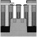
现在参见图1。提供半导体结构,所述半导体结构包括半导体基材(100),所述半导体基材包括Si半导体鳍片形式的半导体有源区域(200)。半导体有源区域(200)包括限定在外延生长的源极/漏极区(220/230)之间的通道区(210)。半导体有源区(200)通过SiO2浅沟槽隔离层(240;STI)彼此隔开。半导体结构还包括:在半导体基材(100)上的一组线结构(300),所述线结构(300)包括由SixNy无氧电介质栅极塞(320)封盖的栅极结构(310)、以及对栅极结构(310)和栅极塞(320)进行衬砌的SixNy无氧电介质间隔(330)。任选地,线结构(300)还可以包括覆盖(例如,衬砌)无氧电介质间隔(330)的SiN蚀刻停止衬层(未显示)。栅极结构(310)包括高k HfO2栅极电解质(311)、功函数调整金属(311)和W栅极接触部(312)。功函数调整金属可以选自:例如,TiN、TiN/TaN/TiN和TiN/TiAl/TaN/TiN。栅极结构(310)的纵向反向(平行于基材的最长尺寸)通常垂直于半导体鳍片(210)的纵向方向进行取向。用SiO2含氧介电材料(410)填充线结构(300)之间的沟槽(400),例如在源极/漏极区(220/230)之上的沟槽(400)。See Figure 1 now. A semiconductor structure is provided that includes a semiconductor substrate (100) including a semiconductor active region (200) in the form of a Si semiconductor fin. The semiconductor active region (200) includes a channel region (210) defined between epitaxially grown source/drain regions (220/230). The semiconductor active regions (200) are separated from each other bySiO2 shallow trench isolation layers (240; STI). The semiconductor structure also includes a set of line structures (300) on the semiconductor substrate (100), the line structures (300) including gate structures capped by aSix N yoxygen -free dielectric gate plug (320) (310), and aSix Nyoxygen -free dielectric spacer (330) lining the gate structure (310) and gate plug (320). Optionally, the line structure (300) may also include a SiN etch stop liner (not shown) overlying (eg, lining) the oxygen-free dielectric spacer (330). The gate structure (310) includes a high-kHfO2 gate electrolyte (311), a work function adjusting metal (311), and a W gate contact (312). The work function adjusting metal may be selected from, for example, TiN, TiN/TaN/TiN, and TiN/TiAl/TaN/TiN. The longitudinal inversion (parallel to the longest dimension of the substrate) of the gate structures (310) is generally oriented perpendicular to the longitudinal direction of the semiconductor fins (210). The trenches (400) between the line structures (300), eg, the trenches (400) over the source/drain regions (220/230), are filled withSiO2 oxygen-containing dielectric material (410).
我们现在参见图2。在半导体结构上沉积10nm的SiO2电介质覆盖层(500),并且在覆盖层(500)上提供图案化的SixNy无氧电介质硬掩模(600)。为了使得硬掩模(600)图案化,例如可以使用重叠的SiOC/高级图案化膜(APF)堆叠体或旋涂碳(SoC)/旋涂玻璃(SoG)堆叠体以及抗蚀剂层(未显示)。We now refer to Figure 2. A 10 nmSiO2 dielectric capping layer (500) is deposited on the semiconductor structure, and a patternedSixNy oxygen-free dielectric hardmask( 600) is provided on the capping layer (500). To pattern the hardmask (600), for example, an overlapping SiOC/Advanced Patterned Film (APF) stack or a spin-on-carbon (SoC)/spin-on-glass (SoG) stack and a resist layer (not shown) can be used show).
现在参见图3。通过相对于无氧介电材料[即,栅极塞(320)、间隔(330)和/或硬掩模(600)]选择性去除含氧介电材料[即,部分覆盖层(500)和/或经填充的沟槽(410)]来进行部分地向下蚀刻,达到使栅极塞(320)和间隔(330)的顶表面暴露的程度。例如,这可以使用基于C4F6/O2/Ar气体混合物的沉积和蚀刻步骤的循环过程,通过等离子体蚀刻来实现。可以使用15mT压力,100w RF 2MHz和100RF 27MHz电源以及110℃的卡盘温度。随后,可以执行湿清洁步骤以去除等离子体蚀刻之后任意剩余的残留物。See now Figure 3. By selectively removing the oxygen-containing dielectric material [ie, portions of the capping layer (500) and and/or filled trenches (410)] to partially etch down to the extent that the top surfaces of the gate plugs (320) and spacers (330) are exposed. For example, this can be achieved by plasma etching using a cyclic process basedon deposition and etching steps of aC4F6 /O2 /Ar gas mixture. 15mT pressure, 100w RF 2MHz and 100RF 27MHz power supply and 110°C chuck temperature can be used. Subsequently, a wet cleaning step can be performed to remove any residue remaining after the plasma etch.
我们现在参见图4。使TaSix层(700)相对于含氧介电材料(410)选择性沉积于无氧介电材料(320、330、600)上,由此形成覆盖栅极塞(320)、间隔(330)和/或硬掩模(600)的至少部分顶表面的掩模(700)。We now refer to Figure 4. A TaSix layer (700) is selectively deposited on the oxygen-free dielectric material (320, 330, 600) relative to the oxygen-containing dielectric material (410), thereby forming overlying gate plugs (320), spacers (330) and /or mask (700) of at least part of the top surface of hardmask (600).
我们现在参见图5。相对于TaSix(700)和无氧介电材料(320、330、600),进一步选择性地去除沟槽(400)中的含氧介电材料(410)。蚀刻使得其具有各向异性性质以及相对于TaSix(700)的极高选择性,使得TaSix材料(700)保护无氧介电材料(320、330、600)免于经受向下蚀刻。以此方式,可以完全去除含氧介电材料(410),而不会过度蚀刻到无氧介电材料(320、330)中。为实现这一点,基于C4F6/O2/Ar气体混合物,可以使用与图3所述相同的等离子体蚀刻。We now refer to Figure 5. The oxygen-containing dielectric material (410) in the trench (400) is further selectively removed relative to theTaSix (700) and the oxygen-free dielectric material (320, 330, 600). The etching gives it anisotropic properties and a very high selectivity relative toTaSix (700) so that theTaSix material (700) protects the oxygen-free dielectric material (320, 330, 600) from being etched down. In this way, the oxygen-containing dielectric material (410) can be completely removed without over-etching into the oxygen-free dielectric material (320, 330). To achieve this, the same plasma etch as described in FIG. 3 can be used, based on a C4 F6 /O2 /Ar gas mixture.
我们现在参见图6。使用ALD,用Ti和/或TiN屏障层(未显示)衬砌沟槽(400),并且使用CVD或ALD用W接触金属(810)过量填充。We now refer to Figure 6. Trench (400) is lined with a Ti and/or TiN barrier layer (not shown) using ALD and overfilled with W contact metal (810) using CVD or ALD.
我们现在参见图7。通过化学机械平面化(CMP)来去除接触金属(810)覆盖物,因此还同时去除TaSix材料(700)We now refer to Figure 7. The contact metal (810) cover is removed by chemical mechanical planarization (CMP), thus also removing the TaSix material (700) at the same time
在上文所呈现的实施例中,所用硬掩模(600)包含无氧介电材料,所述无氧介电材料通过选择性沉积TaSix通过TaSix材料(700)进行进一步强化。然而,显然硬掩模同样可以由对后续蚀刻技术具有足够抗蚀性的另一材料制成;因此,通过TaSix材料(700)进行强化是可选择的特征。In the embodiments presented above, the hard mask (600) used comprises an oxygen-free dielectric material that is further enhanced by theTaSix material (700) by selectively depositingTaSix . However, it is clear that the hard mask can also be made of another material that is sufficiently resistant to subsequent etching techniques; therefore, strengthening by theTaSix material (700) is an optional feature.
应理解,虽然本文已对本发明装置的优选实施方式、特定构造和构型以及材料进行了讨论,可对形式和细节进行各种改变或修改,而不背离本发明的范围和技术教导。例如,上面给出的任何方案仅仅代表可以使用的过程。可以从框图中添加或删除功能,并且可以在功能块之间交换操作。可以对所述方法增加或减少步骤而不背离本发明的范围。It will be understood that although preferred embodiments, specific constructions and configurations, and materials of the devices of the invention have been discussed herein, various changes or modifications in form and detail may be made without departing from the scope and technical teachings of the invention. For example, any schemes given above are merely representative of procedures that can be used. Functionality can be added or removed from the block diagram, and operations can be exchanged between functional blocks. Steps may be added or removed from the method without departing from the scope of the present invention.
Claims (20)
Translated fromChineseApplications Claiming Priority (2)
| Application Number | Priority Date | Filing Date | Title |
|---|---|---|---|
| EP18173024.3 | 2018-05-17 | ||
| EP18173024.3AEP3570317A1 (en) | 2018-05-17 | 2018-05-17 | Area-selective deposition of a mask material |
Publications (2)
| Publication Number | Publication Date |
|---|---|
| CN110504162A CN110504162A (en) | 2019-11-26 |
| CN110504162Btrue CN110504162B (en) | 2022-04-12 |
Family
ID=62200316
Family Applications (1)
| Application Number | Title | Priority Date | Filing Date |
|---|---|---|---|
| CN201910409763.4AActiveCN110504162B (en) | 2018-05-17 | 2019-05-16 | Area Selective Deposition of Masking Materials |
Country Status (3)
| Country | Link |
|---|---|
| US (1) | US10784158B2 (en) |
| EP (1) | EP3570317A1 (en) |
| CN (1) | CN110504162B (en) |
Families Citing this family (4)
| Publication number | Priority date | Publication date | Assignee | Title |
|---|---|---|---|---|
| US10892338B2 (en) | 2018-10-24 | 2021-01-12 | Globalfoundries Inc. | Scaled gate contact and source/drain cap |
| US11690216B2 (en)* | 2019-12-13 | 2023-06-27 | Micron Technology, Inc. | Structure to reduce bending in semiconductor devices |
| US11749753B2 (en)* | 2020-06-15 | 2023-09-05 | Taiwan Semiconductor Manufacturing Company Limited | Methods of forming a semiconductor device with a gate structure having a dielectric protection layer |
| EP3968387A1 (en) | 2020-09-15 | 2022-03-16 | Imec VZW | Gate spacer patterning |
Citations (3)
| Publication number | Priority date | Publication date | Assignee | Title |
|---|---|---|---|---|
| US4912543A (en)* | 1983-07-20 | 1990-03-27 | Siemens Aktiengesellschaft | Integrated semiconductor circuit having an external contacting track level consisting of aluminum or of an aluminum alloy |
| US5160407A (en)* | 1991-01-02 | 1992-11-03 | Applied Materials, Inc. | Low pressure anisotropic etch process for tantalum silicide or titanium silicide layer formed over polysilicon layer deposited on silicon oxide layer on semiconductor wafer |
| CN106952870A (en)* | 2016-01-07 | 2017-07-14 | 台湾积体电路制造股份有限公司 | Semiconductor device structure and method of forming the same |
Family Cites Families (14)
| Publication number | Priority date | Publication date | Assignee | Title |
|---|---|---|---|---|
| DE69029046T2 (en)* | 1989-03-16 | 1997-03-06 | Sgs Thomson Microelectronics | Contacts for semiconductor devices |
| US6025255A (en) | 1998-06-25 | 2000-02-15 | Vanguard International Semiconductor Corporation | Two-step etching process for forming self-aligned contacts |
| US6569778B2 (en) | 2001-06-28 | 2003-05-27 | Hynix Semiconductor Inc. | Method for forming fine pattern in semiconductor device |
| KR100426811B1 (en) | 2001-07-12 | 2004-04-08 | 삼성전자주식회사 | Semiconductor device having SAC and Fabrication Method thereof |
| US6716766B2 (en) | 2002-08-22 | 2004-04-06 | Micron Technology, Inc. | Process variation resistant self aligned contact etch |
| US7723229B2 (en) | 2005-04-22 | 2010-05-25 | Macronix International Co., Ltd. | Process of forming a self-aligned contact in a semiconductor device |
| US7682986B2 (en) | 2007-02-05 | 2010-03-23 | Lam Research Corporation | Ultra-high aspect ratio dielectric etch |
| US8487397B2 (en) | 2011-04-25 | 2013-07-16 | Nanya Technology Corporation | Method for forming self-aligned contact |
| US9530666B2 (en) | 2012-09-18 | 2016-12-27 | Tokyo Electron Limited | Plasma etching method and plasma etching apparatus |
| US9105700B2 (en) | 2013-12-12 | 2015-08-11 | Lam Research Corporation | Method for forming self-aligned contacts/vias with high corner selectivity |
| US9576811B2 (en) | 2015-01-12 | 2017-02-21 | Lam Research Corporation | Integrating atomic scale processes: ALD (atomic layer deposition) and ALE (atomic layer etch) |
| US10840105B2 (en)* | 2015-06-15 | 2020-11-17 | Taiwan Semiconductor Manufacturing Co., Ltd. | Gate structure with insulating structure and method for manufacturing the same |
| US9773700B1 (en)* | 2016-06-08 | 2017-09-26 | International Business Machines Corporation | Aligning conductive vias with trenches |
| US11508827B2 (en)* | 2018-09-26 | 2022-11-22 | Taiwan Semiconductor Manufacturing Co., Ltd. | Air spacer for a gate structure of a transistor |
- 2018
- 2018-05-17EPEP18173024.3Apatent/EP3570317A1/ennot_activeWithdrawn
- 2019
- 2019-05-15USUS16/412,923patent/US10784158B2/enactiveActive
- 2019-05-16CNCN201910409763.4Apatent/CN110504162B/enactiveActive
Patent Citations (3)
| Publication number | Priority date | Publication date | Assignee | Title |
|---|---|---|---|---|
| US4912543A (en)* | 1983-07-20 | 1990-03-27 | Siemens Aktiengesellschaft | Integrated semiconductor circuit having an external contacting track level consisting of aluminum or of an aluminum alloy |
| US5160407A (en)* | 1991-01-02 | 1992-11-03 | Applied Materials, Inc. | Low pressure anisotropic etch process for tantalum silicide or titanium silicide layer formed over polysilicon layer deposited on silicon oxide layer on semiconductor wafer |
| CN106952870A (en)* | 2016-01-07 | 2017-07-14 | 台湾积体电路制造股份有限公司 | Semiconductor device structure and method of forming the same |
Also Published As
| Publication number | Publication date |
|---|---|
| CN110504162A (en) | 2019-11-26 |
| US20190355619A1 (en) | 2019-11-21 |
| US10784158B2 (en) | 2020-09-22 |
| EP3570317A1 (en) | 2019-11-20 |
Similar Documents
| Publication | Publication Date | Title |
|---|---|---|
| CN108933084B (en) | Replacement metal gate patterning for nanosheet devices | |
| TWI508192B (en) | Integrated circuit with replacement gate structure and manufacturing method thereof | |
| CN111490092B (en) | Semiconductor structures and methods of forming them | |
| TWI643252B (en) | Method of forming a semiconductor device | |
| TWI518755B (en) | Integrated circuit structure and manufacturing method thereof | |
| US20130307079A1 (en) | Etch resistant barrier for replacement gate integration | |
| KR101951088B1 (en) | Self-aligned metal gate etch back process and device | |
| CN110504162B (en) | Area Selective Deposition of Masking Materials | |
| CN111128887B (en) | Method of forming a semiconductor device | |
| CN109390235B (en) | Semiconductor structure and forming method thereof | |
| CN106952874A (en) | Formation method of multi-threshold voltage fin transistor | |
| TW202131389A (en) | Semiconductor structure and method forming the same | |
| CN110571193A (en) | Method for manufacturing single diffusion barrier structure and method for manufacturing semiconductor device | |
| TW202107705A (en) | Semiconductor structure and forming method thereof | |
| KR20250003381A (en) | Semiconductor device and method | |
| CN111863723A (en) | Semiconductor structure and method of forming the same | |
| US20250273473A1 (en) | Semiconductor FinFET Device and Method | |
| US20200402807A1 (en) | Semiconductor FinFET Device and Method | |
| CN111613581B (en) | Semiconductor structure and forming method thereof | |
| CN105762187B (en) | Semiconductor device and method for manufacturing the same | |
| CN113903666B (en) | Semiconductor structure and method of forming the same | |
| CN106952815A (en) | Method for forming fin transistors | |
| CN109103102B (en) | Semiconductor structure and method of forming the same | |
| TW202501718A (en) | Semiconductor structure | |
| TWI811783B (en) | Method for forming semiconductor structure |
Legal Events
| Date | Code | Title | Description |
|---|---|---|---|
| PB01 | Publication | ||
| PB01 | Publication | ||
| SE01 | Entry into force of request for substantive examination | ||
| SE01 | Entry into force of request for substantive examination | ||
| GR01 | Patent grant | ||
| GR01 | Patent grant |