CN110471568B - Touch structure, touch display device and preparation method of touch display device - Google Patents
Touch structure, touch display device and preparation method of touch display deviceDownload PDFInfo
- Publication number
- CN110471568B CN110471568BCN201910755780.3ACN201910755780ACN110471568BCN 110471568 BCN110471568 BCN 110471568BCN 201910755780 ACN201910755780 ACN 201910755780ACN 110471568 BCN110471568 BCN 110471568B
- Authority
- CN
- China
- Prior art keywords
- touch
- electrodes
- electrode
- sub
- dummy
- Prior art date
- Legal status (The legal status is an assumption and is not a legal conclusion. Google has not performed a legal analysis and makes no representation as to the accuracy of the status listed.)
- Active
Links
Images


Classifications
- G—PHYSICS
- G06—COMPUTING OR CALCULATING; COUNTING
- G06F—ELECTRIC DIGITAL DATA PROCESSING
- G06F3/00—Input arrangements for transferring data to be processed into a form capable of being handled by the computer; Output arrangements for transferring data from processing unit to output unit, e.g. interface arrangements
- G06F3/01—Input arrangements or combined input and output arrangements for interaction between user and computer
- G06F3/03—Arrangements for converting the position or the displacement of a member into a coded form
- G06F3/041—Digitisers, e.g. for touch screens or touch pads, characterised by the transducing means
- G06F3/044—Digitisers, e.g. for touch screens or touch pads, characterised by the transducing means by capacitive means
- G06F3/0443—Digitisers, e.g. for touch screens or touch pads, characterised by the transducing means by capacitive means using a single layer of sensing electrodes
- G—PHYSICS
- G02—OPTICS
- G02F—OPTICAL DEVICES OR ARRANGEMENTS FOR THE CONTROL OF LIGHT BY MODIFICATION OF THE OPTICAL PROPERTIES OF THE MEDIA OF THE ELEMENTS INVOLVED THEREIN; NON-LINEAR OPTICS; FREQUENCY-CHANGING OF LIGHT; OPTICAL LOGIC ELEMENTS; OPTICAL ANALOGUE/DIGITAL CONVERTERS
- G02F1/00—Devices or arrangements for the control of the intensity, colour, phase, polarisation or direction of light arriving from an independent light source, e.g. switching, gating or modulating; Non-linear optics
- G02F1/01—Devices or arrangements for the control of the intensity, colour, phase, polarisation or direction of light arriving from an independent light source, e.g. switching, gating or modulating; Non-linear optics for the control of the intensity, phase, polarisation or colour
- G02F1/13—Devices or arrangements for the control of the intensity, colour, phase, polarisation or direction of light arriving from an independent light source, e.g. switching, gating or modulating; Non-linear optics for the control of the intensity, phase, polarisation or colour based on liquid crystals, e.g. single liquid crystal display cells
- G02F1/133—Constructional arrangements; Operation of liquid crystal cells; Circuit arrangements
- G02F1/1333—Constructional arrangements; Manufacturing methods
- G02F1/13338—Input devices, e.g. touch panels
- G—PHYSICS
- G06—COMPUTING OR CALCULATING; COUNTING
- G06F—ELECTRIC DIGITAL DATA PROCESSING
- G06F3/00—Input arrangements for transferring data to be processed into a form capable of being handled by the computer; Output arrangements for transferring data from processing unit to output unit, e.g. interface arrangements
- G06F3/01—Input arrangements or combined input and output arrangements for interaction between user and computer
- G06F3/03—Arrangements for converting the position or the displacement of a member into a coded form
- G06F3/041—Digitisers, e.g. for touch screens or touch pads, characterised by the transducing means
- G06F3/0412—Digitisers structurally integrated in a display
- G—PHYSICS
- G06—COMPUTING OR CALCULATING; COUNTING
- G06F—ELECTRIC DIGITAL DATA PROCESSING
- G06F3/00—Input arrangements for transferring data to be processed into a form capable of being handled by the computer; Output arrangements for transferring data from processing unit to output unit, e.g. interface arrangements
- G06F3/01—Input arrangements or combined input and output arrangements for interaction between user and computer
- G06F3/03—Arrangements for converting the position or the displacement of a member into a coded form
- G06F3/041—Digitisers, e.g. for touch screens or touch pads, characterised by the transducing means
- G06F3/044—Digitisers, e.g. for touch screens or touch pads, characterised by the transducing means by capacitive means
- G06F3/0446—Digitisers, e.g. for touch screens or touch pads, characterised by the transducing means by capacitive means using a grid-like structure of electrodes in at least two directions, e.g. using row and column electrodes
- G—PHYSICS
- G06—COMPUTING OR CALCULATING; COUNTING
- G06F—ELECTRIC DIGITAL DATA PROCESSING
- G06F2203/00—Indexing scheme relating to G06F3/00 - G06F3/048
- G06F2203/041—Indexing scheme relating to G06F3/041 - G06F3/045
- G06F2203/04103—Manufacturing, i.e. details related to manufacturing processes specially suited for touch sensitive devices
- G—PHYSICS
- G06—COMPUTING OR CALCULATING; COUNTING
- G06F—ELECTRIC DIGITAL DATA PROCESSING
- G06F2203/00—Indexing scheme relating to G06F3/00 - G06F3/048
- G06F2203/041—Indexing scheme relating to G06F3/041 - G06F3/045
- G06F2203/04111—Cross over in capacitive digitiser, i.e. details of structures for connecting electrodes of the sensing pattern where the connections cross each other, e.g. bridge structures comprising an insulating layer, or vias through substrate
- G—PHYSICS
- G06—COMPUTING OR CALCULATING; COUNTING
- G06F—ELECTRIC DIGITAL DATA PROCESSING
- G06F2203/00—Indexing scheme relating to G06F3/00 - G06F3/048
- G06F2203/041—Indexing scheme relating to G06F3/041 - G06F3/045
- G06F2203/04112—Electrode mesh in capacitive digitiser: electrode for touch sensing is formed of a mesh of very fine, normally metallic, interconnected lines that are almost invisible to see. This provides a quite large but transparent electrode surface, without need for ITO or similar transparent conductive material
Landscapes
- Engineering & Computer Science (AREA)
- General Engineering & Computer Science (AREA)
- Theoretical Computer Science (AREA)
- Physics & Mathematics (AREA)
- General Physics & Mathematics (AREA)
- Human Computer Interaction (AREA)
- Nonlinear Science (AREA)
- Chemical & Material Sciences (AREA)
- Crystallography & Structural Chemistry (AREA)
- Mathematical Physics (AREA)
- Optics & Photonics (AREA)
- Position Input By Displaying (AREA)
- Devices For Indicating Variable Information By Combining Individual Elements (AREA)
Abstract
Translated fromChinese
Description
Translated fromChinese技术领域technical field
本发明涉及显示领域,尤其涉及一种触控结构、触控显示装置及其制备方法。The present invention relates to the field of display, in particular to a touch structure, a touch display device and a preparation method thereof.
背景技术Background technique
随着显示技术的发展,触控屏(Touch Panel)技术进入快速发展的时期。电容式触控屏具有定位精确灵敏、触摸手感好以及使用寿命长等特点,越来越多的受到关注由于互容式触控屏可以实现多点触控,因而互容式触控屏成为目前触控屏市场上的主流和未来的发展趋势。With the development of display technology, touch panel (Touch Panel) technology has entered a period of rapid development. Capacitive touch screen has the characteristics of precise and sensitive positioning, good touch feeling and long service life, and more and more attention has been paid to it. Because mutual capacitive touch screen can realize multi-touch, mutual capacitive touch screen has become the current The mainstream and future development trends in the touch screen market.
发明内容Contents of the invention
本发明的实施例提供一种触控结构、触控显示装置及其制备方法,可以增加触控结构的折叠和卷曲性,提高其可靠性。Embodiments of the present invention provide a touch structure, a touch display device and a manufacturing method thereof, which can increase the folding and curling properties of the touch structure and improve its reliability.
为达到上述目的,本发明的实施例采用如下技术方案:In order to achieve the above object, embodiments of the present invention adopt the following technical solutions:
一方面,提供了一种触控结构,包括:多个间隔设置的第一触控电极以及多个间隔设置的第二触控电极,所述第一触控电极和所述第二触控电极交叉且相互绝缘。In one aspect, a touch control structure is provided, including: a plurality of first touch electrodes arranged at intervals and a plurality of second touch electrodes arranged at intervals, the first touch electrodes and the second touch electrodes crossed and insulated from each other.
所述第一触控电极包括多个直接连接的第一触控子电极,所述第二触控电极包括多个第二触控子电极,且任意相邻所述第二触控子电极通过搭桥电连接;所述第二触控子电极与所述搭桥分设于绝缘层沿厚度方向的两侧,所述第二触控子电极与所述第一触控子电极位于所述绝缘层同侧。The first touch electrode includes a plurality of directly connected first touch sub-electrodes, the second touch electrode includes a plurality of second touch sub-electrodes, and any adjacent second touch sub-electrodes pass through The bridge is electrically connected; the second touch sub-electrode and the bridge are separately arranged on both sides of the insulating layer along the thickness direction, and the second touch sub-electrode and the first touch sub-electrode are located on the same side of the insulating layer side.
所述触控结构还包括虚拟电极,所述虚拟电极与所述第一触控电极和所述第二触控电极均绝缘;所述虚拟电极用于消影。所述虚拟电极与所述搭桥设置于所述绝缘层的同一侧。The touch control structure further includes a dummy electrode, which is insulated from both the first touch electrode and the second touch electrode; the dummy electrode is used for shadow removal. The dummy electrode and the bridge are disposed on the same side of the insulating layer.
可选的,所述虚拟电极与所述搭桥的同层同材料。Optionally, the dummy electrode is made of the same material as the same layer of the bridge.
可选的,所述第一触控电极与所述第二触控子电极同层同材料。Optionally, the first touch electrode and the second touch sub-electrode have the same layer and the same material.
可选的,所述虚拟电极设置于所述第一触控电极和所述第二触控电极之间的区域。Optionally, the dummy electrode is disposed in a region between the first touch electrode and the second touch electrode.
可选的,所述第一触控子电极和所述第二触控子电极均包括至少一个第一镂空区。Optionally, both the first touch sub-electrode and the second touch sub-electrode include at least one first hollow area.
所述虚拟电极包括多个虚拟子电极,所述虚拟子电极与所述第一镂空区一一对应;沿所述绝缘层的厚度方向,一一对应的所述第一镂空区的正投影覆盖所述虚拟子电极的正投影。The dummy electrode includes a plurality of dummy sub-electrodes, and the dummy sub-electrodes are in one-to-one correspondence with the first hollowed-out area; along the thickness direction of the insulating layer, the orthographic projection of the one-to-one corresponding first hollowed-out area covers The orthographic projection of the virtual sub-electrodes.
可选的,所述第一触控电极和所述第二触控子电极、所述搭桥、所述虚拟电极的材料均选自透明金属氧化物、金属、导电无机物或者导电有机物中的一种。Optionally, materials of the first touch electrode and the second touch sub-electrode, the bridge, and the dummy electrode are all selected from one of transparent metal oxides, metals, conductive inorganic substances or conductive organic substances. kind.
可选的,所述第一触控子电极和所述第二触控子电极均呈网格结构,且所述第一触控电极和所述第二触控电极的材料为金属单质或合金。Optionally, both the first touch sub-electrodes and the second touch sub-electrodes have a grid structure, and the materials of the first touch electrodes and the second touch electrodes are metal simple substances or alloys .
再一方面,提供一种触控基板,包括衬底、设置于所述衬底上的所述触控结构。In another aspect, a touch control substrate is provided, including a substrate and the touch control structure disposed on the substrate.
可选的,触控基板还包括设置于所述触控结构远离所述衬底一侧的保护层。Optionally, the touch control substrate further includes a protective layer disposed on a side of the touch control structure away from the substrate.
另一方面,提供一种触控显示装置,包括显示面板和所述触控结构。In another aspect, a touch display device is provided, including a display panel and the touch structure.
其中,在所述触控结构中的第一触控子电极和所述第二触控子电极包括第一镂空区的情况下,所述第一镂空区露出所述显示面板中亚像素的发光区。Wherein, in the case where the first touch sub-electrode and the second touch sub-electrode in the touch control structure include a first hollow area, the first hollow area exposes the light emission of the sub-pixels in the display panel. district.
可选的,所述显示装置还包括显示面板,所述触控结构设置于所述显示面板的出光侧。Optionally, the display device further includes a display panel, and the touch structure is disposed on a light-emitting side of the display panel.
再一方面,提供一种触控结构的制备方法,包括:In another aspect, a method for preparing a touch structure is provided, including:
通过一次构图工艺形成多个间隔的第一触控电极,所述第一触控电极包括沿第一方向排布且直接连接的多个第一触控子电极;并形成多排第二触控子电极,每排中的所述第二触控子电极沿第二方向排布,所述第二触控子电极与所述第一触控电极绝缘;所述第一方向和所述第二方向交叉。A plurality of spaced first touch electrodes are formed through a patterning process, and the first touch electrodes include a plurality of first touch sub-electrodes arranged along the first direction and directly connected; and multiple rows of second touch electrodes are formed. Sub-electrodes, the second touch sub-electrodes in each row are arranged along a second direction, and the second touch sub-electrodes are insulated from the first touch electrodes; the first direction and the second direction cross.
通过一次构图工艺形成绝缘层,所述绝缘层包括多个过孔。The insulating layer is formed through one patterning process, and the insulating layer includes a plurality of via holes.
通过一次构图工艺形成多个间隔的搭桥和虚拟电极,所述虚拟电极与所述搭桥绝缘;沿所述第二方向,任意相邻所述第二触控子电极分别通过一个所述过孔与同一所述搭桥电连接,其中,每排中多个所述第二触控子电极以及电连接的多个所述搭桥构成一个第二触控电极;所述虚拟电极用于消影。A plurality of spaced bridges and dummy electrodes are formed through a single patterning process, and the dummy electrodes are insulated from the bridges; along the second direction, any adjacent second touch sub-electrodes are respectively connected to each other through one of the via holes. The same bridge is electrically connected, wherein a plurality of the second touch sub-electrodes in each row and a plurality of the electrically connected bridges form a second touch electrode; the dummy electrode is used for shadow removal.
又一方面,提供一种触控结构的制备方法,包括:In yet another aspect, a method for preparing a touch structure is provided, including:
通过一次构图工艺形成多个间隔的搭桥和虚拟电极,所述虚拟电极与所述搭桥绝缘;所述虚拟电极用于消影。A plurality of spaced bridges and dummy electrodes are formed through one patterning process, and the dummy electrodes are insulated from the bridges; the dummy electrodes are used for shadow elimination.
通过一次构图工艺形成绝缘层,所述绝缘层包括多个过孔。The insulating layer is formed through one patterning process, and the insulating layer includes a plurality of via holes.
通过一次构图工艺形成多个间隔的第一触控电极,所述第一触控电极包括沿第一方向排布且直接连接的多个第一触控子电极;并形成多排第二触控子电极,所述第二触控子电极与所述第一触控电极绝缘;每排中的所述第二触控子电极沿第二方向排布,且每排中任意相邻所述第二触控子电极分别通过一个所述过孔与同一所述搭桥电连接;其中,每排中多个所述第二触控子电极以及电连接的多个所述搭桥构成一个第二触控电极;所述第一方向和所述第二方向交叉。A plurality of spaced first touch electrodes are formed through a patterning process, and the first touch electrodes include a plurality of first touch sub-electrodes arranged along the first direction and directly connected; and multiple rows of second touch electrodes are formed. Sub-electrodes, the second touch sub-electrodes are insulated from the first touch electrodes; the second touch sub-electrodes in each row are arranged along the second direction, and any adjacent to the first touch electrodes in each row The two touch sub-electrodes are respectively electrically connected to the same bridge through one of the via holes; wherein, a plurality of the second touch sub-electrodes in each row and a plurality of the electrically connected bridges constitute a second touch electrodes; the first direction and the second direction intersect.
本发明的实施例提供一种触控结构、触控显示装置及其制备方法,在触控结构中,通过将第二触控子电极与搭桥分设于绝缘层沿厚度方向的两侧,再将第二触控子电极与第一触控子电极设置于绝缘层同侧,虚拟电极与搭桥设置于绝缘层的同一侧,即,使第一触控子电极和第二触控子电极,与虚拟电极位于绝缘层的不同侧,在保证消影的前提下,可以增加折叠和卷曲性能。此外,这样的设计还能够平衡绝缘层沿厚度方向的两侧受到的应力,降低触控结构出现断裂脱落等问题的风险,从而提高了触控结构的可靠性。Embodiments of the present invention provide a touch control structure, a touch display device and a manufacturing method thereof. In the touch control structure, the second touch sub-electrode and the bridge are separately arranged on both sides of the insulating layer along the thickness direction, and then the The second touch sub-electrode and the first touch sub-electrode are arranged on the same side of the insulating layer, and the dummy electrode and the bridge are arranged on the same side of the insulating layer, that is, the first touch sub-electrode and the second touch sub-electrode are connected to the same side of the insulating layer. The dummy electrodes are located on different sides of the insulating layer, which can increase the folding and curling performance under the premise of ensuring shadow elimination. In addition, such a design can also balance the stress on both sides of the insulating layer along the thickness direction, reducing the risk of problems such as breakage and falling off of the touch structure, thereby improving the reliability of the touch structure.
附图说明Description of drawings
为了更清楚地说明本发明实施例或现有技术中的技术方案,下面将对实施例或现有技术描述中所需要使用的附图作简单地介绍,显而易见地,下面描述中的附图仅仅是本发明的一些实施例,对于本领域普通技术人员来讲,在不付出创造性劳动的前提下,还可以根据这些附图获得其他的附图。In order to more clearly illustrate the technical solutions in the embodiments of the present invention or the prior art, the following will briefly introduce the drawings that need to be used in the description of the embodiments or the prior art. Obviously, the accompanying drawings in the following description are only These are some embodiments of the present invention. Those skilled in the art can also obtain other drawings based on these drawings without creative work.
图1a为本发明实施例提供的一种触控显示装置的结构示意图;Fig. 1a is a schematic structural diagram of a touch display device provided by an embodiment of the present invention;
图1b为本发明实施例提供的再一种触控显示装置的结构示意图;Fig. 1b is a schematic structural diagram of another touch display device provided by an embodiment of the present invention;
图1c为本发明实施例提供的另一种触控显示装置的结构示意图;Fig. 1c is a schematic structural diagram of another touch display device provided by an embodiment of the present invention;
图2a为本发明实施例提供的又一种触控显示装置的结构示意图;Fig. 2a is a schematic structural diagram of another touch display device provided by an embodiment of the present invention;
图2b为本发明实施例提供的又一种触控显示装置的结构示意图;Fig. 2b is a schematic structural diagram of another touch display device provided by an embodiment of the present invention;
图3a为相关技术提供的一种互容式触控结构的结构示意图;FIG. 3a is a schematic structural diagram of a mutual capacitive touch structure provided by the related art;
图3b为图3a中AA'向的剖面示意图;Fig. 3b is a schematic cross-sectional view of AA' direction in Fig. 3a;
图4a为本发明实施例提供的一种触控结构的结构示意图;FIG. 4a is a schematic structural diagram of a touch structure provided by an embodiment of the present invention;
图4b为本发明实施例图4a中BB'向的剖面示意图;Fig. 4b is a schematic cross-sectional view of BB' in Fig. 4a according to an embodiment of the present invention;
图5a为本发明实施例提供的再一种触控结构的结构示意图;Fig. 5a is a schematic structural diagram of another touch structure provided by an embodiment of the present invention;
图5b为本发明实施例图5a中CC'向的剖面示意图;Fig. 5b is a schematic cross-sectional view of CC' direction in Fig. 5a according to the embodiment of the present invention;
图6a为本发明实施例提供的另一种触控结构的结构示意图;FIG. 6a is a schematic structural diagram of another touch structure provided by an embodiment of the present invention;
图6b为本发明实施例图6a中DD'向的剖面示意图;Fig. 6b is a schematic cross-sectional view of DD' in Fig. 6a according to the embodiment of the present invention;
图7为本发明实施例提供的一种第一触控子电极的结构示意图;FIG. 7 is a schematic structural diagram of a first touch sub-electrode provided by an embodiment of the present invention;
图8为本发明实施例提供的一种触控基板的结构示意图;FIG. 8 is a schematic structural diagram of a touch substrate provided by an embodiment of the present invention;
图9为本发明实施例提供的一种触控结构的制备方法的流程示意图;FIG. 9 is a schematic flowchart of a method for manufacturing a touch structure provided by an embodiment of the present invention;
图10a-图10c为本发明实施例提供的一种形成触控结构的过程示意图;10a-10c are schematic diagrams of a process of forming a touch structure provided by an embodiment of the present invention;
图11为本发明实施例提供的又一种触控结构的制备方法的流程示意图。FIG. 11 is a schematic flowchart of another manufacturing method of a touch control structure provided by an embodiment of the present invention.
图12a-图12c为本发明实施例提供的又一种形成触控结构的过程示意图。12a-12c are schematic diagrams of another process for forming a touch structure provided by an embodiment of the present invention.
附图标记:Reference signs:
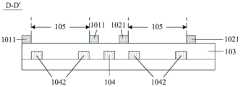
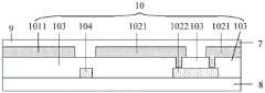
1-液晶显示面板;2-盖板玻璃;3-电致发光显示面板(光致发光显示面板);4-偏光片;5-第一光学胶;6-衬底;7-保护层;10-触控结构;11-阵列基板;12-对置基板;13-液晶层;14-上偏光片;15-下偏光片;31-显示用基板;32-封装层;101-第一触控电极;1011-第一触控子电极;102-第二触控电极;1021-第二触控子电极;1022-搭桥;103-绝缘层;104-虚拟电极;1042-虚拟子电极;1042a-第二镂空区域;105-第一镂空区域;110-第一衬底;111-薄膜晶体管;112-像素电极;113-公共电极;114-第一绝缘层;115-第二绝缘层;120-第二衬底;121-彩色滤光层;122-黑矩阵图案;310-第三衬底;311-阳极;312-发光功能层;313-阴极;314-像素界定层;315-平坦层。1-LCD display panel; 2-cover glass; 3-electroluminescence display panel (photoluminescence display panel); 4-polarizer; 5-first optical glue; 6-substrate; 7-protective layer; 10 -touch structure; 11-array substrate; 12-opposite substrate; 13-liquid crystal layer; 14-upper polarizer; 15-lower polarizer; 31-display substrate; 32-packaging layer; 101-first touch Electrode; 1011-first touch sub-electrode; 102-second touch electrode; 1021-second touch sub-electrode; 1022-bridge; 103-insulating layer; 104-dummy electrode; 1042-dummy sub-electrode; 105-first hollow area; 110-first substrate; 111-thin film transistor; 112-pixel electrode; 113-common electrode; 114-first insulating layer; 115-second insulating layer; 120- 121-color filter layer; 122-black matrix pattern; 310-third substrate; 311-anode; 312-light-emitting functional layer; 313-cathode; 314-pixel defining layer;
具体实施方式Detailed ways
下面将结合本发明实施例中的附图,对本发明实施例中的技术方案进行清楚、完整地描述,显然,所描述的实施例仅仅是本发明一部分实施例,而不是全部的实施例。基于本发明中的实施例,本领域普通技术人员在没有做出创造性劳动前提下所获得的所有其他实施例,都属于本发明保护的范围。The following will clearly and completely describe the technical solutions in the embodiments of the present invention with reference to the accompanying drawings in the embodiments of the present invention. Obviously, the described embodiments are only some, not all, embodiments of the present invention. Based on the embodiments of the present invention, all other embodiments obtained by persons of ordinary skill in the art without making creative efforts belong to the protection scope of the present invention.
本发明实施例提供一种触控显示装置,该触控显示装置可以为具有触控功能的液晶显示装置(Liquid Crystal Display,简称LCD),该触控显示装置也可以为具有触控功能的电致发光显示装置或光致发光显示装置。在触控显示装置为电致发光显示装置的情况下,电致发光显示装置可以为有机电致发光显示装置(Organic Light-Emitting Diode,简称OLED)或量子点电致发光显示装置(Quantum Dot Light Emitting Diodes,简称QLED)。在触控显示装置为光致发光显示装置的情况下,光致发光显示装置可以为量子点光致发光显示装置。An embodiment of the present invention provides a touch display device. The touch display device may be a Liquid Crystal Display (LCD for short) with a touch function, and the touch display device may also be an electronic device with a touch function. Luminescent display devices or photoluminescent display devices. In the case where the touch display device is an electroluminescent display device, the electroluminescent display device may be an organic electroluminescent display device (Organic Light-Emitting Diode, OLED for short) or a quantum dot electroluminescent display device (Quantum Dot Light Emitting Diodes, referred to as QLED). In the case that the touch display device is a photoluminescence display device, the photoluminescence display device may be a quantum dot photoluminescence display device.
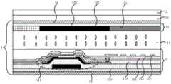
在触控显示装置为液晶显示装置的情况下,触控显示装置包括盖板玻璃、触控结构、液晶显示面板以及背光模组。背光模组用于为液晶显示面板提供光源。如图1a、图1b以及图1c所示,液晶显示面板1的主要结构包括阵列基板11、对置基板12以及设置在阵列基板11和对置基板12之间的液晶层13。When the touch display device is a liquid crystal display device, the touch display device includes a cover glass, a touch structure, a liquid crystal display panel and a backlight module. The backlight module is used to provide light source for the liquid crystal display panel. As shown in FIG. 1a , FIG. 1b and FIG. 1c , the main structure of the liquid crystal display panel 1 includes an array substrate 11 , an
如图1a、图1b以及图1c所示,阵列基板11包括第一衬底110、设置于第一衬底110上且位于每个亚像素中的薄膜晶体管111和像素电极112。薄膜晶体管111包括有源层、源极、漏极、栅极及栅绝缘层,源极和漏极分别与有源层接触,像素电极112与薄膜晶体管111的漏极电连接。As shown in FIG. 1 a , FIG. 1 b and FIG. 1 c , the array substrate 11 includes a
薄膜晶体管111可以是底栅型薄膜晶体管、顶栅型薄膜晶体管、双栅型薄膜晶体管中的一种,图1a、图1b以及图1c中均以底栅型薄膜晶体管为例进行示意。The
在一些实施例中,如图1a、图1b以及图1c所示,阵列基板11还包括设置于第一衬底110上的公共电极113。像素电极112和公共电极113可以设置在同一层,在此情况下,像素电极112和公共电极113均为包括多个条状子电极的梳齿结构。像素电极112和公共电极113也可以设置在不同层,在此情况下,如图1a、图1b以及图1c所示,像素电极112和公共电极113之间设置有第一绝缘层114。在公共电极113设置在薄膜晶体管111和像素电极112之间的情况下,如图1a、图1b以及图1c所示,公共电极113与薄膜晶体管111之间还设置有第二绝缘层115。In some embodiments, as shown in FIG. 1 a , FIG. 1 b and FIG. 1 c , the array substrate 11 further includes a
在另一些实施例中,公共电极113设置在对置基板12上。In other embodiments, the
如图1a、图1b以及图1c所示,对置基板12包括第二衬底120、设置于第二衬底120上的彩色滤光层121,在此情况下,对置基板12也可以称为彩膜基板(Color filter,简称CF)。彩色滤光层121至少包括第一颜色滤光单元、第二颜色滤光单元和第三颜色滤光单元,第一颜色滤光单元、第二颜色滤光单元和第三颜色滤光单元一一对应的位于一个亚像素中。其中,第一颜色、第二颜色和第三颜色为三基色,例如为红色、绿色和蓝色。对置基板12还包括设置在第二衬底120上的黑矩阵图案122,黑矩阵图案122用于将第一颜色滤光单元、第二颜色滤光单元和第三颜色滤光单元间隔开。As shown in FIG. 1a, FIG. 1b and FIG. 1c, the
如图1a、图1b以及图1c所示,液晶显示面板1还包括设置在对置基板12远离液晶层13一侧的上偏光片14以及设置在阵列基板11远离液晶层13一侧的下偏光片15。As shown in FIG. 1a, FIG. 1b and FIG. 1c, the liquid crystal display panel 1 further includes an
在一些实施例中,触控结构10设置在第一衬底110远离对置基板12的一侧,或者,设置在第二衬底120远离阵列基板11的一侧。In some embodiments, the
基于此,如图1a和图1b所示,触控结构10可以设置于液晶显示面板1的出光侧。其中,如图1a所示,触控结构10可以设置在盖板玻璃2和上偏光片14之间,在此基础上,触控结构10例如可设置在盖板玻璃2上。或者,如图1b所示,触控结构10可以设置在上偏光片14和对置基板12之间,在此基础上,触控结构10例如可设置在第二衬底120远离阵列基板11的表面。Based on this, as shown in FIG. 1 a and FIG. 1 b , the
在另一些实施例中,如图1c所示,触控结构10设置在第一衬底110和第二衬底120之间。In other embodiments, as shown in FIG. 1 c , the
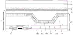
在触控显示装置为电致发光显示装置的情况下,如图2a和图2b所示,电致发光显示装置主要结构包括电致发光显示面板3、触控结构10、偏光片4、第一光学胶(OpticallyClear Adhesive,简称OCA)5和盖板玻璃2。When the touch display device is an electroluminescence display device, as shown in FIG. 2a and FIG. 2b, the main structure of the electroluminescence display device includes an
其中,电致发光显示面板3包括显示用基板31和用于封装显示用基板31的封装层32。此处,封装层32可以为封装薄膜,也可以为封装基板。Wherein, the
如图2a和图2b所示,上述的显示用基板31包括第三衬底310、设置在第三衬底310上且位于每个亚像素中的发光器件和驱动电路。驱动电路包括多个薄膜晶体管,且其中一个薄膜晶体管111为驱动晶体管。发光器件包括阳极311、发光功能层312以及阴极313,阳极311和驱动晶体管111的漏极电连接。显示用基板31还包括像素界定层314,像素界定层314包括多个开口区,每个发光器件一一对应的设置在一个开口区中。As shown in FIG. 2 a and FIG. 2 b , the above-mentioned
发光器件可以是底发光型发光器件、顶发光型发光器件以及双面发光型发光器件中的一种。The light emitting device may be one of a bottom emission type light emitting device, a top emission type light emitting device, and a double side emission type light emitting device.
在一些实施例中,发光功能层312包括发光层。在另一些实施例中,发光功能层312除包括发光层外,还包括电子传输层(election transporting layer,简称ETL)、电子注入层(election injection layer,简称EIL)、空穴传输层(hole transporting layer,简称HTL)以及空穴注入层(hole injection layer,简称HIL)中的一层或多层。In some embodiments, the light emitting
如图2a所示,显示用基板31还包括设置在驱动晶体管和阳极311之间的平坦层315。As shown in FIG. 2 a , the
在一些实施例中,触控结构10可以设置于电致发光显示面板3的出光侧。其中,如图2a所示,触控结构10可直接设置在封装层32上,即,触控结构10和封装层32之间不设置其它膜层。或者,如图2b所示,触控结构10可以设置在盖板玻璃2与偏光片4之间。示例的,触控结构10设置在盖板玻璃2上。In some embodiments, the
对于光致发光显示装置,其结构与电致发光显示装置类似,参考上述电致发光显示装置的结构即可,在此不再赘述。As for the photoluminescent display device, its structure is similar to that of the electroluminescent display device, and it is sufficient to refer to the structure of the above electroluminescent display device, and details will not be repeated here.
在触控显示装置为电致发光显示装置或光致发光显示装置的情况下,触控显示装置更容易制作成柔性显示装置。In the case that the touch display device is an electroluminescence display device or a photoluminescence display device, the touch display device is more easily fabricated into a flexible display device.
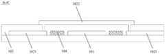
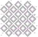
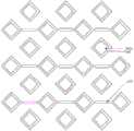
如图4a-图4b、图5a-图5b以及图6a-图6b所示,本发明实施例提供一种触控结构10,包括:多个间隔设置的第一触控电极101以及多个间隔设置的第二触控电极102,第一触控电极101和第二触控电极102交叉且相互绝缘。As shown in Fig. 4a-Fig. 4b, Fig. 5a-Fig. 5b and Fig. 6a-Fig. The
第一触控电极101包括多个直接连接的第一触控子电极1011,第二触控电极102包括多个第二触控子电极1021,且任意相邻所述第二触控子电极1021通过搭桥1022电连接;第二触控子电极1021与搭桥1022分设于绝缘层103沿厚度方向的两侧,第二触控子电极1021与第一触控子电极1011位于绝缘层103同侧。The
触控结构10还包括虚拟电极104,虚拟电极104与第一触控电极101和第二触控电极102均绝缘;虚拟电极104用于消影。虚拟电极104与搭桥1022设置于绝缘层103的同一侧。The
由上述对触控结构10的描述可知,该触控结构10为互容式触控结构,其实现触控的原理为:在第一触控电极101和第二触控电极102交叉的地方会形成电容,即,在交叉的地方第一触控电极101和第二触控电极102分别构成了电容的电极。当手指触摸到触控结构10时,影响了触摸点附近第一触控电极101和第二触控电极102之间的耦合,从而改变了第一触控电极101和第二触控电极102之间的电容值。检测互容值大小时,沿多个第一触控电极101依次发出激励信号,沿所有的第二触控电极102同时接收信号,这样就可以得到所有的第一触控电极101和所有的第二触控电极102交汇点的电容值大小。根据所有的第一触控电极101和所有的第二触控电极102交汇点的电容变化量数据,可以计算出每个触摸点的坐标。From the above description of the
其中,第一触控电极101可以为驱动电极,第二触控电极102为感应电极。也可以是第一触控电极101为感应电极,第二触控电极102为驱动电极。Wherein, the
虚拟电极104用于消影。由于在制作有第一触控电极101和第二触控电极102的区域,与没有制作第一触控电极101和第二触控电极102的区域,色度和折射率具有较大差异,因而会导致这两个区域对光线的反射和透射具有较大差别,即有较大的视觉反差,使得制作有第一触控电极101和第二触控电极102的区域,和没有制作第一触控电极101和第二触控电极102的区域均清晰可见,从而影响显示效果和外观,这种现象在强光下尤为明显。通过在第一触控电极101和第二触控电极102的区域设置虚拟电极104,减小该两个区域的色度和折射率的差异,从而减小这种视觉反差,提升显示效果。The
需要说明的是,此处不对虚拟电极104的设置位置进行限定,根据不同的触控结构10,只要能通过虚拟电极104实现消影即可。It should be noted that the location of the
此外,图4a至图6b均以第二触控子电极1021设置于搭桥1022上方为例进行示意,但本发明实施例并不限于此,也可以是搭桥1022位于第二触控子电极1021的上方。In addition, FIGS. 4a to 6b all take the
相对于如图3a和图3b所示将第一触控电极101、第二触控子电极1021与虚拟电极104设置于绝缘层103的同侧,并且与搭桥1022分设于绝缘层103沿厚度方向的两侧。由于绝缘层103的设置第一触控电极101、第二触控子电极1021与虚拟电极104的一侧,电极设置较为集中,因此,导致触控结构10的折叠或者卷曲性能较差。此外,还会在触控结构10发生折叠或者卷曲时,绝缘层103沿厚度方向的两侧受到的应力不同,从而导致触控结构10容易出现断裂脱落等问题,降低触控结构10的可靠性。3a and 3b, the
而在本发明实施例提供触控结构10中,通过将第二触控子电极1021与搭桥1022分设于绝缘层103沿厚度方向的两侧,再将第二触控子电极1021与第一触控子电极1011设置于绝缘层103同侧,虚拟电极104与搭桥1022设置于绝缘层103的同一侧,即,使第一触控子电极1011和第二触控子电极1021,与虚拟电极104位于绝缘层103的不同侧,在保证消影的前提下,可以增加折叠和卷曲性能。此外,这样的设计还能够平衡绝缘层103沿厚度方向的两侧受到的应力,降低触控结构10出现断裂脱落等问题的风险,从而提高了触控结构10的可靠性。In the
可选的,虚拟电极104与搭桥1022的同层同材料。Optionally, the
即,可以通过一次构图工艺形成虚拟电极104与搭桥1022,这样可以简化制备工艺。That is, the
可选的,第一触控电极101与第二触控子电极1021同层同材料。Optionally, the
即,可以通过一次构图工艺形成第一触控电极101与第二触控子电极1021,可以简化制备工艺。That is, the
可选的,如图4a、图4b、图6a和图6b所示,虚拟电极104设置于第一触控电极101和第二触控电极102之间的区域。Optionally, as shown in FIG. 4 a , FIG. 4 b , FIG. 6 a and FIG. 6 b , the
需要说明的是,由于虚拟电极104与第一触控电极101和第二触控子电极1021分别位于绝缘层103的两侧,因而,虚拟电极104设置于第一触控电极101和第二触控电极102之间的区域指的是,沿绝缘层103的厚度方向,虚拟电极104的正投影位于第一触控电极101和第二触控电极102的正投影之间。It should be noted that since the
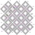
可选的,如图5a和图5b、图6a和图6b以及图10a所示,第一触控子电极1011和第二触控子电极1021均包括至少一个第一镂空区105。Optionally, as shown in FIG. 5 a and FIG. 5 b , FIG. 6 a and FIG. 6 b , and FIG. 10 a , each of the
虚拟电极104包括多个虚拟子电极1042,虚拟子电极1042与第一镂空区105一一对应;沿绝缘层103的厚度方向,一一对应的第一镂空区105的正投影覆盖虚拟子电极1042的正投影。The
当该触控结构10应用于触控显示装置时,第一镂空区105露出显示面板中亚像素的发光区。可以理解的是,该显示面板可以是上述的液晶显示面板1,也可以是电致发光显示面板3或者光致发光显示面板。When the
可选的,第一镂空区105的形状为任意规则图形,例如圆形、椭圆、三角形、四边形等多边形,此外,也可以是多种规则图形的组合。Optionally, the shape of the first
需要说明的是,沿绝缘层103的厚度方向,一一对应的第一镂空区105的正投影覆盖虚拟子电极1042的正投影指的是,沿绝缘层103的厚度方向,虚拟子电极1042的投影位于其对应的第一镂空区域105的投影的范围内。It should be noted that along the thickness direction of the insulating
其中,沿绝缘层103的厚度方向,虚拟子电极1042外轮廓的投影可以与第一镂空区域105的外轮廓的投影完全重合。Wherein, along the thickness direction of the insulating
在此基础上,可选的,如图5a和图5b、图6a和图6b所示,虚拟子电极1042包括第二镂空区1042a,第二镂空区1042a位于虚拟子电极1042的中部。即,虚拟子电极1042呈环形。其中,第二镂空区1042a的形状可以为任意规则图形,例如圆形、椭圆、三角形、四边形等多边形,此外,也可以是多种规则图形的组合。On this basis, optionally, as shown in FIG. 5 a and FIG. 5 b , FIG. 6 a and FIG. 6 b , the
通过在第一触控子电极1011和第二触控子电极1021均设置至少一个第一镂空区105,并在虚拟子电极1042设置第二镂空区1042a,能够使触控结构10应用于触控显示装置时,提高触控显示装置的光透过率。By setting at least one first
需要说明的是,为了便于理解,图5a-图5b以及图6a-图6b均以在第一触控子电极1011和第二触控子电极1021仅包括一个第一镂空区105,且第一镂空区域105为四边形,第二镂空区1042a为四边形进行示意。但在实际应用中,不限定第一镂空区域105的数量,和第一镂空区域105、第二镂空区域1042a的形状。It should be noted that, in order to facilitate understanding, Fig. 5a-Fig. 5b and Fig. 6a-Fig. The
可选的,第一触控电极1011和第二触控子电极1021、搭桥1022、虚拟电极104的材料均选自透明金属氧化物、金属、导电无机物或者导电有机物中的一种。Optionally, the materials of the
其中,金属可以包括金属单质、金属合金、金属纳米线等金属材料。Wherein, the metal may include metal materials such as simple metal, metal alloy, and metal nanowire.
示例的,金属材料可以为银(Ag)、铜(Cu)、铝(Al)、或铝铌合金(AlNb)合金等。Exemplarily, the metal material may be silver (Ag), copper (Cu), aluminum (Al), or aluminum-niobium alloy (AlNb) alloy, etc. FIG.
可选的,第一触控子电极1011和第二触控子电极1021均呈网格结构,且第一触控电极1011和第二触控电极1021的材料为金属单质或合金。Optionally, both the
网格结构中网格的形状为规则多边形或无规则多边形。如图7所示,以一个第一子触控电极1011为例,多根金属线交叉形成多个网格,对于任一个网格,其形状可以为规则多边形或无规则多边形。其中,网格的形状可以为如图7所示的菱形。当然也可以为矩形等其他形状。The shape of the grid in the grid structure is a regular polygon or an irregular polygon. As shown in FIG. 7 , taking a first
与透明金属氧化物、导电无机物和导电有机物相比,金属单质或合金的耐弯折性能更好,因而将触控结构10应用于柔性触控显示装置时,能够提高触控结构10的耐弯折性和可靠性。Compared with transparent metal oxides, conductive inorganic substances and conductive organic substances, the bending resistance of metal single substance or alloy is better, so when the
由于金属网格结构可透光,且金属材料的方阻较低可降低RC延迟,因而将触控结构10应用在大尺寸触控显示装置上,也能被IC(Integrated Circuit,集成电路)驱动,而且可达到较好的触控效果,支持多点触控。此外,金属材料的第一触控电极101和第二触控电极102,可防止ESD(Electrostatic Discharge,静电放电)。示例性的,金属材料的方阻小于等于0.3Ω/cm2。Since the metal grid structure can transmit light, and the low square resistance of the metal material can reduce the RC delay, the
对于应用到任一种尺寸的触控显示装置的触控结构10,在制作形成网格结构的第一触控电极101和第二触控电极102之前,首先需使用相关软件进行光学模拟,以使第一触控子电极1011和第二触控子电极1021的网格的参数与显示面板相匹配。例如对于菱形网格,要模拟出合适的菱形边长及菱形夹角,从而避免不匹配时,触控结构10应用于触控显示装置后,易出现干涉条纹的问题。For the
本发明实施例还提供一种触控基板,如图8所示,包括衬底8、设置于衬底6上的触控结构10,关于触控结构10与可参考上述的描述,在此不再赘述。The embodiment of the present invention also provides a touch control substrate, as shown in FIG. 8 , including a
该触控基板具有与上述触控结构10相同的有益效果。The touch control substrate has the same beneficial effects as the above
可选的,如图8所示,触控基板还包括设置于触控结构10远离衬底一侧的保护层7。Optionally, as shown in FIG. 8 , the touch substrate further includes a
其中,保护层7的材料例如可以为氧化硅、氮化硅、氮氧化硅中的一种或多种,可以用于保护触控结构10,以及可以使触控结构10的上表面平坦,方便后续在触控基板上制作其他膜层。Wherein, the material of the
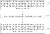
如图9所示,本发明实施例提供一种触控结构10的制备方法,包括:As shown in FIG. 9 , an embodiment of the present invention provides a method for manufacturing a
S10、如图10a所示,通过一次构图工艺形成多个间隔的第一触控电极101,第一触控电极101包括沿第一方向排布且直接连接的多个第一触控子电极1011;并形成多排第二触控子电极1021,每排中的第二触控子电极1021沿第二方向排布,第二触控子电极1021与第一触控电极101绝缘;第一方向和第二方向交叉。S10. As shown in FIG. 10a, a plurality of spaced
S11、如图10b所示,通过一次构图工艺形成绝缘层103,绝缘层103包括多个过孔。S11 , as shown in FIG. 10 b , an insulating
S12、如图10c所示,通过一次构图工艺形成多个间隔的搭桥1022和虚拟电极104,虚拟电极104与搭桥1022绝缘;沿第二方向,任意相邻第二触控子电极1021分别通过一个过孔与同一搭桥1022电连接,其中,每排中多个第二触控子电极1021以及电连接的多个搭桥1022构成一个第二触控电极102;虚拟电极104用于消影。S12. As shown in FIG. 10c, a plurality of spaced
如图11所示,本发明实施例还提供一种触控结构10的制备方法,包括:As shown in FIG. 11 , the embodiment of the present invention also provides a method for preparing a
S20、如图12a所示,通过一次构图工艺形成多个间隔的搭桥1022和虚拟电极104,虚拟电极104与搭桥104绝缘;虚拟电极104用于消影。S20 , as shown in FIG. 12 a , a plurality of spaced
S21、如图12b所示,通过一次构图工艺形成绝缘层103,绝缘层103包括多个过孔。S21 , as shown in FIG. 12 b , an insulating
S22、如图12c所示,通过一次构图工艺形成多个间隔的第一触控电极101,第一触控电极101包括沿第一方向排布且直接连接的多个第一触控子电极1011;并形成多排第二触控子电极1021,第二触控子电极1021与第一触控电极101绝缘;每排中的第二触控子电极1021沿第二方向排布,且每排中任意相邻第二触控子电极1021分别通过一个过孔与同一搭桥1022电连接;其中,每排中多个第二触控子电极1021以及电连接的多个搭桥1022构成一个第二触控电极102;第一方向和第二方向交叉。S22. As shown in FIG. 12c, a plurality of spaced
其中,构图工艺包括涂覆光刻胶、掩膜曝光、显影以及刻蚀工艺。Wherein, the patterning process includes coating photoresist, mask exposure, developing and etching processes.
可选的,第一方向和第二方向可以相互垂直。Optionally, the first direction and the second direction may be perpendicular to each other.
以上所述,仅为本发明的具体实施方式,但本发明的保护范围并不局限于此,任何熟悉本技术领域的技术人员在本发明揭露的技术范围内,可轻易想到变化或替换,都应涵盖在本发明的保护范围之内。因此,本发明的保护范围应以所述权利要求的保护范围为准。The above is only a specific embodiment of the present invention, but the scope of protection of the present invention is not limited thereto. Anyone skilled in the art can easily think of changes or substitutions within the technical scope disclosed in the present invention. Should be covered within the protection scope of the present invention. Therefore, the protection scope of the present invention should be determined by the protection scope of the claims.
Claims (12)
Translated fromChinesePriority Applications (2)
| Application Number | Priority Date | Filing Date | Title |
|---|---|---|---|
| CN201910755780.3ACN110471568B (en) | 2019-08-15 | 2019-08-15 | Touch structure, touch display device and preparation method of touch display device |
| US16/993,384US11340745B2 (en) | 2019-08-15 | 2020-08-14 | Touch structure and method for manufacturing the same, touch substrate and touch display device |
Applications Claiming Priority (1)
| Application Number | Priority Date | Filing Date | Title |
|---|---|---|---|
| CN201910755780.3ACN110471568B (en) | 2019-08-15 | 2019-08-15 | Touch structure, touch display device and preparation method of touch display device |
Publications (2)
| Publication Number | Publication Date |
|---|---|
| CN110471568A CN110471568A (en) | 2019-11-19 |
| CN110471568Btrue CN110471568B (en) | 2023-06-02 |
Family
ID=68510272
Family Applications (1)
| Application Number | Title | Priority Date | Filing Date |
|---|---|---|---|
| CN201910755780.3AActiveCN110471568B (en) | 2019-08-15 | 2019-08-15 | Touch structure, touch display device and preparation method of touch display device |
Country Status (2)
| Country | Link |
|---|---|
| US (1) | US11340745B2 (en) |
| CN (1) | CN110471568B (en) |
Families Citing this family (10)
| Publication number | Priority date | Publication date | Assignee | Title |
|---|---|---|---|---|
| WO2021102798A1 (en)* | 2019-11-28 | 2021-06-03 | 京东方科技集团股份有限公司 | Touch electrode structure, fabrication method therefor, touch panel, and electronic device |
| CN114253427B (en) | 2020-09-21 | 2023-12-08 | 京东方科技集团股份有限公司 | Touch structure, touch display panel and electronic device |
| CN114967957A (en)* | 2021-02-24 | 2022-08-30 | 京东方科技集团股份有限公司 | Display panel, touch display panel and display device |
| CN113220173B (en)* | 2021-05-28 | 2024-01-05 | 武汉天马微电子有限公司 | Display panel and display device |
| CN113741731B (en) | 2021-08-30 | 2023-09-05 | 武汉华星光电半导体显示技术有限公司 | display panel |
| CN115148930A (en)* | 2022-06-28 | 2022-10-04 | 武汉华星光电半导体显示技术有限公司 | Display panel |
| CN115268698A (en)* | 2022-08-10 | 2022-11-01 | 京东方科技集团股份有限公司 | Display device and touch structure |
| WO2024092405A1 (en)* | 2022-10-31 | 2024-05-10 | 京东方科技集团股份有限公司 | Touch structure, touch display panel and electronic device |
| CN116301435A (en)* | 2023-03-24 | 2023-06-23 | 昆山国显光电有限公司 | Display panel and display device |
| CN116560124A (en) | 2023-04-19 | 2023-08-08 | 天马微电子股份有限公司 | Display panel, driving method thereof and display device |
Citations (3)
| Publication number | Priority date | Publication date | Assignee | Title |
|---|---|---|---|---|
| WO2017045339A1 (en)* | 2015-09-15 | 2017-03-23 | 京东方科技集团股份有限公司 | Array substrate, display panel and display device |
| CN106886094A (en)* | 2015-12-15 | 2017-06-23 | 深圳超多维光电子有限公司 | Touch liquid crystal lens and its method of work, 3 d display device |
| CN108681414A (en)* | 2018-04-28 | 2018-10-19 | 京东方科技集团股份有限公司 | Touch base plate and preparation method thereof, touch control display apparatus |
Family Cites Families (25)
| Publication number | Priority date | Publication date | Assignee | Title |
|---|---|---|---|---|
| WO2013145958A1 (en)* | 2012-03-26 | 2013-10-03 | シャープ株式会社 | Touch panel substrate, display panel, and display apparatus |
| JP5270030B1 (en)* | 2012-09-24 | 2013-08-21 | 日本写真印刷株式会社 | Touch panel and method for manufacturing touch panel |
| TW201445379A (en)* | 2013-05-21 | 2014-12-01 | Wintek Corp | Touch panel |
| TW201512917A (en)* | 2013-09-23 | 2015-04-01 | Wintek Corp | Touch panel |
| JP5813831B1 (en)* | 2014-07-02 | 2015-11-17 | 日本航空電子工業株式会社 | Touch panel |
| TWI564761B (en)* | 2015-01-16 | 2017-01-01 | 友達光電股份有限公司 | Touch electrode layer |
| KR102325190B1 (en)* | 2015-04-13 | 2021-11-10 | 삼성디스플레이 주식회사 | Touch panel |
| CN104866142A (en)* | 2015-06-15 | 2015-08-26 | 合肥鑫晟光电科技有限公司 | Touch control base plate, preparing method of touch control base plate and display device |
| US10168844B2 (en)* | 2015-06-26 | 2019-01-01 | Samsung Display Co., Ltd. | Flexible display device |
| US10534481B2 (en)* | 2015-09-30 | 2020-01-14 | Apple Inc. | High aspect ratio capacitive sensor panel |
| CN205068345U (en)* | 2015-10-29 | 2016-03-02 | 合肥鑫晟光电科技有限公司 | Touch -control structure, touch screen and display device |
| CN105742330A (en)* | 2016-03-16 | 2016-07-06 | 京东方科技集团股份有限公司 | Organic light emitting display panel, fabrication method thereof and display device |
| CN106354299B (en)* | 2016-08-17 | 2019-04-26 | 京东方科技集团股份有限公司 | A touch substrate, a preparation method thereof, and a touch display device |
| CN106125993B (en)* | 2016-08-25 | 2019-05-10 | 京东方科技集团股份有限公司 | Manufacturing method of touch screen and conductive peelable adhesive |
| CN206193735U (en)* | 2016-11-22 | 2017-05-24 | 合肥鑫晟光电科技有限公司 | Touch substrate and display device |
| US10073294B1 (en)* | 2017-03-31 | 2018-09-11 | Innolux Corporation | Display device |
| CN107066160A (en)* | 2017-05-16 | 2017-08-18 | 京东方科技集团股份有限公司 | Touch base plate and preparation method thereof, display device |
| CN109407869B (en)* | 2017-08-15 | 2021-11-09 | 京东方科技集团股份有限公司 | Touch structure, preparation method thereof and display device |
| CN107479754B (en)* | 2017-08-22 | 2020-07-28 | 武汉天马微电子有限公司 | Flexible touch sensor and flexible touch display panel |
| CN108089768A (en)* | 2018-01-25 | 2018-05-29 | 武汉华星光电半导体显示技术有限公司 | Touch panel structure provided and flexible touch display device |
| KR101952769B1 (en)* | 2018-02-28 | 2019-02-27 | 동우 화인켐 주식회사 | Touch sensor |
| CN108646952B (en)* | 2018-03-29 | 2021-07-30 | 上海天马微电子有限公司 | Touch display panel and touch display device |
| CN108710447A (en)* | 2018-05-14 | 2018-10-26 | 京东方科技集团股份有限公司 | A kind of touch-control structure and display screen |
| KR102632590B1 (en)* | 2018-10-16 | 2024-02-05 | 삼성디스플레이 주식회사 | Touch sensor and display device comprising the touch sensor |
| CN109901747B (en)* | 2019-02-26 | 2022-03-11 | 上海天马微电子有限公司 | Display panel and display device |
- 2019
- 2019-08-15CNCN201910755780.3Apatent/CN110471568B/enactiveActive
- 2020
- 2020-08-14USUS16/993,384patent/US11340745B2/enactiveActive
Patent Citations (3)
| Publication number | Priority date | Publication date | Assignee | Title |
|---|---|---|---|---|
| WO2017045339A1 (en)* | 2015-09-15 | 2017-03-23 | 京东方科技集团股份有限公司 | Array substrate, display panel and display device |
| CN106886094A (en)* | 2015-12-15 | 2017-06-23 | 深圳超多维光电子有限公司 | Touch liquid crystal lens and its method of work, 3 d display device |
| CN108681414A (en)* | 2018-04-28 | 2018-10-19 | 京东方科技集团股份有限公司 | Touch base plate and preparation method thereof, touch control display apparatus |
Non-Patent Citations (5)
| Title |
|---|
| Munehiko Sato.Zensei: Embedded, Multi-electrode Bioimpedance Sensing for Implicit, Ubiquitous User Recognition.Environmental Sensing.2017,全文.* |
| Shuo Gao.A Multi-functional Touch Panel for Multi-Dimensional Sensing in Interactive Displays.《A thesis presented for the degree of Doctor of Philosophy》.2017,全文.* |
| 蒋晶晶;丁辛.电容式柔性触控装置的研制.纺织学报.2013,(09),全文.* |
| 谢江容;潘风明;吴政南;谢杰;潘兴修.投射式电容触摸屏的电极设计分析.光电子技术.2016,(03),全文.* |
| 赵重阳;苏秋杰;缪应蒙;高玉杰;王永垚;朱宁;廖燕平;邵喜斌.TFT-LCD中像素电极耦合电容对显示画质的影响.液晶与显示.2019,(05),全文.* |
Also Published As
| Publication number | Publication date |
|---|---|
| CN110471568A (en) | 2019-11-19 |
| US11340745B2 (en) | 2022-05-24 |
| US20210048925A1 (en) | 2021-02-18 |
Similar Documents
| Publication | Publication Date | Title |
|---|---|---|
| CN110471568B (en) | Touch structure, touch display device and preparation method of touch display device | |
| CN113424325B (en) | Touch display panel and electronic device | |
| CN108054193B (en) | Flexible display panel and flexible display device | |
| US10852897B2 (en) | Touch panel and touch display device | |
| CN108258010B (en) | display device | |
| CN111261679B (en) | A touch panel, a preparation method thereof, and a touch display device | |
| CN104238815A (en) | Display panel, driving method for same and display device | |
| CN110703941B (en) | Touch structure, preparation method thereof, touch substrate and touch display device | |
| CN112711354B (en) | Touch panel, manufacturing method thereof, and display touch device | |
| CN215494957U (en) | Touch panel and display touch device | |
| US11782558B2 (en) | Touch structure, touch display panel and electronic device | |
| CN106293200A (en) | A kind of cover plate and preparation method thereof, display device | |
| CN117063144A (en) | Touch structure, touch display panel and display device | |
| CN118139481A (en) | Display panel and display terminal | |
| WO2022052777A1 (en) | Touch structure, display panel and electronic device | |
| CN114096939B (en) | Touch structure, touch display panel and electronic device | |
| WO2025180132A1 (en) | Touch display panel and display device | |
| WO2022179190A1 (en) | Touch-control panel and preparation method therefor, and display touch-control apparatus | |
| JP7645227B2 (en) | Touch structure, touch display panel and electronic device | |
| CN113728296B (en) | Touch substrate and touch display device | |
| CN209417707U (en) | A touch structure and a touch display device | |
| CN112328119A (en) | Touch structure and touch display panel | |
| KR20220075010A (en) | Display device | |
| CN219644497U (en) | Display panel and display device | |
| US20250138689A1 (en) | Touch layer group and touch display apparatus |
Legal Events
| Date | Code | Title | Description |
|---|---|---|---|
| PB01 | Publication | ||
| PB01 | Publication | ||
| SE01 | Entry into force of request for substantive examination | ||
| SE01 | Entry into force of request for substantive examination | ||
| GR01 | Patent grant | ||
| GR01 | Patent grant |