CN110379761B - Micro-LED transfer substrate and device - Google Patents
Micro-LED transfer substrate and deviceDownload PDFInfo
- Publication number
- CN110379761B CN110379761BCN201910651165.8ACN201910651165ACN110379761BCN 110379761 BCN110379761 BCN 110379761BCN 201910651165 ACN201910651165 ACN 201910651165ACN 110379761 BCN110379761 BCN 110379761B
- Authority
- CN
- China
- Prior art keywords
- electrode
- micro
- transfer
- film layer
- thin film
- Prior art date
- Legal status (The legal status is an assumption and is not a legal conclusion. Google has not performed a legal analysis and makes no representation as to the accuracy of the status listed.)
- Active
Links
Images


Classifications
- H—ELECTRICITY
- H01—ELECTRIC ELEMENTS
- H01L—SEMICONDUCTOR DEVICES NOT COVERED BY CLASS H10
- H01L21/00—Processes or apparatus adapted for the manufacture or treatment of semiconductor or solid state devices or of parts thereof
- H01L21/67—Apparatus specially adapted for handling semiconductor or electric solid state devices during manufacture or treatment thereof; Apparatus specially adapted for handling wafers during manufacture or treatment of semiconductor or electric solid state devices or components ; Apparatus not specifically provided for elsewhere
- H01L21/683—Apparatus specially adapted for handling semiconductor or electric solid state devices during manufacture or treatment thereof; Apparatus specially adapted for handling wafers during manufacture or treatment of semiconductor or electric solid state devices or components ; Apparatus not specifically provided for elsewhere for supporting or gripping
- H01L21/6835—Apparatus specially adapted for handling semiconductor or electric solid state devices during manufacture or treatment thereof; Apparatus specially adapted for handling wafers during manufacture or treatment of semiconductor or electric solid state devices or components ; Apparatus not specifically provided for elsewhere for supporting or gripping using temporarily an auxiliary support
- H—ELECTRICITY
- H01—ELECTRIC ELEMENTS
- H01L—SEMICONDUCTOR DEVICES NOT COVERED BY CLASS H10
- H01L25/00—Assemblies consisting of a plurality of semiconductor or other solid state devices
- H01L25/03—Assemblies consisting of a plurality of semiconductor or other solid state devices all the devices being of a type provided for in a single subclass of subclasses H10B, H10D, H10F, H10H, H10K or H10N, e.g. assemblies of rectifier diodes
- H01L25/04—Assemblies consisting of a plurality of semiconductor or other solid state devices all the devices being of a type provided for in a single subclass of subclasses H10B, H10D, H10F, H10H, H10K or H10N, e.g. assemblies of rectifier diodes the devices not having separate containers
- H01L25/075—Assemblies consisting of a plurality of semiconductor or other solid state devices all the devices being of a type provided for in a single subclass of subclasses H10B, H10D, H10F, H10H, H10K or H10N, e.g. assemblies of rectifier diodes the devices not having separate containers the devices being of a type provided for in group H10H20/00
- H01L25/0753—Assemblies consisting of a plurality of semiconductor or other solid state devices all the devices being of a type provided for in a single subclass of subclasses H10B, H10D, H10F, H10H, H10K or H10N, e.g. assemblies of rectifier diodes the devices not having separate containers the devices being of a type provided for in group H10H20/00 the devices being arranged next to each other
- H—ELECTRICITY
- H01—ELECTRIC ELEMENTS
- H01L—SEMICONDUCTOR DEVICES NOT COVERED BY CLASS H10
- H01L21/00—Processes or apparatus adapted for the manufacture or treatment of semiconductor or solid state devices or of parts thereof
- H01L21/67—Apparatus specially adapted for handling semiconductor or electric solid state devices during manufacture or treatment thereof; Apparatus specially adapted for handling wafers during manufacture or treatment of semiconductor or electric solid state devices or components ; Apparatus not specifically provided for elsewhere
- H01L21/67005—Apparatus not specifically provided for elsewhere
- H01L21/67011—Apparatus for manufacture or treatment
- H01L21/67138—Apparatus for wiring semiconductor or solid state device
- H—ELECTRICITY
- H01—ELECTRIC ELEMENTS
- H01L—SEMICONDUCTOR DEVICES NOT COVERED BY CLASS H10
- H01L21/00—Processes or apparatus adapted for the manufacture or treatment of semiconductor or solid state devices or of parts thereof
- H01L21/67—Apparatus specially adapted for handling semiconductor or electric solid state devices during manufacture or treatment thereof; Apparatus specially adapted for handling wafers during manufacture or treatment of semiconductor or electric solid state devices or components ; Apparatus not specifically provided for elsewhere
- H01L21/683—Apparatus specially adapted for handling semiconductor or electric solid state devices during manufacture or treatment thereof; Apparatus specially adapted for handling wafers during manufacture or treatment of semiconductor or electric solid state devices or components ; Apparatus not specifically provided for elsewhere for supporting or gripping
- H01L21/6831—Apparatus specially adapted for handling semiconductor or electric solid state devices during manufacture or treatment thereof; Apparatus specially adapted for handling wafers during manufacture or treatment of semiconductor or electric solid state devices or components ; Apparatus not specifically provided for elsewhere for supporting or gripping using electrostatic chucks
- H01L21/6833—Details of electrostatic chucks
- H—ELECTRICITY
- H01—ELECTRIC ELEMENTS
- H01L—SEMICONDUCTOR DEVICES NOT COVERED BY CLASS H10
- H01L24/00—Arrangements for connecting or disconnecting semiconductor or solid-state bodies; Methods or apparatus related thereto
- H01L24/74—Apparatus for manufacturing arrangements for connecting or disconnecting semiconductor or solid-state bodies
- H01L24/75—Apparatus for connecting with bump connectors or layer connectors
- H—ELECTRICITY
- H01—ELECTRIC ELEMENTS
- H01L—SEMICONDUCTOR DEVICES NOT COVERED BY CLASS H10
- H01L24/00—Arrangements for connecting or disconnecting semiconductor or solid-state bodies; Methods or apparatus related thereto
- H01L24/93—Batch processes
- H01L24/95—Batch processes at chip-level, i.e. with connecting carried out on a plurality of singulated devices, i.e. on diced chips
- H—ELECTRICITY
- H10—SEMICONDUCTOR DEVICES; ELECTRIC SOLID-STATE DEVICES NOT OTHERWISE PROVIDED FOR
- H10H—INORGANIC LIGHT-EMITTING SEMICONDUCTOR DEVICES HAVING POTENTIAL BARRIERS
- H10H29/00—Integrated devices, or assemblies of multiple devices, comprising at least one light-emitting semiconductor element covered by group H10H20/00
- H10H29/10—Integrated devices comprising at least one light-emitting semiconductor component covered by group H10H20/00
- H10H29/14—Integrated devices comprising at least one light-emitting semiconductor component covered by group H10H20/00 comprising multiple light-emitting semiconductor components
- H10H29/142—Two-dimensional arrangements, e.g. asymmetric LED layout
- H—ELECTRICITY
- H01—ELECTRIC ELEMENTS
- H01L—SEMICONDUCTOR DEVICES NOT COVERED BY CLASS H10
- H01L2221/00—Processes or apparatus adapted for the manufacture or treatment of semiconductor or solid state devices or of parts thereof covered by H01L21/00
- H01L2221/67—Apparatus for handling semiconductor or electric solid state devices during manufacture or treatment thereof; Apparatus for handling wafers during manufacture or treatment of semiconductor or electric solid state devices or components; Apparatus not specifically provided for elsewhere
- H01L2221/683—Apparatus for handling semiconductor or electric solid state devices during manufacture or treatment thereof; Apparatus for handling wafers during manufacture or treatment of semiconductor or electric solid state devices or components; Apparatus not specifically provided for elsewhere for supporting or gripping
- H01L2221/68304—Apparatus for handling semiconductor or electric solid state devices during manufacture or treatment thereof; Apparatus for handling wafers during manufacture or treatment of semiconductor or electric solid state devices or components; Apparatus not specifically provided for elsewhere for supporting or gripping using temporarily an auxiliary support
- H01L2221/68318—Auxiliary support including means facilitating the separation of a device or wafer from the auxiliary support
- H01L2221/68322—Auxiliary support including means facilitating the selective separation of some of a plurality of devices from the auxiliary support
- H—ELECTRICITY
- H01—ELECTRIC ELEMENTS
- H01L—SEMICONDUCTOR DEVICES NOT COVERED BY CLASS H10
- H01L2221/00—Processes or apparatus adapted for the manufacture or treatment of semiconductor or solid state devices or of parts thereof covered by H01L21/00
- H01L2221/67—Apparatus for handling semiconductor or electric solid state devices during manufacture or treatment thereof; Apparatus for handling wafers during manufacture or treatment of semiconductor or electric solid state devices or components; Apparatus not specifically provided for elsewhere
- H01L2221/683—Apparatus for handling semiconductor or electric solid state devices during manufacture or treatment thereof; Apparatus for handling wafers during manufacture or treatment of semiconductor or electric solid state devices or components; Apparatus not specifically provided for elsewhere for supporting or gripping
- H01L2221/68304—Apparatus for handling semiconductor or electric solid state devices during manufacture or treatment thereof; Apparatus for handling wafers during manufacture or treatment of semiconductor or electric solid state devices or components; Apparatus not specifically provided for elsewhere for supporting or gripping using temporarily an auxiliary support
- H01L2221/68354—Apparatus for handling semiconductor or electric solid state devices during manufacture or treatment thereof; Apparatus for handling wafers during manufacture or treatment of semiconductor or electric solid state devices or components; Apparatus not specifically provided for elsewhere for supporting or gripping using temporarily an auxiliary support used to support diced chips prior to mounting
- H—ELECTRICITY
- H01—ELECTRIC ELEMENTS
- H01L—SEMICONDUCTOR DEVICES NOT COVERED BY CLASS H10
- H01L2221/00—Processes or apparatus adapted for the manufacture or treatment of semiconductor or solid state devices or of parts thereof covered by H01L21/00
- H01L2221/67—Apparatus for handling semiconductor or electric solid state devices during manufacture or treatment thereof; Apparatus for handling wafers during manufacture or treatment of semiconductor or electric solid state devices or components; Apparatus not specifically provided for elsewhere
- H01L2221/683—Apparatus for handling semiconductor or electric solid state devices during manufacture or treatment thereof; Apparatus for handling wafers during manufacture or treatment of semiconductor or electric solid state devices or components; Apparatus not specifically provided for elsewhere for supporting or gripping
- H01L2221/68304—Apparatus for handling semiconductor or electric solid state devices during manufacture or treatment thereof; Apparatus for handling wafers during manufacture or treatment of semiconductor or electric solid state devices or components; Apparatus not specifically provided for elsewhere for supporting or gripping using temporarily an auxiliary support
- H01L2221/68363—Apparatus for handling semiconductor or electric solid state devices during manufacture or treatment thereof; Apparatus for handling wafers during manufacture or treatment of semiconductor or electric solid state devices or components; Apparatus not specifically provided for elsewhere for supporting or gripping using temporarily an auxiliary support used in a transfer process involving transfer directly from an origin substrate to a target substrate without use of an intermediate handle substrate
- H—ELECTRICITY
- H01—ELECTRIC ELEMENTS
- H01L—SEMICONDUCTOR DEVICES NOT COVERED BY CLASS H10
- H01L2221/00—Processes or apparatus adapted for the manufacture or treatment of semiconductor or solid state devices or of parts thereof covered by H01L21/00
- H01L2221/67—Apparatus for handling semiconductor or electric solid state devices during manufacture or treatment thereof; Apparatus for handling wafers during manufacture or treatment of semiconductor or electric solid state devices or components; Apparatus not specifically provided for elsewhere
- H01L2221/683—Apparatus for handling semiconductor or electric solid state devices during manufacture or treatment thereof; Apparatus for handling wafers during manufacture or treatment of semiconductor or electric solid state devices or components; Apparatus not specifically provided for elsewhere for supporting or gripping
- H01L2221/68304—Apparatus for handling semiconductor or electric solid state devices during manufacture or treatment thereof; Apparatus for handling wafers during manufacture or treatment of semiconductor or electric solid state devices or components; Apparatus not specifically provided for elsewhere for supporting or gripping using temporarily an auxiliary support
- H01L2221/68368—Apparatus for handling semiconductor or electric solid state devices during manufacture or treatment thereof; Apparatus for handling wafers during manufacture or treatment of semiconductor or electric solid state devices or components; Apparatus not specifically provided for elsewhere for supporting or gripping using temporarily an auxiliary support used in a transfer process involving at least two transfer steps, i.e. including an intermediate handle substrate
- H—ELECTRICITY
- H01—ELECTRIC ELEMENTS
- H01L—SEMICONDUCTOR DEVICES NOT COVERED BY CLASS H10
- H01L2221/00—Processes or apparatus adapted for the manufacture or treatment of semiconductor or solid state devices or of parts thereof covered by H01L21/00
- H01L2221/67—Apparatus for handling semiconductor or electric solid state devices during manufacture or treatment thereof; Apparatus for handling wafers during manufacture or treatment of semiconductor or electric solid state devices or components; Apparatus not specifically provided for elsewhere
- H01L2221/683—Apparatus for handling semiconductor or electric solid state devices during manufacture or treatment thereof; Apparatus for handling wafers during manufacture or treatment of semiconductor or electric solid state devices or components; Apparatus not specifically provided for elsewhere for supporting or gripping
- H01L2221/68304—Apparatus for handling semiconductor or electric solid state devices during manufacture or treatment thereof; Apparatus for handling wafers during manufacture or treatment of semiconductor or electric solid state devices or components; Apparatus not specifically provided for elsewhere for supporting or gripping using temporarily an auxiliary support
- H01L2221/68381—Details of chemical or physical process used for separating the auxiliary support from a device or wafer
- H—ELECTRICITY
- H01—ELECTRIC ELEMENTS
- H01L—SEMICONDUCTOR DEVICES NOT COVERED BY CLASS H10
- H01L2224/00—Indexing scheme for arrangements for connecting or disconnecting semiconductor or solid-state bodies and methods related thereto as covered by H01L24/00
- H01L2224/74—Apparatus for manufacturing arrangements for connecting or disconnecting semiconductor or solid-state bodies and for methods related thereto
- H01L2224/75—Apparatus for connecting with bump connectors or layer connectors
- H01L2224/757—Means for aligning
- H01L2224/75723—Electrostatic holding means
- H01L2224/75724—Electrostatic holding means in the lower part of the bonding apparatus, e.g. in the apparatus chuck
- H—ELECTRICITY
- H01—ELECTRIC ELEMENTS
- H01L—SEMICONDUCTOR DEVICES NOT COVERED BY CLASS H10
- H01L2224/00—Indexing scheme for arrangements for connecting or disconnecting semiconductor or solid-state bodies and methods related thereto as covered by H01L24/00
- H01L2224/74—Apparatus for manufacturing arrangements for connecting or disconnecting semiconductor or solid-state bodies and for methods related thereto
- H01L2224/75—Apparatus for connecting with bump connectors or layer connectors
- H01L2224/757—Means for aligning
- H01L2224/75754—Guiding structures
- H01L2224/75755—Guiding structures in the lower part of the bonding apparatus, e.g. in the apparatus chuck
- H—ELECTRICITY
- H01—ELECTRIC ELEMENTS
- H01L—SEMICONDUCTOR DEVICES NOT COVERED BY CLASS H10
- H01L2224/00—Indexing scheme for arrangements for connecting or disconnecting semiconductor or solid-state bodies and methods related thereto as covered by H01L24/00
- H01L2224/74—Apparatus for manufacturing arrangements for connecting or disconnecting semiconductor or solid-state bodies and for methods related thereto
- H01L2224/75—Apparatus for connecting with bump connectors or layer connectors
- H01L2224/7598—Apparatus for connecting with bump connectors or layer connectors specially adapted for batch processes
- H—ELECTRICITY
- H01—ELECTRIC ELEMENTS
- H01L—SEMICONDUCTOR DEVICES NOT COVERED BY CLASS H10
- H01L2224/00—Indexing scheme for arrangements for connecting or disconnecting semiconductor or solid-state bodies and methods related thereto as covered by H01L24/00
- H01L2224/93—Batch processes
- H01L2224/95—Batch processes at chip-level, i.e. with connecting carried out on a plurality of singulated devices, i.e. on diced chips
- H01L2224/95001—Batch processes at chip-level, i.e. with connecting carried out on a plurality of singulated devices, i.e. on diced chips involving a temporary auxiliary member not forming part of the bonding apparatus, e.g. removable or sacrificial coating, film or substrate
- H—ELECTRICITY
- H01—ELECTRIC ELEMENTS
- H01L—SEMICONDUCTOR DEVICES NOT COVERED BY CLASS H10
- H01L2924/00—Indexing scheme for arrangements or methods for connecting or disconnecting semiconductor or solid-state bodies as covered by H01L24/00
- H01L2924/10—Details of semiconductor or other solid state devices to be connected
- H01L2924/11—Device type
- H01L2924/12—Passive devices, e.g. 2 terminal devices
- H01L2924/1204—Optical Diode
- H01L2924/12041—LED
Landscapes
- Engineering & Computer Science (AREA)
- Microelectronics & Electronic Packaging (AREA)
- Power Engineering (AREA)
- Computer Hardware Design (AREA)
- Physics & Mathematics (AREA)
- Condensed Matter Physics & Semiconductors (AREA)
- General Physics & Mathematics (AREA)
- Manufacturing & Machinery (AREA)
- Led Device Packages (AREA)
Abstract
Translated fromChinese
Description
Translated fromChinese技术领域technical field
本发明属于显示技术领域,具体涉及一种微发光二极管转移基板及装置。The invention belongs to the field of display technology, and in particular relates to a micro-light emitting diode transfer substrate and a device.
背景技术Background technique
微发光二极管(micro light emitting diode,Micro–LED)显示技术是将传统的显示器件进行微小化和矩阵化,并采用集成电路工艺制成驱动电路,以实现每一个像素点定址控制和单独驱动的显示技术。由于其亮度、寿命、对比度、反应时间、能耗、可视角度和分辨率等各种指标均由于传统的显示技术。并且其属于自发光、结构简单、体积小以及节能的优点,被视为下一代显示技术。Micro light emitting diode (Micro-LED) display technology is to miniaturize and matrix traditional display devices, and use integrated circuit technology to make driving circuits to achieve address control and individual driving of each pixel. display technology. Due to its various indicators such as brightness, life, contrast, response time, energy consumption, viewing angle and resolution are due to traditional display technology. And it belongs to the advantages of self-luminescence, simple structure, small size and energy saving, and is regarded as the next generation display technology.
目前制作Micro-LED显示面板的过程中,首先在转移基板上形成微发光二极管,再将巨量的微发光二极管转移至接收基板,实现微发光二极管的巨量转移。In the current process of manufacturing Micro-LED display panels, micro-LEDs are first formed on a transfer substrate, and then a huge amount of micro-LEDs is transferred to a receiving substrate to realize the massive transfer of micro-LEDs.
发明人发现现有技术中至少存在如下问题:现有的微发光二极管元件巨量转移普遍精确度不高,微发光二极管元件之间的间距较大,不能满足巨量转移对高精确度的要求。The inventors found that there are at least the following problems in the prior art: the mass transfer of the existing micro-LED elements is generally not high in accuracy, and the distance between the micro-LED elements is relatively large, which cannot meet the high-accuracy requirements for mass transfer. .
发明内容SUMMARY OF THE INVENTION
本发明旨在至少解决现有技术中存在的技术问题之一,提供一种微发光二极管转移基板及装置。The present invention aims to solve at least one of the technical problems existing in the prior art, and provides a micro-LED transfer substrate and a device.
解决本发明技术问题所采用的技术方案是一种微发光二极管转移基板,该微发光二极管转移基板包括:The technical solution adopted to solve the technical problem of the present invention is a micro-LED transfer substrate, the micro-LED transfer substrate includes:
基底,具有间隔设置多个基座;所述基座,用于承载待进行转移的微发光二极管;a base, with a plurality of bases arranged at intervals; the bases are used to carry the micro-light-emitting diodes to be transferred;
调距单元,设置在两相邻所述基座之间,用于调整所述基座之间的距离。The distance adjusting unit is arranged between two adjacent bases and is used to adjust the distance between the bases.
可选地,所述调距单元,包括:相对设置的第一起电结构和第二起电结构;其中,Optionally, the distance adjustment unit includes: a first electrification structure and a second electrification structure arranged oppositely; wherein,
所述第一起电结构和所述第二起电结构的两端分别连接两相邻的所述基座,且二者在外力的作用下发生形变,并能够在相互接触时产生不同极性的电荷。The two ends of the first electrification structure and the second electrification structure are respectively connected to the two adjacent bases, and the two are deformed under the action of external force, and can produce different polarities when they contact each other. charge.
可选地,所述第一起电结构包括:第一电极,设置在所述第一电极上的第一薄膜层;Optionally, the first electrification structure includes: a first electrode, and a first thin film layer disposed on the first electrode;
所述第二起电结构包括:与所述第一电极相对设置的第二电极,设置在所述第二电极靠近所述第一电极的侧面上的第二薄膜层;其中,The second electrification structure includes: a second electrode arranged opposite to the first electrode, and a second thin film layer arranged on the side of the second electrode close to the first electrode; wherein,
所述第一薄膜层和所述第二薄膜层的介电常数不同。The dielectric constants of the first thin film layer and the second thin film layer are different.
可选地,在所述基座上设置有转移电极;其中,Optionally, a transfer electrode is provided on the base; wherein,
所述转移电极与所述第一电极电连接。The transfer electrode is electrically connected to the first electrode.
可选地,所述转移电极与所述第一电极为一体式结构。Optionally, the transfer electrode and the first electrode are of an integral structure.
可选地,所述转移电极的材料包括:铜。Optionally, the material of the transfer electrode includes: copper.
可选地,所述第一薄膜层的材料包括聚酰亚胺;所述第二薄膜层的材料包括聚对苯二甲酸乙二醇酯。Optionally, the material of the first thin film layer includes polyimide; the material of the second thin film layer includes polyethylene terephthalate.
可选地,所述基座与待进行转移的所述微发光二极管一一对应。Optionally, the bases are in one-to-one correspondence with the micro-LEDs to be transferred.
解决本发明技术问题所采用的技术方案是一种微发光二极管转移装置,该微发光二极管转移装置上述提供的微发光二极管转移基板。The technical solution adopted to solve the technical problem of the present invention is a micro-LED transfer device, which is the micro-LED transfer substrate provided above.
可选地,该微光二极管转移装置还包括推动模块,与所述调距单元连接,用于为所述调距单元施加外力,以使所述调距单元对所述基座之间的距离进行调整。Optionally, the micro-light diode transfer device further includes a push module, which is connected to the distance adjustment unit and is used to apply an external force to the distance adjustment unit, so as to make the distance between the distance adjustment unit and the base. make adjustments.
附图说明Description of drawings
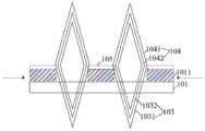
图1a、图1b、图3a和图3b为本发明实施例提供的一种微发光二极管转移基板的侧视结构示意图;1a, 1b, 3a and 3b are schematic side views of the structure of a micro-LED transfer substrate according to an embodiment of the present invention;
图2a和图2b为本发明实施例提供的一种微发光二极管转移基板的俯视结构示意图。2a and 2b are schematic top-view structural diagrams of a micro-LED transfer substrate according to an embodiment of the present invention.
其中附图标记为:101-基底、102-调距单元、103-第一起电结构、104-第二起电结构、105-转移电极、1011-基座、1031-第一电极、1032-第一薄膜层、1041-第二电极、及1042-第二薄膜层。The reference numerals are: 101-substrate, 102-pitch unit, 103-first electrification structure, 104-second electrification structure, 105-transfer electrode, 1011-base, 1031-first electrode, 1032-th A thin film layer, 1041 - the second electrode, and 1042 - the second thin film layer.
具体实施方式Detailed ways
为使本领域技术人员更好地理解本发明的技术方案,下面结合附图和具体实施方式对本发明作进一步详细描述。In order to make those skilled in the art better understand the technical solutions of the present invention, the present invention will be further described in detail below with reference to the accompanying drawings and specific embodiments.
实施例一Example 1
本发明实施例提供了一种微发光二极管转移基板,可以用于微发光二极管显示面板制作过程中的微发光二极管的巨量转移,图1a和图1b为本发明实施例提供的一种微发光二极管转移基板的侧视结构示意图,如图1a和图1b所示,本发明实施例提供的微发光二极管转移基板包括:基底101和调距单元102。基底101具有间隔设置多个基座1011;基座1011用于承载待进行转移的微发光二极管;调距单元102设置在两相邻基座1011之间,用于调整基座1011之间的距离。The embodiment of the present invention provides a micro-LED transfer substrate, which can be used for mass transfer of micro-LEDs in the process of manufacturing a micro-LED display panel. A schematic side view of the structure of the diode transfer substrate is shown in FIG. 1 a and FIG. 1 b . The
本发明实施例提供的微发光二极管转移基板,在初始状态时,通过施加外力使得设置在两个基座1011之间调距单元102处于伸展状态,从而使得相邻的两个基座1011之间的距离处于最大距离。在实际应用中,相邻的两个基座1011之间的最大距离可以为现有技术中相邻的两个待进行转移的微发光二极管之间可以达到的距离。然后,利用沉积方式,在基底101的基座1011位置上对应制作微发光二极管,形成巨量的呈矩阵式排列的微发光二极管。微发光二极管制作完成后,通过施加外力使得设置在两个基座1011之间的调距单元102收缩至一定程度,从而使得相邻的两个基座1011之间的距离缩短至最小,进而使得在基座1011上的微发光二极管之间的距离缩短。最后,将基座1011上的待进行转移的微发光二极管进行转移。图2a和图2b为本发明实施例提供的一种微发光二极管转移基板的俯视结构示意图,由图2a和图2b可以看出,本发明实施例提供的微发光二极管转移基板,通过调距单元102可以缩短相邻的基座1011之间的距离,从而缩短待进行转移的微发光二极管之间的距离,进而提高微发光二极管巨量转移的精确度,实现微发光二极管的高精确度的巨量转移。并且,在制作微发光二极管时,调距单元102处于伸展状态,因此微发光二极管之间的距离较大,对于加工精确度要求较低,从而可以降低微发光二极管的制作难度,节约制作成本。In the initial state of the micro-LED transfer substrate provided by the embodiment of the present invention, the distance-adjusting
在一个具体的例子中,如图3a和图3b所示,该调距单元102可以包括:相对设置的第一起电结构103和第二起电结构104;其中,第一起电结构103和第二起电结构104的两端分别连接两相邻的基座1011,且二者在外力的作用下发生形变,并能够在相互接触时产生不同极性的电荷。In a specific example, as shown in FIG. 3a and FIG. 3b, the
需要说明的是,在本发明实施例中,调距单元102由相对设置的第一起电结构103和第二起电结构104组成。在初始状态时,通过施加外力,可以使得第一起电结构103和第二起电结构104沿着平行于基底101所在平面方向上处于伸展状态,并相互接触,该外力的方向可以是垂直于基底101所在平面方向。可以将第一起电结构103和第二起电结构104反复的伸展与收缩,由于摩擦起电效应,在第一起电结构103和第二起电结构104接触的表面可以产生数量相等、极性相反的电荷。此时,由于第一起电结构103和第二起电结构104之间具有一定的间隙,该间隙较小,并小于预设的临界值,第一起电结构103和第二起电结构104处于一个平衡态,可以使得电荷被屏蔽在第一起电结构103和第二起电结构104之间,而且不向外传导,也不进行中和。可以通过施加外力,根据微发光二极管显示面板上的微发光二极管的精度,可以使得第一起电单元103和第二起电单元104收缩至一定程度,第一起电单元103和第二起电单元104的接触面分离,从而使得相邻的基座1011之间的距离缩短,进而使得相邻的待进行转移的微发光二极管之间的距离缩短。此时,第一起电结构103和第二起电结构104处于之间处于分离状态,第一起电结构103和第二起电结构104之间的间隙较大,并大于预设的临界值,第一起电结构103和第二起电结构104的平衡态被打破,其中的电荷不被屏蔽,相应的电荷可以进行转移至微发光二极管相应的位置,使得产生的电荷可以用于对微发光二极管进行吸附,起到固定的作用。It should be noted that, in the embodiment of the present invention, the
具体地,如图3a和图3b所示,第一起电结构103包括:第一电极1031,设置在第一电极1031上的第一薄膜层1032;第二起电结构104包括:与第一电极1031相对设置的第二电极1041,设置在第二电极1041靠近第一电极1031的侧面上的第二薄膜层1042;其中,第一薄膜层1032和第二薄膜层1042的介电常数不同。Specifically, as shown in FIG. 3a and FIG. 3b, the
需要说明的是,第一薄膜层1032和第二薄膜层1042为两种介电常数不同的绝缘材料。在初始状态时,可以将第一薄膜层1032和第二薄膜层1042可以进行反复的伸展与收缩,由于摩擦起电效应,在第一薄膜层1032和第二薄膜层1042的表面可以产生数量相等且极性相反的电荷,此时,第一薄膜层1032和第二薄膜层1042之间的间隙较小,并小于预设的临界值,在第一薄膜层1032和第二薄膜层1042的界面出形成一个偶极层。由于第一薄膜层1032和第二薄膜层1042自身绝缘,所有的极性相反的电荷在界面处互相屏蔽,产生的电荷不会被传导或者被中和,处于平衡态。然后,通过施加外力,使得第一薄膜层1032和第二薄膜层1042分离,由于第一薄膜层1032和第二薄膜层1042处于分离状态,第一薄膜层1032和第二薄膜层1042之间的间隙较大,并大于预设的临界值,两个薄膜层上的极性相反的电荷不能完全屏蔽,产生电势差,此时,第一电极1031被诱导出与第一薄膜层1032产生的电荷的极性相反的电荷,第二电极1041被诱导出与第二薄膜层1042产生的电荷的极性相反的电荷,从而,第一电极1031和第二电极1041上的电荷的极性也相反。由于第一电极1031为导体,可以将诱导产生的相应极性的进行传导至基座1011位置处,利用静电对于微发光二极管的吸附能力,可以将微发光二极管进行固定,进而进行巨量转移。可以理解的是,第一电极1031和第二电极1042的可以在外力作用下使得其上的薄膜层相互接触或相互分离,其结构可以设置为如图3a和图3b所示的弯折形结构,也可以设置成圆弧形结构,也可以为其他形状的结构,在此不再一一列举。It should be noted that the first
可选地,基座1011上设置有转移电极105;其中,转移电极105与第一电极1031电连接。Optionally, a
需要说明的是,转移电极105与第一电极1031电连接,可以将第一电极1031诱导出相应极性的电荷传导至基座1011上的转移电极,从而转移电极105上的电荷与第一电极1031上的电荷的极性相同。并且,转移电极105和第一电极1031一般为同材质的材料制成,同材质的材料利于电荷从第一电极1031向转移电极105的传导。当转移电极105带电时,可以激发位于其上的待进行转移微发光二极管内的电荷向上下侧移动,从而,待进行转移微发光二极管的下侧的电荷与转移电极105的电荷极性相反,进而转移电极105可以对待进行转移的微发光二极管进行吸附,实现对微发光二极管的固定,进而实现巨量转移。It should be noted that, the
可选地,转移电极105与第一电极1031为一体式结构。Optionally, the
需要说明的是,转移电极105与第一电极1031的材料相同,两者制成一体式结构,便于电极的制作,可以降低工艺难度。It should be noted that the materials of the
可选地,转移电极105的材料包括:铜。Optionally, the material of the
需要说明的是,转移电极105可以为铜,也可以为其他利于传导电荷的材料,在此不再一一列举。It should be noted that, the
可选地,第一薄膜层1032的材料包括聚酰亚胺;第二薄膜层1042的材料包括聚对苯二甲酸乙二醇酯。Optionally, the material of the first
需要说明的是,第一膜层1032的材料为聚酰亚胺,第二膜层1042的材料为聚对苯二甲酸乙二醇酯,聚酰亚胺的介电常数小于聚对苯二甲酸乙二醇酯的介电常数,根据静电摩擦序列,按照柯恩法则,序列中介电常数比较大的带正电,介电常数比较小的带负电,因此,当二者相互接触时,第一薄膜层1032可以产生负电荷,第二膜层1042可以产生数量相等的正电荷,二者相互屏蔽,并诱导对应的第一电极1031产生正电荷,第二电极1041产生负电荷。当二者相互分离时,二者之间的屏蔽作用消失,并可以通过第一电极1031和第二电极1041将电荷传导至相应的位置处,用于微发光二极管的巨量转移。It should be noted that the material of the
可选地,基座1011与待进行转移的微发光二极管一一对应。Optionally, the
需要说明的是,每个基座1011可以用于承载一个微发光二极管,可以设置与待进行转移的发光二极管数量相等的基座,以实现微发光二极管的巨量转移。It should be noted that, each base 1011 can be used to carry one micro-LED, and the number of bases equal to the number of LEDs to be transferred can be set, so as to realize the mass transfer of micro-LEDs.
可选地,在进行微发光二极管巨量转移时,需将转移基板上的微发光二极管转移至接收基板,该接收基板可以为显示基板,可以将转移基板上制作的微发光二极管直接转移至显示基板,也可以通过接收基板进行间接转移。该接收基板可以包括基底和位于基底上的接收电极,接收电极可以与上述微发光二极管转移基板的第二电极1041连接,通过第二电极1041将电荷传导至接收电极。由于第一电极1031和第二电极1041的电荷极性相反,因此传导至转移电极105和接收电极的电荷极性也相反。同时,由于待进行转移微发光二极管下侧的电荷由转移电极105激发产生的,微发光二极管下侧的电荷与转移电极105的电荷极性相反,上侧的电荷与转移电极105的电荷极性相同,因此,待进行转移发光二极管上端的电荷与接收基板的电荷极性相反,从而接收基板可以吸附待进行转移微发光二极管,实现微发光二极管的巨量转移。Optionally, when mass transfer of micro-LEDs is performed, the micro-LEDs on the transfer substrate need to be transferred to a receiving substrate, which can be a display substrate, and the micro-LEDs fabricated on the transfer substrate can be directly transferred to the display. The substrate can also be transferred indirectly by receiving the substrate. The receiving substrate may include a base and a receiving electrode on the base, the receiving electrode may be connected to the
实施例二Embodiment 2
基于同一发明构思,本发明实施例提供了一种微发光二极管转移装置,该微发光二极管转移转置包括上述实施例提供的微发光二极管转移基板,还包括推动模块,该推动模块与调距单元连接,用于为调距单元施加外力,以使调距单元对基座之间的距离进行调整。Based on the same inventive concept, an embodiment of the present invention provides a micro-LED transfer device, the micro-LED transfer device includes the micro-LED transfer substrate provided in the above embodiment, and also includes a push module, the push module and the distance adjustment unit The connection is used to apply an external force to the distance-adjusting unit, so that the distance-adjusting unit can adjust the distance between the bases.
需要说明的是,推动模块可以对微发光二极管转移基板施加外力,使得调距单元处于伸展状态或收缩状态,因此可以缩短相邻基座之间的距离,从而缩短待进行转移的微发光二极管之间的距离,进而提高微发光二极管巨量转移的精确度,实现微发光二极管的高精确度的巨量转移。同时,推动模块可以对微发光二极管转移基板施加外力,可以将机械能转换为电能,采用静电吸附的方式对待进行转移的微发光二极管进行固定,实现微发光二极管的无源转移。It should be noted that the push module can apply an external force to the micro-LED transfer substrate, so that the distance-adjusting unit is in an extended or retracted state, so the distance between adjacent bases can be shortened, thereby shortening the distance between the micro-LEDs to be transferred. The distance between the micro light emitting diodes is further improved, and the precision of the mass transfer of the micro light emitting diode is improved, and the high precision mass transfer of the micro light emitting diode is realized. At the same time, the push module can apply external force to the micro-LED transfer substrate, convert mechanical energy into electrical energy, and fix the micro-LED to be transferred by electrostatic adsorption to realize the passive transfer of the micro-LED.
可以理解的是,以上实施方式仅仅是为了说明本发明的原理而采用的示例性实施方式,然而本发明并不局限于此。对于本领域内的普通技术人员而言,在不脱离本发明的精神和实质的情况下,可以做出各种变型和改进,这些变型和改进也视为本发明的保护范围。It can be understood that the above embodiments are only exemplary embodiments adopted to illustrate the principle of the present invention, but the present invention is not limited thereto. For those skilled in the art, without departing from the spirit and essence of the present invention, various modifications and improvements can be made, and these modifications and improvements are also regarded as the protection scope of the present invention.
Claims (8)
Priority Applications (2)
| Application Number | Priority Date | Filing Date | Title |
|---|---|---|---|
| CN201910651165.8ACN110379761B (en) | 2019-07-18 | 2019-07-18 | Micro-LED transfer substrate and device |
| US16/911,210US11404399B2 (en) | 2019-07-18 | 2020-06-24 | Chip transfer substrate, chip transfer device and chip transfer method |
Applications Claiming Priority (1)
| Application Number | Priority Date | Filing Date | Title |
|---|---|---|---|
| CN201910651165.8ACN110379761B (en) | 2019-07-18 | 2019-07-18 | Micro-LED transfer substrate and device |
Publications (2)
| Publication Number | Publication Date |
|---|---|
| CN110379761A CN110379761A (en) | 2019-10-25 |
| CN110379761Btrue CN110379761B (en) | 2021-08-24 |
Family
ID=68253873
Family Applications (1)
| Application Number | Title | Priority Date | Filing Date |
|---|---|---|---|
| CN201910651165.8AActiveCN110379761B (en) | 2019-07-18 | 2019-07-18 | Micro-LED transfer substrate and device |
Country Status (2)
| Country | Link |
|---|---|
| US (1) | US11404399B2 (en) |
| CN (1) | CN110379761B (en) |
Families Citing this family (2)
| Publication number | Priority date | Publication date | Assignee | Title |
|---|---|---|---|---|
| CN112967987B (en)* | 2020-10-30 | 2022-03-01 | 重庆康佳光电技术研究院有限公司 | Chip transfer substrate and chip transfer method |
| CN114335063B (en)* | 2021-12-30 | 2024-07-26 | 厦门天马微电子有限公司 | Display panel, display device, micro light emitting diode transferring device and micro light emitting diode transferring method |
Citations (11)
| Publication number | Priority date | Publication date | Assignee | Title |
|---|---|---|---|---|
| US20030006416A1 (en)* | 2001-06-29 | 2003-01-09 | Greg Dudoff | Opto-electronic device integration |
| US20080194059A1 (en)* | 2005-05-04 | 2008-08-14 | Haochuan Wang | Method and apparatus for creating rfid devices |
| CN206921844U (en)* | 2017-05-25 | 2018-01-23 | 苏州阿特斯阳光电力科技有限公司 | A kind of silicon chip transferring device |
| CN107888556A (en)* | 2016-09-30 | 2018-04-06 | 株式会社半导体能源研究所 | Data transmission method for uplink and computer program |
| CN109273387A (en)* | 2018-10-16 | 2019-01-25 | 广东工业大学 | Variable spacing electronic component massive transfer device and method |
| CN109411392A (en)* | 2018-10-16 | 2019-03-01 | 广东工业大学 | A kind of the flood tide transfer device and transfer method of Micro-LED |
| CN109449100A (en)* | 2018-10-16 | 2019-03-08 | 广东工业大学 | A kind of the flood tide transfer method and device of electronic component |
| CN109524339A (en)* | 2018-11-20 | 2019-03-26 | 韩进龙 | A kind of microdevice transfer device, transfer system and transfer method |
| CN109599354A (en)* | 2018-12-07 | 2019-04-09 | 广东工业大学 | A kind of structure and method of the transfer of Micro-LED flood tide |
| JP2019062101A (en)* | 2017-09-27 | 2019-04-18 | パナソニックIpマネジメント株式会社 | Substrate processing equipment |
| CN109920754A (en)* | 2019-03-28 | 2019-06-21 | 京东方科技集团股份有限公司 | A massive transfer head, transfer equipment and transfer method of light-emitting diode chips |
Family Cites Families (13)
| Publication number | Priority date | Publication date | Assignee | Title |
|---|---|---|---|---|
| US10578789B2 (en)* | 2008-03-03 | 2020-03-03 | Abl Ip Holding, Llc | Optical system and method for managing brightness contrasts between high brightness light sources and surrounding surfaces |
| KR20110131801A (en)* | 2010-05-31 | 2011-12-07 | 삼성전자주식회사 | How to make light emitting devices and multi-wavelength light |
| US9178123B2 (en)* | 2012-12-10 | 2015-11-03 | LuxVue Technology Corporation | Light emitting device reflective bank structure |
| KR101898679B1 (en)* | 2012-12-14 | 2018-10-04 | 삼성전자주식회사 | Nano-structured light emitting devices |
| KR101554032B1 (en)* | 2013-01-29 | 2015-09-18 | 삼성전자주식회사 | Nano sturucture semiconductor light emitting device |
| US10242977B2 (en)* | 2014-10-31 | 2019-03-26 | eLux, Inc. | Fluid-suspended microcomponent harvest, distribution, and reclamation |
| US9478583B2 (en)* | 2014-12-08 | 2016-10-25 | Apple Inc. | Wearable display having an array of LEDs on a conformable silicon substrate |
| US20180087748A1 (en)* | 2016-09-26 | 2018-03-29 | Glint Photonics, Inc. | Adjustable-beam luminaires |
| US10002856B1 (en)* | 2017-01-26 | 2018-06-19 | International Business Machines Corporation | Micro-LED array transfer |
| TWI675402B (en)* | 2017-02-17 | 2019-10-21 | 美商美國亞德諾半導體公司 | Transfer printing method and parallel transfer printing method |
| KR102236769B1 (en)* | 2017-07-18 | 2021-04-06 | 삼성전자주식회사 | Led module manufacturing device and method of manufacturing led module |
| CN108475661B (en)* | 2017-07-24 | 2022-08-16 | 歌尔股份有限公司 | Micro light emitting diode display device and manufacturing method thereof |
| KR102669513B1 (en)* | 2018-11-05 | 2024-05-28 | 삼성디스플레이 주식회사 | Carrier, apparatus for manufacturing a display apparatus having the same and method for manufacturing a display apparatus |
- 2019
- 2019-07-18CNCN201910651165.8Apatent/CN110379761B/enactiveActive
- 2020
- 2020-06-24USUS16/911,210patent/US11404399B2/enactiveActive
Patent Citations (11)
| Publication number | Priority date | Publication date | Assignee | Title |
|---|---|---|---|---|
| US20030006416A1 (en)* | 2001-06-29 | 2003-01-09 | Greg Dudoff | Opto-electronic device integration |
| US20080194059A1 (en)* | 2005-05-04 | 2008-08-14 | Haochuan Wang | Method and apparatus for creating rfid devices |
| CN107888556A (en)* | 2016-09-30 | 2018-04-06 | 株式会社半导体能源研究所 | Data transmission method for uplink and computer program |
| CN206921844U (en)* | 2017-05-25 | 2018-01-23 | 苏州阿特斯阳光电力科技有限公司 | A kind of silicon chip transferring device |
| JP2019062101A (en)* | 2017-09-27 | 2019-04-18 | パナソニックIpマネジメント株式会社 | Substrate processing equipment |
| CN109273387A (en)* | 2018-10-16 | 2019-01-25 | 广东工业大学 | Variable spacing electronic component massive transfer device and method |
| CN109411392A (en)* | 2018-10-16 | 2019-03-01 | 广东工业大学 | A kind of the flood tide transfer device and transfer method of Micro-LED |
| CN109449100A (en)* | 2018-10-16 | 2019-03-08 | 广东工业大学 | A kind of the flood tide transfer method and device of electronic component |
| CN109524339A (en)* | 2018-11-20 | 2019-03-26 | 韩进龙 | A kind of microdevice transfer device, transfer system and transfer method |
| CN109599354A (en)* | 2018-12-07 | 2019-04-09 | 广东工业大学 | A kind of structure and method of the transfer of Micro-LED flood tide |
| CN109920754A (en)* | 2019-03-28 | 2019-06-21 | 京东方科技集团股份有限公司 | A massive transfer head, transfer equipment and transfer method of light-emitting diode chips |
Also Published As
| Publication number | Publication date |
|---|---|
| US11404399B2 (en) | 2022-08-02 |
| US20210020615A1 (en) | 2021-01-21 |
| CN110379761A (en) | 2019-10-25 |
Similar Documents
| Publication | Publication Date | Title |
|---|---|---|
| KR100881154B1 (en) | Socket used with light emitting panel and its microelements | |
| KR101797197B1 (en) | Impulse generator and generator set | |
| CN101711405B (en) | Method of manufacturing addressable and static electronic displays, power generating or other electronic apparatus | |
| RU2604890C2 (en) | Electroluminescent device | |
| CN110379761B (en) | Micro-LED transfer substrate and device | |
| KR20100086790A (en) | Electrostatic chuck and manufacturing device of organic light emitting diode having the same | |
| CN105718116A (en) | Touch panel, manufacturing method thereof and touch display screen | |
| KR102078551B1 (en) | A Display panel capable of three-axis focal length conversion | |
| CN110427125A (en) | Touch control display apparatus | |
| CN104465703A (en) | Display panel, manufacturing method of display panel and display device | |
| CN106379037B (en) | Silk-screen printing device and method for printing screen | |
| CN105990397A (en) | Organic light emitting diode touch display panel and touch method applying same | |
| CN105845825B (en) | A kind of organic friction field-effect transistor, transistor array and preparation method thereof | |
| TWI656634B (en) | OLED display device | |
| CN110494911B (en) | Display substrate, manufacturing method thereof, display panel and display device | |
| CN105022516A (en) | Touch panel and touch display device | |
| CN106340589A (en) | Organic tribotronics transistor and contact electrification gate-controlled light-emitting device | |
| CN103442508B (en) | A kind of micro-structural plasma device based on printed circuit board process | |
| CN105977315B (en) | Photosensitive device and manufacturing method thereof and photosensitive detector | |
| CN109103229A (en) | Display panel and preparation method thereof, display device | |
| US20220216362A1 (en) | Manufacturing method of display device | |
| CN110187579A (en) | Display panel and display device | |
| CN205845027U (en) | Mobile terminal and touch screen thereof | |
| CN115436835A (en) | A kind of LED detection equipment | |
| KR20220139703A (en) | Method for aligning fluid-based micro led |
Legal Events
| Date | Code | Title | Description |
|---|---|---|---|
| PB01 | Publication | ||
| PB01 | Publication | ||
| SE01 | Entry into force of request for substantive examination | ||
| SE01 | Entry into force of request for substantive examination | ||
| GR01 | Patent grant | ||
| GR01 | Patent grant |