CN110337655B - Fingerprint identification device and electronic equipment - Google Patents
Fingerprint identification device and electronic equipmentDownload PDFInfo
- Publication number
- CN110337655B CN110337655BCN201980000384.8ACN201980000384ACN110337655BCN 110337655 BCN110337655 BCN 110337655BCN 201980000384 ACN201980000384 ACN 201980000384ACN 110337655 BCN110337655 BCN 110337655B
- Authority
- CN
- China
- Prior art keywords
- micro
- array
- microlens
- light
- fingerprint
- Prior art date
- Legal status (The legal status is an assumption and is not a legal conclusion. Google has not performed a legal analysis and makes no representation as to the accuracy of the status listed.)
- Active
Links
Images


Classifications
- G—PHYSICS
- G06—COMPUTING OR CALCULATING; COUNTING
- G06V—IMAGE OR VIDEO RECOGNITION OR UNDERSTANDING
- G06V40/00—Recognition of biometric, human-related or animal-related patterns in image or video data
- G06V40/10—Human or animal bodies, e.g. vehicle occupants or pedestrians; Body parts, e.g. hands
- G06V40/12—Fingerprints or palmprints
- G06V40/13—Sensors therefor
- G06V40/1318—Sensors therefor using electro-optical elements or layers, e.g. electroluminescent sensing
Landscapes
- Engineering & Computer Science (AREA)
- Human Computer Interaction (AREA)
- Physics & Mathematics (AREA)
- General Physics & Mathematics (AREA)
- Multimedia (AREA)
- Theoretical Computer Science (AREA)
- Image Input (AREA)
- Measurement Of The Respiration, Hearing Ability, Form, And Blood Characteristics Of Living Organisms (AREA)
Abstract
Description
Translated fromChinese本申请要求于2018年12月26日提交中国专利局、申请号为PCT/CN2018/124007、名称为“指纹识别装置和电子设备”的PCT申请的优先权,其全部内容通过引用结合在本申请中。This application claims priority to a PCT application filed with the China Patent Office on December 26, 2018, with application number PCT/CN2018/124007, entitled "Fingerprint Identification Devices and Electronic Equipment", the entire contents of which are hereby incorporated by reference into this application middle.
技术领域technical field
本申请涉及指纹识别技术领域,尤其涉及一种指纹识别装置和电子设备。The present application relates to the technical field of fingerprint identification, in particular to a fingerprint identification device and electronic equipment.
背景技术Background technique
已公开的屏下光学指纹识别装置技术主要有两种。第一种是基于周期性微孔阵列的屏下光学指纹识别技术,这种方案光能量损失大,且传感器曝光时间长;另一种是基于微透镜的屏下光学指纹识别技术,这种方案的指纹识别装置的成像畸变较大。There are mainly two types of disclosed under-screen optical fingerprint recognition device technologies. The first is the off-screen optical fingerprint recognition technology based on the periodic microhole array, which has a large loss of light energy and long sensor exposure time; the other is the off-screen optical fingerprint recognition technology based on the microlens. The imaging distortion of the fingerprint identification device is relatively large.
发明内容Contents of the invention
有鉴于此,本申请实施例提供了一种指纹识别装置和电子设备,相对于周期性通孔阵列的方案来说,可以避免垂直方向的光损失,进而可以减少指纹传感器的曝光时间。相对于微透镜的方案,该指纹识别装置也能让整个系统的成像畸变减小。因此,本申请实施例的指纹识别装置,使得指纹识别的成像质量和对比度得到了很大的提高。In view of this, the embodiment of the present application provides a fingerprint identification device and electronic equipment, which can avoid light loss in the vertical direction and reduce the exposure time of the fingerprint sensor compared with the solution of the periodic through-hole array. Compared with the solution of the microlens, the fingerprint recognition device can also reduce the imaging distortion of the whole system. Therefore, the fingerprint identification device of the embodiment of the present application greatly improves the imaging quality and contrast of fingerprint identification.
第一方面,提供了一种指纹识别装置,包括:物方远心镜头阵列,用于接收经由人体手指反射形成的光信号,并对所述光信号进行准直和聚焦;指纹传感器,设置于所述物方远心镜头阵列的下方,并且与所述物方远心镜头阵列采用可分离式装配结构,所述指纹传感器用于基于穿过所述物方远心镜头阵列的所述光信号进行成像。In the first aspect, a fingerprint identification device is provided, including: an object-space telecentric lens array, configured to receive light signals reflected by human fingers, and to collimate and focus the light signals; a fingerprint sensor disposed on Below the object-space telecentric lens array, and using a detachable assembly structure with the object-space telecentric lens array, the fingerprint sensor is used to pass through the object-space telecentric lens array based on the optical signal for imaging.
在一种可能的实现方式中,所述物方远心镜头阵列与所述指纹传感器通过粘合剂框贴固定。In a possible implementation manner, the object-space telecentric lens array and the fingerprint sensor are fixed by an adhesive frame.
在一种可能的实现方式中,所述物方远心镜头阵列包括:微透镜阵列,所述微透镜阵列包括多个微透镜单元,所述微透镜单元包括一片或多片微透镜,当所述微透镜单元包括多片所述微透镜时,多片所述微透镜的主光轴和焦点均重合;以及微孔径光阑阵列,设置于所述微透镜阵列的下方并且位于所述微透镜单元的像方焦平面处,所述微孔径光阑阵列包括多个微孔径光阑,所述微透镜单元与所述微孔径光阑一一对应。In a possible implementation manner, the object-side telecentric lens array includes: a microlens array, the microlens array includes a plurality of microlens units, and the microlens units include one or more microlenses, when the When the microlens unit includes a plurality of microlenses, the main optical axes and focal points of the microlenses of the plurality of microlenses coincide; At the focal plane of the image space of the unit, the micro-aperture stop array includes a plurality of micro-aperture stops, and the micro-lens units correspond to the micro-aperture stops one by one.
在一种可能的实现方式中,所述微透镜阵列与所述微孔径光阑阵列位于同一透明基底的正、反两个表面,所述透明基底为玻璃或者塑料。In a possible implementation manner, the micro-lens array and the micro-aperture stop array are located on the front and back surfaces of the same transparent substrate, and the transparent substrate is glass or plastic.
在一种可能的实现方式中,所述微透镜阵列与所述微孔径光阑阵列分别位于不同基底;所述微透镜阵列所在的基底为透明基底,所述透明基底为玻璃或者塑料,并且所述微透镜阵列与所述微孔径光阑阵列之间通过以下任一透明介质或以下透明介质的任意组合填充:空气、玻璃和塑料。In a possible implementation manner, the microlens array and the microaperture stop array are respectively located on different substrates; the substrate where the microlens array is located is a transparent substrate, and the transparent substrate is glass or plastic, and the The gap between the micro-lens array and the micro-aperture stop array is filled by any of the following transparent media or any combination of the following transparent media: air, glass and plastic.
在一种可能的实现方式中,所述指纹传感器的一个像素单元对应至少一个所述微透镜单元。In a possible implementation manner, one pixel unit of the fingerprint sensor corresponds to at least one microlens unit.
在一种可能的实现方式中,所述透明基底中包括一层或多层遮光层,所述遮光层位于所述微透镜阵列和所述微孔径光阑阵列之间;所述遮光层包括多个通光孔,所述通光孔被设置为允许来自所述微透镜单元上方的所述光信号通过,并且所述通光孔与所述微透镜单元一一对应;当所述透明基底中包括多层所述遮光层时,位于上层的所述遮光层的通光孔的直径大于位于下层的所述遮光层的通光孔的直径。In a possible implementation manner, the transparent substrate includes one or more light-shielding layers, and the light-shielding layer is located between the microlens array and the micro-aperture diaphragm array; the light-shielding layer includes multiple a light through hole, the light through hole is set to allow the light signal from above the microlens unit to pass through, and the light through hole corresponds to the microlens unit one by one; when in the transparent substrate When multiple layers of the light-shielding layer are included, the diameter of the light-through hole of the light-shielding layer on the upper layer is larger than the diameter of the light-through hole of the light-shielding layer on the lower layer.
在一种可能的实现方式中,所述物方远心镜头阵列还包括低折射率材料层,所述低折射率材料层设置在所述微透镜阵列上方,用于填平并保护所述微透镜阵列。In a possible implementation manner, the object-space telecentric lens array further includes a low-refractive-index material layer, and the low-refractive-index material layer is arranged above the microlens array to fill and protect the microlens array. lens array.
在一种可能的实现方式中,所述微孔径光阑设置于所述微透镜单元的焦点处,所述物方远心镜头阵列导引平行于所述微透镜单元的主光轴方向的所述光信号通过,并将所述光信号传输到所述指纹传感器。In a possible implementation manner, the micro-aperture stop is arranged at the focal point of the micro-lens unit, and the object-space telecentric lens array guides all objects parallel to the main optical axis direction of the micro-lens unit passing the optical signal and transmitting the optical signal to the fingerprint sensor.
在一种可能的实现方式中,所述微孔径光阑偏离于所述微透镜单元的主光轴设置,所述物方远心镜头阵列导引倾斜于所述微透镜单元的主光轴方向的特定角度的所述光信号通过,并将所述光信号传输到所述指纹传感器。In a possible implementation manner, the micro-aperture stop is set away from the main optical axis of the microlens unit, and the object-space telecentric lens array guide is inclined to the direction of the main optical axis of the microlens unit. The optical signal at a specific angle passes through, and transmits the optical signal to the fingerprint sensor.
可选地,所述微孔径光阑偏离于所述微透镜单元的主光轴的距离范围为0μm~50μm。Optionally, the distance between the micro-aperture stop and the main optical axis of the micro-lens unit ranges from 0 μm to 50 μm.
在一种可能的实现方式中,所述微透镜单元中的所述微透镜的占空比的范围为50%~100%。In a possible implementation manner, the duty cycle of the microlens in the microlens unit ranges from 50% to 100%.
在一种可能的实现方式中,所述微透镜的球冠为球面或者非球面。In a possible implementation manner, the spherical cap of the microlens is spherical or aspherical.
在一种可能的实现方式中,所述微透镜的焦距范围为10μm~2000μm。In a possible implementation manner, the focal length of the microlens ranges from 10 μm to 2000 μm.
在一种可能的实现方式中,所述微孔径光阑的直径范围为1μm~10μm。In a possible implementation manner, the micro-aperture stop has a diameter ranging from 1 μm to 10 μm.
在一种可能的实现方式中,所述装置还包括:滤波片,设置于所述指纹传感器的上方,用于对由人体手指反射形成的所述光信号进行过滤。In a possible implementation manner, the device further includes: a filter, disposed above the fingerprint sensor, and configured to filter the light signal reflected by a human finger.
在一种可能的实现方式中,所述滤波片设置于所述指纹传感器的表面和/或生设置于所述物方远心镜头阵列的表面。In a possible implementation manner, the filter is disposed on the surface of the fingerprint sensor and/or is disposed on the surface of the object-space telecentric lens array.
在一种可能的实现方式中,所述微透镜阵列的排列方式为正方形排列或六边形排列。In a possible implementation manner, the array of microlenses is arranged in a square arrangement or a hexagonal arrangement.
在一种可能的实现方式中,当所述指纹识别装置应用于具有显示屏的电子设备时,所述指纹识别装置固定于所述显示屏的下方,且与所述显示屏之间存在间隙。In a possible implementation manner, when the fingerprint identification device is applied to an electronic device with a display screen, the fingerprint identification device is fixed below the display screen, and there is a gap between the fingerprint identification device and the display screen.
在一种可能的实现方式中,所述电子设备还包括中框,所述指纹识别装置固定于所述中框。In a possible implementation manner, the electronic device further includes a middle frame, and the fingerprint identification device is fixed to the middle frame.
在一种可能的实现方式中,所述指纹识别装置与所述显示屏之间的距离大于等于20μm。In a possible implementation manner, the distance between the fingerprint identification device and the display screen is greater than or equal to 20 μm.
在一种可能的实现方式中,所述微透镜通过微纳加工工艺或压模工艺实现。In a possible implementation manner, the microlens is realized through a micro-nano fabrication process or a compression molding process.
在一种可能的实现方式中,所述微孔径光阑通过微纳加工工艺或纳米印制工艺来制作。In a possible implementation manner, the micro-aperture diaphragm is manufactured by a micro-nano fabrication process or a nano-printing process.
第二方面,提供了一种电子设备,包括显示屏和所述第一方面或第一方面的任一可能的实现方式中的指纹识别装置,所述指纹识别装置设置于所述显示屏的下方,并且所述指纹识别装置与所述显示屏之间存在间隙。The second aspect provides an electronic device, including a display screen and the first aspect or the fingerprint identification device in any possible implementation manner of the first aspect, the fingerprint identification device is arranged under the display screen , and there is a gap between the fingerprint identification device and the display screen.
在一种可能的实现方式中,所述电子设备还包括中框,所述指纹识别装置固定于所述中框上。In a possible implementation manner, the electronic device further includes a middle frame, and the fingerprint identification device is fixed on the middle frame.
通过采用远心镜头,能够对远心镜头上方区域进行指纹采集,并将上方区域的光聚焦到指纹传感器的像素单元。并且通过将远心镜头微型化和阵列化,可以实现在一定距离内的指纹成像。相对于周期性通孔阵列的方案来说,可以避免垂直方向的光损失,进而可以减少指纹传感器的曝光时间。相对于微透镜的方案,该指纹识别装置也能让整个系统的成像畸变减小。该指纹识别装置可以达到较高的成像质量以及对比度。By adopting the telecentric lens, it is possible to collect fingerprints on the area above the telecentric lens, and focus the light in the upper area to the pixel unit of the fingerprint sensor. And by miniaturizing and arraying the telecentric lens, fingerprint imaging within a certain distance can be realized. Compared with the solution of the periodic through-hole array, the light loss in the vertical direction can be avoided, thereby reducing the exposure time of the fingerprint sensor. Compared with the solution of the microlens, the fingerprint recognition device can also reduce the imaging distortion of the whole system. The fingerprint identification device can achieve higher imaging quality and contrast.
同时,指纹传感器与物方远心镜头阵列采用可分离式装配结构,方便组装,还可以灵活调整两者之间的距离,进而可以得到比直接在指纹传感器表面生长微透镜阵列的方案更好的准直性和成像质量。另外,指纹识别装置与显示屏存在间隙,可以实现在中框安装固定的方式,因而可以灵活组装,方便更换合适参数的物方远心镜头阵列,以达到更好的成像效果。另外,在透明基底中设置遮光层,可以减少环境光、杂散光等对于指纹检测的干扰,还可以减少相邻微透镜单元之间的光信号的串扰,进一步得到更好的成像质量和效果。At the same time, the fingerprint sensor and the object-space telecentric lens array adopt a detachable assembly structure, which is convenient for assembly, and the distance between the two can be flexibly adjusted, thereby obtaining a better solution than directly growing the microlens array on the surface of the fingerprint sensor. Collimation and image quality. In addition, there is a gap between the fingerprint identification device and the display screen, which can be installed and fixed in the middle frame, so it can be assembled flexibly, and it is convenient to replace the object-space telecentric lens array with appropriate parameters to achieve better imaging effects. In addition, setting the light-shielding layer in the transparent substrate can reduce the interference of ambient light and stray light on fingerprint detection, and can also reduce the crosstalk of optical signals between adjacent microlens units, further obtaining better imaging quality and effect.
本申请的这些方面或其他方面在以下实施例的描述中会更加简明易懂。These or other aspects of the present application will be more concise and understandable in the description of the following embodiments.
附图说明Description of drawings
图1示出了本申请实施例的应用场景的示意性框图。Fig. 1 shows a schematic block diagram of an application scenario of an embodiment of the present application.
图2是本申请实施例的指纹识别装置的示意性框图。Fig. 2 is a schematic block diagram of a fingerprint identification device according to an embodiment of the present application.
图3示出了物方远心镜头的成像原理图。Fig. 3 shows the imaging principle diagram of the object-space telecentric lens.
图4是本申请实施例中物方远心镜头阵列的示意性框图。Fig. 4 is a schematic block diagram of an object-space telecentric lens array in an embodiment of the present application.
图5示出了本申请实施例的指纹识别装置的结构性示意图。FIG. 5 shows a schematic structural diagram of a fingerprint recognition device according to an embodiment of the present application.
图6示出了本申请实施例的另一种指纹识别装置的结构性示意图。FIG. 6 shows a schematic structural diagram of another fingerprint identification device according to an embodiment of the present application.
图7示出了本申请实施例的另一种指纹识别装置的结构性示意图。FIG. 7 shows a schematic structural diagram of another fingerprint identification device according to an embodiment of the present application.
图8是本申请实施例的指纹识别装置的装配结构图。FIG. 8 is an assembly structure diagram of the fingerprint identification device according to the embodiment of the present application.
图9是本申请实施例的电子设备的示意性框图。Fig. 9 is a schematic block diagram of an electronic device according to an embodiment of the present application.
具体实施方式Detailed ways
为了使本领域的人员更好地理解本申请实施例中的技术方案,下面将结合本申请实施例中的附图,对本申请实施例中的技术方案进行清楚、完整地描述。显然,所描述的实施例仅是本申请实施例的一部分实施例,而不是全部的实施例。基于本申请中的实施例,本领域普通技术人员所获得的所有其他实施例,都应当属于本申请实施例保护的范围。In order to enable those skilled in the art to better understand the technical solutions in the embodiments of the present application, the following will clearly and completely describe the technical solutions in the embodiments of the present application in conjunction with the drawings in the embodiments of the present application. Apparently, the described embodiments are only some of the embodiments of the present application, but not all of them. All other embodiments obtained by persons of ordinary skill in the art based on the embodiments in the present application shall fall within the protection scope of the embodiments of the present application.
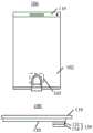
一种常见的应用场景,本申请实施例提供的指纹识别装置可以应用在智能手机、平板电脑以及其他具有显示屏的移动终端或者其他终端设备;更具体地,在上述终端设备中,指纹识别装置可以具体为光学指纹装置,其可以设置在显示屏下方的局部区域或者全部区域从而形成屏下(Under-display)光学指纹系统。A common application scenario, the fingerprint identification device provided by the embodiment of the present application can be applied to smart phones, tablet computers and other mobile terminals with display screens or other terminal devices; more specifically, in the above terminal devices, the fingerprint identification device It may specifically be an optical fingerprint device, which may be arranged in a partial or entire area under the display screen to form an under-display optical fingerprint system.
如图1所示为本申请实施例可以适用的终端设备的结构示意图,所述终端设备100包括显示屏120和指纹识别装置130,其中,所述指纹识别装置130设置在所述显示屏120下方的局部区域。所述指纹识别装置130可以包括具有多个光学感应单元的感应阵列,其中,所述感应阵列也可以是一个指纹传感器。所述感应阵列所在区域或者其光学感应区域为所述指纹识别装置130的指纹检测区域103。如图1所示,所述指纹检测区域103位于所述显示屏120的显示区域102之中,因此,使用者在需要对所述终端设备100进行解锁或者其他指纹验证的时候,只需要将手指按压在位于所述显示屏120的指纹检测区域103,便可以实现指纹输入。由于指纹检测可以在屏内实现,因此采用上述结构的终端设备100无需其正面专门预留空间来设置指纹按键(比如Home键)。As shown in FIG. 1 , it is a schematic structural diagram of a terminal device applicable to the embodiment of the present application. The
作为一种优选的实施例,所述显示屏120可以采用具有自发光显示单元的显示屏,比如有机发光二极管(Organic Light-Emitting Diode,OLED)显示屏或者微型发光二极管(Micro-LED)显示屏。另外,所述显示屏120可以具体为触控显示屏,其不仅可以进行画面显示,还可以检测用户的触摸或者按压操作,从而为用户提供一个人机交互界面。比如,在一种实施例中,所述终端设备100可以包括触摸控制器,所述触摸控制器可以具体为触控面板,其可以设置在所述显示屏120表面,也可以部分集成或者整体集成到所述显示屏120内部,从而形成所述触控显示屏。以采用OLED显示屏为例,所述指纹识别装置130可以利用所述OLED显示屏120位于所述指纹检测区域103的显示单元(即OLED光源)来作为光学指纹检测的激励光源。As a preferred embodiment, the
在其他实施例中,所述指纹识别装置130也可以采用内置光源或者外置光源来提供用于进行指纹检测的光信号。在这种情况下,所述指纹识别装置130可以适用于非自发光显示屏,比如液晶显示屏或者其他的被动发光显示屏。以应用在具有背光模组和液晶面板的液晶显示屏为例,为支持液晶显示屏的屏下指纹检测,所述指纹识别装置130还可以包括用于光学指纹检测的激励光源,所述激励光源可以具体为红外光源或者特定波长非可见光的光源,其可以设置在所述液晶显示屏的背光模组下方或者设置在所述终端设备100的保护盖板下方的边缘区域,而所述指纹识别装置130设置在所述背光模组下方,且所述背光模组通过对扩散片、增亮片、反射片等膜层进行开孔或者其他光学设计以允许指纹检测光穿过液晶面板和背光模组并到达所述指纹识别装置130的感应阵列。In other embodiments, the fingerprint identification device 130 may also use a built-in light source or an external light source to provide optical signals for fingerprint detection. In this case, the fingerprint identification device 130 can be applied to a non-self-luminous display screen, such as a liquid crystal display screen or other passive luminous display screens. Taking a liquid crystal display with a backlight module and a liquid crystal panel as an example, in order to support the under-screen fingerprint detection of the liquid crystal display, the fingerprint identification device 130 may also include an excitation light source for optical fingerprint detection, the excitation light source It can be specifically an infrared light source or a light source of non-visible light of a specific wavelength, which can be arranged under the backlight module of the liquid crystal display or in the edge area under the protective cover of the
并且,所述指纹识别装置130的感应阵列具体可以为光探测器(Photo detector)阵列,其包括多个呈阵列式分布的光探测器,所述光探测器可以作为如上所述的光学感应单元。当手指按压在所述指纹检测区域103时,所述指纹检测区域103的显示单元发出的光线在手指表面的指纹发生反射并形成反射光,其中所述手指指纹的脊和谷的反射光是不同的,反射光从所述显示屏120透过并被所述光探测器阵列所接收并转换为相应的电信号,即指纹检测信号;基于所述指纹检测信号便可以获得指纹图像数据,并且可以进一步进行指纹匹配验证,从而在所述终端设备100实现光学指纹识别功能。In addition, the sensing array of the fingerprint identification device 130 may specifically be a photo detector (Photo detector) array, which includes a plurality of photo detectors distributed in an array, and the photo detector may serve as the optical sensing unit as described above. . When a finger is pressed on the
在其他替代实施例中,所述指纹识别装置130也可以设置在所述显示屏120下方的整个区域,从而将所述指纹检测区域103扩展到整个所述显示屏120的整个显示区域102,实现全屏指纹识别。In other alternative embodiments, the fingerprint identification device 130 can also be arranged in the entire area below the
应当理解的是,在具体实现上,所述终端设备100还可以包括透明保护盖板110,所述盖板110可以为玻璃盖板或者蓝宝石盖板,其设置于所述显示屏120的上方并覆盖所述终端设备100的正面。因此,本申请实施例中,所谓的手指按压在所述显示屏120实际上是指按压在所述显示屏120上方的盖板110或者覆盖所述盖板110的保护层表面。It should be understood that, in a specific implementation, the
作为一种可选的实现方式,如图1所示,所述指纹识别装置130可以包括光检测部分134和光学组件132,所述光检测部分134包括所述感应阵列以及与所述感应阵列电连接的读取电路及其他辅助电路,其可以在通过半导体工艺制作在一个芯片(Die);即所述光检测部分134可以制作在光学成像芯片或者图像传感芯片上。As an optional implementation, as shown in FIG. 1, the fingerprint identification device 130 may include a photodetection part 134 and an optical component 132, and the photodetection part 134 includes the sensing array and is electrically connected to the sensing array. The connected reading circuit and other auxiliary circuits can be fabricated on a single chip (Die) through a semiconductor process; that is, the light detection part 134 can be fabricated on an optical imaging chip or an image sensing chip.
所述光学组件132可以设置在所述光检测部分134的感应阵列的上方,所述光学组件132可以包括滤光层(Filter)、导光层以及其他光学元件;所述滤光层可以用于滤除穿透手指的环境光,而所述导光层主要用于将从手指表面反射回来的反射光导引(比如光学准直或者汇聚)至所述感应阵列进行光学检测。The optical assembly 132 can be arranged above the sensing array of the light detection part 134, and the optical assembly 132 can include a filter layer (Filter), a light guide layer and other optical elements; the filter layer can be used for The ambient light penetrating the finger is filtered out, and the light guide layer is mainly used to guide (for example, optically collimate or converge) the reflected light reflected from the surface of the finger to the sensing array for optical detection.
所述显示屏120发出的光线在所述显示屏120上方的待检测手指表面发生反射,从手指反射回来的反射光经微孔阵列或者微透镜阵列进行光学准直或者汇聚之后,进一步经过滤光层的滤波后被所述光检测部分134接收,所述光检测部分134可以进一步对接收到的该反射光进行检测,从而获取到所述手指的指纹图像以实现指纹识别。The light emitted by the
应当理解,上述指纹识别装置130仅是一种示例性的结构,在具体实现上,该光学组件132的滤光层的位置并不局限在所述导光层的下方;比如,在一种替代实施例中,该滤光层也可以设置在所述导光层和所述显示屏120之间,即位于所述导光层上方;或者,所述光学组件132可以包括两层滤光层,二者分别设置在所述导光层的上方和下方。在其他替代实施例中,该滤光层也可以集成到所述导光层内部,甚至也可以省略掉,本申请对此不做限制。It should be understood that the above-mentioned fingerprint identification device 130 is only an exemplary structure, and in specific implementation, the position of the filter layer of the optical component 132 is not limited to be below the light guide layer; for example, in an alternative In an embodiment, the filter layer may also be disposed between the light guide layer and the
在具体实现上,所述光学组件132可以与所述光检测部分134封装在同一个光学指纹芯片。也可以是作为与光检测部分134相对独立的部件安装在指纹识别装置内部,即是将所述光学组件132设置在所述光检测部分134所在的芯片外部,比如将所述光学组件132贴合在所述芯片上方,或者将所述光学组件132的部分元件集成在上述芯片之中。其中,所述光学组件132的导光层有多种实现方案。In a specific implementation, the optical component 132 and the light detection part 134 may be packaged in the same optical fingerprint chip. It can also be installed inside the fingerprint identification device as a component relatively independent from the light detection part 134, that is, the optical component 132 is arranged outside the chip where the light detection part 134 is located, such as bonding the optical component 132 On the chip, or integrate some components of the optical component 132 into the chip. Wherein, the light guide layer of the optical component 132 has various implementation schemes.
在一种实施例中,所述光学组件132的导光层具体为在半导体硅片或者其他基材(比如硅氧化物或氮化物)制作而成的光路调制器或者光路准直器,其具有多个光路调制单元或者准直单元,具体地,所述光路调制单元或者准直单元可以具体为具有高深宽比的通孔,因此所述多个准直单元或者透镜单元可以构成通孔阵列。在从手指反射回来的反射光中,入射到所述光路调制单元或者准直单元的光线可以穿过并被其下方的光学感应单元接收,每一个光学感应单元基本上能够接收到其上方的通孔导引过来的指纹纹路的反射光,从而所述感应阵列便可以检测出手指的指纹图像。In one embodiment, the light guide layer of the optical component 132 is specifically an optical path modulator or an optical path collimator made on a semiconductor silicon wafer or other substrates (such as silicon oxide or nitride), which has A plurality of optical path modulation units or collimation units, specifically, the optical path modulation units or collimation units may specifically be through holes with a high aspect ratio, so the plurality of collimation units or lens units may form a through hole array. In the reflected light reflected from the finger, the light incident on the optical path modulation unit or the collimation unit can pass through and be received by the optical sensing unit below it, and each optical sensing unit can basically receive the passing light above it. The reflected light of the fingerprint pattern guided by the holes, so that the sensing array can detect the fingerprint image of the finger.
在其他替代实施例中,所述导光层也可以包括光学透镜(Lens)层,其具有一个或多个光学透镜单元,比如一个或多个非球面型微透镜组成的透镜组。从手指反射回来的反射光经所述光学透镜单元进行光路准直或者汇聚之后,并被其下方的光学感应单元接收,据此,所述感应阵列可以检测出手指的指纹图像。In other alternative embodiments, the light guide layer may also include an optical lens (Lens) layer, which has one or more optical lens units, such as a lens group composed of one or more aspherical micro-lenses. The reflected light reflected from the finger is collimated or converged by the optical lens unit, and then received by the optical sensing unit below it, so that the sensing array can detect the fingerprint image of the finger.
另一方面,所述光检测部分134的感应阵列可以具体只包括单一的感应阵列,也可以采用具有两个或以上并排设置的感应阵列的双感应阵列(Dual Array)或多感应阵列(Multiple Array)的架构。当所述光检测部分134采用双感应阵列或者多感应阵列架构时,所述光学组件132可以采用单独一个导光层同时覆盖所述两个或以上的感应阵列;可替代地,所述光学组件132也可以包括两个或以上并排设置的导光层,比如两个或以上的光路调制器或光路准直器,或者两个或以上的光学透镜层,所述两个或以上并排设置的导光层分别对应设置在所述两个或以上的感应阵列的上方,用于将相关反射光导引或者汇聚到其下方的感应阵列。On the other hand, the sensing array of the light detection part 134 may specifically only include a single sensing array, or a dual sensing array (Dual Array) or a multiple sensing array (Multiple Array) with two or more sensing arrays arranged side by side may also be used. ) structure. When the light detection part 134 adopts a dual sensing array or multi-sensing array structure, the optical assembly 132 can use a single light guide layer to cover the two or more sensing arrays at the same time; alternatively, the optical assembly 132 may also include two or more light guide layers arranged side by side, such as two or more optical path modulators or optical path collimators, or two or more optical lens layers, and the two or more light guide layers arranged side by side The optical layers are correspondingly disposed above the two or more sensing arrays, and are used to guide or converge related reflected light to the sensing arrays below them.
在其他替代实现方式中,所述显示屏120也可以采用非自发光的显示屏,比如采用背光的液晶显示屏;在这种情况下,所述指纹识别装置130便无法采用所述显示屏120的显示单元作为激励光源,因此需要在所述指纹识别装置130内部集成激励光源或者在其外部设置激励光源来实现光学指纹检测,其检测原理与上面描述内容是一致的。In other alternative implementations, the
应当理解,虽然在图1所示的实施例中以所述指纹识别装置为屏下光学指纹识别装置为例,但是,在其他实施例中,所述终端设备100的指纹识别装置也可以采用超声波指纹识别装置或者其他类型的指纹识别装置代替。本申请对指纹识别装置的类型和具体结构不作特殊限制,只要上述指纹识别装置可以满足在终端设备的显示屏内部进行指纹识别的性能要求便可。It should be understood that although in the embodiment shown in FIG. 1 the fingerprint recognition device is an under-screen optical fingerprint recognition device as an example, in other embodiments, the fingerprint recognition device of the
在一种实现方式中,指纹识别装置130可以采用周期性微孔阵列将光线传输到感应阵列上,这种方案光能量损失大,传感器曝光时间长。In an implementation manner, the fingerprint recognition device 130 may use a periodic microhole array to transmit light to the sensing array. This solution has a large loss of light energy and a long exposure time of the sensor.
在另一种实现方式中,指纹识别装置130可以采用微透镜将光线传输到感应阵列上,并且由于采用的是普通的透镜,在成像过程中,当物距发生变化时,其所成图像大小会相应的发生变化,可能会导致同一个焦距的镜头,对应不同的物距,将会有不同的放大倍率。另外,普通镜头都存在一定范围的景深,当被测物体不在镜头的景深范围内时图像就会变得模糊,无法清晰聚焦。从而导致指纹识别精度不高。In another implementation, the fingerprint recognition device 130 can use microlenses to transmit light to the sensing array, and because ordinary lenses are used, when the object distance changes during the imaging process, the size of the formed image will It will change accordingly, which may cause a lens with the same focal length to have different magnifications corresponding to different object distances. In addition, ordinary lenses have a certain depth of field. When the measured object is not within the depth of field of the lens, the image will become blurred and cannot be clearly focused. As a result, the fingerprint recognition accuracy is not high.
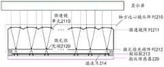
为了解决上述各种问题,本申请实施例提供了一种新的指纹识别装置,该指纹识别装置可以设置在显示屏下方。具体地,如图2所示,该指纹识别装置200可以包括物方远心镜头阵列210和指纹传感器220,所述物方远心镜头阵列210用于接收经由人体手指反射形成光信号,进而对该光信号进行准直和聚焦。所述指纹传感器220设置于所述物方远心镜头阵列210的下方,并且与所述物方远心镜头阵列210采用可分离式装配结构,所述指纹传感器220用于基于穿过所述物方远心镜头阵列210的所述光信号进行成像。所述可分离式装配结构方便将指纹传感器220和物方远心镜头阵列210进行组装和拆卸,可以灵活调整上述两者之间的距离,进而可以得到比直接在指纹传感器表面生长微透镜阵列的方案更好的准直性和成像质量。本申请实施例采用框贴工艺来实现所述可分离式装配结构,具体参见图5及其内容描述。所述可分离式装配结构还可以通过其他方式实现,比如机械固定方式,只要能够方便组装和拆卸,灵活调整指纹传感器220和物方远心镜头阵列210之间的距离即可,本申请实施例不做限定。为了便于理解,首先对远心镜头做一个简单的介绍。In order to solve the various problems above, the embodiment of the present application provides a new fingerprint identification device, which can be arranged under the display screen. Specifically, as shown in FIG. 2 , the fingerprint identification device 200 may include an object-space telecentric lens array 210 and a fingerprint sensor 220, and the object-space telecentric lens array 210 is used to receive light signals formed by reflection of human fingers, and then to The optical signal is collimated and focused. The fingerprint sensor 220 is arranged below the object-space telecentric lens array 210, and adopts a detachable assembly structure with the object-space telecentric lens array 210. The fingerprint sensor 220 is used for The optical signal of the square telecentric lens array 210 is imaged. The detachable assembly structure facilitates the assembly and disassembly of the fingerprint sensor 220 and the object-space telecentric lens array 210, and can flexibly adjust the distance between the two, and then can obtain a microlens array that is better than directly growing a microlens array on the surface of the fingerprint sensor. Program for better collimation and imaging quality. The embodiment of the present application adopts the frame-attaching process to realize the detachable assembly structure, see FIG. 5 and its content description for details. The detachable assembly structure can also be realized in other ways, such as mechanical fixing, as long as it can be easily assembled and disassembled, and the distance between the fingerprint sensor 220 and the object-space telecentric lens array 210 can be flexibly adjusted. No limit. For ease of understanding, a brief introduction to the telecentric lens is given first.
所谓远心镜头,实质为普通镜头与小孔成像原理的结合。其可以在一定的物距范围内,使得到的图像放大倍率不会变化,不随景深变化而变化,并且无视差,将其应用于指纹识别技术中,可以提高指纹识别的精度。The so-called telecentric lens is essentially a combination of ordinary lens and pinhole imaging principle. It can keep the magnification of the obtained image unchanged within a certain range of object distance, does not change with the depth of field, and has no parallax. Applying it to fingerprint identification technology can improve the accuracy of fingerprint identification.
通常,远心镜头又可以分为物方远心镜头、像方远心镜头和双远心镜头。下面结合图3来主要说明物方远心镜头的原理。Generally, telecentric lenses can be divided into object-space telecentric lenses, image-space telecentric lenses, and bi-telecentric lenses. The principle of the object-space telecentric lens will be mainly described below in conjunction with FIG. 3 .
图3示出了物方远心镜头的成像原理。如图3所示,在普通透镜的像方焦平面处放置孔径光阑,这个孔径光阑的作用是只让平行入射的物方光线(如光线1和光线2)可以到达像平面成像,从几何关系可以看出这时像没有近大远小的关系了。也就是说,相当于物体在无穷远处。Figure 3 shows the imaging principle of the object-space telecentric lens. As shown in Figure 3, an aperture stop is placed at the focal plane of the image space of a common lens. The function of this aperture stop is to allow only parallel incident light rays from the object space (such as light 1 and light 2) to reach the image plane for imaging. From the geometric relationship, it can be seen that there seems to be no relationship between near, large, and far. That is to say, it is equivalent to an object at infinity.
由于单个远心镜头进行成像,通常需要比较大的成像面,因此整个透镜组会比较厚。但是将远心镜头阵列化微型化之后,就可以对一定距离的物体成像,从而可以应用于指纹识别技术中。而阵列化微型化之后的物方远心镜头即构成本申请实施例提供的指纹识别装置200中的物方远心镜头阵列210。Since a single telecentric lens usually needs a relatively large imaging surface for imaging, the entire lens group will be relatively thick. However, after the telecentric lens array is miniaturized, it can image objects at a certain distance, which can be applied to fingerprint recognition technology. The object-space telecentric lens after arraying and miniaturization constitutes the object-space telecentric lens array 210 in the fingerprint identification device 200 provided in the embodiment of the present application.
如图4所示,物方远心镜头阵列210可以包括微透镜阵列211和微孔径光阑阵列212。可选地,微透镜阵列211可以包括多个微透镜单元,所述微透镜单元包括一片或多片微透镜,当所述微透镜单元包括多片所述微透镜时,多片所述微透镜的主光轴和焦点均重合。As shown in FIG. 4 , the object-space telecentric lens array 210 may include a microlens array 211 and a micro-aperture stop array 212 . Optionally, the microlens array 211 may include a plurality of microlens units, and the microlens unit includes one or more microlenses. When the microlens unit includes multiple microlenses, the multiple microlenses The principal optical axis and focal point of both coincide.
微孔径光阑阵列212,设置于微透镜阵列211的下方并且位于所述微透镜单元的像方焦平面处,所述微孔径光阑阵列212包括多个微孔径光阑,所述微透镜单元与所述微孔径光阑一一对应。The micro-aperture diaphragm array 212 is arranged below the micro-lens array 211 and is positioned at the focal plane of the image side of the micro-lens unit, the micro-aperture diaphragm array 212 includes a plurality of micro-aperture diaphragms, and the micro-lens unit correspond to the micro-aperture diaphragms one by one.
在本申请实施例中,指纹传感器220的一个像素单元对应至少一个所述微透镜单元。可替代地,可以将指纹传感器220的一个像素单元对应四个所述微透镜单元,以提高指纹传感器220的像素阵列密度。In the embodiment of the present application, one pixel unit of the fingerprint sensor 220 corresponds to at least one microlens unit. Alternatively, one pixel unit of the fingerprint sensor 220 may correspond to four microlens units, so as to increase the pixel array density of the fingerprint sensor 220 .
作为一种可选的实施例,微透镜阵列211与微孔径光阑阵列212可以加工到同一基底材料的两个表面上,可以减少工艺步骤。即微透镜阵列211与微孔径光阑阵列212位于同一透明基底的正、反两个表面,可选地,所述透明基底为玻璃或者塑料。As an optional embodiment, the micro-lens array 211 and the micro-aperture stop array 212 can be processed on two surfaces of the same base material, which can reduce process steps. That is, the microlens array 211 and the microaperture stop array 212 are located on the front and back surfaces of the same transparent substrate, and optionally, the transparent substrate is glass or plastic.
作为另一种可选的实施例,微透镜阵列211与微孔径光阑阵列212可以分别位于不同基底上,之后再将微孔径光阑阵列212设置于微透镜阵列211的下方。可选地,微透镜阵列211所在的基底可以为透明基底,例如玻璃或者塑料,微孔径光阑阵列212所在的基底可以为透明基底,也可以为其他非透明基底材料,本实施例不做限定。可选地,微透镜阵列211与微孔径光阑阵列212之间可以通过以下任一透明介质或以下透明介质的任意组合填充:空气、玻璃和塑料。As another optional embodiment, the microlens array 211 and the microaperture stop array 212 may be respectively located on different substrates, and then the microaperture stop array 212 is disposed under the microlens array 211 . Optionally, the substrate where the microlens array 211 is located can be a transparent substrate, such as glass or plastic, and the substrate where the micro-aperture stop array 212 is located can be a transparent substrate or other non-transparent substrate material, which is not limited in this embodiment . Optionally, the space between the micro-lens array 211 and the micro-aperture stop array 212 may be filled with any of the following transparent media or any combination of the following transparent media: air, glass and plastic.
可选地,本申请实施例中的微透镜可以采用微纳加工工艺或压模工艺实现,而本申请实施例中的微孔径光阑可以通过微纳加工工艺或纳米印制工艺来制作,进而可以实现将物方远心镜头微型化阵列化。Optionally, the microlens in the embodiment of the present application can be realized by using a micro-nano-fabrication process or a compression molding process, and the micro-aperture diaphragm in the embodiment of the present application can be produced by a micro-nano-fabrication process or a nano-printing process, and then It can realize the miniaturization and arraying of the object-space telecentric lens.
对于阵列化的物方远心镜头,单个像素周期需与物体的分辨率需求相关,例如设置于显示屏下的指纹识别装置,可以将远心镜头的像素周期设置为沿显示屏的平面X/Y方向各为25μm采样率。For an arrayed object-space telecentric lens, the single pixel period needs to be related to the resolution requirements of the object. For example, for a fingerprint recognition device installed under the display screen, the pixel period of the telecentric lens can be set to be along the plane X/ The sampling rate is 25 μm each in the Y direction.
本申请实施例提供的指纹识别装置,采用物方远心镜头,能够对远心镜头上方区域进行指纹采集,并将上方区域的光聚焦到指纹传感器的像素单元。并且通过将远心镜头微型化和阵列化,可以实现在一定距离内的指纹成像。相对于周期性通孔阵列的方案来说,可以避免垂直方向的光损失,进而可以减少指纹传感器的曝光时间。相对于微透镜的方案,该指纹识别装置也能让整个系统的成像畸变减小,该指纹识别装置可以达到较高的成像质量以及对比度。The fingerprint recognition device provided by the embodiment of the present application adopts an object-space telecentric lens, which can collect fingerprints on the area above the telecentric lens, and focus the light in the upper area to the pixel unit of the fingerprint sensor. And by miniaturizing and arraying the telecentric lens, fingerprint imaging within a certain distance can be realized. Compared with the solution of the periodic through-hole array, the light loss in the vertical direction can be avoided, thereby reducing the exposure time of the fingerprint sensor. Compared with the solution of the microlens, the fingerprint identification device can also reduce the imaging distortion of the whole system, and the fingerprint identification device can achieve higher imaging quality and contrast.
可选地,本申请实施例中,所述微透镜单元中的所述微透镜的占空比的范围可以为50%~100%,所述微透镜的球冠可以为球面或者非球面,所述微透镜的焦距范围可以为10μm~2000μm。可选地,所述微孔径光阑的直径范围可以为1μm~10μm。Optionally, in this embodiment of the present application, the duty ratio of the microlens in the microlens unit may range from 50% to 100%, and the spherical cap of the microlens may be spherical or aspheric, so The focal length of the microlens may range from 10 μm to 2000 μm. Optionally, the diameter of the micro-aperture stop may range from 1 μm to 10 μm.
图5示出了本申请实施例的指纹识别装置的结构性示意图。当指纹识别装置200应用于具有显示屏的电子设备时,指纹识别装置200固定于所述显示屏的下方,且与所述显示屏之间存在间隙。当所述电子设备包括中框时,指纹识别装置200还可以固定于所述中框上。FIG. 5 shows a schematic structural diagram of a fingerprint recognition device according to an embodiment of the present application. When the fingerprint identification device 200 is applied to an electronic device with a display screen, the fingerprint identification device 200 is fixed below the display screen, and there is a gap between the fingerprint identification device 200 and the display screen. When the electronic device includes a middle frame, the fingerprint identification device 200 may also be fixed on the middle frame.
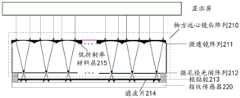
如图2所介绍的内容,指纹识别装置200除了可以包括物方远心镜头阵列210,指纹传感器220之外,可选地,指纹识别装置200还可以包括滤波片214,用于对由人体手指反射形成的所述光信号进行过滤。滤波片214可以设置在指纹传感器220的上方和所述显示屏之间,例如,如图5所示,滤波片214可以设置在物方远心镜头阵列210和指纹传感器220之间。可选地,滤波片214还可以通过生长工艺,直接生长在所述指纹传感器220的表面。As shown in Figure 2, in addition to the object-space telecentric lens array 210 and the fingerprint sensor 220, the fingerprint identification device 200 may optionally include a filter 214 for detecting The optical signal formed by reflection is filtered. The filter 214 may be disposed above the fingerprint sensor 220 and between the display screen, for example, as shown in FIG. 5 , the filter 214 may be disposed between the object-space telecentric lens array 210 and the fingerprint sensor 220 . Optionally, the filter 214 can also be directly grown on the surface of the fingerprint sensor 220 through a growth process.
应理解,在具体实现上,滤波片214的位置并不局限在物方远心镜头阵列210和指纹传感器220之间,也可以设置在物方远心镜头阵列210和所述显示屏之间,即位于所述物方远心镜头阵列210的上方,可选地,滤波片214可以通过生长工艺直接生长在物方远心镜头阵列210的上表面。作为一种可选的实施例,指纹识别装置200还可以包括两层滤波片214,分别设置在物方远心镜头阵列210的上方和下方。It should be understood that, in specific implementation, the position of the filter 214 is not limited to between the object-space telecentric lens array 210 and the fingerprint sensor 220, and may also be arranged between the object-space telecentric lens array 210 and the display screen, That is, it is located above the object-space telecentric lens array 210 , optionally, the filter 214 can be directly grown on the upper surface of the object-space telecentric lens array 210 through a growth process. As an optional embodiment, the fingerprint identification device 200 may also include two layers of filters 214, which are respectively arranged above and below the object-space telecentric lens array 210.
在其他可替代的实施例当中,滤波片214不限于采用生长工艺进行设置,也可以通过其他工艺设置在指纹传感器220的上方,比如蒸镀工艺,本实施例不做限定。In other alternative embodiments, the filter 214 is not limited to be disposed by a growth process, and may also be disposed above the fingerprint sensor 220 by other processes, such as an evaporation process, which is not limited in this embodiment.
应理解,滤波片可以用来减少指纹感应中的不期望的背景光,以提高指纹传感器对接收到的光的光学感应。该滤波片具体可以用于过滤掉环境光波长,例如,近红外光和部分的红光等。又例如,蓝光或者部分蓝光。例如,人类手指吸收波长低于580nm的光的能量中的大部分,如果一个或多个光学过滤器或光学过滤涂层可以设计为过滤波长从580nm至红外的光,则可以大大减少环境光对指纹感应中的光学检测的影响。It should be understood that filters may be used to reduce unwanted background light in fingerprint sensing to improve the optical sensitivity of the fingerprint sensor to received light. The filter can be specifically used to filter out wavelengths of ambient light, for example, near-infrared light and part of red light. Another example is Blu-ray or part of Blu-ray. For example, human fingers absorb most of the energy of light with wavelengths below 580nm, if one or more optical filters or optical filter coatings can be designed to filter light from 580nm to infrared wavelengths, the impact of ambient light on Impact of optical detection in fingerprint sensing.
可选地,该滤波片214可以为红外截止光学滤波片。Optionally, the filter 214 may be an infrared cut optical filter.
在图2具体描述内容当中,已经介绍了指纹传感器220和物方远心镜头阵列210采用可分离式装配结构,图5当中的实施例示出了采用框贴工艺来实现所述可分离式装配结构。具体地,指纹传感器220和物方远心镜头阵列210之间通过框贴胶213将四边进行固定,框贴胶213可以是超薄双面胶,也可以是其他具有粘合性质的粘合剂,只要能够将指纹传感器220和物方远心镜头阵列210进行框贴固定即可,本实施例不做限定。In the specific description of FIG. 2, it has been introduced that the fingerprint sensor 220 and the object-space telecentric lens array 210 adopt a detachable assembly structure, and the embodiment in FIG. 5 shows that the detachable assembly structure is realized by using a frame sticking process. . Specifically, between the fingerprint sensor 220 and the object-space telecentric lens array 210, the four sides are fixed by the frame adhesive 213. The frame adhesive 213 can be an ultra-thin double-sided adhesive, or other adhesives with adhesive properties. , as long as the fingerprint sensor 220 and the object-space telecentric lens array 210 can be frame-mounted and fixed, it is not limited in this embodiment.
图4当中已经介绍过,物方远心镜头阵列210可以包括微透镜阵列211和微孔径光阑阵列212,图5当中示出了一种可选的实施例,即微透镜阵列211与微孔径光阑阵列212位于同一透明基底的正、反两个表面。同时,本实施例还示出了微孔径光阑阵列212位于微透镜单元2110的像方焦平面处,并且微孔径光阑2120设置于微透镜单元2110的焦点处,因此物方远心镜头阵列210可以导引平行于微透镜单元2110的主光轴方向的光信号通过。可选地,微孔径光阑2120还可以偏离于微透镜单元的2110的主光轴设置,此时,物方远心镜头阵列210可以导引倾斜于微透镜单元2110的主光轴方向的特定角度的光信号通过,这里微孔径光阑2120偏离于所述微透镜单元2110的主光轴的距离的范围可以为0μm~50μm,可选地,将微孔径光阑2120偏离于所述微透镜单元2110的主光轴5μm处设置。It has been introduced among Fig. 4 that the object-space telecentric lens array 210 may include a microlens array 211 and a microaperture diaphragm array 212. An optional embodiment is shown in Fig. 5, that is, the microlens array 211 and the microaperture stop array 212 The aperture array 212 is located on the front and back surfaces of the same transparent substrate. At the same time, the present embodiment also shows that the micro-aperture stop array 212 is located at the focal plane of the image side of the micro-lens unit 2110, and the micro-aperture stop 2120 is arranged at the focal point of the micro-lens unit 2110, so the object-side telecentric lens array 210 may guide an optical signal in a direction parallel to the main optical axis of the microlens unit 2110 to pass. Optionally, the micro-aperture stop 2120 can also be deviated from the main optical axis of the microlens unit 2110. At this time, the object-space telecentric lens array 210 can guide a specific The optical signal of the angle passes through. Here, the distance between the micro-aperture stop 2120 and the main optical axis of the microlens unit 2110 can range from 0 μm to 50 μm. Optionally, the micro-aperture stop 2120 is deviated from the microlens The principal optical axis of cell 2110 is set at 5 μm.
可选地,在本申请实施例中,物方远心镜头阵列210的材质可以是玻璃,也可以是塑料,还可以是其他透明质材料。另外,该微透镜阵列211的排列方式可以是正方形排列,也可以是六边形排列,还可以是其他任意形式,本申请实施例对此不构成限定。当微透镜阵列211采用正方形排列方式时,所述微透镜的占空比可以高达100%。Optionally, in the embodiment of the present application, the material of the object-space telecentric lens array 210 may be glass, plastic, or other transparent materials. In addition, the arrangement of the microlens array 211 may be a square arrangement, a hexagonal arrangement, or any other form, which is not limited by this embodiment of the present application. When the microlens array 211 adopts a square arrangement, the duty cycle of the microlenses can be as high as 100%.
可选地,如图6所示,物方远心镜头阵列210还可以包括低折射率材料层215,低折射率材料层215设置在微透镜阵列211的上方,用于填平并保护微透镜阵列211,并且仍然保证所述微透镜单元2110的像方焦平面与微孔径光阑阵列212重合。采用低折射率材料层215填平微透镜阵列211的表面,使得整个指纹识别装置200应用到电子设备或者其他设备时更加易于安装。可选地,可以采用生长、涂覆、浸泡、蒸镀等工艺或者其他工艺将低折射率材料层215设置于微透镜阵列211的上方,本实施例不做限定。可以理解的是,当微透镜阵列211的上方设置有低折射率材料层215时,滤波片214设置于物方远心镜头阵列210的表面其实质为滤波片214设置于所述低折射率材料层215的表面。Optionally, as shown in FIG. 6 , the object-space telecentric lens array 210 may also include a low-refractive-
需要注意的是,图6所示出的低折射率材料层215只是示意性的,低折射率材料层215填平微透镜阵列211后,还可以具有一定的厚度,所述厚度依据实际情况而设定,本实施例不做限定。It should be noted that the low-refractive
图7为本申请实施例的另一种指纹识别装置的结构性示意图。与图6所示出的指纹识别装置不同的是,图7当中,透明基底内包括两层遮光层216,即所述遮光层216位于微透镜阵列211和微孔径光阑阵列212之间。可选地,所述透明基底当中还可以只包括一层遮光层216或者包括多层遮光层216。遮光层216被设置为允许来自所述微透镜单元2110上方的所述光信号通过,每一层遮光层216当中均包括多个通光孔,并且所述通光孔与所述微透镜单元一一对应。可选地,如图7所示,位于上层的遮光层216的通光孔的直径大于位于下层的遮光层216的通光孔的直径。可选地,这里所述通光孔的中心位于微透镜单元2110的主光轴上。因此物方远心镜头阵列210可以导引平行于微透镜单元2110的主光轴方向的光信号通过。通过在透明基底中设置遮光层216,可以减少环境光、杂散光等对于指纹检测的干扰,还可以减少相邻微透镜单元2110之间所述光信号的串扰,进一步得到更好的成像质量和效果。FIG. 7 is a structural schematic diagram of another fingerprint recognition device according to an embodiment of the present application. Different from the fingerprint identification device shown in FIG. 6 , in FIG. 7 , the transparent substrate includes two layers of light-shielding layers 216 , that is, the light-shielding layers 216 are located between the microlens array 211 and the micro-aperture stop array 212 . Optionally, the transparent substrate may include only one light-shielding layer 216 or multiple light-shielding layers 216 . The light-shielding layer 216 is set to allow the light signal from above the micro-lens unit 2110 to pass through, and each layer of light-shielding layer 216 includes a plurality of light-through holes, and the light-through holes are the same as the micro-lens unit One to one correspondence. Optionally, as shown in FIG. 7 , the diameter of the light hole of the upper light shielding layer 216 is larger than the diameter of the light hole of the lower light shielding layer 216 . Optionally, the center of the light through hole is located on the main optical axis of the microlens unit 2110 . Therefore, the object-space telecentric lens array 210 can guide light signals parallel to the main optical axis of the microlens unit 2110 to pass through. By setting the light-shielding layer 216 in the transparent substrate, the interference of ambient light, stray light, etc. on the fingerprint detection can be reduced, and the crosstalk of the optical signal between adjacent microlens units 2110 can be reduced, and better imaging quality and Effect.
作为一种可选的实施例,遮光层216的通光孔还可以与所述微孔径光阑一起偏离于所述微透镜单元2110的主光轴设置,使得物方远心镜头阵列210可以导引倾斜于微透镜单元2110的主光轴方向的特定角度的光信号通过,As an optional embodiment, the light-through hole of the light-shielding layer 216 can also be set away from the main optical axis of the microlens unit 2110 together with the micro-aperture stop, so that the object-side telecentric lens array 210 can guide The optical signal inclined to the specific angle of the main optical axis direction of the microlens unit 2110 passes through,
图8示出了本申请实施例提供的指纹识别装置的示意性结构图。当该指纹识别装置应用于电子设备(例如智能手机)时,如图8所示,保护盖板310的下表面与显示屏320的上表面贴合,该指纹识别装置330可以固定设置在该显示屏320的下方,该指纹识别装置330的下表面与柔性电路板350进行焊接固定。并且该指纹识别装置330与该显示屏320之间存在间隙390。作为一种可选地实现方式,该指纹识别装置330可以通过固定连接在电子设备内部容易拆卸的器件上来实现安装在该显示屏320的下方,例如可以将指纹识别装置330安装在中框370的下表面,该中框370可以作为该指纹识别装置330与该显示屏320之间的固定架,该中框370的上表面可以与该显示屏320的下表面边缘部分通过泡棉背胶360贴合。该中框370设置于显示屏320和后盖中间并用于承载内部各种组件的框架,其内部各种组件包括但不限于电池,主板,摄像头,排线,各种感应器,话筒,听筒等等零部件。由此,使得该指纹识别装置330和该显示屏320完全解耦,避免了安装或者拆卸该指纹识别装置330时损坏该显示屏320。FIG. 8 shows a schematic structural diagram of a fingerprint recognition device provided by an embodiment of the present application. When the fingerprint identification device is applied to an electronic device (such as a smart phone), as shown in FIG. Below the
可替代地,该指纹识别装置330也可以安装在显示屏320和中框370之间,并且与显示屏320之间具有间隙。例如,可以将指纹识别装置330安装在中框370的上表面。从而不需避让电子设备内部的各种零部件,例如,该指纹识别装置330与电池在电子设备的厚度方向上可以重合,使得指纹识别装置的摆放位置不再受限。Alternatively, the
可选地,该指纹识别装置330与显示屏320下方的距离可以大于或等于20μm。满足指纹识别装置330与显示屏320安装的安全距离,不会因振动或者跌落而造成器件损失。Optionally, the distance between the
该中框370具体可以由金属或者合金材料制成,甚至可以由塑胶材料制成,这种情况下,该中框370甚至可以和电子设备的边框一体成型,所谓一体成型就是内部中框和边框是一个整体。比如,边框可以只是一个金属贴边,或者可以在中框上面镀一层类似金属的涂料。进一步地,该中框370还可以是复合中框,以手机为例,中框370包括内中框1与外中框2,内中框1用于承载手机零部件,外中框2在内中框1外,外中框2外沿装有手机按键,内中框1与外中框2整合为一体。由于将手机中框设计成内中框与外中框,内外中框整合为一整体,手机受撞击时,首先是外中框磨损,由于外中框上只有按键,更换外中框简单方便,成本低;进一步地,可以在内外中框之间设置有弹性材料,由于内外中框在弹性层弹力的压紧下相对固定,因此,在外中框承受冲击力时弹性层可以减小对内中框的冲击。Specifically, the
可选地,在显示屏320的下方可以设置一层泡棉,在显示屏320下方与指纹识别装置330之间可以形成密闭环境,以此可以达到遮光、防尘的要求。而在指纹识别装置330的安装位置处可以将泡棉层开孔,使得指纹识别装置330能够接收到透过显示屏320的光信号。当手指放于点亮的显示屏320上方,手指就会反射显示屏320发出的光,此反射光会穿透显示屏320。指纹是一个漫反射体,其反射光在各方向都存在。使用特定光路,使指纹传感器只接收特定方向的光,通过算法可以解算出指纹。Optionally, a layer of foam can be arranged under the
本申请实施例还提供了一种电子设备,该电子设备包括上述各种实施例中的指纹识别装置和显示屏,该指纹识别装置位于显示屏的下方。进一步地,该电子设备还包括中框,该指纹识别装置可以固定于该中框上。The embodiment of the present application also provides an electronic device, the electronic device includes the fingerprint identification device and the display screen in the various embodiments above, and the fingerprint identification device is located below the display screen. Further, the electronic device also includes a middle frame, and the fingerprint identification device can be fixed on the middle frame.
图9是根据本申请实施例提供的电子设备400的示意性框图。图8所示的电子设备400包括:射频(Radio Frequency,RF)电路410、存储器420、其他输入设备430、显示屏440、传感器450、音频电路460、I/O子系统470、处理器480、以及电源490等部件。本领域技术人员可以理解,图7中示出的电子设备结构并不构成对电子设备的限定,可以包括比图示更多或更少的部件,或者组合某些部件,或者拆分某些部件,或者不同的部件布置。本领领域技术人员可以理解显示屏440属于用户界面(User Interface,UI),且电子设备400可以包括比图示或者更少的用户界面。Fig. 9 is a schematic block diagram of an
下面结合图9对电子设备400的各个构成部件进行具体的介绍:The components of the
RF电路410可用于收发信息或通话过程中,信号的接收和发送,特别地,将基站的下行信息接收后,给处理器480处理;另外,将设计上行的数据发送给基站。通常,RF电路包括但不限于天线、至少一个放大器、收发信机、耦合器、低噪声放大器(Low NoiseAmplifier,LNA)、双工器等。此外,RF电路410还可以通过无线通信与网络和其他设备通信。存储器420可用于存储软件程序以及模块,处理器480通过运行存储在存储器420的软件程序以及模块,从而执行电子设备400的各种功能应用以及数据处理。存储器420可主要包括存储程序区和存储数据区,其中,存储程序区可存储操作系统、至少一个功能所需的应用程序(比如声音播放功能、图像播放功能等)等;存储数据区可存储根据电子设备400的使用所创建的数据(比如音频数据、电话本等)等。此外,存储器420可以包括高速随机存取存储器,还可以包括非易失性存储器,例如至少一个磁盘存储器件、闪存器件、或其他易失性固态存储器件。The
其他输入设备430可用于接收输入的数字或字符信息,以及产生与电子设备400的用户设置以及功能控制有关的信号输入。具体地,其他输入设备430可包括但不限于物理键盘、功能键(比如音量控制按键、开关按键等)、轨迹球、鼠标、操作杆、光鼠(光鼠是不显示可视输出的触摸敏感表面,或者是由屏幕形成的触摸敏感表面的延伸)等中的一种或多种。其他输入设备430与I/O子系统470的其他输入设备控制器471相连接,在其他设备输入控制器471的控制下与处理器480进行信号交互。
显示屏440可用于显示由用户输入的信息或提供给用户的信息以及电子设备400的各种菜单,还可以接受用户输入。具体的显示屏440可以是触控屏,可包括显示面板441,以及触控面板442。触控面板442可覆盖显示面板441,用户可以根据显示面板441显示的内容(该显示内容包括但不限于,软键盘、虚拟鼠标、虚拟按键、图标等等),在显示面板441上覆盖的触控面板442上或者附近进行操作,触控面板442检测到在其上或附近的操作后,通过I/O子系统470传送给处理器480以确定用户输入,随后处理器480根据用户输入通过I/O子系统470在显示面板441上提供相应的视觉输出。虽然在图9中,触控面板442与显示面板441是作为两个独立的部件来实现电子设备400的输入和输入功能,但是在某些实施例中,可以将触控面板442与显示面板441集成而实现电子设备400的输入和输出功能。The
电子设备400还可包括至少一种传感器450,例如,该传感器450可以是位于显示屏440下或显示屏440内的指纹传感器,也就是本申请实施例中的指纹识别装置。The
音频电路460、扬声器461,麦克风462可提供用户与电子设备400之间的音频接口。音频电路460可将接收到的音频数据转换后的信号,传输到扬声器461,由扬声器461转换为声音信号输出;另一方面,麦克风462将收集的声音信号转换为信号,由音频电路460接收后转换为音频数据,再将音频数据输出至RF电路410以发送给比如另一手机,或者将音频数据输出至存储器420以便进一步处理。The
I/O子系统470用来控制输入输出的外部设备,可以包括其他设备输入控制器471、传感器控制器472、显示控制器473。可选的,一个或多个其他输入控制设备控制器471从其他输入设备430接收信号和/或者向其他输入设备430发送信号,其他输入设备430可以包括物理按钮(按压按钮、摇臂按钮等)、拨号盘、滑动开关、操纵杆、点击滚轮、光鼠(光鼠是不显示可视输出的触摸敏感表面,或者是由屏幕形成的触摸敏感表面的延伸)。值得说明的是,其他输入控制设备控制器471可以与任一个或者多个上述设备连接。所述I/O子系统470中的显示控制器473从显示屏440接收信号和/或者向显示屏440发送信号。显示屏440检测到用户输入后,显示控制器473将检测到的用户输入转换为与显示在显示屏440上的用户界面对象的交互,即实现人机交互。传感器控制器472可以从一个或者多个传感器440接收信号和/或者向一个或者多个传感器440发送信号。The I/
处理器480是电子设备400的控制中心,利用各种接口和线路连接整个电子设备的各个部分,通过运行或执行存储在存储器420内的软件程序和/或模块,以及调用存储在存储器420内的数据,执行电子设备400的各种功能和处理数据,从而对电子设备进行整体监控。可选的,处理器480可包括一个或多个处理单元;优选的,处理器480可集成应用处理器和调制解调处理器,其中,应用处理器主要处理操作系统、用户界面和应用程序等,调制解调处理器主要处理无线通信。可以理解的是,上述调制解调处理器也可以不集成到处理器480中。该处理器480可以用来执行本申请方法实施例中的各个步骤。The
电子设备400还包括给各个部件供电的电源490(比如电池),优选的,电源可以通过电源管理系统与处理器480逻辑相连,从而通过电源管理系统实现管理充电、放电、以及功耗等功能。The
尽管未示出,电子设备400还可以包括摄像头、蓝牙模块等,在此不再赘述。Although not shown, the
应理解,说明书通篇中提到的“一个实施例”或“一实施例”意味着与实施例有关的特定特征、结构或特性包括在本申请的至少一个实施例中。因此,在整个说明书各处出现的“在一个实施例中”或“在一实施例中”未必一定指相同的实施例。此外,这些特定的特征、结构或特性可以任意适合的方式结合在一个或多个实施例中。It should be understood that reference throughout the specification to "one embodiment" or "an embodiment" means that a particular feature, structure, or characteristic related to the embodiment is included in at least one embodiment of the present application. Thus, appearances of "in one embodiment" or "in an embodiment" in various places throughout the specification are not necessarily referring to the same embodiment. Furthermore, the particular features, structures or characteristics may be combined in any suitable manner in one or more embodiments.
本领域普通技术人员可以意识到,结合本文中所公开的实施例描述的各示例的单元及电路,能够以电子硬件、或者计算机软件和电子硬件的结合来实现。这些功能究竟以硬件还是软件方式来执行,取决于技术方案的特定应用和设计约束条件。专业技术人员可以对每个特定的应用来使用不同方法来实现所描述的功能,但是这种实现不应认为超出本申请的范围。Those skilled in the art can appreciate that the units and circuits of the examples described in conjunction with the embodiments disclosed herein can be implemented by electronic hardware, or a combination of computer software and electronic hardware. Whether these functions are executed by hardware or software depends on the specific application and design constraints of the technical solution. Skilled artisans may use different methods to implement the described functions for each specific application, but such implementation should not be regarded as exceeding the scope of the present application.
在本申请所提供的几个实施例中,应该理解到,所揭露的电路、支路和单元,可以通过其它的方式实现。例如,以上所描述的支路是示意性的,例如,该单元的划分,仅仅为一种逻辑功能划分,实际实现时可以有另外的划分方式,例如多个单元或组件可以结合或者可以集成到一个支路,或一些特征可以忽略,或不执行。In the several embodiments provided in this application, it should be understood that the disclosed circuits, branches and units may be implemented in other ways. For example, the branches described above are schematic. For example, the division of the unit is only a logical function division. In actual implementation, there may be other division methods. For example, multiple units or components can be combined or integrated into A branch, or some feature, may be ignored, or not implemented.
所述集成的单元如果以软件功能单元的形式实现并作为独立的产品销售或使用时,可以存储在一个计算机可读取存储介质中。基于这样的理解,本申请的技术方案本质上或者说对现有技术做出贡献的部分或者该技术方案的部分可以以软件产品的形式体现出来,该计算机软件产品存储在一个存储介质中,包括若干指令用以使得一台计算机设备(可以是个人计算机,服务器,或者网络设备等)执行本申请各个实施例所述方法的全部或部分步骤。而前述的存储介质包括:U盘、移动硬盘、只读存储器(Read-Only Memory,ROM)、随机存取存储器(Random Access Memory,RAM)、磁碟或者光盘等各种可以存储程序代码的介质。If the integrated unit is realized in the form of a software function unit and sold or used as an independent product, it can be stored in a computer-readable storage medium. Based on this understanding, the technical solution of the present application is essentially or the part that contributes to the prior art or the part of the technical solution can be embodied in the form of a software product, and the computer software product is stored in a storage medium, including Several instructions are used to make a computer device (which may be a personal computer, a server, or a network device, etc.) execute all or part of the steps of the methods described in the various embodiments of the present application. The aforementioned storage media include: U disk, mobile hard disk, read-only memory (Read-Only Memory, ROM), random access memory (Random Access Memory, RAM), magnetic disk or optical disc and other media that can store program codes. .
以上所述,仅为本申请的具体实施方式,但本申请的保护范围并不局限于此,任何熟悉本技术领域的技术人员在本申请揭露的技术范围内,可轻易想到变化或替换,都应涵盖在本申请的保护范围之内。因此,本申请的保护范围应以该权利要求的保护范围为准。The above is only a specific implementation of the application, but the scope of protection of the application is not limited thereto. Anyone familiar with the technical field can easily think of changes or substitutions within the technical scope disclosed in the application. Should be covered within the protection scope of this application. Therefore, the protection scope of the present application should be based on the protection scope of the claims.
Claims (24)
Translated fromChineseApplications Claiming Priority (3)
| Application Number | Priority Date | Filing Date | Title |
|---|---|---|---|
| CNPCT/CN2018/124007 | 2018-12-26 | ||
| PCT/CN2018/124007WO2020132974A1 (en) | 2018-12-26 | 2018-12-26 | Fingerprint recognition apparatus and electronic device |
| PCT/CN2019/077370WO2020133703A1 (en) | 2018-12-26 | 2019-03-07 | Fingerprint recognition device and electronic apparatus |
Publications (2)
| Publication Number | Publication Date |
|---|---|
| CN110337655A CN110337655A (en) | 2019-10-15 |
| CN110337655Btrue CN110337655B (en) | 2023-05-05 |
Family
ID=68150211
Family Applications (1)
| Application Number | Title | Priority Date | Filing Date |
|---|---|---|---|
| CN201980000384.8AActiveCN110337655B (en) | 2018-12-26 | 2019-03-07 | Fingerprint identification device and electronic equipment |
Country Status (1)
| Country | Link |
|---|---|
| CN (1) | CN110337655B (en) |
Families Citing this family (13)
| Publication number | Priority date | Publication date | Assignee | Title |
|---|---|---|---|---|
| CN111837131B (en)* | 2019-10-18 | 2024-04-26 | 深圳市汇顶科技股份有限公司 | Fingerprint identification device and electronic equipment |
| US11600095B2 (en)* | 2019-10-25 | 2023-03-07 | Visera Technologies Company Limited | Optical fingerprint sensors |
| CN111062344B (en)* | 2019-12-20 | 2024-04-23 | 京东方科技集团股份有限公司 | Ultrasonic fingerprint recognition method, device and system, display device, storage medium |
| CN211857087U (en)* | 2020-02-24 | 2020-11-03 | 宁波激智科技股份有限公司 | Interference reducing collimation film |
| WO2021168666A1 (en)* | 2020-02-25 | 2021-09-02 | 深圳市汇顶科技股份有限公司 | Fingerprint identification apparatus and electronic device |
| CN111291710B (en)* | 2020-02-25 | 2024-01-23 | 京东方科技集团股份有限公司 | Fingerprint identification module and display device |
| TWM602666U (en)* | 2020-03-30 | 2020-10-11 | 神盾股份有限公司 | Electronic device with fingerprint sensor and high resolution display adapted to each other |
| US20210318476A1 (en)* | 2020-04-10 | 2021-10-14 | Viavi Solutions Inc. | Optical filter |
| CN113555377A (en)* | 2020-04-26 | 2021-10-26 | 上海箩箕技术有限公司 | Filter assembly and method of forming the same |
| CN111464727A (en)* | 2020-04-30 | 2020-07-28 | 深圳阜时科技有限公司 | Optical sensing device and electronic apparatus |
| CN111464726A (en)* | 2020-04-30 | 2020-07-28 | 深圳阜时科技有限公司 | Optical sensing devices and electronic equipment |
| FR3125920B1 (en)* | 2021-07-27 | 2023-11-24 | St Microelectronics Grenoble 2 | Optical sensor |
| CN116736520B (en)* | 2023-05-04 | 2025-09-26 | 中国科学院合肥物质科学研究院 | A high-precision, wide dynamic range, and high uniformity electric diaphragm |
Citations (2)
| Publication number | Priority date | Publication date | Assignee | Title |
|---|---|---|---|---|
| DE102006011540A1 (en)* | 2006-02-12 | 2007-08-23 | Samland, Thomas, Dipl.-Math. | Scanning unit for detection of optical measure embodiments, has aperture diaphragm array arranged in picture-sided focal plane of micro lens array, and aperture opening is located in picture-lateral focal point of each micro lens of array |
| WO2017155746A1 (en)* | 2016-03-08 | 2017-09-14 | Microsoft Technology Licensing, Llc | Array-based imaging relay |
Family Cites Families (4)
| Publication number | Priority date | Publication date | Assignee | Title |
|---|---|---|---|---|
| US6643390B1 (en)* | 2000-04-19 | 2003-11-04 | Polaroid Corporation | Compact fingerprint identification device |
| US7274808B2 (en)* | 2003-04-18 | 2007-09-25 | Avago Technologies Ecbu Ip (Singapore)Pte Ltd | Imaging system and apparatus for combining finger recognition and finger navigation |
| JP2006106979A (en)* | 2004-10-01 | 2006-04-20 | Mitsubishi Electric Corp | Fingerprint image pickup device |
| EP3440594A4 (en)* | 2017-01-04 | 2019-09-25 | Shenzhen Goodix Technology Co., Ltd. | ENHANCING OPTICAL DETECTION PERFORMANCE OF OPTICAL SENSOR MODULE SUB-SCREEN FOR DIGITAL FOOTPRINT DETECTION ON SCREEN |
- 2019
- 2019-03-07CNCN201980000384.8Apatent/CN110337655B/enactiveActive
Patent Citations (2)
| Publication number | Priority date | Publication date | Assignee | Title |
|---|---|---|---|---|
| DE102006011540A1 (en)* | 2006-02-12 | 2007-08-23 | Samland, Thomas, Dipl.-Math. | Scanning unit for detection of optical measure embodiments, has aperture diaphragm array arranged in picture-sided focal plane of micro lens array, and aperture opening is located in picture-lateral focal point of each micro lens of array |
| WO2017155746A1 (en)* | 2016-03-08 | 2017-09-14 | Microsoft Technology Licensing, Llc | Array-based imaging relay |
Also Published As
| Publication number | Publication date |
|---|---|
| CN110337655A (en) | 2019-10-15 |
Similar Documents
| Publication | Publication Date | Title |
|---|---|---|
| CN209640876U (en) | Fingerprint identification device and electronic equipment | |
| CN110337655B (en) | Fingerprint identification device and electronic equipment | |
| US12100239B2 (en) | Display component, display screen, and electronic device | |
| US11501555B2 (en) | Under-screen biometric identification apparatus and electronic device | |
| CN109716351B (en) | Fingerprint identification devices and electronic equipment | |
| CN209895353U (en) | Fingerprint identification device and electronic equipment | |
| EP3623921B1 (en) | Under-screen biometric recognition apparatus and electronic device | |
| CN109299631B (en) | A screen and terminal | |
| US11222190B2 (en) | Fingerprint identification apparatus and electronic device | |
| CN209297322U (en) | Fingerprint identification device and electronic equipment | |
| WO2020181493A1 (en) | Under-screen fingerprint recognition apparatus and electronic device | |
| WO2020082369A1 (en) | Under-screen biometric feature recognition apparatus and electronic device | |
| CN209168151U (en) | Fingerprint identification devices and electronic equipment | |
| CN108513666B (en) | Under-screen biological feature recognition device and electronic equipment | |
| WO2020237546A1 (en) | Fingerprint recognition device and electronic device | |
| CN110945527B (en) | Fingerprint identification device and electronic equipment | |
| WO2020252752A1 (en) | Lens, fingerprint recognition apparatus, and electronic device | |
| WO2021051737A1 (en) | Fingerprint recognition apparatus, backlight module, liquid crystal display screen and electronic device | |
| CN112686216A (en) | Optical sensing device for sensing finger biological characteristics and electronic device using same | |
| KR100832073B1 (en) | Contactless Optical Sensor Module | |
| CN111598068A (en) | Fingerprint identification devices and electronic equipment | |
| CN111837126A (en) | Fingerprint detection device and electronic equipment | |
| CN107948483A (en) | Lens assembly, camera and the electronic equipment of camera | |
| JP2012048569A (en) | Optical pointing device and electronic apparatus with the same |
Legal Events
| Date | Code | Title | Description |
|---|---|---|---|
| PB01 | Publication | ||
| PB01 | Publication | ||
| SE01 | Entry into force of request for substantive examination | ||
| SE01 | Entry into force of request for substantive examination | ||
| GR01 | Patent grant | ||
| GR01 | Patent grant |