CN110336545B - A Bidirectional Adaptive Clock Circuit Supporting Wide Frequency Range - Google Patents
A Bidirectional Adaptive Clock Circuit Supporting Wide Frequency RangeDownload PDFInfo
- Publication number
- CN110336545B CN110336545BCN201910514122.5ACN201910514122ACN110336545BCN 110336545 BCN110336545 BCN 110336545BCN 201910514122 ACN201910514122 ACN 201910514122ACN 110336545 BCN110336545 BCN 110336545B
- Authority
- CN
- China
- Prior art keywords
- clock
- signal
- circuit
- delay
- adaptive
- Prior art date
- Legal status (The legal status is an assumption and is not a legal conclusion. Google has not performed a legal analysis and makes no representation as to the accuracy of the status listed.)
- Active
Links
Images


Classifications
- H—ELECTRICITY
- H03—ELECTRONIC CIRCUITRY
- H03K—PULSE TECHNIQUE
- H03K5/00—Manipulating of pulses not covered by one of the other main groups of this subclass
- H03K5/13—Arrangements having a single output and transforming input signals into pulses delivered at desired time intervals
- H03K5/131—Digitally controlled
- G—PHYSICS
- G04—HOROLOGY
- G04F—TIME-INTERVAL MEASURING
- G04F10/00—Apparatus for measuring unknown time intervals by electric means
- G04F10/005—Time-to-digital converters [TDC]
- G—PHYSICS
- G04—HOROLOGY
- G04F—TIME-INTERVAL MEASURING
- G04F5/00—Apparatus for producing preselected time intervals for use as timing standards
- G04F5/10—Apparatus for producing preselected time intervals for use as timing standards using electric or electronic resonators
- G—PHYSICS
- G04—HOROLOGY
- G04G—ELECTRONIC TIME-PIECES
- G04G3/00—Producing timing pulses
- H—ELECTRICITY
- H03—ELECTRONIC CIRCUITRY
- H03K—PULSE TECHNIQUE
- H03K5/00—Manipulating of pulses not covered by one of the other main groups of this subclass
- H03K5/13—Arrangements having a single output and transforming input signals into pulses delivered at desired time intervals
- H03K5/14—Arrangements having a single output and transforming input signals into pulses delivered at desired time intervals by the use of delay lines
- G—PHYSICS
- G06—COMPUTING OR CALCULATING; COUNTING
- G06F—ELECTRIC DIGITAL DATA PROCESSING
- G06F1/00—Details not covered by groups G06F3/00 - G06F13/00 and G06F21/00
- G06F1/04—Generating or distributing clock signals or signals derived directly therefrom
- G06F1/08—Clock generators with changeable or programmable clock frequency
- G—PHYSICS
- G06—COMPUTING OR CALCULATING; COUNTING
- G06F—ELECTRIC DIGITAL DATA PROCESSING
- G06F1/00—Details not covered by groups G06F3/00 - G06F13/00 and G06F21/00
- G06F1/26—Power supply means, e.g. regulation thereof
- G06F1/32—Means for saving power
- G06F1/3203—Power management, i.e. event-based initiation of a power-saving mode
- G06F1/3234—Power saving characterised by the action undertaken
- G06F1/3237—Power saving characterised by the action undertaken by disabling clock generation or distribution
- H—ELECTRICITY
- H03—ELECTRONIC CIRCUITRY
- H03K—PULSE TECHNIQUE
- H03K5/00—Manipulating of pulses not covered by one of the other main groups of this subclass
- H03K2005/00013—Delay, i.e. output pulse is delayed after input pulse and pulse length of output pulse is dependent on pulse length of input pulse
- H03K2005/00019—Variable delay
- H03K2005/00058—Variable delay controlled by a digital setting
Landscapes
- Physics & Mathematics (AREA)
- Nonlinear Science (AREA)
- General Physics & Mathematics (AREA)
- Synchronisation In Digital Transmission Systems (AREA)
Abstract
Translated fromChinese
Description
Translated fromChinese技术领域technical field
本发明涉及一种支持宽频率范围的双向自适应时钟电路,利用数字逻辑实现,属于基本电子电路的技术领域。The invention relates to a bidirectional self-adaptive clock circuit supporting a wide frequency range, which is realized by digital logic and belongs to the technical field of basic electronic circuits.
背景技术Background technique
随着集成电路工艺水平的不断提升,降低功耗成为了与性能提升同等重要的问题,因此,高性能和低功耗便成为了芯片设计质量的重要衡量指标,由于两者的相互制约性,通常使用能效来表征芯片设计质量的优劣,高能效是设计人员在不断努力追求的目标。然而,电路设计在制造过程以及使用环境中都有很大的不确定性,存在着PVT(Process,Voltage, Temperature)偏差,包括工艺偏差、电压波动、温度变化等,对芯片的正常工作有较大的影响。因此,为了确保芯片在复杂的外界环境中都能够正常运行工作,通常在设计电路过程中预留足够的时序余量以保证芯片在“最差情况”中能正常工作。由于这些不利的时序偏差实际上很难同时发生或根本不会发生,预留过多的时序余量显然造成了性能和功耗浪费,因而严重降低了芯片的能效。With the continuous improvement of the integrated circuit technology level, reducing power consumption has become an equally important issue as performance improvement. Therefore, high performance and low power consumption have become important indicators of chip design quality. Due to their mutual constraints, Energy efficiency is usually used to characterize the quality of chip design, and high energy efficiency is the goal that designers are constantly striving for. However, the circuit design has great uncertainty in the manufacturing process and the use environment, and there are PVT (Process, Voltage, Temperature) deviations, including process deviations, voltage fluctuations, temperature changes, etc., which have a greater impact on the normal operation of the chip. big impact. Therefore, in order to ensure that the chip can operate normally in a complex external environment, sufficient timing margin is usually reserved in the process of designing the circuit to ensure that the chip can work normally in the "worst case". Since these unfavorable timing skews are in fact difficult to occur simultaneously or not at all, reserving too much timing slack obviously wastes performance and power consumption, thus seriously reducing the energy efficiency of the chip.
自适应电压调节技术是一种十分有效的减少PVT时序余量的技术方法,通过利用监测单元来监测电路的时序信息,根据反馈的时序信息进行自适应电压调节。通过使用AVS技术可以减少甚至完全去除PVT时序余量,从而提升电路的能效。以经典的在线时序监测单元Razor为例,该电路主要由一个触发器、一个高电平透明的锁存器、一个异或门以及一个数据选择器组成。当时序正常时,数据路径延时长度满足触发器的建立时间要求,触发器和锁存器采样的值相同;当时序错误时,锁存器由于其在时钟高电平处于透明阶段,能够正确采样到数据,而触发器则因为数据到达时间太晚或短路径问题而无法采样正确的值。在检测到电路时序出错后,系统开始进入数据恢复纠错阶段,并在下一个周期重新将锁存器采样到的正确的值通过数据选择器传送到触发器,保证系统数据正确。The adaptive voltage regulation technology is a very effective technical method to reduce the PVT timing margin. By using the monitoring unit to monitor the timing information of the circuit, the adaptive voltage regulation is performed according to the feedback timing information. By using AVS technology, PVT timing margin can be reduced or even completely eliminated, thereby improving the energy efficiency of the circuit. Taking the classic online timing monitoring unit Razor as an example, the circuit is mainly composed of a flip-flop, a high-level transparent latch, an XOR gate and a data selector. When the timing is normal, the delay length of the data path meets the setup time requirements of the flip-flop, and the values sampled by the flip-flop and the latch are the same; when the timing is wrong, the latch is in the transparent stage at the high level of the clock, and can correctly The data is sampled, while the flip-flop cannot sample the correct value because the data arrives too late or because of short path issues. After the circuit timing error is detected, the system begins to enter the data recovery and error correction stage, and in the next cycle, the correct value sampled by the latch is transferred to the flip-flop through the data selector to ensure that the system data is correct.
利用在线时序监测方法,检测片上时序监测单元反映的信息,便可以得到当前电路运行过程中的时序情况。系统可以根据监测单元反馈的时序监测信息对目标电路进行相应的电压调节,以实现芯片的高能效设计。当芯片数据出现错误时,表明当前电路出现时序违约的情况,此时,芯片的时序余量较小,为了保证芯片工作正常,需要对当前时钟进行快速拉伸操作(即降频)以提高时序余量。当芯片的时序余量较大时,也可以通过对时钟进行合理的压缩操作降低时序余量,提高芯片性能,降低功耗。当前已公布的时钟拉伸方法主要是时钟分频、DLL和PLL配置。分频的方法可以实现立即降频,但是降频往往无法实现细粒度操作,对时钟进行整数倍分频使得芯片频率降低的幅度较大,工作性能大大降低。使用DLL可以产生多个相位时钟,利用快速偏差检测模块来检测是否有快速偏差产生,再通过在不同相位时钟之间进行切换,利用相位时钟之间的相位差以实现对时钟周期的快速改变,但基于DLL的方法响应时间长,功耗面积代价大,无法适应低频,有一定的局限性。此外,使用PLL动态配置的方法虽然可以实现比较小范围的快速频率调节,但适用频率高,设计复杂度高,通用性不强,不适用于低代价的嵌入式芯片应用。By using the online timing monitoring method, the information reflected by the on-chip timing monitoring unit can be detected, so that the timing situation in the current circuit operation process can be obtained. The system can adjust the corresponding voltage of the target circuit according to the timing monitoring information fed back by the monitoring unit, so as to realize the high-efficiency design of the chip. When there is an error in the chip data, it indicates that the current circuit has a timing violation. At this time, the timing margin of the chip is small. In order to ensure the normal operation of the chip, the current clock needs to be quickly stretched (that is, the frequency is reduced) to improve the timing. margin. When the timing margin of the chip is large, the timing margin can also be reduced by performing a reasonable compression operation on the clock, thereby improving the performance of the chip and reducing the power consumption. The currently published clock stretching methods are mainly clock division, DLL and PLL configuration. The frequency division method can achieve immediate frequency reduction, but frequency reduction often cannot achieve fine-grained operations. The integer multiple frequency division of the clock reduces the frequency of the chip and greatly reduces the working performance. Use DLL to generate multiple phase clocks, use the fast deviation detection module to detect whether there is a fast deviation, and then switch between different phase clocks and use the phase difference between the phase clocks to achieve rapid changes to the clock cycle, However, the DLL-based method has a long response time, high power consumption and area cost, and cannot adapt to low frequencies, so it has certain limitations. In addition, although the method of using PLL dynamic configuration can achieve a relatively small range of fast frequency adjustment, but the applicable frequency is high, the design complexity is high, and the versatility is not strong, so it is not suitable for low-cost embedded chip applications.
发明内容SUMMARY OF THE INVENTION
本发明的发明目的是针对上述背景技术的不足,提供了一种响应时间更快,拉伸尺度更细的双向自适应时钟电路,并可以根据当前工作条件自适应的调节时钟的拉伸或压缩量,从而可以最大限度的减少时序余量。本发明根据时序监测单元反馈的电路延时信息,在控制信号下对时钟进行细粒度的快速拉伸或压缩操作,实现代价小,电路结构完善,实现了宽频率范围内时钟信号高精度拉伸或压缩的细粒度操作,解决了现有时钟信号电路需要牺牲一定的精度代价来换取面积代价且支持的频率调节范围较窄的技术问题。The purpose of the present invention is to provide a bidirectional adaptive clock circuit with a faster response time and a thinner stretch scale, and can adaptively adjust the stretching or compression of the clock according to the current working conditions. , so that the timing margin can be minimized. According to the circuit delay information fed back by the timing monitoring unit, the invention performs fine-grained and rapid stretching or compression operations on the clock under the control signal, with low cost, perfect circuit structure, and high-precision stretching of the clock signal in a wide frequency range. Or the fine-grained operation of compression, which solves the technical problem that the existing clock signal circuit needs to sacrifice a certain precision cost in exchange for the area cost and supports a narrow frequency adjustment range.
本发明为实现上述发明目的采用如下技术方案:The present invention adopts following technical scheme for realizing above-mentioned purpose of invention:
一种支持宽频率范围的双向自适应时钟电路包括:A bidirectional adaptive clock circuit that supports a wide frequency range includes:
相位时钟生成模块,利用系统时钟产生N个相位互不相同的时钟,N为大于1的整数;The phase clock generation module uses the system clock to generate N clocks with different phases, where N is an integer greater than 1;
相位时钟选择模块,根据自适应时钟选择控制信号,从系统时钟及N个相位时钟中选择合适的目标相位时钟输出,实现在当周期内对系统时钟进行拉伸或压缩的操作;The phase clock selection module selects the appropriate target phase clock output from the system clock and N phase clocks according to the adaptive clock selection control signal, so as to realize the operation of stretching or compressing the system clock in the current period;
自适应时钟拉伸或压缩量调节电路模块,实时监测芯片中延时单元的延时信息,并将该信息反馈到控制模块;The self-adaptive clock stretching or compressing adjustment circuit module monitors the delay information of the delay unit in the chip in real time, and feeds the information back to the control module;
控制模块,根据自适应时钟拉伸或压缩量调节电路模块反馈的延时信息,产生自适应时钟选择控制信号。The control module adjusts the delay information fed back by the circuit module according to the stretching or compressing amount of the adaptive clock, and generates an adaptive clock selection control signal.
优选地,所述自适应时钟拉伸或压缩量调节电路模块包括:Preferably, the adaptive clock stretching or compressing amount adjustment circuit module includes:
一二分频电路,利用D触发器对该模块输入自适应时钟clk_out进行二分频,得到分频时钟;A divide-by-two circuit, use D flip-flop to divide the input adaptive clock clk_out of the module by two to obtain the divided clock;
一复制关键路径模块,由多级组合逻辑门串联而成,用于模拟关键路径延时信息;A copy of the critical path module, which is composed of multi-level combinational logic gates in series, used to simulate the critical path delay information;
一监测单元组电路,由N/2个监测单元(Transition Detector, TD)和N/2个高电平透明的锁存器组成,用于监测当前电路的延时信息,指导时钟拉伸或压缩量的选择;A monitoring unit group circuit, consisting of N/2 monitoring units (Transition Detector, TD) and N/2 high-level transparent latches, is used to monitor the delay information of the current circuit and guide the clock to stretch or compress choice of quantity;
一二选一数据选择器电路,根据电路时序紧张与否,选择对当前系统时钟进行拉伸或压缩,控制所述监测单元组的输入信号为在线时序监测单元提供的时序预警信号或者复制关键路径的延时信号,由此获得当前电路延时信息并传递给控制模块。One-two-one data selector circuit, according to whether the circuit timing is tight, choose to stretch or compress the current system clock, and control the input signal of the monitoring unit group to be the timing early warning signal provided by the online timing monitoring unit or copy the critical path The delay signal of the current circuit is obtained and transmitted to the control module.
优选地,所述相位时钟生成模块包括:Preferably, the phase clock generation module includes:
一双延迟线结构相位时钟产生电路,包含两条延迟线,第一条延迟线为快速延迟线,延时较短,支持产生高频的相位时钟;第二条延迟线为慢速延迟线,延时较长,支持产生低频的相位时钟。每一条延迟线由N/2级延时单元串联而成,每一级延时单元后接一级反相器产生反相时钟信号,共产生N个相位互不相同的时钟。所述的双延迟线结构由二选一M数据选择器控制,同一时刻只有一条延迟线工作。快速和慢速延迟线的区别在于单级延时单元使用了不同数量的基本单元。其中,快速延迟线的延时单元的数量比慢速延迟线的延时单元多,因此其延迟时间更小。A dual delay line structure phase clock generation circuit, including two delay lines, the first delay line is a fast delay line, with a short delay, and supports the generation of high-frequency phase clocks; the second delay line is a slow delay line, delaying The time is longer, which supports the generation of low-frequency phase clocks. Each delay line is formed by connecting N/2 stages of delay units in series, and each stage of delay unit is followed by a first-stage inverter to generate an inverted clock signal, and N clocks with different phases are generated in total. The double delay line structure is controlled by a two-to-one M data selector, and only one delay line works at the same time. The difference between fast and slow delay lines is that single stage delay cells use different numbers of base cells. Among them, the number of delay units of the fast delay line is more than that of the slow delay line, so its delay time is smaller.
一时间数字转换器(Time-Digital-Converter, TDC)电路,利用相位时钟产生电路产生的M个相位时钟检测延迟线信息,M小于等于N/2,。系统上电后,该TDC电路默认检测快速延迟线的延时情况。若TDC电路的M个输出值包含0和1,即频率符合快速延迟线要求,保持使用当前快速延迟线产生相位时钟;若TDC电路的M个输出值仅包含0,即频率不符合快速延迟线要求,则切换到慢速延迟线产生相位时钟。A time-digital converter (Time-Digital-Converter, TDC) circuit uses M phase clocks generated by the phase clock generating circuit to detect delay line information, where M is less than or equal to N/2. After the system is powered on, the TDC circuit detects the delay of the fast delay line by default. If the M output values of the TDC circuit contain 0 and 1, that is, the frequency meets the requirements of the fast delay line, and the current fast delay line is used to generate the phase clock; if the M output values of the TDC circuit only contain 0, that is, the frequency does not meet the fast delay line. required, it switches to a slow delay line to generate the phase clock.
另一优选地,所述相位时钟选择模块包括:Another preferably, the phase clock selection module includes:
一相位时钟接收电路,包含N个低电平透明的锁存器和N个与门,用于正确地接收来自所述控制模块的自适应时钟选择控制信号。N位自适应时钟选择控制信号分别作为N个锁存器的数据输入信号,N个相位时钟分别作为N个锁存器的时钟输入信号,与对应的控制信号进行同步处理,N个锁存器的数据输出信号与其时钟输入信号分别通过与门进行与操作;A phase clock receiving circuit, comprising N low-level transparent latches and N AND gates, is used to correctly receive the adaptive clock selection control signal from the control module. The N-bit adaptive clock selection control signal is used as the data input signal of the N latches respectively, and the N phase clocks are used as the clock input signal of the N latches respectively, and are processed synchronously with the corresponding control signals. The data output signal and its clock input signal are ANDed respectively through the AND gate;
一N输入或门电路,用于选择并输出目标相位时钟clk_out。An N-input OR gate to select and output the target phase clock clk_out.
本发明采用上述技术方案,具有以下有益效果:The present invention adopts the above-mentioned technical scheme, and has the following beneficial effects:
(1)本发明公开的双向自适应时钟电路能够支持宽频率范围的调节,采用双延迟线结构实现相位时钟生成模块可以适应不同频率范围的要求,每条延迟线具有不同的最小单位延时精度,其中,一条延迟线只在较高的频率下工作,而另一条延迟线则只在较低频率下工作,再结合TDC电路判断延迟线延时信息,根据系统需要切换合适的延迟线产生相位时钟,为使得相位时钟稳定,本发明将整个自适应时钟电路置于固定的高电压域中而非可变电压域,以避免低电压带来的快速偏差对电路性能的影响。(1) The bidirectional adaptive clock circuit disclosed in the present invention can support the adjustment of a wide frequency range, and the dual delay line structure realizes that the phase clock generation module can adapt to the requirements of different frequency ranges, and each delay line has a different minimum unit delay precision. , among which, one delay line only works at a higher frequency, while the other delay line only works at a lower frequency. Combined with the TDC circuit to determine the delay line delay information, switch the appropriate delay line to generate the phase according to the system needs. Clock, in order to make the phase clock stable, the present invention places the entire adaptive clock circuit in a fixed high voltage domain instead of a variable voltage domain, so as to avoid the influence of rapid deviation caused by low voltage on circuit performance.
(2)本发明公开的双向自适应时钟电路可根据当前工作条件自适应的调节时钟的拉伸或压缩量,具有响应时间更快、拉伸尺度更细的技术优势,确定时序拉伸或压缩量是本发明的一大难点,在不同PVT环境下发生快速偏差时所需的时钟拉伸或压缩量是不同的,在PVT环境较差时所需时钟拉伸或压缩量较大而在PVT环境较好时则较小,所以,本发明引入了时钟拉伸或压缩量调节电路,利用TD对携带关键路径延时信息的信号进行时序监测,即可得到当前PVT环境所适合的时序拉伸或压缩量,该方法相对于传统的其它时钟拉伸方法,不仅能在一个周期内完成响应,而且能够做到对系统时钟较为精细程度的拉伸,保证芯片能在解决电路时序违约的情况下而不会有太大的性能损失。(2) The bidirectional adaptive clock circuit disclosed in the present invention can adaptively adjust the stretching or compressing amount of the clock according to the current working conditions, has the technical advantages of faster response time and finer stretching scale, and determines the timing stretching or compressing. The amount of clock is a major difficulty of the present invention. The amount of clock stretching or compression required when rapid deviation occurs in different PVT environments is different. When the PVT environment is poor, the required clock stretching or compression amount is larger. When the environment is better, it is smaller. Therefore, the present invention introduces a clock stretching or compression amount adjustment circuit, and uses TD to monitor the timing of the signal carrying the critical path delay information, so that the timing stretching suitable for the current PVT environment can be obtained. Compared with other traditional clock stretching methods, this method can not only complete the response in one cycle, but also can stretch the system clock to a finer degree, ensuring that the chip can solve the circuit timing violation in the case of without too much performance loss.
(3)本发明公开的双向自适应时钟电路面积和功耗代价较小,本发明通过数字逻辑实现所需的电路功能,电路结构精简,效果良好,尤其适合用于基于在线时序监测的自适应电压频率调节电路。(3) The bidirectional self-adaptive clock circuit disclosed in the present invention has small area and power consumption cost. The present invention realizes the required circuit functions through digital logic, has a simplified circuit structure and good effect, and is especially suitable for self-adaptation based on on-line timing monitoring. Voltage frequency regulation circuit.
附图说明Description of drawings
图1为支持宽频率范围的双向自适应时钟电路的框图。Figure 1 is a block diagram of a bidirectional adaptive clock circuit that supports a wide frequency range.
图2为支持宽频率范围的双向自适应时钟电路的原理图。Figure 2 is a schematic diagram of a bidirectional adaptive clock circuit that supports a wide frequency range.
图3为自适应时钟拉伸量选择的时序图。Figure 3 is a timing diagram for adaptive clock stretch selection.
图4为自适应时钟拉伸原理的时序图。Figure 4 is a timing diagram of the principle of adaptive clock stretching.
图5为TT _1.05V_25°C环境下结合自适应时钟压缩的系统功能验证时序图。Figure 5 shows the system function verification timing diagram combined with adaptive clock compression in the TT_1.05V_25°C environment.
图6为常规电压区TT_1.05V_25°C环境下系统自适应时钟拉伸的波形图。Figure 6 is a waveform diagram of the system adaptive clock stretching in the normal voltage region TT_1.05V_25°C environment.
图7为低电压区TT_0.6V_25°C环境下系统自适应时钟拉伸的波形图。Figure 7 is a waveform diagram of the system adaptive clock stretching in the low voltage region TT_0.6V_25°C.
具体实施方式Detailed ways
下面结合附图对发明的技术方案进行详细说明。The technical solutions of the invention will be described in detail below with reference to the accompanying drawings.
如图1所示,本发明公开的支持宽频率范围的双向自适应时钟电路包括:相位时钟生成模块、相位时钟选择模块、自适应时钟拉伸或压缩量调节电路模块以及控制模块。该电路的外部输入信号为:系统时钟clk、复位信号rst、时钟拉伸或压缩功能选择信号mode以及延迟线配置信号config[1:0],输出信号为自适应时钟调节之后产生的时钟clk_out。自适应时钟拉伸或压缩量调节电路模块实时监测芯片中延时单元的延时信息以检测当前电路的运行环境,并将该延时信息反馈到控制模块中。控制模块接收自适应时钟拉伸或压缩量调节电路模块提供的当前电路延时信息monitor_wide,通过译码电路产生时钟选择控制信号ctrl[N:1],时钟选择控制信号ctrl[N:1]指导相位时钟选择模块从相位时钟生成模块产生的时钟中选择目标相位时钟clk_out,实现在单周期内对不同PVT环境下系统时钟的拉伸。As shown in FIG. 1 , the bidirectional adaptive clock circuit supporting a wide frequency range disclosed in the present invention includes: a phase clock generation module, a phase clock selection module, an adaptive clock stretching or compression amount adjustment circuit module, and a control module. The external input signals of this circuit are: the system clock clk, the reset signal rst, the clock stretching or compression function selection signal mode, and the delay line configuration signal config[1:0], and the output signal is the clock clk_out generated after adaptive clock adjustment. The adaptive clock stretching or compressing amount adjustment circuit module monitors the delay information of the delay unit in the chip in real time to detect the current operating environment of the circuit, and feeds back the delay information to the control module. The control module receives the current circuit delay information monitor_wide provided by the adaptive clock stretching or compressing amount adjustment circuit module, and generates the clock selection control signal ctrl[N:1] through the decoding circuit, which guides the clock selection control signal ctrl[N:1]. The phase clock selection module selects the target phase clock clk_out from the clocks generated by the phase clock generation module, so as to realize the stretching of the system clock in different PVT environments within a single cycle.
相位时钟生成模块的输入信号为系统时钟clk以及复位信号rst,输出信号为N个具有不同相位的相位时钟Φ[1]-Φ[N],相位时钟生成模块输出Φ[1]-Φ[N]到相位时钟选择模块的输入端,相位时钟生成模块输出Φ[1]-Φ[N/2]到自适应时钟拉伸或压缩量调节电路模块的输入端;N为大于1的整数。The input signal of the phase clock generation module is the system clock clk and the reset signal rst, the output signal is N phase clocks with different phases Φ[1]-Φ[N], and the phase clock generation module outputs Φ[1]-Φ[N ] to the input of the phase clock selection module, and the phase clock generation module outputs Φ[1]-Φ[N/2] to the input of the adaptive clock stretching or compressing adjustment circuit module; N is an integer greater than 1.
自适应时钟拉伸或压缩量调节电路模块的输入信号为:系统时钟clk、复位信号rst、相位时钟Φ[i] (i=1,2 … N/2)以及时钟拉伸或压缩功能选择信号mode,输出当前电路延时信息monitor_wide到控制模块的输入端。The input signals of the adaptive clock stretching or compressing adjustment circuit module are: system clock clk, reset signal rst, phase clock Φ[i] (i=1, 2 … N/2) and clock stretching or compressing function selection signal mode, output the current circuit delay information monitor_wide to the input of the control module.
控制模块的输入信号为:系统时钟clk、复位信号rst以及来自自适应时钟拉伸或压缩量调节电路模块的当前电路延时信息monitor_wide,输出N位的时钟选择控制信号ctrl[N:1]到相位时钟选择模块的输入端。The input signals of the control module are: the system clock clk, the reset signal rst, and the current circuit delay information monitor_wide from the adaptive clock stretching or compressing adjustment circuit module, and output the N-bit clock selection control signal ctrl[N:1] to Input of the phase clock selection block.
相位时钟选择模块的输入信号为:系统时钟clk、复位信号rst、相位时钟Φ[i] (i=1,2 … N)以及来自控制模块的控制信号ctrl[N:1],输出经过拉伸或压缩的时钟clk_out。The input signals of the phase clock selection module are: the system clock clk, the reset signal rst, the phase clock Φ[i] (i=1, 2 ... N) and the control signal ctrl[N:1] from the control module, and the output is stretched or compressed clock clk_out.
如图2所示,自适应时钟拉伸或压缩量调节电路模块是利用多组TD(TransitionDetector, 监测单元)和锁存器检测关键路径末端的在线时序监测单元产生的时序预警信号或者复制关键路径产生的延时信号,输出当前电路的延时信息monitor_wide,当前电路的延时信息以温度计码的形式呈现,温度计码中0和1的交界位置即为前面所述时序预警信号或延时信号的上升沿所在位置。通过将monitor_wide传递给后续的控制模块中,输出时钟选择控制信号ctrl[N:1],指导系统从相位时钟生成模块中产生的N个相位时钟中选择合适的目标时钟信号,实现在当前周期内对当前PVT环境下的系统时钟进行拉伸或压缩。As shown in Figure 2, the adaptive clock stretching or compression adjustment circuit module uses multiple groups of TD (TransitionDetector, monitoring unit) and latches to detect the timing early warning signal generated by the online timing monitoring unit at the end of the critical path or copy the critical path. The generated delay signal outputs the delay information monitor_wide of the current circuit. The delay information of the current circuit is presented in the form of a thermometer code. The junction position of 0 and 1 in the thermometer code is the timing warning signal or delay signal. The position of the rising edge. By passing the monitor_wide to the subsequent control module, the clock selection control signal ctrl[N:1] is output to instruct the system to select the appropriate target clock signal from the N phase clocks generated in the phase clock generation module, so as to achieve within the current cycle Stretch or compress the system clock in the current PVT environment.
相位时钟生成模块由两个子电路组成,分别是相位时钟产生电路以及TDC(Time-Digital-Converter, 时间数字转换器)电路。相位时钟产生电路采用双延迟线结构产生相位时钟信号,两条延迟线相互独立,均由20级延时单元组成,且单个延时单元中均采用相同的基本单元CLKBUFV4_7TL140_C30级联而成。第一条延迟线为快速延迟线,延时较短,支持产生高频的相位时钟;第二条延迟线为慢速延迟线,延时较长,支持产生低频的相位时钟。两条延迟线的构成区别在于单级延时单元使用了不同数量的基本单元,其中,快速延迟线的延时单元由K个(例如30个)缓冲器级联而成,慢速延迟线的延时单元由L个(例如5个)缓冲器级联而成。以系统时钟clk作为延时链的初始输入信号,每一级延时单元对系统时钟将产生一定的相位偏移,每一条延迟线由N/2级延时单元串联而成,每一级延时单元后接一级反相器产生反相时钟信号,共产生N个相位互不相同的时钟。对于每一条延迟线上产生的相位时钟,相邻相位时钟之间的延迟时间即为在当前PVT环境下的1个延时单元的延迟时间。该双延迟线结构根据系统频率的需要,同时只有一条延迟线工作。TDC电路利用产生的M个相位时钟检测延迟线信息,M小于等于N/2。系统上电后,该TDC电路默认检测快速延迟线的延时情况。若TDC电路的M个输出值包含0和1,即频率符合快速延迟线要求,保持使用当前快速延迟线产生相位时钟;若TDC电路的M个输出值仅包含0,即频率不符合快速延迟线要求,则切换到慢速延迟线产生相位时钟。The phase clock generation module is composed of two sub-circuits, namely a phase clock generation circuit and a TDC (Time-Digital-Converter, time-to-digital converter) circuit. The phase clock generation circuit adopts a double delay line structure to generate the phase clock signal. The two delay lines are independent of each other and are composed of 20-stage delay units, and the same basic unit CLKBUFV4_7TL140_C30 is cascaded in a single delay unit. The first delay line is a fast delay line with a short delay and supports the generation of a high frequency phase clock; the second delay line is a slow delay line with a longer delay and supports the generation of a low frequency phase clock. The difference between the two delay lines is that the single-stage delay unit uses different numbers of basic units. The delay unit of the fast delay line is composed of K (for example, 30) buffers cascaded, and the delay unit of the slow delay line is composed of K (eg 30) buffers. The delay unit is formed by cascading L (for example, 5) buffers. Taking the system clock clk as the initial input signal of the delay chain, each stage of the delay unit will produce a certain phase offset to the system clock, and each delay line is composed of N/2 stages of delay cells in series. The time unit is followed by an inverter to generate an inverted clock signal, and a total of N clocks with different phases are generated. For the phase clocks generated on each delay line, the delay time between adjacent phase clocks is the delay time of one delay unit in the current PVT environment. The dual delay line structure operates according to the system frequency while only one delay line works. The TDC circuit uses the generated M phase clocks to detect delay line information, where M is less than or equal to N/2. After the system is powered on, the TDC circuit detects the delay of the fast delay line by default. If the M output values of the TDC circuit contain 0 and 1, that is, the frequency meets the requirements of the fast delay line, and the current fast delay line is used to generate the phase clock; if the M output values of the TDC circuit only contain 0, that is, the frequency does not meet the fast delay line. required, it switches to a slow delay line to generate the phase clock.
自适应时钟拉伸或压缩量调节电路模块包括:二分频电路、复制关键路径模块、监测单元组电路以及一个二选一数据选择器电路。二分频电路利用D触发器对该模块输入自适应时钟clk_out进行二分频得到分频时钟。复制关键路径模块由多级组合逻辑门串联而成,用于模拟关键路径延时信息。监测单元组电路采用TD和高电平透明的锁存器组合的方式,对关键路径时序信息进行分析得到自适应时钟拉伸或压缩量信息,每个TD和锁存器组合的输入时钟为不同的相位时钟Φ[1]-Φ[N/2],则采样结果为一串温度计码,例如1111_1111_1111_0000_0000,其中,1和0交界处为监测单元组电路输入信号上升沿所在的位置范围。时钟拉伸和压缩功能在整体系统中的应用场景不同,即系统时序紧张时需要对时钟进行拉伸操作,在线时序监测单元可以及时监测到高电平时序预警信号,系统时序相对宽松时需要对时钟进行压缩操作,在线时序监测单元无法有效获取此时关键路径的延时信息。因此,需要额外引入一条复制的关键路径来描述当前系统的延时信息。以上两种情况由一个二选一数据选择器电路控制。该二选一数据选择器电路的片选信号mode选择时钟拉伸或压缩功能,根据电路时序紧张与否,控制监测单元组的输入信号,由此获得当前电路延时信息并传递给控制模块。当mode=0时,选择error_all信号输入监测单元组电路,error_all信号为时钟拉伸搭载的系统发出的时序预警信号,用来指导时钟拉伸量的选择;当mode=1时,选择通过复制关键路径得到的cpr_out信号输入监测单元组电路,用来指导时钟压缩量的选择。通过TD监测error_all或者cpr_out信号跳变沿距离Φ[1]-Φ[N]上升沿的位置,便可以得到当前电路时序违约值/时序余量。本模块中引入高电平透明的锁存器配合TD进行监测的原因在于:TD得到的监控信号是一个正脉冲,其电平宽度小于半个周期,因此,可能在后续的信号传输下会有衰减,需要将其展宽,最终得到monitor_wide信号输出到控制模块。The self-adaptive clock stretching or compressing amount adjustment circuit module includes: a two-frequency division circuit, a replication critical path module, a monitoring unit group circuit and a two-to-one data selector circuit. The frequency dividing circuit uses D flip-flop to divide the frequency of the input adaptive clock clk_out of the module by 2 to obtain the frequency dividing clock. The copy critical path module is composed of multi-level combinational logic gates in series, and is used to simulate the critical path delay information. The monitoring unit group circuit adopts the combination of TD and high-level transparent latches to analyze the timing information of the critical path to obtain adaptive clock stretching or compression information. The input clock of each TD and latch combination is different. If the phase clock is Φ[1]-Φ[N/2], the sampling result is a series of thermometer codes, such as 1111_1111_1111_0000_0000, where the junction of 1 and 0 is the position range of the rising edge of the input signal of the monitoring unit group circuit. The application scenarios of the clock stretching and compression functions in the overall system are different, that is, when the system timing is tight, the clock needs to be stretched, and the online timing monitoring unit can monitor the high-level timing early warning signal in time. The clock is compressed, and the online timing monitoring unit cannot effectively obtain the delay information of the critical path at this time. Therefore, an additional replicated critical path needs to be introduced to describe the delay information of the current system. The above two conditions are controlled by a two-to-one data selector circuit. The chip selection signal mode of the two-to-one data selector circuit selects the clock stretching or compression function, and controls the input signal of the monitoring unit group according to whether the circuit timing is tight or not, thereby obtaining the current circuit delay information and transmitting it to the control module. When mode=0, the error_all signal is selected to be input to the monitoring unit group circuit. The error_all signal is a timing early warning signal issued by the clock stretching system, which is used to guide the selection of the clock stretching amount; when mode=1, the selection is made by copying the key The cpr_out signal obtained by the path is input to the monitoring unit group circuit to guide the selection of the amount of clock compression. By monitoring the position of error_all or cpr_out signal transition edge from the rising edge of Φ[1]-Φ[N] by TD, the current circuit timing default value/timing margin can be obtained. The reason why a high-level transparent latch is introduced in this module to cooperate with TD for monitoring is that the monitoring signal obtained by TD is a positive pulse, and its level width is less than half a cycle. Attenuation, it needs to be widened, and finally the monitor_wide signal is output to the control module.
对于时钟拉伸功能,系统持续不断地根据监测单元组电路给出的monitor_wide信号从当前相位时钟切换到相位滞后的时钟以展宽时钟周期,缓解时序紧张;对于时钟压缩功能,系统持续不断地根据监测单元组电路给出的monitor_wide信号从当前相位时钟切换到相位超前的时钟以压缩时钟周期,减少时序余量。以下以时钟拉伸功能为例说明自适应时钟拉伸量选择的功能。图3所示的是自适应时钟拉伸量选择时序图。在时序正常时关键路径的信号本应该在clk的下一个上升沿之前到达,然而由于快速偏差的影响导致其在t1时刻才到达,因此,产生时序预警信号error_all。由此可知关键路径长度为t1,时序违约值为t1-T。相位时钟Φi与系统时钟clk之间的延时差为△T*i(i=1,2,…N/2,∆T为两个相位时钟之间的延迟),因此,最终选择的目标相位时钟Φi应满足如下条件:For the clock stretching function, the system continuously switches from the current phase clock to the phase-lag clock according to the monitor_wide signal given by the monitoring unit group circuit to stretch the clock cycle and relieve the timing tension; for the clock compression function, the system continuously The monitor_wide signal given by the unit group circuit is switched from the current phase clock to the phase-advanced clock to compress the clock period and reduce the timing margin. The following takes the clock stretching function as an example to illustrate the function of adaptive clock stretching amount selection. Figure 3 shows an adaptive clock stretch selection timing diagram. When the timing is normal, the signal of the critical path should arrive before the next rising edge of clk, but due to the influence of the fast deviation, it arrives at time t1, so the timing warning signal error_all is generated. It can be seen that the critical path length is t1, and the timing default value is t1-T. The delay difference between the phase clock Φi and the system clock clk is ΔT*i (i=1, 2,...N/2, ΔT is the delay between the two phase clocks), therefore, the final selected target phase The clock Φi should satisfy the following conditions:
△T*(i-1) <t1 <△T*i,△T*(i-1) <t1 <△T*i,
即若error_all信号的跳变发生在第i-1和第i个TD的监测窗口之间,那么通过将当前相位时钟拉伸△T*i,即从当前相位时钟切换到第i个相位时钟,则能涵盖关键路径的延时,因此该拉伸量是合理的。That is, if the transition of the error_all signal occurs between the monitoring windows of the i-1th and the ith TD, then by stretching the current phase clock by ΔT*i, that is, switching from the current phase clock to the ith phase clock, Then the delay of the critical path can be covered, so this amount of stretch is reasonable.
控制模块由状态机以及译码器组成。状态机控制整个自适应时钟电路在拉伸、压缩和空闲状态之间切换。译码器电路根据自适应时钟拉伸或压缩量调节电路模块的当前电路时序信息monitor_wide产生N位时钟选择控制信号ctrl[N:1],判断选择的目标时钟,以满足关键路径时序的需要。在每个周期内,N位时钟选择控制信号ctrl[N:1]只有一位为高电平,其余为低电平,其中,电平为高的控制信号代表选择对应的相位时钟。The control module consists of a state machine and a decoder. The state machine controls the entire adaptive clock circuit to switch between stretched, compressed and idle states. The decoder circuit generates an N-bit clock selection control signal ctrl[N:1] according to the current circuit timing information monitor_wide of the adaptive clock stretching or compressing adjustment circuit module, and determines the selected target clock to meet the needs of critical path timing. In each cycle, only one bit of the N-bit clock selection control signal ctrl[N:1] is high level, and the rest are low level, wherein, the control signal whose level is high represents selecting the corresponding phase clock.
相位时钟选择模块包括一相位时钟接收电路以及一N输入或门电路。相位时钟接收电路包含N个低电平透明的锁存器和N个与门,用于正确地接收来自控制模块的自适应时钟选择控制信号ctrl[N:1]。N位自适应时钟选择控制信号分别作为N个锁存器的数据输入信号,N个相位时钟分别作为N个D锁存器的时钟输入信号,与对应的控制信号进行同步处理,以避免在时钟选择时产生毛刺,N个锁存器的数据输出信号与其时钟输入信号分别通过与门进行与操作。N输入或门电路用于选择并输出目标相位时钟clk_out。The phase clock selection module includes a phase clock receiving circuit and an N-input OR gate circuit. The phase clock receiving circuit includes N low-level transparent latches and N AND gates for correctly receiving the adaptive clock selection control signal ctrl[N:1] from the control module. The N-bit adaptive clock selection control signal is used as the data input signal of the N latches respectively, and the N phase clocks are used as the clock input signal of the N D latches respectively, and are processed synchronously with the corresponding control signals to avoid the clock A glitch is generated when selecting, and the data output signals of the N latches and their clock input signals are ANDed respectively through AND gates. The N-input OR gate is used to select and output the target phase clock clk_out.
为了能让整个系统的时钟能够进行连续的拉伸或压缩,本发明将自适应时钟电路的输出时钟clk_out作为输入的时钟源,而非系统时钟clk。由于自适应时钟电路需要响应外界时序预警信号,该时序预警信号与clk_out为同步关系而与系统时钟clk为异步关系,因此,为避免每次拉伸或压缩完成后将时钟切换为系统时钟并可能产生不必要的毛刺信号,本发明将输入时钟信号由系统时钟clk改为clk_out,整个自适应时钟电路与其搭载平台构成一个同步操作的逻辑。In order to enable the clock of the entire system to continuously stretch or compress, the present invention uses the output clock clk_out of the adaptive clock circuit as the input clock source instead of the system clock clk. Since the adaptive clock circuit needs to respond to the external timing early warning signal, the timing early warning signal has a synchronous relationship with clk_out and an asynchronous relationship with the system clock clk. Therefore, in order to avoid switching the clock to the system clock after each stretching or compression is completed, it may To generate unnecessary glitch signals, the present invention changes the input clock signal from the system clock clk to clk_out, and the entire adaptive clock circuit and its carrying platform constitute a logic of synchronous operation.
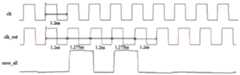
图4所示为自适应时钟拉伸原理时序图。时钟拉伸的操作就是根据监测关键路径时序信息的不同,选择所需的目标相位时钟,使得整个系统功能正确,满足时序要求。本发明以图4为例具体说明时钟拉伸原理,即每个周期内对上一周期的系统输入时钟信号进行合理的拉伸操作。初始输入的系统时钟为clk,第一个周期内,系统关键路径末端的TD监测得到时序预警信号error_all反馈给监测单元组电路(TD+锁存器)生成monitor_wide信号传递给控制模块产生时钟选择控制信号ctrl[N:1],其中,ctrl[1]=1,ctrl[N:2]=0,则系统选择相位时钟Φ1为目标时钟进行拉伸,即下一周期的上升沿为相位时钟Φ1的上升沿位置;第二个周期内,同样地,产生的时钟选择控制信号中ctrl[4]=1,其余位全为0,则系统选择相位时钟Φ4为目标时钟进行拉伸,即下一周期的上升沿为相位时钟Φ4的上升沿位置。整个系统按照此规则完成时钟拉伸,时钟压缩的原理类似。Figure 4 shows the timing diagram of the principle of adaptive clock stretching. The operation of clock stretching is to select the required target phase clock according to the difference in monitoring critical path timing information, so that the entire system functions correctly and meets the timing requirements. The present invention takes FIG. 4 as an example to specifically illustrate the clock stretching principle, that is, a reasonable stretching operation is performed on the system input clock signal of the previous cycle in each cycle. The initial input system clock is clk. In the first cycle, the TD monitoring at the end of the critical path of the system obtains the timing early warning signal error_all and feeds it back to the monitoring unit group circuit (TD+ latch) to generate the monitor_wide signal and transmit it to the control module to generate the clock selection control signal ctrl[N:1], where ctrl[1]=1, ctrl[N:2]=0, then the system selects the phase clock Φ1 as the target clock for stretching, that is, the rising edge of the next cycle is the phase clock Φ1 Rising edge position; in the second cycle, in the same way, in the generated clock selection control signal, ctrl[4]=1, and the rest of the bits are all 0, then the system selects the phase clock Φ4 as the target clock to stretch, that is, the next cycle The rising edge of is the position of the rising edge of the phase clock Φ4. The entire system completes clock stretching according to this rule, and the principle of clock compression is similar.
在本发明的支持宽频率范围的双向自适应时钟电路的一个具体实施案例中,将本发明提出的电路搭载在8比特AES密码电路平台上进行自适应时钟拉伸或压缩功能验证。采用SMIC提供的28nm工艺库,利用Synopsys公司提供的VCS和HSIM等软件仿真平台,在不同PVT环境下对该电路进行功能仿真测试。基于上述技术方案设计各个模块的电路结构,利用Verilog HDL语言对电路进行建模,对其电路功能进行仿真验证。设定电路相位时钟生成模块两条延迟线中延时单元数目N为40(每条延迟线包含20个延时单元)。分别将电路置于不同时钟频率条件及不同PVT条件下进行仿真,得到仿真结果如图5、图6、图7所示。In a specific implementation case of the bidirectional adaptive clock circuit supporting a wide frequency range of the present invention, the circuit proposed by the present invention is mounted on an 8-bit AES cryptographic circuit platform to perform adaptive clock stretching or compression function verification. Using the 28nm process library provided by SMIC, and using the software simulation platforms such as VCS and HSIM provided by Synopsys, the function simulation test of the circuit is carried out in different PVT environments. Based on the above technical solutions, the circuit structure of each module is designed, the circuit is modeled by Verilog HDL language, and its circuit function is simulated and verified. The number N of delay units in the two delay lines of the circuit phase clock generation module is set to be 40 (each delay line contains 20 delay units). The circuit is simulated under different clock frequency conditions and different PVT conditions, and the simulation results are shown in Figure 5, Figure 6, and Figure 7.
图5所示的是整体系统功能验证的波形图。设置系统当前所处PVT环境为TT工艺角,1.05V以及25℃,系统时钟频率为710MHz,即时钟周期约为1.4ns。此时系统时序比较宽松,error_all时序预警信号拉低,因此,系统开启自适应时钟压缩功能,压缩了时序余量。同时,8比特AES密码电路平台产生的flag_out功能信号在完成一次加密后拉高,表明系统功能在结合自适应时钟压缩功能的情况下正确。Figure 5 shows the waveform diagram of the overall system functional verification. Set the PVT environment where the system is currently located as the TT process angle, 1.05V and 25°C, and the system clock frequency is 710MHz, that is, the clock cycle is about 1.4ns. At this time, the system timing is relatively loose, and the error_all timing warning signal is pulled low. Therefore, the system enables the adaptive clock compression function to compress the timing margin. At the same time, the flag_out function signal generated by the 8-bit AES cryptographic circuit platform is pulled high after completing one encryption, indicating that the system function is correct when combined with the adaptive clock compression function.
图6所示的是常规电压区下系统实现自适应时钟拉伸的波形图。设置系统当前所处PVT环境为TT工艺角,1.05V以及25℃,系统时钟频率为830MHz,即周期约为1.2ns。当系统时序比较紧张时,产生error_all时序预警信号。该信号立即反馈给自适应时钟拉伸电路,并在当周期拉伸时钟至时钟周期为1.275ns,有效缓解了常规电压下系统的时序紧张问题。Figure 6 shows the waveform diagram of the system achieving adaptive clock stretching in the conventional voltage region. Set the PVT environment where the system is currently located as the TT process angle, 1.05V and 25°C, and the system clock frequency is 830MHz, that is, the period is about 1.2ns. When the system timing is relatively tight, the error_all timing early warning signal is generated. The signal is immediately fed back to the adaptive clock stretching circuit, and the clock is stretched to a clock period of 1.275ns in the current period, which effectively relieves the system's timing tension problem under conventional voltage.
图7所示的是低电压区下系统实现自适应时钟拉伸的波形图。设置系统当前所处PVT环境为TT工艺角,0.6V以及25℃,系统时钟频率为100MHz,即周期为10ns。当系统时序比较紧张时,产生error_all时序预警信号。该信号立即反馈给自适应时钟拉伸电路,并在当周期拉伸时钟至时钟周期为10.42ns,有效缓解了低电压下系统的时序紧张问题。Figure 7 shows the waveform diagram of the system implementing adaptive clock stretching in the low voltage region. Set the PVT environment where the system is currently located as TT process angle, 0.6V and 25°C, and the system clock frequency is 100MHz, that is, the period is 10ns. When the system timing is relatively tight, the error_all timing early warning signal is generated. The signal is immediately fed back to the adaptive clock stretching circuit, and the clock is stretched to a clock period of 10.42ns in the current period, which effectively alleviates the problem of timing tension of the system under low voltage.
可见,本发明尤其适合用于基于在线时序监测的自适应电压频率调节电路,当电路运行出现时序违约时,则产生控制信号使时钟拉伸,增加电路时序余量,从而避免电路工作出错;当时序余量比较充足时,则使时钟压缩,尽可能降低时序余量,从而提升电路性能,降低功耗。It can be seen that the present invention is especially suitable for an adaptive voltage and frequency adjustment circuit based on on-line timing monitoring. When a timing violation occurs in the operation of the circuit, a control signal is generated to stretch the clock and increase the timing margin of the circuit, thereby avoiding circuit operation errors; When the sequence margin is sufficient, the clock is compressed to reduce the sequence margin as much as possible, thereby improving circuit performance and reducing power consumption.
以上结果显示了本发明能够在当前周期内迅速实现时钟拉伸或压缩的功能,整体系统功能正确,使用的自适应时钟电路结构简单,精度较好,误差较小。The above results show that the present invention can quickly realize the clock stretching or compressing function in the current cycle, the overall system function is correct, and the adaptive clock circuit used has a simple structure, good precision and small error.
Claims (7)
Translated fromChinesePriority Applications (3)
| Application Number | Priority Date | Filing Date | Title |
|---|---|---|---|
| CN201910514122.5ACN110336545B (en) | 2019-06-14 | 2019-06-14 | A Bidirectional Adaptive Clock Circuit Supporting Wide Frequency Range |
| PCT/CN2019/095202WO2020248318A1 (en) | 2019-06-14 | 2019-07-09 | Bidirectional adaptive clock circuit supporting wide frequency range |
| US16/957,724US11139805B1 (en) | 2019-06-14 | 2019-07-09 | Bi-directional adaptive clocking circuit supporting a wide frequency range |
Applications Claiming Priority (1)
| Application Number | Priority Date | Filing Date | Title |
|---|---|---|---|
| CN201910514122.5ACN110336545B (en) | 2019-06-14 | 2019-06-14 | A Bidirectional Adaptive Clock Circuit Supporting Wide Frequency Range |
Publications (2)
| Publication Number | Publication Date |
|---|---|
| CN110336545A CN110336545A (en) | 2019-10-15 |
| CN110336545Btrue CN110336545B (en) | 2020-08-04 |
Family
ID=68142062
Family Applications (1)
| Application Number | Title | Priority Date | Filing Date |
|---|---|---|---|
| CN201910514122.5AActiveCN110336545B (en) | 2019-06-14 | 2019-06-14 | A Bidirectional Adaptive Clock Circuit Supporting Wide Frequency Range |
Country Status (3)
| Country | Link |
|---|---|
| US (1) | US11139805B1 (en) |
| CN (1) | CN110336545B (en) |
| WO (1) | WO2020248318A1 (en) |
Families Citing this family (133)
| Publication number | Priority date | Publication date | Assignee | Title |
|---|---|---|---|---|
| US20070084897A1 (en) | 2003-05-20 | 2007-04-19 | Shelton Frederick E Iv | Articulating surgical stapling instrument incorporating a two-piece e-beam firing mechanism |
| US9060770B2 (en) | 2003-05-20 | 2015-06-23 | Ethicon Endo-Surgery, Inc. | Robotically-driven surgical instrument with E-beam driver |
| US11890012B2 (en) | 2004-07-28 | 2024-02-06 | Cilag Gmbh International | Staple cartridge comprising cartridge body and attached support |
| US11998198B2 (en) | 2004-07-28 | 2024-06-04 | Cilag Gmbh International | Surgical stapling instrument incorporating a two-piece E-beam firing mechanism |
| US9072535B2 (en) | 2011-05-27 | 2015-07-07 | Ethicon Endo-Surgery, Inc. | Surgical stapling instruments with rotatable staple deployment arrangements |
| US10159482B2 (en) | 2005-08-31 | 2018-12-25 | Ethicon Llc | Fastener cartridge assembly comprising a fixed anvil and different staple heights |
| US11246590B2 (en) | 2005-08-31 | 2022-02-15 | Cilag Gmbh International | Staple cartridge including staple drivers having different unfired heights |
| US7669746B2 (en) | 2005-08-31 | 2010-03-02 | Ethicon Endo-Surgery, Inc. | Staple cartridges for forming staples having differing formed staple heights |
| US8186555B2 (en) | 2006-01-31 | 2012-05-29 | Ethicon Endo-Surgery, Inc. | Motor-driven surgical cutting and fastening instrument with mechanical closure system |
| US7845537B2 (en) | 2006-01-31 | 2010-12-07 | Ethicon Endo-Surgery, Inc. | Surgical instrument having recording capabilities |
| US20120292367A1 (en) | 2006-01-31 | 2012-11-22 | Ethicon Endo-Surgery, Inc. | Robotically-controlled end effector |
| US8708213B2 (en) | 2006-01-31 | 2014-04-29 | Ethicon Endo-Surgery, Inc. | Surgical instrument having a feedback system |
| US11793518B2 (en) | 2006-01-31 | 2023-10-24 | Cilag Gmbh International | Powered surgical instruments with firing system lockout arrangements |
| US8992422B2 (en) | 2006-03-23 | 2015-03-31 | Ethicon Endo-Surgery, Inc. | Robotically-controlled endoscopic accessory channel |
| US11980366B2 (en) | 2006-10-03 | 2024-05-14 | Cilag Gmbh International | Surgical instrument |
| US8684253B2 (en) | 2007-01-10 | 2014-04-01 | Ethicon Endo-Surgery, Inc. | Surgical instrument with wireless communication between a control unit of a robotic system and remote sensor |
| US8632535B2 (en) | 2007-01-10 | 2014-01-21 | Ethicon Endo-Surgery, Inc. | Interlock and surgical instrument including same |
| US20080169333A1 (en) | 2007-01-11 | 2008-07-17 | Shelton Frederick E | Surgical stapler end effector with tapered distal end |
| US8931682B2 (en) | 2007-06-04 | 2015-01-13 | Ethicon Endo-Surgery, Inc. | Robotically-controlled shaft based rotary drive systems for surgical instruments |
| US11564682B2 (en) | 2007-06-04 | 2023-01-31 | Cilag Gmbh International | Surgical stapler device |
| US11849941B2 (en) | 2007-06-29 | 2023-12-26 | Cilag Gmbh International | Staple cartridge having staple cavities extending at a transverse angle relative to a longitudinal cartridge axis |
| JP5410110B2 (en) | 2008-02-14 | 2014-02-05 | エシコン・エンド−サージェリィ・インコーポレイテッド | Surgical cutting / fixing instrument with RF electrode |
| US8573465B2 (en) | 2008-02-14 | 2013-11-05 | Ethicon Endo-Surgery, Inc. | Robotically-controlled surgical end effector system with rotary actuated closure systems |
| US8636736B2 (en) | 2008-02-14 | 2014-01-28 | Ethicon Endo-Surgery, Inc. | Motorized surgical cutting and fastening instrument |
| US11986183B2 (en) | 2008-02-14 | 2024-05-21 | Cilag Gmbh International | Surgical cutting and fastening instrument comprising a plurality of sensors to measure an electrical parameter |
| US9585657B2 (en) | 2008-02-15 | 2017-03-07 | Ethicon Endo-Surgery, Llc | Actuator for releasing a layer of material from a surgical end effector |
| US8210411B2 (en) | 2008-09-23 | 2012-07-03 | Ethicon Endo-Surgery, Inc. | Motor-driven surgical cutting instrument |
| US9005230B2 (en) | 2008-09-23 | 2015-04-14 | Ethicon Endo-Surgery, Inc. | Motorized surgical instrument |
| US9386983B2 (en) | 2008-09-23 | 2016-07-12 | Ethicon Endo-Surgery, Llc | Robotically-controlled motorized surgical instrument |
| US8608045B2 (en) | 2008-10-10 | 2013-12-17 | Ethicon Endo-Sugery, Inc. | Powered surgical cutting and stapling apparatus with manually retractable firing system |
| US12213666B2 (en) | 2010-09-30 | 2025-02-04 | Cilag Gmbh International | Tissue thickness compensator comprising layers |
| US9629814B2 (en) | 2010-09-30 | 2017-04-25 | Ethicon Endo-Surgery, Llc | Tissue thickness compensator configured to redistribute compressive forces |
| US11925354B2 (en) | 2010-09-30 | 2024-03-12 | Cilag Gmbh International | Staple cartridge comprising staples positioned within a compressible portion thereof |
| US11812965B2 (en) | 2010-09-30 | 2023-11-14 | Cilag Gmbh International | Layer of material for a surgical end effector |
| US10945731B2 (en) | 2010-09-30 | 2021-03-16 | Ethicon Llc | Tissue thickness compensator comprising controlled release and expansion |
| US9788834B2 (en) | 2010-09-30 | 2017-10-17 | Ethicon Llc | Layer comprising deployable attachment members |
| US9386988B2 (en) | 2010-09-30 | 2016-07-12 | Ethicon End-Surgery, LLC | Retainer assembly including a tissue thickness compensator |
| AU2012250197B2 (en) | 2011-04-29 | 2017-08-10 | Ethicon Endo-Surgery, Inc. | Staple cartridge comprising staples positioned within a compressible portion thereof |
| US11207064B2 (en) | 2011-05-27 | 2021-12-28 | Cilag Gmbh International | Automated end effector component reloading system for use with a robotic system |
| MX358135B (en) | 2012-03-28 | 2018-08-06 | Ethicon Endo Surgery Inc | Tissue thickness compensator comprising a plurality of layers. |
| BR112014024098B1 (en) | 2012-03-28 | 2021-05-25 | Ethicon Endo-Surgery, Inc. | staple cartridge |
| US20140001231A1 (en) | 2012-06-28 | 2014-01-02 | Ethicon Endo-Surgery, Inc. | Firing system lockout arrangements for surgical instruments |
| US9289256B2 (en) | 2012-06-28 | 2016-03-22 | Ethicon Endo-Surgery, Llc | Surgical end effectors having angled tissue-contacting surfaces |
| US12383267B2 (en) | 2012-06-28 | 2025-08-12 | Cilag Gmbh International | Robotically powered surgical device with manually-actuatable reversing system |
| RU2672520C2 (en) | 2013-03-01 | 2018-11-15 | Этикон Эндо-Серджери, Инк. | Hingedly turnable surgical instruments with conducting ways for signal transfer |
| US9629629B2 (en) | 2013-03-14 | 2017-04-25 | Ethicon Endo-Surgey, LLC | Control systems for surgical instruments |
| BR112015026109B1 (en) | 2013-04-16 | 2022-02-22 | Ethicon Endo-Surgery, Inc | surgical instrument |
| US9775609B2 (en) | 2013-08-23 | 2017-10-03 | Ethicon Llc | Tamper proof circuit for surgical instrument battery pack |
| US10013049B2 (en) | 2014-03-26 | 2018-07-03 | Ethicon Llc | Power management through sleep options of segmented circuit and wake up control |
| US12232723B2 (en) | 2014-03-26 | 2025-02-25 | Cilag Gmbh International | Systems and methods for controlling a segmented circuit |
| BR112016023825B1 (en) | 2014-04-16 | 2022-08-02 | Ethicon Endo-Surgery, Llc | STAPLE CARTRIDGE FOR USE WITH A SURGICAL STAPLER AND STAPLE CARTRIDGE FOR USE WITH A SURGICAL INSTRUMENT |
| CN106456176B (en) | 2014-04-16 | 2019-06-28 | 伊西康内外科有限责任公司 | Fastener Cartridge Including Extensions With Different Configurations |
| US10327764B2 (en) | 2014-09-26 | 2019-06-25 | Ethicon Llc | Method for creating a flexible staple line |
| CN106456159B (en) | 2014-04-16 | 2019-03-08 | 伊西康内外科有限责任公司 | Fastener Cartridge Assembly and Nail Retainer Cover Arrangement |
| US20150297225A1 (en) | 2014-04-16 | 2015-10-22 | Ethicon Endo-Surgery, Inc. | Fastener cartridges including extensions having different configurations |
| US11311294B2 (en) | 2014-09-05 | 2022-04-26 | Cilag Gmbh International | Powered medical device including measurement of closure state of jaws |
| BR112017004361B1 (en) | 2014-09-05 | 2023-04-11 | Ethicon Llc | ELECTRONIC SYSTEM FOR A SURGICAL INSTRUMENT |
| US10105142B2 (en) | 2014-09-18 | 2018-10-23 | Ethicon Llc | Surgical stapler with plurality of cutting elements |
| US9924944B2 (en) | 2014-10-16 | 2018-03-27 | Ethicon Llc | Staple cartridge comprising an adjunct material |
| US9987000B2 (en) | 2014-12-18 | 2018-06-05 | Ethicon Llc | Surgical instrument assembly comprising a flexible articulation system |
| US11154301B2 (en) | 2015-02-27 | 2021-10-26 | Cilag Gmbh International | Modular stapling assembly |
| US10441279B2 (en) | 2015-03-06 | 2019-10-15 | Ethicon Llc | Multiple level thresholds to modify operation of powered surgical instruments |
| US10433844B2 (en) | 2015-03-31 | 2019-10-08 | Ethicon Llc | Surgical instrument with selectively disengageable threaded drive systems |
| US10105139B2 (en) | 2015-09-23 | 2018-10-23 | Ethicon Llc | Surgical stapler having downstream current-based motor control |
| US10299878B2 (en) | 2015-09-25 | 2019-05-28 | Ethicon Llc | Implantable adjunct systems for determining adjunct skew |
| US10478188B2 (en) | 2015-09-30 | 2019-11-19 | Ethicon Llc | Implantable layer comprising a constricted configuration |
| US11890015B2 (en) | 2015-09-30 | 2024-02-06 | Cilag Gmbh International | Compressible adjunct with crossing spacer fibers |
| US10265068B2 (en) | 2015-12-30 | 2019-04-23 | Ethicon Llc | Surgical instruments with separable motors and motor control circuits |
| US10292704B2 (en) | 2015-12-30 | 2019-05-21 | Ethicon Llc | Mechanisms for compensating for battery pack failure in powered surgical instruments |
| US11213293B2 (en) | 2016-02-09 | 2022-01-04 | Cilag Gmbh International | Articulatable surgical instruments with single articulation link arrangements |
| US10448948B2 (en) | 2016-02-12 | 2019-10-22 | Ethicon Llc | Mechanisms for compensating for drivetrain failure in powered surgical instruments |
| US10828028B2 (en) | 2016-04-15 | 2020-11-10 | Ethicon Llc | Surgical instrument with multiple program responses during a firing motion |
| US10357247B2 (en) | 2016-04-15 | 2019-07-23 | Ethicon Llc | Surgical instrument with multiple program responses during a firing motion |
| US20170296173A1 (en) | 2016-04-18 | 2017-10-19 | Ethicon Endo-Surgery, Llc | Method for operating a surgical instrument |
| US10500000B2 (en) | 2016-08-16 | 2019-12-10 | Ethicon Llc | Surgical tool with manual control of end effector jaws |
| US20180168625A1 (en) | 2016-12-21 | 2018-06-21 | Ethicon Endo-Surgery, Llc | Surgical stapling instruments with smart staple cartridges |
| US10973516B2 (en) | 2016-12-21 | 2021-04-13 | Ethicon Llc | Surgical end effectors and adaptable firing members therefor |
| JP7010957B2 (en) | 2016-12-21 | 2022-01-26 | エシコン エルエルシー | Shaft assembly with lockout |
| US10813638B2 (en) | 2016-12-21 | 2020-10-27 | Ethicon Llc | Surgical end effectors with expandable tissue stop arrangements |
| JP7010956B2 (en) | 2016-12-21 | 2022-01-26 | エシコン エルエルシー | How to staple tissue |
| US10779820B2 (en) | 2017-06-20 | 2020-09-22 | Ethicon Llc | Systems and methods for controlling motor speed according to user input for a surgical instrument |
| US10307170B2 (en) | 2017-06-20 | 2019-06-04 | Ethicon Llc | Method for closed loop control of motor velocity of a surgical stapling and cutting instrument |
| EP3420947B1 (en) | 2017-06-28 | 2022-05-25 | Cilag GmbH International | Surgical instrument comprising selectively actuatable rotatable couplers |
| USD906355S1 (en) | 2017-06-28 | 2020-12-29 | Ethicon Llc | Display screen or portion thereof with a graphical user interface for a surgical instrument |
| US10932772B2 (en) | 2017-06-29 | 2021-03-02 | Ethicon Llc | Methods for closed loop velocity control for robotic surgical instrument |
| US11974742B2 (en) | 2017-08-03 | 2024-05-07 | Cilag Gmbh International | Surgical system comprising an articulation bailout |
| US11134944B2 (en) | 2017-10-30 | 2021-10-05 | Cilag Gmbh International | Surgical stapler knife motion controls |
| US10842490B2 (en) | 2017-10-31 | 2020-11-24 | Ethicon Llc | Cartridge body design with force reduction based on firing completion |
| US10779826B2 (en) | 2017-12-15 | 2020-09-22 | Ethicon Llc | Methods of operating surgical end effectors |
| US10835330B2 (en) | 2017-12-19 | 2020-11-17 | Ethicon Llc | Method for determining the position of a rotatable jaw of a surgical instrument attachment assembly |
| US12336705B2 (en) | 2017-12-21 | 2025-06-24 | Cilag Gmbh International | Continuous use self-propelled stapling instrument |
| US11179151B2 (en) | 2017-12-21 | 2021-11-23 | Cilag Gmbh International | Surgical instrument comprising a display |
| US11291440B2 (en) | 2018-08-20 | 2022-04-05 | Cilag Gmbh International | Method for operating a powered articulatable surgical instrument |
| US11207065B2 (en) | 2018-08-20 | 2021-12-28 | Cilag Gmbh International | Method for fabricating surgical stapler anvils |
| US20200054321A1 (en) | 2018-08-20 | 2020-02-20 | Ethicon Llc | Surgical instruments with progressive jaw closure arrangements |
| US20200345359A1 (en) | 2019-04-30 | 2020-11-05 | Ethicon Llc | Tissue stop for a surgical instrument |
| US11903581B2 (en) | 2019-04-30 | 2024-02-20 | Cilag Gmbh International | Methods for stapling tissue using a surgical instrument |
| US11241235B2 (en) | 2019-06-28 | 2022-02-08 | Cilag Gmbh International | Method of using multiple RFID chips with a surgical assembly |
| US12035913B2 (en) | 2019-12-19 | 2024-07-16 | Cilag Gmbh International | Staple cartridge comprising a deployable knife |
| USD1013170S1 (en) | 2020-10-29 | 2024-01-30 | Cilag Gmbh International | Surgical instrument assembly |
| US11779330B2 (en) | 2020-10-29 | 2023-10-10 | Cilag Gmbh International | Surgical instrument comprising a jaw alignment system |
| US11931025B2 (en) | 2020-10-29 | 2024-03-19 | Cilag Gmbh International | Surgical instrument comprising a releasable closure drive lock |
| US11944296B2 (en) | 2020-12-02 | 2024-04-02 | Cilag Gmbh International | Powered surgical instruments with external connectors |
| US11849943B2 (en) | 2020-12-02 | 2023-12-26 | Cilag Gmbh International | Surgical instrument with cartridge release mechanisms |
| US11737751B2 (en) | 2020-12-02 | 2023-08-29 | Cilag Gmbh International | Devices and methods of managing energy dissipated within sterile barriers of surgical instrument housings |
| CN112763890B (en)* | 2020-12-15 | 2022-09-16 | 成都海光微电子技术有限公司 | Implementation method of test circuit for adaptive voltage and frequency regulation of chip |
| US11744583B2 (en) | 2021-02-26 | 2023-09-05 | Cilag Gmbh International | Distal communication array to tune frequency of RF systems |
| US11812964B2 (en) | 2021-02-26 | 2023-11-14 | Cilag Gmbh International | Staple cartridge comprising a power management circuit |
| US11925349B2 (en)* | 2021-02-26 | 2024-03-12 | Cilag Gmbh International | Adjustment to transfer parameters to improve available power |
| US11749877B2 (en) | 2021-02-26 | 2023-09-05 | Cilag Gmbh International | Stapling instrument comprising a signal antenna |
| US12108951B2 (en) | 2021-02-26 | 2024-10-08 | Cilag Gmbh International | Staple cartridge comprising a sensing array and a temperature control system |
| US11751869B2 (en) | 2021-02-26 | 2023-09-12 | Cilag Gmbh International | Monitoring of multiple sensors over time to detect moving characteristics of tissue |
| US11826012B2 (en) | 2021-03-22 | 2023-11-28 | Cilag Gmbh International | Stapling instrument comprising a pulsed motor-driven firing rack |
| US11737749B2 (en) | 2021-03-22 | 2023-08-29 | Cilag Gmbh International | Surgical stapling instrument comprising a retraction system |
| US11806011B2 (en) | 2021-03-22 | 2023-11-07 | Cilag Gmbh International | Stapling instrument comprising tissue compression systems |
| US11826042B2 (en) | 2021-03-22 | 2023-11-28 | Cilag Gmbh International | Surgical instrument comprising a firing drive including a selectable leverage mechanism |
| US11723658B2 (en) | 2021-03-22 | 2023-08-15 | Cilag Gmbh International | Staple cartridge comprising a firing lockout |
| US11896219B2 (en) | 2021-03-24 | 2024-02-13 | Cilag Gmbh International | Mating features between drivers and underside of a cartridge deck |
| US11849945B2 (en) | 2021-03-24 | 2023-12-26 | Cilag Gmbh International | Rotary-driven surgical stapling assembly comprising eccentrically driven firing member |
| US11744603B2 (en) | 2021-03-24 | 2023-09-05 | Cilag Gmbh International | Multi-axis pivot joints for surgical instruments and methods for manufacturing same |
| US11826047B2 (en) | 2021-05-28 | 2023-11-28 | Cilag Gmbh International | Stapling instrument comprising jaw mounts |
| CN113707209B (en)* | 2021-08-31 | 2025-09-30 | 上海华力集成电路制造有限公司 | Dynamically adjustable clock path circuit |
| US11980363B2 (en) | 2021-10-18 | 2024-05-14 | Cilag Gmbh International | Row-to-row staple array variations |
| US12089841B2 (en) | 2021-10-28 | 2024-09-17 | Cilag CmbH International | Staple cartridge identification systems |
| US12432790B2 (en) | 2021-10-28 | 2025-09-30 | Cilag Gmbh International | Method and device for transmitting UART communications over a security short range wireless communication |
| US11937816B2 (en) | 2021-10-28 | 2024-03-26 | Cilag Gmbh International | Electrical lead arrangements for surgical instruments |
| CN114253346B (en)* | 2021-12-09 | 2024-09-24 | 杭州长川科技股份有限公司 | Timing signal generator and calibration system and method thereof |
| CN114546801B (en)* | 2022-02-14 | 2025-07-15 | 上海交通大学 | A timing margin monitoring and compression method and circuit for deep pipeline circuits |
| CN114968865B (en)* | 2022-07-22 | 2022-09-27 | 中科声龙科技发展(北京)有限公司 | Bus transmission structure and method and chip |
| CN115576386B (en)* | 2022-11-14 | 2023-06-27 | 南京芯驰半导体科技有限公司 | Signal delay adjustment chip, method, equipment and storage medium |
| US12158771B2 (en) | 2023-03-31 | 2024-12-03 | International Business Machines Corporation | Clock gating circuit for avoiding out-of-spec clock operations in self-timed circuits |
| CN117272879B (en)* | 2023-09-19 | 2024-07-05 | 武汉泰朴半导体有限公司 | All-digital clock generation circuit and all-digital clock generation method |
| CN119602758A (en)* | 2025-02-13 | 2025-03-11 | 中茵微电子(南京)有限公司 | A low-latency cross-asynchronous method and circuit based on chiplet interconnection direction |
Citations (5)
| Publication number | Priority date | Publication date | Assignee | Title |
|---|---|---|---|---|
| US5963070A (en)* | 1997-06-02 | 1999-10-05 | Advanced Micro Devices, Inc. | Stretch cycle generator |
| CN106026994A (en)* | 2016-05-16 | 2016-10-12 | 东南大学 | Wide voltage clock stretching circuit based on PVTM |
| CN106209031A (en)* | 2016-07-18 | 2016-12-07 | 珠海格力电器股份有限公司 | Clock circuit, clock signal generating method, and control chip including the clock circuit |
| CN106294284A (en)* | 2016-08-26 | 2017-01-04 | 河海大学 | Rainfall KPT Scatter computing accelerated method based on frequency angle two-dimensional mixing interpolation |
| CN207425319U (en)* | 2017-08-31 | 2018-05-29 | 深圳市明微电子股份有限公司 | A kind of decoding circuit of self-adapting data frequency |
Family Cites Families (4)
| Publication number | Priority date | Publication date | Assignee | Title |
|---|---|---|---|---|
| CN103500243B (en)* | 2013-09-04 | 2016-08-17 | 深圳市国微电子有限公司 | A kind of clock circuit method for designing of self adaptation PVT change |
| CN103997338B (en)* | 2014-05-29 | 2018-07-31 | 华为技术有限公司 | Delayer and delay locked loop circuit |
| CN105978539B (en)* | 2016-05-16 | 2019-01-04 | 东南大学 | A kind of quick clock that structure is simplified stretching circuit |
| US10148258B2 (en)* | 2016-09-28 | 2018-12-04 | Mellanox Technologies, Ltd. | Power supply voltage monitoring and high-resolution adaptive clock stretching circuit |
- 2019
- 2019-06-14CNCN201910514122.5Apatent/CN110336545B/enactiveActive
- 2019-07-09WOPCT/CN2019/095202patent/WO2020248318A1/ennot_activeCeased
- 2019-07-09USUS16/957,724patent/US11139805B1/enactiveActive
Patent Citations (5)
| Publication number | Priority date | Publication date | Assignee | Title |
|---|---|---|---|---|
| US5963070A (en)* | 1997-06-02 | 1999-10-05 | Advanced Micro Devices, Inc. | Stretch cycle generator |
| CN106026994A (en)* | 2016-05-16 | 2016-10-12 | 东南大学 | Wide voltage clock stretching circuit based on PVTM |
| CN106209031A (en)* | 2016-07-18 | 2016-12-07 | 珠海格力电器股份有限公司 | Clock circuit, clock signal generating method, and control chip including the clock circuit |
| CN106294284A (en)* | 2016-08-26 | 2017-01-04 | 河海大学 | Rainfall KPT Scatter computing accelerated method based on frequency angle two-dimensional mixing interpolation |
| CN207425319U (en)* | 2017-08-31 | 2018-05-29 | 深圳市明微电子股份有限公司 | A kind of decoding circuit of self-adapting data frequency |
Also Published As
| Publication number | Publication date |
|---|---|
| CN110336545A (en) | 2019-10-15 |
| WO2020248318A1 (en) | 2020-12-17 |
| US11139805B1 (en) | 2021-10-05 |
| US20210313975A1 (en) | 2021-10-07 |
Similar Documents
| Publication | Publication Date | Title |
|---|---|---|
| CN110336545B (en) | A Bidirectional Adaptive Clock Circuit Supporting Wide Frequency Range | |
| CN105159374B (en) | On-line monitoring unit and monitoring window self-adaption regulation system towards super wide voltage | |
| CN106026994A (en) | Wide voltage clock stretching circuit based on PVTM | |
| CN103546125B (en) | A kind of multiselect one burr-free clock switching circuit | |
| US6750692B2 (en) | Circuit and method for generating internal clock signal | |
| CN102077505B (en) | Clock transfer circuit and tester using the same | |
| KR20210128031A (en) | Apparatuses and methods for detecting a loop count in a delay-locked loop | |
| CN110649922A (en) | Digital clock frequency multiplier | |
| CN105978539A (en) | Quick clock stretching circuit of simplified structure | |
| CN101645301B (en) | Temperature self-adaptive adjustment method for read data sampling and device thereof | |
| JP3851113B2 (en) | Clock generator with deskew circuit | |
| CN114167943A (en) | Clock skew adjustable chip clock architecture of programmable logic chip | |
| CN111710353A (en) | Double data rate circuit and data generation method implementing precise duty cycle control | |
| US6550013B1 (en) | Memory clock generator and method therefor | |
| US8395946B2 (en) | Data access apparatus and associated method for accessing data using internally generated clocks | |
| Amini et al. | Globally asynchronous locally synchronous wrapper circuit based on clock gating | |
| KR20050099714A (en) | High dendsity low power glitchless clock selection circuit and digital processing system including the same | |
| US9698796B2 (en) | Dynamic clock synchronization | |
| WO2022110235A1 (en) | Chip and clock detection method | |
| CN117639749A (en) | Low-power-consumption multi-clock domain clock reset system and chip | |
| US20230396253A1 (en) | Anti-aging clock source multiplexing | |
| US6982573B2 (en) | Switchable clock source | |
| JPH0865173A (en) | Parallel to serial conversion circuit | |
| CN113504809A (en) | Dynamic switching method, device and system of multi-channel clock | |
| CN101800543A (en) | High-speed dual-mode 7/8 frequency divider based on phase switch |
Legal Events
| Date | Code | Title | Description |
|---|---|---|---|
| PB01 | Publication | ||
| PB01 | Publication | ||
| SE01 | Entry into force of request for substantive examination | ||
| SE01 | Entry into force of request for substantive examination | ||
| GR01 | Patent grant | ||
| GR01 | Patent grant | ||
| EE01 | Entry into force of recordation of patent licensing contract | ||
| EE01 | Entry into force of recordation of patent licensing contract | Application publication date:20191015 Assignee:HUAWEI TECHNOLOGIES Co.,Ltd. Assignor:SOUTHEAST University Contract record no.:X2022980004192 Denomination of invention:A bidirectional adaptive clock circuit supporting wide frequency range Granted publication date:20200804 License type:Common License Record date:20220414 |