CN110323575B - Dual-polarized strongly coupled ultra-wideband phased array antenna loaded with electromagnetic metamaterials - Google Patents
Dual-polarized strongly coupled ultra-wideband phased array antenna loaded with electromagnetic metamaterialsDownload PDFInfo
- Publication number
- CN110323575B CN110323575BCN201910386194.6ACN201910386194ACN110323575BCN 110323575 BCN110323575 BCN 110323575BCN 201910386194 ACN201910386194 ACN 201910386194ACN 110323575 BCN110323575 BCN 110323575B
- Authority
- CN
- China
- Prior art keywords
- antenna
- dielectric substrate
- coupling
- strong
- folded dipole
- Prior art date
- Legal status (The legal status is an assumption and is not a legal conclusion. Google has not performed a legal analysis and makes no representation as to the accuracy of the status listed.)
- Active
Links
- 239000000758substrateSubstances0.000claimsabstractdescription49
- 238000010168coupling processMethods0.000claimsabstractdescription36
- 238000005859coupling reactionMethods0.000claimsabstractdescription36
- 230000008878couplingEffects0.000claimsabstractdescription25
- 230000010287polarizationEffects0.000claimsdescription27
- 230000003071parasitic effectEffects0.000claimsdescription13
- 230000008859changeEffects0.000claimsdescription2
- 230000003014reinforcing effectEffects0.000claims1
- 238000005388cross polarizationMethods0.000abstractdescription15
- 238000013461designMethods0.000abstractdescription3
- 230000000694effectsEffects0.000abstractdescription3
- 230000005855radiationEffects0.000abstractdescription3
- 238000010586diagramMethods0.000description4
- 238000005516engineering processMethods0.000description4
- 238000012545processingMethods0.000description4
- 230000009466transformationEffects0.000description4
- 230000001808coupling effectEffects0.000description3
- 238000000034methodMethods0.000description3
- 230000000737periodic effectEffects0.000description3
- 238000003491arrayMethods0.000description2
- 238000004891communicationMethods0.000description2
- 238000011161developmentMethods0.000description2
- 230000002708enhancing effectEffects0.000description2
- 238000005452bendingMethods0.000description1
- 230000009286beneficial effectEffects0.000description1
- 230000015572biosynthetic processEffects0.000description1
- 230000007812deficiencyEffects0.000description1
- 238000001514detection methodMethods0.000description1
- 238000009826distributionMethods0.000description1
- 230000009977dual effectEffects0.000description1
- 238000009434installationMethods0.000description1
- 230000010354integrationEffects0.000description1
- 238000002955isolationMethods0.000description1
- 238000012423maintenanceMethods0.000description1
- 238000004519manufacturing processMethods0.000description1
- 239000002184metalSubstances0.000description1
- 230000002787reinforcementEffects0.000description1
- 238000011160researchMethods0.000description1
- 238000005728strengtheningMethods0.000description1
- 238000003786synthesis reactionMethods0.000description1
- 238000012876topographyMethods0.000description1
- 238000003466weldingMethods0.000description1
Images


Classifications
- H—ELECTRICITY
- H01—ELECTRIC ELEMENTS
- H01Q—ANTENNAS, i.e. RADIO AERIALS
- H01Q1/00—Details of, or arrangements associated with, antennas
- H01Q1/36—Structural form of radiating elements, e.g. cone, spiral, umbrella; Particular materials used therewith
- H01Q1/38—Structural form of radiating elements, e.g. cone, spiral, umbrella; Particular materials used therewith formed by a conductive layer on an insulating support
- H—ELECTRICITY
- H01—ELECTRIC ELEMENTS
- H01Q—ANTENNAS, i.e. RADIO AERIALS
- H01Q1/00—Details of, or arrangements associated with, antennas
- H01Q1/48—Earthing means; Earth screens; Counterpoises
- H—ELECTRICITY
- H01—ELECTRIC ELEMENTS
- H01Q—ANTENNAS, i.e. RADIO AERIALS
- H01Q1/00—Details of, or arrangements associated with, antennas
- H01Q1/50—Structural association of antennas with earthing switches, lead-in devices or lightning protectors
- H—ELECTRICITY
- H01—ELECTRIC ELEMENTS
- H01Q—ANTENNAS, i.e. RADIO AERIALS
- H01Q15/00—Devices for reflection, refraction, diffraction or polarisation of waves radiated from an antenna, e.g. quasi-optical devices
- H01Q15/24—Polarising devices; Polarisation filters
- H—ELECTRICITY
- H01—ELECTRIC ELEMENTS
- H01Q—ANTENNAS, i.e. RADIO AERIALS
- H01Q21/00—Antenna arrays or systems
- H01Q21/0006—Particular feeding systems
- H—ELECTRICITY
- H01—ELECTRIC ELEMENTS
- H01Q—ANTENNAS, i.e. RADIO AERIALS
- H01Q21/00—Antenna arrays or systems
- H01Q21/06—Arrays of individually energised antenna units similarly polarised and spaced apart
- H01Q21/061—Two dimensional planar arrays
Landscapes
- Variable-Direction Aerials And Aerial Arrays (AREA)
Abstract
Description
Translated fromChinese技术领域technical field
本发明属于天线工程技术领域,具体涉及一种超材料宽角阻抗匹配层加载的双极化超宽带强耦合折叠偶极子相控阵天线。The invention belongs to the technical field of antenna engineering, in particular to a dual-polarized ultra-wideband strong coupling folded dipole phased array antenna loaded by a metamaterial wide-angle impedance matching layer.
背景技术Background technique
相控阵天线技术早在20世纪30年代后期就已出现,其工作原理即在阵列天线中通过改变馈电相位进而控制波束。相控阵天线因其波束快速变化能力、多波束扫描能力、空间信号功率合成能力等,广泛应用于雷达、通信及电子对抗领域。现代雷达、电子通信等技术的发展,以及诸如飞机、导弹等高速平台的出现,对雷达的探测距离、目标快速跟踪识别等能力提出了更高要求。而传统的宽带相控阵却难以满足这些要求。传统相控阵因阵元间存在互耦效应,不仅带宽受到限制,还需要额外设计复杂而臃肿的结构去消除此种效应,避免其影响到天线的辐射性能。虽然传统超宽带相控阵已较为成熟,但这些实现方法所需设备量很大,所使用的技术复杂,阵列的制造成本更是居高不下,更不有利于调试、维护。同时,类似于现已广泛使用的渐变开槽天线(Vivaldi)形式等天线,虽然它们具有超宽的工作频带和较为稳定的电性能,但面临交叉极化特性差,天线剖面过高等局限,不利于天线的安装及共形等进一步发展。Phased array antenna technology has appeared as early as the late 1930s, and its working principle is to control the beam by changing the feed phase in the array antenna. Phased array antennas are widely used in the fields of radar, communication and electronic countermeasures due to their rapid beam change capability, multi-beam scanning capability, and space signal power synthesis capability. The development of modern radar, electronic communication and other technologies, as well as the emergence of high-speed platforms such as aircraft and missiles, have put forward higher requirements for the detection range of radar and the ability to quickly track and identify targets. However, traditional broadband phased arrays are difficult to meet these requirements. Due to the mutual coupling effect between the elements of the traditional phased array, not only the bandwidth is limited, but also an additional complex and bulky structure needs to be designed to eliminate this effect and prevent it from affecting the radiation performance of the antenna. Although traditional ultra-wideband phased arrays are relatively mature, these implementation methods require a large amount of equipment, and the technologies used are complex. The manufacturing cost of the array is even higher, and it is not conducive to debugging and maintenance. At the same time, antennas similar to the widely used gradient slotted antenna (Vivaldi) form, although they have an ultra-wide operating frequency band and relatively stable electrical performance, they face the limitations of poor cross-polarization characteristics and excessively high antenna profile. Conducive to the further development of antenna installation and conformality.
基于上述天线的优缺点,并考虑到现代电子技术及电子系统功能高度集成化的需求,研究同时具有低剖面、轻量化、超宽频带、宽角扫描、低交叉极化等特性的相控阵天线十分关键。近年来,一种加强阵列单元间耦合并加以利用的天线形式,即强耦合天线应运而生。通过单元间的强电容耦合,此种天线不仅缩小了单元横向及纵向尺寸,而且达到了比传统宽带天线更宽的带宽特性。因此,对此种新颖的天线结构展开研究从而获得更高性能的天线技术指标,具有非常重要的实际工程意义。Based on the advantages and disadvantages of the above antennas, and considering the needs of modern electronic technology and high integration of electronic system functions, a phased array with low profile, light weight, ultra-wide frequency band, wide-angle scanning, low cross-polarization and other characteristics is studied. Antennas are critical. In recent years, an antenna form that strengthens the coupling between array elements and makes use of them, that is, strong coupling antennas, has emerged as the times require. Through strong capacitive coupling between units, this antenna not only reduces the horizontal and vertical dimensions of the unit, but also achieves wider bandwidth characteristics than traditional broadband antennas. Therefore, it is of great practical engineering significance to conduct research on this novel antenna structure to obtain higher performance antenna specifications.
发明内容SUMMARY OF THE INVENTION
针对现有技术中的上述不足,本发明提供的双极化超宽带强耦合折叠偶极子相控阵天线解决了现有相控阵天线中,天线重量过大、剖面较高和隔离度特性差的问题。In view of the above deficiencies in the prior art, the dual-polarized ultra-wideband strongly coupled folded dipole phased array antenna provided by the present invention solves the problems of the existing phased array antenna, such as excessive weight, high profile and isolation. Bad question.
为了达到上述发明目的,本发明采用的技术方案为:一种电磁超材料加载的双极化强耦合超宽带相控阵天线,包括强耦合折叠偶极子单元、宽角阻抗匹配层、馈电巴伦、微带渐变线和反射地板;所述强耦合折叠偶极子与馈电巴伦一体集成于同一介质基板,所述阻抗匹配层设置于对拓强耦合偶极子单元顶部,且与反射地板平行,所述微带渐变线与馈电巴伦相连,且与反射地板平行。In order to achieve the above purpose of the invention, the technical solution adopted in the present invention is as follows: a dual-polarized strong-coupling ultra-wideband phased array antenna loaded with electromagnetic metamaterials, comprising a strong-coupling folded dipole unit, a wide-angle impedance matching layer, a feeding balun, microstrip gradient line and reflection floor; the strong coupling folded dipole and the feeding balun are integrated into the same dielectric substrate, the impedance matching layer is arranged on the top of the pair of strengthening coupling dipole unit, and is connected with The reflection floor is parallel, and the microstrip gradient line is connected to the feed balun and is parallel to the reflection floor.
进一步地,所述强耦合折叠偶极子单元及馈电巴伦包括两种不同极化方向,分别印刷于交叉排列的天线介质基板上;Further, the strongly coupled folded dipole unit and the feeding balun include two different polarization directions, which are respectively printed on the cross-arranged antenna dielectric substrates;
所述天线介质基板组包括沿Y方向极化的第一天线介质基板和沿X方向极化的第二天线介质基板,其上印刷一体化的偶极子与馈电巴伦,其中馈电巴伦在基板正反两侧有不同结构;The antenna dielectric substrate group includes a first antenna dielectric substrate polarized in the Y direction and a second antenna dielectric substrate polarized in the X direction, on which an integrated dipole and a feeding balun are printed, wherein the feeding bar is Lun has different structures on the front and back sides of the substrate;
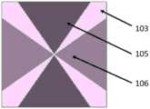
所述第一天线介质基板与第二天线介质基板交叉排列,第一天线介质基板在偶极子末端下方位置开槽,第二天线介质基板在偶极子末端上方位置开槽,完成两基板的对插;The first antenna dielectric substrate and the second antenna dielectric substrate are arranged crosswise, the first antenna dielectric substrate is slotted below the end of the dipole, and the second antenna dielectric substrate is slotted above the end of the dipole to complete the two substrates. plug;
进一步地,所述第一天线介质基板与第二天线介质基板的交叉处设置有加强偶极子强耦合作用的寄生结构。该结构包括介质基板及上面印刷的四个三角形贴片,分为两组作用于X极化与Y极化,该贴片与折叠偶极子贴片需保证电连接;Further, a parasitic structure for enhancing the strong coupling effect of dipoles is provided at the intersection of the first antenna dielectric substrate and the second antenna dielectric substrate. The structure includes a dielectric substrate and four triangular patches printed on it, which are divided into two groups for X polarization and Y polarization, and the patch and the folded dipole patch need to ensure electrical connection;
进一步地,所述宽角阻抗匹配层上表面均匀印刷有若干个椭圆超材料环,且每个超材料环均为周期性开口环形结构。Further, several elliptical metamaterial rings are uniformly printed on the upper surface of the wide-angle impedance matching layer, and each metamaterial ring is a periodic open ring structure.
进一步地,所述微带渐变线根据极化方向不同,有两种不同朝向,且它们与反射地板印刷与同一介质基板的正反两面。Further, the microstrip gradient lines have two different orientations according to different polarization directions, and they are printed on the front and back sides of the same dielectric substrate with the reflective floor.
本发明的有益效果为:本发明提供的双极化超宽带强耦合折叠偶极子相控阵天线采用Marchand巴伦进行馈电,通过在天线基板上的开槽巧妙设计了双极化单元排布方式,达到了很高的极化纯度;偶极子单元末端所加载的新型寄生结构则一定程度上加强了偶极子之间的耦合,达到拓展频带的效果;下方通过微带渐变线进行同轴与巴伦之间的阻抗变换,并通过不同的微带线朝向避让出足够的空间进行双极化设计;天线所采用的新型椭圆超材料宽角阻抗匹配层取代了以往较厚重的纯介质匹配层,达到了减轻天线重量,简化天线结构的目的;该天线与馈电巴伦一体印刷在介质基板上,加工简单,组装灵便,整体重量轻并且结构稳固。The beneficial effects of the present invention are as follows: the dual-polarized ultra-wideband strong-coupling folded dipole phased array antenna provided by the present invention uses Marchand baluns for feeding, and the dual-polarization unit row is skillfully designed through the slot on the antenna substrate The distribution method achieves high polarization purity; the new parasitic structure loaded at the end of the dipole unit strengthens the coupling between the dipoles to a certain extent and achieves the effect of expanding the frequency band; the bottom is carried out through the microstrip gradient line. Impedance transformation between coaxial and balun, and avoid enough space for dual-polarization design through different microstrip line orientations; the new elliptical metamaterial wide-angle impedance matching layer used in the antenna replaces the previous thicker pure The dielectric matching layer achieves the purpose of reducing the weight of the antenna and simplifying the antenna structure; the antenna and the feeding balun are integrally printed on the dielectric substrate, which is simple in processing, flexible in assembly, light in overall weight and stable in structure.
附图说明Description of drawings
图1为本发明提供的电磁超材料加载的双极化强耦合超宽带相控阵天线单元结构示意图。FIG. 1 is a schematic structural diagram of a dual-polarized strong-coupling ultra-wideband phased array antenna unit loaded with electromagnetic metamaterials provided by the present invention.
图2为本发明提供的实施例中沿Y极化方向折叠偶极子及相连巴伦结构示意图。FIG. 2 is a schematic diagram of the structure of the folded dipole and the connected balun along the Y polarization direction in the embodiment provided by the present invention.
图3为本发明提供的实施例中偶极子末端交叉处寄生结构俯视图。FIG. 3 is a top view of the parasitic structure at the intersection of the ends of the dipoles in the embodiment provided by the present invention.
图4为本发明提供的实施例中所加载的椭圆环形超材料宽角阻抗匹配层示意图。FIG. 4 is a schematic diagram of an elliptical annular metamaterial wide-angle impedance matching layer loaded in an embodiment provided by the present invention.
图5为本发明提供的实施例中天线底部微带渐变线结构示意图。FIG. 5 is a schematic structural diagram of the microstrip gradient line at the bottom of the antenna in the embodiment provided by the present invention.
图6为本发明提供的实施例中图1双极化单元其中一个端口E面及H面0-45度扫描驻波情况。FIG. 6 is a situation of scanning standing waves at 0-45 degrees on the E-plane and H-plane of one port of the dual-polarization unit in FIG. 1 according to the embodiment provided by the present invention.
图7为本发明提供的实施例中图1双极化单元其中一个端口E面及H面0-45度全频段交叉极化情况。FIG. 7 shows the cross-polarization of one port E-plane and H-plane of 0-45 degrees in the full frequency band of the dual-polarization unit of FIG. 1 in the embodiment provided by the present invention.
图8为本发明提供的实施例中单元组成8X8面阵后,2GHz处0度、45度方位面和俯仰面的扫描方向图及交叉极化情况。FIG. 8 is a scanning pattern and cross-polarization of the azimuth plane and the elevation plane at 2 GHz at 0° and 45° after the units form an 8×8 area array in the embodiment provided by the present invention.
图9为本发明提供的实施例中单元组成8X8面阵后,1GHz处0度、45度方位面和俯仰面的扫描方向图及交叉极化情况。FIG. 9 is a scanning pattern and cross-polarization of the azimuth plane and the elevation plane at 1 GHz at 0° and 45° after the units form an 8×8 area array in the embodiment provided by the present invention.
图10为本发明提供的实施例中单元组成8X8面阵后,0.35GHz处0度、45度方位面和俯仰面的扫描方向图及交叉极化情况。FIG. 10 shows the scanning pattern and cross-polarization of the azimuth plane and the elevation plane at 0.35 GHz at 0.35 GHz after the units form an 8×8 area array in the embodiment provided by the present invention.
其中:1、强耦合折叠偶极子单元;2、宽角阻抗匹配层;3、馈电巴伦;4、微带渐变线;5、反射地板;101、第一天线介质基板;102、第二天线介质基板;103、加强耦合的寄生结构;104、双极化开槽;105、沿X极化方向加强耦合的寄生贴片;106、沿Y极化方向加强耦合的寄生贴片;201、椭圆超材料环;301、巴伦馈电部分;302、巴伦耦合部分;401、沿Y极化方向微带渐变线;402、沿X极化方向微带渐变线。Among them: 1. Strongly coupled folded dipole unit; 2. Wide-angle impedance matching layer; 3. Feed balun; 4. Microstrip gradient line; 5. Reflective floor; 101. The first antenna dielectric substrate; 102. Two-antenna dielectric substrate; 103. Parasitic structure for enhanced coupling; 104. Dual polarization slotting; 105. Parasitic patch for enhanced coupling along the X polarization direction; 106. Parasitic patch for enhanced coupling along the Y polarization direction; 201 , elliptical metamaterial ring; 301, balun feeding part; 302, balun coupling part; 401, microstrip gradient line along the Y polarization direction; 402, microstrip gradient line along the X polarization direction.
具体实施方式Detailed ways
下面对本发明的具体实施方式进行描述,以便于本技术领域的技术人员理解本发明,但应该清楚,本发明不限于具体实施方式的范围,对本技术领域的普通技术人员来讲,只要各种变化在所附的权利要求限定和确定的本发明的精神和范围内,这些变化是显而易见的,一切利用本发明构思的发明创造均在保护之列。The specific embodiments of the present invention are described below to facilitate those skilled in the art to understand the present invention, but it should be clear that the present invention is not limited to the scope of the specific embodiments. For those of ordinary skill in the art, as long as various changes Such changes are obvious within the spirit and scope of the present invention as defined and determined by the appended claims, and all inventions and creations utilizing the inventive concept are within the scope of protection.
如图1所示,一种电磁超材料加载的双极化强耦合超宽带相控阵天线,包括强耦合折叠偶极子单元1、宽角阻抗匹配层2、馈电巴伦3、微带渐变线4和反射地板5;所述强耦合折叠偶极子单元1与馈电巴伦3一体集成于同一介质基板,所述宽角阻抗匹配层2设置于强耦合折叠偶极子单元1顶部,且与反射地板5平行,所述微带渐变线4与馈电巴伦3相连,保证电连接,且与反射地板平行。As shown in Figure 1, a dual-polarized strong-coupling ultra-wideband phased array antenna loaded with electromagnetic metamaterials includes a strong-coupling folded dipole unit 1, a wide-angle impedance matching
如图2至图5所示,强耦合折叠偶极子单元1包括作用于Y极化方向的第一天线介质基板101、作用于X极化方向的第二天线介质基板102以及加强耦合的寄生结构103。其中,第一天线介质基板及第二天线介质基板末端加工有双极化开槽104,以便双极化天线的组装。需要注意的是,每个单元的偶极子贴片与阵列中的下一个单元并没有电连接,二者间有一个间隙来产生达到宽带特性的强耦合效应。在第一天线介质基板101与第二天线介质基板102相交的部分,下方设置有加强耦合的寄生结构103,该结构包含介质基板,以及印刷于其上的沿X极化方向加强耦合的寄生贴片105,沿Y极化方向加强耦合的寄生贴片106。两组贴片需要分别与偶极子进行电连接,从而提高偶极子单元之间的电容分量,加强耦合特性,满足天线的宽带需求。As shown in FIG. 2 to FIG. 5 , the strongly coupled folded dipole unit 1 includes a first antenna
以第一天线介质基板101为例,其上印刷有偶极子贴片,并在下方与馈电巴伦3一体集成。馈电巴伦采用Marchand巴伦形式,该巴伦包含与下方微带渐变线4相连的巴伦馈电部分301,印制于与偶极子相反的一侧,以及巴伦耦合部分302,印制于与偶极子相同的一侧。该巴伦实现了馈电端与天线端的匹配。Taking the first antenna
在整个天线的最上方,设置有采用新型椭圆超材料结构的宽角阻抗匹配层2,其上表面均匀印刷有若干个椭圆超材料环201,每个超材料环201均为椭圆周期性开口环形结构,该椭圆超材料环201结构以较薄的基板及独特的周期性结构,克服了传统宽角阻抗匹配层重量较重,加工时易留有缝隙等实际问题,实现了天线的轻量化以及模块化。On the top of the entire antenna, a wide-angle
在天线下方,同轴接头与馈电巴伦3之间,设置有一段弯折微带渐变线4。同样由于极化方向不同,为避让出足够的加工空间,分为沿Y极化方向微带渐变线401与沿X极化方向微带渐变线402。以沿Y极化方向微带渐变线401为例,与同轴接头接触的一端微带线较宽,代表阻抗越小,基本等于50欧姆,到渐变线的末端与馈电巴伦相接触时,微带线越来越窄,代表阻抗越大,基本等于100欧姆。弯折的设计使得变换线的实际长度很长,保证了变换的稳定性。在微带线的弯折处倒出了圆角,避免出现变换时的不连续性。Below the antenna, between the coaxial joint and the feeding
在以上结构中,天线介质基板、巴伦介质基板、增强耦合的寄生结构、宽角阻抗匹配层以及微带渐变线基板都采用Taconic-TLY,介电常数为2.2,其中微带渐变线基板的另一侧全部覆有金属,既作为微带弯折线的地板,又作为整个天线的反射地板。在加工组装时,地板上需开出相应位置及大小的槽让天线及巴伦介质基板穿过,之后通过焊接进行固定。In the above structure, the antenna dielectric substrate, the balun dielectric substrate, the parasitic structure for enhanced coupling, the wide-angle impedance matching layer and the microstrip gradient line substrate all use Taconic-TLY, and the dielectric constant is 2.2. The other side is fully covered with metal, serving both as a floor for the microstrip zigzag line and as a reflection floor for the entire antenna. When processing and assembling, the corresponding position and size of the slot should be opened on the floor to allow the antenna and the balun dielectric substrate to pass through, and then fixed by welding.
需要说明的是,若高频元件阵元间距等于其最高频率的半波长,则在整个工作频带内扫描到任何角度(除了±90度),皆不会产生栅瓣。为了尽可能在保证天线性能的情况下,不减小天线辐射口径,以达到更大的增益。因此,本发明中相控阵天线整体高度为0.45个高频波长,相邻偶极子单元之间的距离为对应频段最高频处的0.45波长。It should be noted that if the high-frequency element array element spacing is equal to the half-wavelength of its highest frequency, no grating lobes will be generated when scanning to any angle (except ±90 degrees) in the entire operating frequency band. In order to ensure the antenna performance as much as possible, the radiation aperture of the antenna is not reduced to achieve greater gain. Therefore, in the present invention, the overall height of the phased array antenna is 0.45 high-frequency wavelengths, and the distance between adjacent dipole units is 0.45 wavelengths at the highest frequency of the corresponding frequency band.
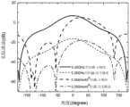
图6给出了本实施例在E面和H面不同扫描状态下的端口对应驻波特性,从图中可见,在驻波比要求小于3.2的情况下,双层介质基板对拓偶极子超宽带相控阵在45度扫描范围内具有接近7:1的阻抗带宽。(由于此双极化天线两个端口在结构上完全对称,因此以下图例都只给出其中一个端口的情况)Figure 6 shows the corresponding standing wave characteristics of the ports in the different scanning states of the E and H planes of this embodiment. It can be seen from the figure that when the standing wave ratio is less than 3.2, the double-layer dielectric substrate is used for the topography of the dipole. The sub-UWB phased array has an impedance bandwidth close to 7:1 over a 45-degree scan range. (Because the two ports of this dual-polarized antenna are completely symmetrical in structure, the following illustrations only show the case of one of the ports)
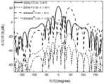
图7给出了本实施例在E面和H面不同扫描状态下的端口所有频率对应的交叉极化特性,从图中可见,天线在整个工作频段内交叉极化性能都可以在-30dB以下,此性能优于大多数强耦合天线。Figure 7 shows the cross-polarization characteristics corresponding to all frequencies of the port under different scanning states of the E-plane and H-plane of this embodiment. It can be seen from the figure that the cross-polarization performance of the antenna in the entire working frequency band can be below -30dB , which outperforms most strongly coupled antennas.
图8给出了本实施例所提供的8X8面阵,在2GHz频点处0度以及45度扫描的情况下的主极化与交叉极化情况。从图中可见,双层介质基板对拓偶极子超宽带相控阵具有30dB以上的交叉极化特性,并且该阵列主极化可达到22dB,主副瓣比可达到13dB以上。FIG. 8 shows the main polarization and cross-polarization of the 8×8 area array provided in this embodiment in the case of 0-degree and 45-degree scanning at the 2GHz frequency point. It can be seen from the figure that the double-layer dielectric substrate has a cross-polarization characteristic of more than 30dB for the dipole ultra-wideband phased array, and the main polarization of the array can reach 22dB, and the main-side lobe ratio can reach more than 13dB.
图9给出了本实施例所提供的8X8面阵,在1GHz频点处0度以及45度扫描的情况下的主极化与交叉极化情况。从图中可见,本实施例的双层介质基板对拓偶极子超宽带相控阵具有35dB以上的交叉极化特性;并且该阵列主极化增益可达到20dB,主副瓣比可达到13dB以上。FIG. 9 shows the main polarization and cross-polarization of the 8×8 area array provided by the present embodiment in the case of scanning 0 degrees and 45 degrees at the 1 GHz frequency point. It can be seen from the figure that the double-layer dielectric substrate anti-dipole ultra-wideband phased array in this embodiment has a cross-polarization characteristic of more than 35dB; and the main polarization gain of the array can reach 20dB, and the main-side lobe ratio can reach 13dB. above.
图10给出了本实施例所提供的8X8面阵,在0.35GHz频点处0度以及45度扫描的情况下的主极化与交叉极化情况;同样具有良好的交叉极化特性及波束扫描特性。Figure 10 shows the main polarization and cross-polarization of the 8X8 area array provided by this embodiment, in the case of 0-degree and 45-degree scanning at the 0.35GHz frequency point; it also has good cross-polarization characteristics and beams Scan characteristics.
Claims (2)
Priority Applications (1)
| Application Number | Priority Date | Filing Date | Title |
|---|---|---|---|
| CN201910386194.6ACN110323575B (en) | 2019-05-09 | 2019-05-09 | Dual-polarized strongly coupled ultra-wideband phased array antenna loaded with electromagnetic metamaterials |
Applications Claiming Priority (1)
| Application Number | Priority Date | Filing Date | Title |
|---|---|---|---|
| CN201910386194.6ACN110323575B (en) | 2019-05-09 | 2019-05-09 | Dual-polarized strongly coupled ultra-wideband phased array antenna loaded with electromagnetic metamaterials |
Publications (2)
| Publication Number | Publication Date |
|---|---|
| CN110323575A CN110323575A (en) | 2019-10-11 |
| CN110323575Btrue CN110323575B (en) | 2020-07-28 |
Family
ID=68118903
Family Applications (1)
| Application Number | Title | Priority Date | Filing Date |
|---|---|---|---|
| CN201910386194.6AActiveCN110323575B (en) | 2019-05-09 | 2019-05-09 | Dual-polarized strongly coupled ultra-wideband phased array antenna loaded with electromagnetic metamaterials |
Country Status (1)
| Country | Link |
|---|---|
| CN (1) | CN110323575B (en) |
Families Citing this family (23)
| Publication number | Priority date | Publication date | Assignee | Title |
|---|---|---|---|---|
| CN111313159B (en)* | 2019-12-27 | 2021-07-16 | 中国航空工业集团公司西安飞机设计研究所 | A method for optimizing the impedance characteristics of an airborne electric small short-wave antenna and a broadband short-wave antenna |
| CN111293413B (en)* | 2020-03-03 | 2021-02-05 | 电子科技大学 | A compact wideband filter antenna and its MIMO antenna based on cross-coupling structure |
| CN111370860B (en)* | 2020-03-10 | 2021-01-26 | 电子科技大学 | Strong coupling ultra wide band phased array antenna based on interdigital resistive surface loading |
| CN111697331B (en)* | 2020-06-22 | 2024-03-22 | 东南大学 | Ultra-wideband tightly coupled antenna array and antenna equipment |
| CN111710966B (en)* | 2020-06-30 | 2022-05-06 | 广东工业大学 | Split ring loaded dual-frequency dual-polarized base station antenna |
| CN112038753B (en)* | 2020-08-31 | 2021-05-14 | 电子科技大学 | Conformal dual-polarized strong-coupling ultra-wideband dipole phased array of thin wing |
| CN112310649B (en)* | 2020-11-09 | 2021-07-16 | 电子科技大学 | Ultra-low-profile, low-scattering, and ultra-broadband phased array based on electromagnetic metamaterial loading |
| CN112490650B (en)* | 2020-11-12 | 2022-09-23 | 杭州电子科技大学 | An Impedance Matching Method for Low Profile Ultra-Wideband Array Antennas |
| CN112701471B (en)* | 2020-11-27 | 2022-06-03 | 电子科技大学 | All-dielectric integrated ultra-wideband low-profile polymorphic conformal phased array antenna |
| CN112864617B (en)* | 2021-01-12 | 2022-04-08 | 西安电子科技大学 | 5G millimeter-wave dual-polarized wide-bandwidth angle tightly coupled array antenna |
| CN112952374B (en)* | 2021-01-28 | 2021-10-22 | 电子科技大学 | Ferrite-loaded dual-polarized low-profile strong-coupling ultra-wideband phased array antenna |
| KR20220137487A (en)* | 2021-04-02 | 2022-10-12 | 삼성전자주식회사 | Antenna module and electronic device including the same |
| CN113871865A (en)* | 2021-08-24 | 2021-12-31 | 西安电子科技大学 | A Low Profile Wide Bandwidth Two-Dimensional Scanning Dual-Polarized Phased Array Antenna and Its Application |
| CN114156627B (en)* | 2021-10-29 | 2023-02-10 | 电子科技大学 | An Ultra-Wideband Low Profile Low Scattering Curved Phased Array Antenna |
| CN114069257B (en)* | 2021-11-17 | 2022-07-26 | 中国人民解放军国防科技大学 | An ultra-wideband dual-polarized phased array antenna based on strongly coupled dipoles |
| CN114142207B (en)* | 2021-11-30 | 2023-11-07 | 中国电子科技集团公司第十四研究所 | Foldable large-spacing ultra-wideband low-profile tightly-coupled array antenna |
| CN114284751B (en)* | 2021-12-13 | 2024-04-16 | 中国电子科技集团公司第三十八研究所 | A large-spacing ultra-wideband tightly coupled dipole array antenna with integrated correction network |
| CN115084873B (en)* | 2022-03-08 | 2025-01-03 | 电子科技大学 | A dual-polarized 1-bit antenna and digital bit array based on electromagnetic metamaterials |
| CN114566798A (en)* | 2022-03-31 | 2022-05-31 | 电子科技大学 | Low-profile dual-polarized strong-coupling ultra-wideband full-wing conformal dipole phased array antenna |
| CN114744409B (en)* | 2022-04-13 | 2023-01-24 | 电子科技大学 | Ten-fold frequency-range dual-polarized strong-coupling phased array antenna loaded by resistive material |
| CN114725685B (en)* | 2022-04-27 | 2024-03-01 | 东南大学 | Planar tight coupling ultra-wideband phased array based on transverse connection folded dipole |
| CN116417794B (en)* | 2023-04-02 | 2024-07-19 | 深圳汉阳天线设计有限公司 | High-isolation MIMO antenna |
| CN119297618B (en)* | 2024-12-11 | 2025-03-21 | 西安电子科技大学 | A tightly coupled array antenna based on integrated microstrip balun |
Citations (4)
| Publication number | Priority date | Publication date | Assignee | Title |
|---|---|---|---|---|
| CN102394349A (en)* | 2011-07-08 | 2012-03-28 | 电子科技大学 | Octagonal-ring plane bipolarized broadband phased-array antenna based on strong mutual coupling effects |
| CN108598691A (en)* | 2018-04-02 | 2018-09-28 | 电子科技大学 | Scanning Phased Array Antenna with Broadband based on the long slot antenna of tablet |
| CN109273834A (en)* | 2018-08-29 | 2019-01-25 | 电子科技大学 | Ultra-wideband strong mutual coupling phased array antenna based on grounded metal strip |
| CN109687108A (en)* | 2018-12-25 | 2019-04-26 | 电子科技大学 | A kind of low section broadband and wideangle phased array antenna of big unit spacing |
Family Cites Families (5)
| Publication number | Priority date | Publication date | Assignee | Title |
|---|---|---|---|---|
| US6512487B1 (en)* | 2000-10-31 | 2003-01-28 | Harris Corporation | Wideband phased array antenna and associated methods |
| US10516214B2 (en)* | 2013-11-05 | 2019-12-24 | Si2 Technologies, Inc. | Antenna elements and array |
| US10158179B2 (en)* | 2016-04-06 | 2018-12-18 | Phase Sensitive Innovations, Inc. | Phased-array antenna with in-plane optical feed and method of manufacture |
| CN108493625B (en)* | 2018-03-12 | 2019-09-20 | 电子科技大学 | Improved low-profile low-scattering strong-coupling ultra-broadband phased array |
| CN109494464B (en)* | 2018-11-12 | 2019-07-26 | 电子科技大学 | A Low Cross-Polarization Ultra-Broadband Strongly Coupling Antipodal Dipole Phased Array Antenna |
- 2019
- 2019-05-09CNCN201910386194.6Apatent/CN110323575B/enactiveActive
Patent Citations (4)
| Publication number | Priority date | Publication date | Assignee | Title |
|---|---|---|---|---|
| CN102394349A (en)* | 2011-07-08 | 2012-03-28 | 电子科技大学 | Octagonal-ring plane bipolarized broadband phased-array antenna based on strong mutual coupling effects |
| CN108598691A (en)* | 2018-04-02 | 2018-09-28 | 电子科技大学 | Scanning Phased Array Antenna with Broadband based on the long slot antenna of tablet |
| CN109273834A (en)* | 2018-08-29 | 2019-01-25 | 电子科技大学 | Ultra-wideband strong mutual coupling phased array antenna based on grounded metal strip |
| CN109687108A (en)* | 2018-12-25 | 2019-04-26 | 电子科技大学 | A kind of low section broadband and wideangle phased array antenna of big unit spacing |
Non-Patent Citations (2)
| Title |
|---|
| Analysis and Characterization of a Wide-Angle Impedance Matching Metasurface for Dipole Phased Arrays;Trevor R. Cameron等;《IEEE Transactions on Antennas and Propagation》;20150622;全文* |
| Utilization of metamaterials for wide angle impedance matching (WAIM) in phased array antennas;Soji Sajuyigbe等;《2009 IEEE Antennas and Propagation Society International Symposium》;20090724;全文* |
Also Published As
| Publication number | Publication date |
|---|---|
| CN110323575A (en) | 2019-10-11 |
Similar Documents
| Publication | Publication Date | Title |
|---|---|---|
| CN110323575B (en) | Dual-polarized strongly coupled ultra-wideband phased array antenna loaded with electromagnetic metamaterials | |
| CN111370860B (en) | Strong coupling ultra wide band phased array antenna based on interdigital resistive surface loading | |
| CN109494464B (en) | A Low Cross-Polarization Ultra-Broadband Strongly Coupling Antipodal Dipole Phased Array Antenna | |
| CN110085975B (en) | Wing-borne low-scattering ultra-wideband conformal phased array based on strong coupling effect | |
| CN115084872B (en) | Ultra-wide bandwidth scanning angle tight coupling phased array antenna | |
| CN112952374B (en) | Ferrite-loaded dual-polarized low-profile strong-coupling ultra-wideband phased array antenna | |
| CN114744409B (en) | Ten-fold frequency-range dual-polarized strong-coupling phased array antenna loaded by resistive material | |
| CN110707421A (en) | Dual-polarization tightly-coupled phased array antenna based on end overlapping | |
| CN114156627B (en) | An Ultra-Wideband Low Profile Low Scattering Curved Phased Array Antenna | |
| CN112234365B (en) | Checkerboard Low Scattering Low Profile Strong Mutual Coupling Broadband Planar Phased Array | |
| CN113690636B (en) | Millimeter wave wide-angle scanning phased-array antenna based on super surface | |
| CN111969335B (en) | Conformal dual-polarized two-dimensional single-pulse end-fire array antenna | |
| CN110380193A (en) | A kind of miniaturization multiband Shared aperture circular polarized antenna | |
| CN110233336B (en) | Series-fed circularly polarized antenna normal array | |
| CN113764879A (en) | A low-profile ultra-wideband antenna based on a resistive metasurface | |
| CN111430936A (en) | 5G MIMO multi-beam antenna based on super surface | |
| CN112038753B (en) | Conformal dual-polarized strong-coupling ultra-wideband dipole phased array of thin wing | |
| CN115810917A (en) | Satellite-borne Ka-band circularly polarized antenna unit, antenna array and phased array | |
| CN114069257A (en) | Ultra-wideband dual-polarized phased array antenna based on strong coupling dipoles | |
| CN108134203B (en) | Large-unit-space wide-angle scanning phased array antenna based on electromagnetic band gap structure | |
| CN112117532A (en) | Compact low-coupling triple-polarization backtracking array and triple-polarization MIMO antenna unit based on microstrip antenna | |
| CN116565557A (en) | A wide-angle scanning ultra-wideband dual-polarization phased array antenna | |
| CN112701494A (en) | All-dielectric integrated planar ultra-wideband low-profile wide-angle scanning phased array antenna | |
| CN116937181A (en) | Ultra-wide bandwidth angle scanning antenna array based on tightly coupled dipole units | |
| CN119050642B (en) | Ferrite-loaded large curvature wing conformal strongly coupled ultra-wideband one-dimensional phased array antenna |
Legal Events
| Date | Code | Title | Description |
|---|---|---|---|
| PB01 | Publication | ||
| PB01 | Publication | ||
| SE01 | Entry into force of request for substantive examination | ||
| SE01 | Entry into force of request for substantive examination | ||
| GR01 | Patent grant | ||
| GR01 | Patent grant |