CN110320663B - Design of Ultra-Small Size Large Bandwidth Mode Filter Based on Direct Binary Search Algorithm - Google Patents
Design of Ultra-Small Size Large Bandwidth Mode Filter Based on Direct Binary Search AlgorithmDownload PDFInfo
- Publication number
- CN110320663B CN110320663BCN201910212740.4ACN201910212740ACN110320663BCN 110320663 BCN110320663 BCN 110320663BCN 201910212740 ACN201910212740 ACN 201910212740ACN 110320663 BCN110320663 BCN 110320663B
- Authority
- CN
- China
- Prior art keywords
- waveguide
- objective function
- search algorithm
- binary search
- scanning
- Prior art date
- Legal status (The legal status is an assumption and is not a legal conclusion. Google has not performed a legal analysis and makes no representation as to the accuracy of the status listed.)
- Expired - Fee Related
Links
- 238000010845search algorithmMethods0.000titleclaimsabstractdescription15
- 238000002834transmittanceMethods0.000claimsabstractdescription17
- 238000004080punchingMethods0.000claimsabstractdescription7
- 238000000034methodMethods0.000claimsdescription12
- 238000004519manufacturing processMethods0.000abstractdescription5
- 238000001914filtrationMethods0.000abstractdescription4
- 238000010586diagramMethods0.000description11
- VYPSYNLAJGMNEJ-UHFFFAOYSA-NSilicium dioxideChemical groupO=[Si]=OVYPSYNLAJGMNEJ-UHFFFAOYSA-N0.000description3
- XUIMIQQOPSSXEZ-UHFFFAOYSA-NSiliconChemical compound[Si]XUIMIQQOPSSXEZ-UHFFFAOYSA-N0.000description3
- 230000005540biological transmissionEffects0.000description3
- 238000004891communicationMethods0.000description3
- 238000005516engineering processMethods0.000description3
- 230000003287optical effectEffects0.000description3
- 229910052710siliconInorganic materials0.000description3
- 239000010703siliconSubstances0.000description3
- 238000006243chemical reactionMethods0.000description2
- 238000005253claddingMethods0.000description2
- 239000010410layerSubstances0.000description2
- 239000000463materialSubstances0.000description2
- 238000005457optimizationMethods0.000description2
- 230000000717retained effectEffects0.000description2
- OKTJSMMVPCPJKN-UHFFFAOYSA-NCarbonChemical compound[C]OKTJSMMVPCPJKN-UHFFFAOYSA-N0.000description1
- 230000032823cell divisionEffects0.000description1
- 230000007812deficiencyEffects0.000description1
- 238000005530etchingMethods0.000description1
- 238000004880explosionMethods0.000description1
- 229910021389grapheneInorganic materials0.000description1
- 239000012212insulatorSubstances0.000description1
- 230000010354integrationEffects0.000description1
- 239000002070nanowireSubstances0.000description1
- 239000013307optical fiberSubstances0.000description1
- 239000004038photonic crystalSubstances0.000description1
- 238000000623plasma-assisted chemical vapour depositionMethods0.000description1
- 235000012239silicon dioxideNutrition0.000description1
- 239000000377silicon dioxideSubstances0.000description1
- 229910052814silicon oxideInorganic materials0.000description1
- 239000002356single layerSubstances0.000description1
- 239000000758substrateSubstances0.000description1
- 238000000411transmission spectrumMethods0.000description1
Images


Classifications
- G—PHYSICS
- G02—OPTICS
- G02B—OPTICAL ELEMENTS, SYSTEMS OR APPARATUS
- G02B27/00—Optical systems or apparatus not provided for by any of the groups G02B1/00 - G02B26/00, G02B30/00
- G02B27/0012—Optical design, e.g. procedures, algorithms, optimisation routines
- G—PHYSICS
- G02—OPTICS
- G02B—OPTICAL ELEMENTS, SYSTEMS OR APPARATUS
- G02B6/00—Light guides; Structural details of arrangements comprising light guides and other optical elements, e.g. couplings
- G02B6/10—Light guides; Structural details of arrangements comprising light guides and other optical elements, e.g. couplings of the optical waveguide type
- G02B6/12—Light guides; Structural details of arrangements comprising light guides and other optical elements, e.g. couplings of the optical waveguide type of the integrated circuit kind
Landscapes
- Physics & Mathematics (AREA)
- General Physics & Mathematics (AREA)
- Optics & Photonics (AREA)
- Engineering & Computer Science (AREA)
- Microelectronics & Electronic Packaging (AREA)
- Optical Integrated Circuits (AREA)
Abstract
Translated fromChinese
Description
Translated fromChinese技术领域technical field
本发明属于平面光波导集成器件,具体涉及一种基于直接二元搜索算法(简称DBS算法)设计的模式滤波器。The invention belongs to a plane optical waveguide integrated device, in particular to a mode filter designed based on a direct binary search algorithm (abbreviated as DBS algorithm).
背景技术Background technique
21世纪处于信息爆炸的时期,人们对于信息的需求量高速增长,对通信网络的带宽和容量也提出了更高的要求。为增大光通信系统的通信容量,多种复用技术应运而生。光纤中的空分复用(SDM)技术一直在迅速发展,以支持光传输容量的指数增长。作为该技术的片上集成,硅基集成的模分复用系统(MDM)由于其小尺寸、与CMOS制造工艺兼容、以及与目前已成熟的波分复用系统(WDM)的扩展性而引起了广泛关注。The 21st century is in a period of information explosion. People's demand for information is growing rapidly, and higher requirements are also placed on the bandwidth and capacity of communication networks. In order to increase the communication capacity of the optical communication system, a variety of multiplexing technologies emerge as the times require. Spatial division multiplexing (SDM) technology in optical fibers has been rapidly evolving to support the exponential growth in optical transmission capacity. As the on-chip integration of this technology, silicon-based integrated mode division multiplexing (MDM) systems have attracted attention due to their small size, compatibility with CMOS fabrication processes, and scalability with the now well-established wavelength division multiplexing (WDM) systems. extensive attention.
模分复用系统中,模式滤波器是一个必不可少的器件,用于滤除不需要的模式,只允许设计所需求的模式通过,类似波分复用系统中的波长滤波器的功能。在多模波导中,由于其对高阶模限制较弱,因此滤除其中的高阶模而只保留低阶模有很多简单的解决方案,例如,将波导逐渐变细到高阶模式的截止宽度,或者在适当设计的波导弯曲中滤除高阶模式。然而,在多模波导中只滤除低阶模式而让高阶模式通过的滤波器是比较难以实现的。In the mode division multiplexing system, the mode filter is an indispensable device, which is used to filter out the unwanted mode and allow only the mode required by the design to pass, similar to the function of the wavelength filter in the wavelength division multiplexing system. In multimode waveguides, because of their weak confinement to higher-order modes, there are many simple solutions to filter out higher-order modes and keep only lower-order modes, such as tapering the waveguide to the cutoff width of higher-order modes, or in Higher order modes are filtered out in properly designed waveguide bends. However, in a multimode waveguide, a filter that only filters out low-order modes and passes higher-order modes is more difficult to implement.
目前针对高阶模式滤波器,已有多种方案被提出。2015年,XIAOWEI GUAN等人利用一维光子晶体实现了高阶模滤波器;2016年,Y.TANG等人利用双曲线超材料作为波导包层,使波导只支持高阶TM模式;2017年,ZESHAN CHANG等人在波导中埋入单层石墨烯,使高阶模传输时损耗较低,而低阶模传输有很大的损耗;2017年,KAZI TANVIR AHMMED等人利用MZI实现模式转换,先将TE0和TE1相互转换,滤波之后,再将模式转换成初始状态,2018年,CHUNLEI SUN等人在此基础上给MZI臂上加上热电极,实现可调控的模式滤波功能。此外,模式解复用器也可以被看成是模式滤波器,但是它们一般都存在尺寸过大的弊端。At present, for high-order mode filters, a variety of schemes have been proposed. In 2015, XIAOWEI GUAN et al. realized high-order mode filters using one-dimensional photonic crystals; in 2016, Y.TANG et al. used hyperbolic metamaterials as the waveguide cladding, so that the waveguide only supports high-order TM modes; in 2017, ZESHAN CHANG et al. buried single-layer graphene in the waveguide, so that the loss of high-order mode transmission is low, while the transmission of low-order mode has a large loss; in 2017, KAZI TANVIR AHMMED et al. used MZI to achieve mode conversion, first TE0 and TE1 After mutual conversion and filtering, the mode is converted to the initial state. In 2018, CHUNLEI SUN et al. added a thermode to the MZI arm on this basis to realize the adjustable mode filtering function. In addition, mode demultiplexers can also be thought of as mode filters, but they generally suffer from oversize.
因此,目前的模式滤波器都有着工艺复杂、尺寸较大、工作带宽窄等缺点。Therefore, the current mode filters all have the disadvantages of complex process, large size, and narrow operating bandwidth.
发明内容SUMMARY OF THE INVENTION
本发明所要解决的技术问题是克服现有模式滤波器工艺复杂、器件尺寸大、带宽窄等技术不足,提供一种新的基于DBS算法设计的模式滤波器。The technical problem to be solved by the present invention is to overcome the technical deficiencies of the existing mode filter, such as complicated process, large device size and narrow bandwidth, and to provide a new mode filter designed based on the DBS algorithm.
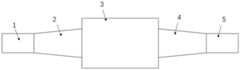
为解决上述技术问题,本发明提供一种基于DBS算法设计的模式滤波器,包括输入波导(1)、输入锥形结构(2)、优化波导区域(3)、输出锥形结构(4)、输出波导(5);In order to solve the above technical problems, the present invention provides a mode filter designed based on a DBS algorithm, comprising an input waveguide (1), an input tapered structure (2), an optimized waveguide region (3), an output tapered structure (4), output waveguide (5);
优化波导区域被划分成若干个正方形单元格,每一个单元格的状态为不打孔或正中心圆孔;每一个单元格的状态的确定方式是:根据DBS算法和设置的目标函数,计算每一个单元格的状态,以使目标函数达到最大值。The optimized waveguide area is divided into several square cells, and the state of each cell is no punching or a center hole; the state of each cell is determined by: according to the DBS algorithm and the set objective function, calculate each The state of a cell such that the objective function reaches its maximum value.
所述优化波导区域的尺寸为所划分正方形单元格边长的整数倍。The size of the optimized waveguide region is an integer multiple of the side length of the divided square unit cells.
优选的,所划分的正方形单元格边长a满足Preferably, the side length a of the divided square cells satisfies

式中,λ为优化中心波长,neff为波导有效折射率;where λ is the optimal center wavelength, and neff is the effective refractive index of the waveguide;
正中心圆孔的直径d满足80nm≤d≤(a-30nm)。The diameter d of the central hole satisfies 80nm≤d≤(a-30nm).
进一步的,所述输入锥形结构的宽度大的一端与优化波导区域相连,宽度小的一端与输入波导相连;所述输出锥形结构波导宽度大的一端与优化波导区域相连,宽度小的一端与输出波导相连。该锥形结构可以增加器件制作的工艺容差性,并滤除可能产生的高阶模式。Further, the large width end of the input tapered structure is connected to the optimized waveguide region, and the small width end is connected to the input waveguide; the output tapered structure waveguide has a large width end connected to the optimized waveguide region, and the small width end is connected to the optimized waveguide region. connected to the output waveguide. The tapered structure can increase the process tolerance of device fabrication and filter out possible higher-order modes.
所述根据DBS算法和设置的目标函数,计算每一个单元格的状态,以使目标函数达到最大值的步骤包括:依次扫描优化波导区域每一个单元格,改变扫描单元格的状态,计算当前目标函数,将当前目标函数与未改变该单元格状态时的目标函数值相比较,若当前目标函数值得到改善,则保留该扫描单元格的新状态,否则,将该单元格恢复原状态。The step of calculating the state of each cell according to the DBS algorithm and the set objective function, so that the objective function reaches the maximum value, includes: scanning each cell in the optimized waveguide region in turn, changing the state of the scanning cell, and calculating the current target The function compares the current objective function with the objective function value when the state of the cell is not changed. If the current objective function value is improved, the new state of the scanned cell is retained, otherwise, the cell is restored to the original state.
优选的,在使用DBS算法计算优化波导区域每一个单元格状态时,交替使用按行扫描和按列扫描的方式;按行扫描时在水平方向上从左往右,垂直方向上从下往上;按列扫描时在垂直方向上从下往上,水平方向上从左往右。Preferably, when using the DBS algorithm to calculate the state of each cell in the optimized waveguide region, alternately use scanning by row and scanning by column; when scanning by row, it is from left to right in the horizontal direction, and from bottom to top in the vertical direction. ; Scan in columns from bottom to top vertically and from left to right horizontally.
进一步包括:首先,设置目标函数中目标透过率与串扰占据相同比重,交替使用按行和按列扫描,直至目标函数收敛;然后,将目标函数中目标透过率与串扰的比重设置为1:10,在已有的最优解的基础上继续交替使用按行和按列扫描,直至目标函数收敛。It further includes: first, set the target transmittance and crosstalk to occupy the same proportion in the objective function, and alternately use row-by-row and column-by-column scanning until the objective function converges; then, set the proportion of target transmittance and crosstalk in the objective function to 1 : 10, continue to use row-by-row and column-by-column scanning alternately on the basis of the existing optimal solution until the objective function converges.
目标函数收敛的判断依据为扫描完一轮优化波导区域所有单元格后,目标函数的改变值低于0.1%。The criterion for the convergence of the objective function is that the change value of the objective function is less than 0.1% after scanning all cells in the optimized waveguide region.
本发明的基于DBS算法设计的模式滤波器,用于实现模式滤波的功能,当输入波导入射的TE1模式经过优化波导区域,能保持很高的透过率被输出波导接收;而输入波导入射的TE0模式经过优化波导区域中多个小孔的衍射,能量从波导侧面发散出去,无法被输出波导接收。The mode filter designed based on the DBS algorithm of the present invention is used to realize the function of mode filtering. When the TE1 mode introduced by the input waveguide passes through the optimized waveguide area, it can maintain a high transmittance and be received by the output waveguide; The TE0 mode is optimized for diffraction by multiple small holes in the waveguide area, and the energy is diffused from the side of the waveguide and cannot be received by the output waveguide.
本发明的基于DBS算法设计的模式滤波器,解决了制作工艺步骤复杂以及器件尺寸过大的问题,实现了损耗低、带宽大、尺寸超小、一步刻蚀的模式滤波器。The mode filter designed based on the DBS algorithm of the present invention solves the problems of complex manufacturing process steps and excessive device size, and realizes a mode filter with low loss, large bandwidth, ultra-small size and one-step etching.
附图说明Description of drawings
下面结合附图和具体实施方式对本发明的技术方案作进一步具体说明。The technical solutions of the present invention will be further described in detail below with reference to the accompanying drawings and specific embodiments.
图1是本发明器件的三维结构示意图。FIG. 1 is a schematic diagram of the three-dimensional structure of the device of the present invention.
图2是本发明器件的二维平面结构示意图。FIG. 2 is a schematic diagram of a two-dimensional planar structure of the device of the present invention.
图3是本发明器件的未优化时的初始结构示意图。FIG. 3 is a schematic diagram of the initial structure of the device of the present invention when it is not optimized.
图4是本发明器件的优化波导区域单元格划分示意图。FIG. 4 is a schematic diagram of the optimized waveguide region cell division of the device of the present invention.
图5是本发明器件中单元格的两种状态,(a)为不打孔,(b)为正中心打圆孔。Fig. 5 shows two states of the cell in the device of the present invention, (a) without punching, (b) punching a circular hole in the center.
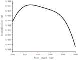
图6是本发明器件实例中TE1模式的透射谱。Figure 6 is a transmission spectrum of the TE1 mode in the device example of the present invention.
图7是本发明器件实例中T00、T01、T10三个串扰图。FIG. 7 is three crosstalk diagrams of T00 , T01 , and T10 in the device example of the present invention.
图中:1、输入波导,2、输入锥形结构,3、优化波导区域,4、输出锥形结构,5、输出波导。In the figure: 1. Input waveguide, 2. Input tapered structure, 3. Optimized waveguide area, 4. Output tapered structure, 5. Output waveguide.
具体实施方式Detailed ways
以下结合附图对本发明的具体实施进一步说明。The specific implementation of the present invention will be further described below with reference to the accompanying drawings.
本发明提出的是一种基于DBS算法设计模式滤波器,其三维结构示意图如图1所示,二维平面结构示意图如图2所示,包括输入波导1、输入锥形结构2、优化波导区域3、输出锥形结构4、输出波导5。The present invention proposes a mode filter based on the DBS algorithm, the schematic diagram of its three-dimensional structure is shown in Figure 1, and the schematic diagram of the two-dimensional plane structure is shown in Figure 2, including
优化波导区域被划分成若干个正方形单元格,每一个单元格的状态为不打孔或正中心圆孔;每一个单元格的状态的确定方式是:根据DBS算法和设置的目标函数,计算每一个单元格的状态,以使目标函数达到最大值。The optimized waveguide area is divided into several square cells, and the state of each cell is no punching or a center hole; the state of each cell is determined by: according to the DBS algorithm and the set objective function, calculate each The state of a cell such that the objective function reaches its maximum value.
优化波导区域的尺寸为所划分正方形单元格边长的整数倍。The size of the optimized waveguide region is an integer multiple of the side length of the divided square cells.
优选的,所划分的正方形单元格边长a满足Preferably, the side length a of the divided square cells satisfies

式中,λ为优化中心波长,neff为波导有效折射率;where λ is the optimized center wavelength, and neff is the effective refractive index of the waveguide;
正中心圆孔的直径d满足80nm≤d≤(a-30nm),以保证工艺上可以实现。The diameter d of the central circular hole satisfies 80nm≤d≤(a-30nm) to ensure that it can be realized in the process.
输入锥形结构的宽度大的一端与优化波导区域相连,宽度小的一端与输入波导相连;所述输出锥形结构波导宽度大的一端与优化波导区域相连,宽度小的一端与输出波导相连。该锥形结构可以增加器件制作的工艺容差性,并滤除可能产生的高阶模式。The large width end of the input tapered structure is connected to the optimized waveguide region, and the small width end is connected to the input waveguide; the large width end of the output tapered structure waveguide is connected to the optimized waveguide region, and the small width end is connected to the output waveguide. The tapered structure can increase the process tolerance of device fabrication and filter out possible higher-order modes.
未使用DBS算法优化前,其结构示意图如图3所示,优化区域是一段略宽于输入、输出波导的直波导。将优化波导区域划分成若干个正方形单元格,划分示意图如图4所示,以便于DBS算法依次扫描。每一个单元格有两种状态:不打孔和正中心圆孔,示意图如图5(a)和(b)所示。Before optimization using the DBS algorithm, the schematic diagram of its structure is shown in Figure 3. The optimization area is a straight waveguide that is slightly wider than the input and output waveguides. The optimized waveguide area is divided into several square cells, and the schematic diagram of the division is shown in Figure 4, so that the DBS algorithm can scan in sequence. Each cell has two states: no hole punching and center hole, as shown in Figure 5(a) and (b).
在使用DBS算法计算优化波导区域每一个单元格状态时,交替使用按行扫描和按列扫描的方式。按行扫描时在水平方向上从左往右,垂直方向上从下往上;按列扫描时在垂直方向上从下往上,水平方向上从左往右。依次扫描优化波导区域每一个单元格,改变扫描单元格的状态,计算目标函数,与未改变该单元格状态时的目标函数值相比较,若目标函数值得到改善,则保留该扫描单元格的新状态,否则,将该单元格恢复原状态。When using the DBS algorithm to calculate the state of each cell in the optimized waveguide region, the scanning by row and scanning by column are alternately used. When scanning by row, it is from left to right in the horizontal direction, and from bottom to top in the vertical direction; when scanning by column, it is from bottom to top in the vertical direction, and from left to right in the horizontal direction. Scan each cell in the optimized waveguide area in turn, change the state of the scanning cell, calculate the objective function, and compare it with the objective function value when the state of the cell is not changed. If the objective function value is improved, keep the value of the scanning cell. new state, otherwise, restore the cell to its original state.
在扫描过程中,共使用了两个目标函数。第一个目标函数为:During the scanning process, a total of two objective functions were used. The first objective function is:
FOM1=T11-(T00+T01+T10)FOM1 =T11 -(T00 +T01 +T10 )
其中,Tmn代表入射为TEm出射为TEn的透过率,即T11为目标透过率,T00、T01、T10均为串扰。该目标函数中,目标透过率与串扰占相同的比重,交替使用按行和按列扫描,直至目标函数收敛,随后使用第二个目标函数:Among them, Tmn represents the transmittance of the incident TEm and the output of TEn , that is, T11 is the target transmittance, and T00 , T01 , and T10 are all crosstalk. In this objective function, the target transmittance and crosstalk account for the same proportion. Scanning by row and column is alternately used until the objective function converges, and then the second objective function is used:
FOM2=T11-10×(T00+T01+T10)FOM2 =T11 -10×(T00 +T01 +T10 )
第二个目标函数中的目标透过率与串扰的比重变为了1:10,增加了串扰权重,以改善器件最终的串扰性能。在已有的最优解上继续交替使用按行和按列扫描,直至目标函数收敛。The ratio of the target transmittance to crosstalk in the second objective function is changed to 1:10, and the crosstalk weight is increased to improve the final crosstalk performance of the device. Continue to alternately use row-by-row and column-by-column scans on the existing optimal solution until the objective function converges.
经过若干轮扫描后,优化波导区域分布着若干个圆孔,输入波导入射的TE1模式经过优化波导区域,能保持很高的透过率被输出波导接收;而输入波导入射的TE0模式经过优化波导区域中多个小孔的衍射,能量从波导侧面发散出去,无法被输出波导接收。After several rounds of scanning, there are several circular holes distributed in the optimized waveguide area. The TE1 mode transmitted by the input waveguide can be received by the output waveguide with a high transmittance through the optimized waveguide area; while the TE0 mode transmitted by the input waveguide is optimized by the waveguide. Diffraction of multiple small holes in the area, the energy is diffused from the side of the waveguide and cannot be received by the output waveguide.
下面通过一个具体实施例来对本发明作进一步说明:The present invention will be further described below by a specific embodiment:
选用基于绝缘体上硅(SOI)材料的硅纳米线,顶层硅厚度为220nm,材料折射率为3.476,衬底为3μm厚的二氧化硅,折射率为1.444,上包层为PECVD工艺生长的二氧化硅,折射率为1.4575。Silicon nanowires based on silicon-on-insulator (SOI) materials are selected. The thickness of the top layer of silicon is 220 nm, the refractive index of the material is 3.476, the substrate is silicon dioxide with a thickness of 3 μm, the refractive index is 1.444, and the upper cladding layer is PECVD process growth. Silicon oxide with a refractive index of 1.4575.
设计一个基于DBS算法的模式滤波器,中心波长为1550nm,优化波长区间为100nm,工作模式为TE1和TE0模式。Design a mode filter based on DBS algorithm, the center wavelength is 1550nm, the optimized wavelength range is 100nm, and the working modes are TE1 and TE0 modes.
在具体实施案例中,采用以下的方法:In specific implementation cases, the following methods are used:
1.设置输入波导和输出波导的宽度均为0.6μm,确保其可以无损耗的支持TE0模式、TE1模式,同时更高阶模式如TE2均截止。输入、输出锥形结构的宽度则是从0.6μm过渡到0.9μm,长度为20μm,以保证TE0和TE1模式均绝热演化。优化波导区域尺寸为1.56μm×2.4μm。1. Set the width of the input waveguide and the output waveguide to be 0.6 μm to ensure that they can support TE0 mode and TE1 mode without loss, and higher-order modes such as TE2 are all cut off. The width of the input and output tapered structures is transitioned from 0.6 μm to 0.9 μm, and the length is 20 μm to ensure the adiabatic evolution of the TE0 and TE1 modes. The optimized waveguide region size is 1.56 μm × 2.4 μm.
2.将优化区域化分成120nm×120nm的正方形单元格,每个单元格有两个状态:不打孔和中间打直径90nm圆孔。依次扫描,改变每一个单元格的状态,若目标函数改善,则保留新的单元格状态;若目标函数未改善,则恢复原来的状态。2. Divide the optimized compartmentalization into square cells of 120nm×120nm, each cell has two states: no hole and 90nm diameter round hole in the middle. Scan in sequence to change the state of each cell. If the objective function is improved, the new cell state is retained; if the objective function is not improved, the original state is restored.
3.为了进一步压低串扰,共使用了两个目标函数,第一个透过率和串扰比重相同,第二个在原基础上将串扰的比重增加到10。3. In order to further reduce the crosstalk, a total of two objective functions are used. The first one has the same proportion of transmittance and crosstalk, and the second one increases the proportion of crosstalk to 10 on the original basis.
图6为该实例的TE1模式透过率图,图7为该实例的三个串扰图。由图可以看出,该实例设计的模式滤波器面积仅为1.56μm×2.4μm,TE1模式的透过率在1500-1600nm范围内均高于92.4%,T00、T01、T10三个串扰在1500-1600nm的带宽范围内均低于-25dB,相较于其它方法设计的模式滤波器,具有损耗低、面积超小、带宽超大等优点。FIG. 6 is a TE1 mode transmittance diagram of this example, and FIG. 7 is three crosstalk diagrams of this example. It can be seen from the figure that the area of the mode filter designed in this example is only 1.56μm×2.4μm, the transmittance of the TE1 mode is higher than 92.4% in the range of 1500-1600nm, T00 , T01 , T10 three The crosstalk is lower than -25dB in the bandwidth range of 1500-1600nm. Compared with the mode filter designed by other methods, it has the advantages of low loss, ultra-small area, and ultra-large bandwidth.
最后所应说明的是,以上具体实施方式仅用以说明本发明的技术方案而非限制,尽管参照较佳实施例对本发明进行了详细说明,本领域的普通技术人员应当理解,可以对本发明的技术方案进行修改或者等同替换,而不脱离本发明技术方案的精神和范围,其均应涵盖在本发明的权利要求范围当中。Finally, it should be noted that the above specific embodiments are only used to illustrate the technical solutions of the present invention and not to limit them. Although the present invention has been described in detail with reference to the preferred embodiments, those of ordinary skill in the art should The technical solutions can be modified or equivalently replaced without departing from the spirit and scope of the technical solutions of the present invention, and all of them should be included in the scope of the claims of the present invention.
Claims (8)

Priority Applications (1)
| Application Number | Priority Date | Filing Date | Title |
|---|---|---|---|
| CN201910212740.4ACN110320663B (en) | 2019-03-20 | 2019-03-20 | Design of Ultra-Small Size Large Bandwidth Mode Filter Based on Direct Binary Search Algorithm |
Applications Claiming Priority (1)
| Application Number | Priority Date | Filing Date | Title |
|---|---|---|---|
| CN201910212740.4ACN110320663B (en) | 2019-03-20 | 2019-03-20 | Design of Ultra-Small Size Large Bandwidth Mode Filter Based on Direct Binary Search Algorithm |
Publications (2)
| Publication Number | Publication Date |
|---|---|
| CN110320663A CN110320663A (en) | 2019-10-11 |
| CN110320663Btrue CN110320663B (en) | 2020-12-01 |
Family
ID=68112818
Family Applications (1)
| Application Number | Title | Priority Date | Filing Date |
|---|---|---|---|
| CN201910212740.4AExpired - Fee RelatedCN110320663B (en) | 2019-03-20 | 2019-03-20 | Design of Ultra-Small Size Large Bandwidth Mode Filter Based on Direct Binary Search Algorithm |
Country Status (1)
| Country | Link |
|---|---|
| CN (1) | CN110320663B (en) |
Families Citing this family (12)
| Publication number | Priority date | Publication date | Assignee | Title |
|---|---|---|---|---|
| CN113805271B (en)* | 2021-09-07 | 2023-02-03 | 中国科学院上海微系统与信息技术研究所 | A uniform channel arrayed waveguide grating and its setting method |
| CN114114537B (en)* | 2021-12-08 | 2022-11-01 | 南通大学 | Design method of ultra-compact adiabatic tapered waveguide |
| CN114815058B (en)* | 2022-03-29 | 2024-04-09 | 中国人民解放军国防科技大学 | Multi-channel crossed waveguide and design method |
| CN114936519B (en)* | 2022-05-12 | 2025-09-05 | 中国人民解放军国防科技大学 | A controllable mode optical filter and optimization method |
| CN114791648B (en)* | 2022-05-17 | 2024-08-20 | 南京邮电大学 | High-pass low-filtering type mold filter and preparation method thereof |
| CN114924351B (en)* | 2022-05-19 | 2024-04-09 | 中国人民解放军国防科技大学 | Polarization converter and design method |
| CN115826139A (en)* | 2022-11-24 | 2023-03-21 | 哈尔滨工业大学 | Ultra-compact and ultra-broadband waveguide mode converter based on longitudinal refractive index modulation |
| CN115657204B (en)* | 2022-12-05 | 2024-02-09 | 宏芯科技(泉州)有限公司 | Polarization filter |
| CN116088096A (en)* | 2022-12-09 | 2023-05-09 | 之江实验室 | Dual-input dual-output mode converter and design method |
| CN116381853A (en)* | 2023-04-12 | 2023-07-04 | 中国人民解放军国防科技大学 | A multiplexer, design method and multi-channel hybrid multiplexer |
| CN116224498B (en)* | 2023-05-09 | 2023-08-01 | 之江实验室 | On-chip switch, forming method thereof and optical communication element |
| US20250306273A1 (en)* | 2024-03-26 | 2025-10-02 | Honeywell International Inc. | Second order mode waveguide coupling |
Citations (19)
| Publication number | Priority date | Publication date | Assignee | Title |
|---|---|---|---|---|
| CN1478209A (en)* | 2000-10-09 | 2004-02-25 | ��������ķ������ | guided wave spatial filter |
| CN1841180A (en)* | 2005-03-31 | 2006-10-04 | 索尼德国有限责任公司 | Image generation unit |
| WO2006137007A1 (en)* | 2005-06-24 | 2006-12-28 | Koninklijke Philips Electronics N.V. | Transmitter in wireless communication system |
| CN101408641A (en)* | 2008-11-06 | 2009-04-15 | 燕山大学 | Taper microstructure optical fiber high-order mode filter |
| CN101893739A (en)* | 2009-04-23 | 2010-11-24 | Ofs飞泰尔公司 | The spatial filtering of higher mode in the multimode optical fiber |
| CN202475574U (en)* | 2012-03-12 | 2012-10-03 | 杭州艾力特音频技术有限公司 | Echo-cancelling talkback equipment |
| WO2013116675A1 (en)* | 2012-02-01 | 2013-08-08 | Wayne State University | Electrowetting on dielectric using graphene |
| CN103630977A (en)* | 2013-12-18 | 2014-03-12 | 湖南理工学院 | Waveguide mode control method based on film type space filter |
| KR20150002185A (en)* | 2013-06-28 | 2015-01-07 | 엘지디스플레이 주식회사 | Film Patterned Retarder type Three Dimension Display Device |
| CN104303493A (en)* | 2012-05-09 | 2015-01-21 | 莱特洛公司 | Optimization of Optical Systems for Improved Light Field Capture and Manipulation |
| CN104570216A (en)* | 2014-11-21 | 2015-04-29 | 华中科技大学 | All-optical-fiber filter and preparation method thereof |
| CN105759362A (en)* | 2016-05-13 | 2016-07-13 | 龙岩学院 | Band-pass and band-stop filter based on anti-symmetric multimode Bragg light guide grating |
| CN106054318A (en)* | 2016-06-28 | 2016-10-26 | 上海大学 | One-dimensional film-cavity type unequal bandwidth optical interleaver design method |
| CN106680933A (en)* | 2017-03-10 | 2017-05-17 | 浙江大学宁波理工学院 | Transversely asymmetrical non-reflective periodic waveguide micro-cavity bandpass filter |
| CN107004938A (en)* | 2014-12-01 | 2017-08-01 | 华为技术有限公司 | Millimeter Waves Dual-Mode formula duplexer and method |
| CN108227188A (en)* | 2018-01-30 | 2018-06-29 | 山东大学 | A kind of complete random silica-based waveguides grating design method based on Chaos particle swarm optimization algorithm |
| CN207924188U (en)* | 2018-01-25 | 2018-09-28 | 哈尔滨工业大学深圳研究生院 | A kind of on piece attenuator |
| CN108781068A (en)* | 2016-03-18 | 2018-11-09 | 追踪有限公司 | SAW components with reduced interference due to transverse mode and SH mode and HF filters with SAW components |
| CN109343174A (en)* | 2018-10-24 | 2019-02-15 | 中南民族大学 | A kind of multiplexing waveguide of multi-channel multi-mode intersects and preparation method thereof |
Family Cites Families (3)
| Publication number | Priority date | Publication date | Assignee | Title |
|---|---|---|---|---|
| US6885807B2 (en)* | 2001-03-14 | 2005-04-26 | Nuonics, Inc. | High speed fiber-optic attenuation modules |
| US9325046B2 (en)* | 2012-10-25 | 2016-04-26 | Mesaplexx Pty Ltd | Multi-mode filter |
| DE102016106185A1 (en)* | 2016-04-05 | 2017-10-05 | Snaptrack, Inc. | Broadband SAW filter |
- 2019
- 2019-03-20CNCN201910212740.4Apatent/CN110320663B/ennot_activeExpired - Fee Related
Patent Citations (19)
| Publication number | Priority date | Publication date | Assignee | Title |
|---|---|---|---|---|
| CN1478209A (en)* | 2000-10-09 | 2004-02-25 | ��������ķ������ | guided wave spatial filter |
| CN1841180A (en)* | 2005-03-31 | 2006-10-04 | 索尼德国有限责任公司 | Image generation unit |
| WO2006137007A1 (en)* | 2005-06-24 | 2006-12-28 | Koninklijke Philips Electronics N.V. | Transmitter in wireless communication system |
| CN101408641A (en)* | 2008-11-06 | 2009-04-15 | 燕山大学 | Taper microstructure optical fiber high-order mode filter |
| CN101893739A (en)* | 2009-04-23 | 2010-11-24 | Ofs飞泰尔公司 | The spatial filtering of higher mode in the multimode optical fiber |
| WO2013116675A1 (en)* | 2012-02-01 | 2013-08-08 | Wayne State University | Electrowetting on dielectric using graphene |
| CN202475574U (en)* | 2012-03-12 | 2012-10-03 | 杭州艾力特音频技术有限公司 | Echo-cancelling talkback equipment |
| CN104303493A (en)* | 2012-05-09 | 2015-01-21 | 莱特洛公司 | Optimization of Optical Systems for Improved Light Field Capture and Manipulation |
| KR20150002185A (en)* | 2013-06-28 | 2015-01-07 | 엘지디스플레이 주식회사 | Film Patterned Retarder type Three Dimension Display Device |
| CN103630977A (en)* | 2013-12-18 | 2014-03-12 | 湖南理工学院 | Waveguide mode control method based on film type space filter |
| CN104570216A (en)* | 2014-11-21 | 2015-04-29 | 华中科技大学 | All-optical-fiber filter and preparation method thereof |
| CN107004938A (en)* | 2014-12-01 | 2017-08-01 | 华为技术有限公司 | Millimeter Waves Dual-Mode formula duplexer and method |
| CN108781068A (en)* | 2016-03-18 | 2018-11-09 | 追踪有限公司 | SAW components with reduced interference due to transverse mode and SH mode and HF filters with SAW components |
| CN105759362A (en)* | 2016-05-13 | 2016-07-13 | 龙岩学院 | Band-pass and band-stop filter based on anti-symmetric multimode Bragg light guide grating |
| CN106054318A (en)* | 2016-06-28 | 2016-10-26 | 上海大学 | One-dimensional film-cavity type unequal bandwidth optical interleaver design method |
| CN106680933A (en)* | 2017-03-10 | 2017-05-17 | 浙江大学宁波理工学院 | Transversely asymmetrical non-reflective periodic waveguide micro-cavity bandpass filter |
| CN207924188U (en)* | 2018-01-25 | 2018-09-28 | 哈尔滨工业大学深圳研究生院 | A kind of on piece attenuator |
| CN108227188A (en)* | 2018-01-30 | 2018-06-29 | 山东大学 | A kind of complete random silica-based waveguides grating design method based on Chaos particle swarm optimization algorithm |
| CN109343174A (en)* | 2018-10-24 | 2019-02-15 | 中南民族大学 | A kind of multiplexing waveguide of multi-channel multi-mode intersects and preparation method thereof |
Non-Patent Citations (2)
| Title |
|---|
| Ultra-compact broadband higher order-mode pass filter fabricated in a silicon waveguide for multimode photonics;Xiaowei Guan et,al;《Optics letters》;20150813;全文* |
| 基于L形谐振腔MIM波导结构滤波特性的研究;庞绍芳等;《光学学报》;20150610;全文* |
Also Published As
| Publication number | Publication date |
|---|---|
| CN110320663A (en) | 2019-10-11 |
Similar Documents
| Publication | Publication Date | Title |
|---|---|---|
| CN110320663B (en) | Design of Ultra-Small Size Large Bandwidth Mode Filter Based on Direct Binary Search Algorithm | |
| CN110286444B (en) | A Reconfigurable Microring Optical Switch Based on Phase Change Materials | |
| CN113191115B (en) | Programmable arbitrary power divider based on DBS algorithm | |
| CN101840028A (en) | Integrated reconfigurable optical add/drop multiplexer based on microring resonator | |
| CN107942437B (en) | Terahertz photonic crystal bandpass filter with bow-shaped resonator structure | |
| CN114563845A (en) | Asymmetric directional coupler, controllable mode generator and optical circulator | |
| WO2023169418A1 (en) | Optical topology duplexer based on coupled topological waveguide | |
| CN114994835B (en) | Full-mixed film-developing optical network and design method | |
| CN110221384A (en) | A kind of silicon substrate Meta Materials multimode curved waveguide and preparation method thereof | |
| Li et al. | Broadband and efficient multi-mode fiber-chip edge coupler on a silicon platform assisted with a nano-slot waveguide | |
| CN114924351B (en) | Polarization converter and design method | |
| CN114137664A (en) | A dual-cavity dual-waveguide coupling structure for improving all-optical wavelength conversion efficiency | |
| CN114137653B (en) | Photonic crystal fiber for actively filtering high-order radial mode | |
| CN106680933B (en) | A kind of asymmetrical areflexia period waveguide microcavity bandpass filter of transverse direction | |
| CN218122293U (en) | Flat-top wavelength division multiplexer | |
| CN108594480A (en) | Few mould waveguide light emission structure based on nanometer bundle modulator | |
| CN111025467A (en) | A tunable optical differentiator based on silicon-based metamaterials | |
| CN111856656A (en) | A four-channel drop filter with photonic crystal structure | |
| You et al. | Inverse designed ultra-compact broadband high-order mode filter | |
| US20250076582A1 (en) | Asymmetric wavelength multiplexing and demultiplexing chip based on inverse design | |
| CN106094119B (en) | Three mode mode division multiplexings and demultiplexer based on photonic crystal | |
| CN112415663B (en) | A Mach-Zehnder broadband low-power optical switch based on multilevel microdisk coupling | |
| CN111308582B (en) | Two-dimensional photonic crystal slab, design method and optical device using the slab | |
| CN108663748B (en) | Dual channel drop filter based on single line defect resonator | |
| CN114035264A (en) | A kind of dispersion compensation microstructure fiber |
Legal Events
| Date | Code | Title | Description |
|---|---|---|---|
| PB01 | Publication | ||
| PB01 | Publication | ||
| SE01 | Entry into force of request for substantive examination | ||
| SE01 | Entry into force of request for substantive examination | ||
| GR01 | Patent grant | ||
| GR01 | Patent grant | ||
| CF01 | Termination of patent right due to non-payment of annual fee | Granted publication date:20201201 | |
| CF01 | Termination of patent right due to non-payment of annual fee |