CN110300476B - Dimmer control circuit, method and system - Google Patents
Dimmer control circuit, method and systemDownload PDFInfo
- Publication number
- CN110300476B CN110300476BCN201810247972.9ACN201810247972ACN110300476BCN 110300476 BCN110300476 BCN 110300476BCN 201810247972 ACN201810247972 ACN 201810247972ACN 110300476 BCN110300476 BCN 110300476B
- Authority
- CN
- China
- Prior art keywords
- dimmer
- voltage
- coupled
- current
- circuit
- Prior art date
- Legal status (The legal status is an assumption and is not a legal conclusion. Google has not performed a legal analysis and makes no representation as to the accuracy of the status listed.)
- Active
Links
Images


Classifications
- H—ELECTRICITY
- H05—ELECTRIC TECHNIQUES NOT OTHERWISE PROVIDED FOR
- H05B—ELECTRIC HEATING; ELECTRIC LIGHT SOURCES NOT OTHERWISE PROVIDED FOR; CIRCUIT ARRANGEMENTS FOR ELECTRIC LIGHT SOURCES, IN GENERAL
- H05B45/00—Circuit arrangements for operating light-emitting diodes [LED]
- H05B45/30—Driver circuits
- H05B45/357—Driver circuits specially adapted for retrofit LED light sources
- H05B45/3574—Emulating the electrical or functional characteristics of incandescent lamps
- H05B45/3575—Emulating the electrical or functional characteristics of incandescent lamps by means of dummy loads or bleeder circuits, e.g. for dimmers
- H—ELECTRICITY
- H05—ELECTRIC TECHNIQUES NOT OTHERWISE PROVIDED FOR
- H05B—ELECTRIC HEATING; ELECTRIC LIGHT SOURCES NOT OTHERWISE PROVIDED FOR; CIRCUIT ARRANGEMENTS FOR ELECTRIC LIGHT SOURCES, IN GENERAL
- H05B39/00—Circuit arrangements or apparatus for operating incandescent light sources
- H05B39/04—Controlling
- H05B39/041—Controlling the light-intensity of the source
- H05B39/044—Controlling the light-intensity of the source continuously
- H05B39/045—Controlling the light-intensity of the source continuously with high-frequency bridge converters
- H—ELECTRICITY
- H05—ELECTRIC TECHNIQUES NOT OTHERWISE PROVIDED FOR
- H05B—ELECTRIC HEATING; ELECTRIC LIGHT SOURCES NOT OTHERWISE PROVIDED FOR; CIRCUIT ARRANGEMENTS FOR ELECTRIC LIGHT SOURCES, IN GENERAL
- H05B45/00—Circuit arrangements for operating light-emitting diodes [LED]
- H—ELECTRICITY
- H05—ELECTRIC TECHNIQUES NOT OTHERWISE PROVIDED FOR
- H05B—ELECTRIC HEATING; ELECTRIC LIGHT SOURCES NOT OTHERWISE PROVIDED FOR; CIRCUIT ARRANGEMENTS FOR ELECTRIC LIGHT SOURCES, IN GENERAL
- H05B45/00—Circuit arrangements for operating light-emitting diodes [LED]
- H05B45/10—Controlling the intensity of the light
- H—ELECTRICITY
- H05—ELECTRIC TECHNIQUES NOT OTHERWISE PROVIDED FOR
- H05B—ELECTRIC HEATING; ELECTRIC LIGHT SOURCES NOT OTHERWISE PROVIDED FOR; CIRCUIT ARRANGEMENTS FOR ELECTRIC LIGHT SOURCES, IN GENERAL
- H05B45/00—Circuit arrangements for operating light-emitting diodes [LED]
- H05B45/30—Driver circuits
- H05B45/31—Phase-control circuits
- H—ELECTRICITY
- H05—ELECTRIC TECHNIQUES NOT OTHERWISE PROVIDED FOR
- H05B—ELECTRIC HEATING; ELECTRIC LIGHT SOURCES NOT OTHERWISE PROVIDED FOR; CIRCUIT ARRANGEMENTS FOR ELECTRIC LIGHT SOURCES, IN GENERAL
- H05B45/00—Circuit arrangements for operating light-emitting diodes [LED]
- H05B45/30—Driver circuits
- H05B45/37—Converter circuits
- H05B45/3725—Switched mode power supply [SMPS]
Landscapes
- Circuit Arrangement For Electric Light Sources In General (AREA)
Abstract
Description
Translated fromChinese技术领域technical field
本公开涉及电源电路技术领域,具体而言,涉及一种能够为调光器的维持电流提供补偿电流的调光器控制电路、方法以及系统。The present disclosure relates to the technical field of power supply circuits, and in particular, to a dimmer control circuit, method and system capable of providing a compensation current for a maintenance current of a dimmer.
背景技术Background technique
随着LED技术的发展,应用于照明领域的调光器控制电路也随之改进。为了使调光器与LED电源协同工作,需要保证LED电源工作电流大于调光器的维持电流。With the development of LED technology, the dimmer control circuit used in the lighting field has also improved. In order to make the dimmer work with the LED power supply, it is necessary to ensure that the operating current of the LED power supply is greater than the holding current of the dimmer.
图1是一种相关技术中调光器控制电路的电路图。参考图1,输入交流电经过二极管D1、D2整流得到全波电压,该全波电压通过电阻R3传递到场效应管Q1的栅极导通场效应管Q1,通过限流电阻R1、场效应管Q1、限流电阻R2接地,然后通过调光电源的整流桥堆DB1回到交流电输入端,形成一个回路,产生使接在调光电源输入端前的调光器保持导通的维持电流。该维持电流流经限流电阻R2时会产生压降,当该压降达到一定值时,将通过二极管D3加到三极管Q2的基极,使Q2导通,Q1关断。此时,流经限流电阻R2的电流变小,R2上的压降下降,之后三极管Q2截止,而后复原又将导通。如此循环,经过限流电阻R2、场效应管Q1、限流电阻R1上的电流形成了一个具有稳定电流值的电流回路,这个电流回路将给调光器提供一个稳定的维持电流。FIG. 1 is a circuit diagram of a dimmer control circuit in a related art. Referring to Figure 1, the input alternating current is rectified by diodes D1 and D2 to obtain a full-wave voltage. The full-wave voltage is transmitted to the gate of the field effect transistor Q1 through the resistor R3 to turn on the field effect transistor Q1. The current limiting resistor R1, the field effect transistor Q1, The current limiting resistor R2 is grounded, and then returns to the AC input terminal through the rectifier bridge stack DB1 of the dimming power supply to form a loop to generate a maintenance current that keeps the dimmer connected in front of the input terminal of the dimming power supply on. When the maintenance current flows through the current limiting resistor R2, a voltage drop will be generated. When the voltage drop reaches a certain value, it will be added to the base of the transistor Q2 through the diode D3, so that Q2 is turned on and Q1 is turned off. At this time, the current flowing through the current limiting resistor R2 becomes smaller, the voltage drop on R2 drops, and then the transistor Q2 is turned off, and then it will be turned on again after recovery. In this cycle, the current through the current limiting resistor R2, the field effect transistor Q1, and the current limiting resistor R1 forms a current loop with a stable current value, and this current loop will provide a stable maintenance current to the dimmer.
但是,由于全波电压通过取样电阻R4、R5分压,取样电阻R5两端分别耦接三极管Q2的基极和发射极,当R5上的电压达到三极管Q2的导通电压,Q2导通,Q1截止,因此当全波电压在较高的电压范围内,即调光器开通电压高于设定电压时,Q1将不会导通,回路将不会有电流形成。此时,调光器导通瞬间会产生一个瞬变较大的电压,输入电流会产生一个振铃,振铃使得最小电流小于调光器的最小维持电流,从而导致调光器开通后又马上关闭,使光源闪烁。However, since the full-wave voltage is divided by the sampling resistors R4 and R5, the two ends of the sampling resistor R5 are respectively coupled to the base and the emitter of the transistor Q2. When the voltage on R5 reaches the turn-on voltage of the transistor Q2, Q2 is turned on and Q1 is turned on. Therefore, when the full-wave voltage is in a higher voltage range, that is, when the turn-on voltage of the dimmer is higher than the set voltage, Q1 will not be turned on, and there will be no current in the loop. At this time, a large transient voltage will be generated when the dimmer is turned on, and the input current will generate a ringing, and the ringing will make the minimum current less than the minimum holding current of the dimmer, which will cause the dimmer to turn on immediately after it is turned on. off to make the light source blink.
需要说明的是,在上述背景技术部分公开的信息仅用于加强对本公开的背景的理解,因此可以包括不构成对本领域普通技术人员已知的现有技术的信息。It should be noted that the information disclosed in the above Background section is only for enhancement of understanding of the background of the present disclosure, and therefore may contain information that does not form the prior art that is already known to a person of ordinary skill in the art.
发明内容SUMMARY OF THE INVENTION
本公开的目的在于提供一种能够为调光器的维持电流提供补偿电流的调光器控制电路、方法以及系统,用于克服相关技术中调光器开通瞬间光源闪烁的问题。The purpose of the present disclosure is to provide a dimmer control circuit, method and system capable of providing a compensation current for the maintenance current of the dimmer, so as to overcome the problem of light source flickering when the dimmer is turned on in the related art.
根据本公开的第一方面,提供一种调光器控制电路,包括:According to a first aspect of the present disclosure, there is provided a dimmer control circuit, comprising:
整流电路,耦接于调光器电压输出端,用于对调光器输出电压进行整流并输出整流电压;a rectifier circuit, coupled to the voltage output end of the dimmer, for rectifying the output voltage of the dimmer and outputting the rectified voltage;
输入电压检测电路,具有输入端与输出端,所述输入端耦接于所述整流电路,用于根据所述整流电压输出检测电压;an input voltage detection circuit, which has an input end and an output end, the input end is coupled to the rectification circuit, and is used for outputting a detection voltage according to the rectified voltage;
处理器,具有输入端与输出端,所述输入端耦接于所述输入电压检测电路的输出端,用于在所述检测电压满足预设条件时输出控制信号;a processor, which has an input end and an output end, the input end is coupled to the output end of the input voltage detection circuit, and is used for outputting a control signal when the detection voltage meets a preset condition;
恒流电路,具有控制端和输出端,所述控制端耦接于所述处理器的输出端,所述输出端耦接于所述整流电路,用于响应所述控制信号输出或停止输出预设电流至所述整流电路,A constant current circuit has a control end and an output end, the control end is coupled to the output end of the processor, the output end is coupled to the rectifier circuit, and is used for outputting or stopping the output pre-control in response to the control signal. set current to the rectifier circuit,
其中,所述预设电流的电流值大于调光器的维持电流。Wherein, the current value of the preset current is greater than the maintenance current of the dimmer.
在本公开的示例性实施例中,所述整流电路包括:In an exemplary embodiment of the present disclosure, the rectifier circuit includes:
第一二极管,正极耦接于所述调光器电压输出端的第一端,负极耦接于第一节点;a first diode, the anode is coupled to the first end of the voltage output end of the dimmer, and the cathode is coupled to the first node;
第二二极管,正极耦接于所述调光器电压输出端的第二端,负极耦接于所述第一节点。The second diode has an anode coupled to the second end of the voltage output end of the dimmer, and a cathode coupled to the first node.
在本公开的示例性实施例中,所述输入电压检测电路包括:In an exemplary embodiment of the present disclosure, the input voltage detection circuit includes:
第一电阻,一端耦接于所述第一节点,另一端耦接于所述输入电压检测电路的输出端;a first resistor, one end is coupled to the first node, and the other end is coupled to the output end of the input voltage detection circuit;
第二电阻,一端耦接于所述输入电压检测电路的输出端,另一端接地。One end of the second resistor is coupled to the output end of the input voltage detection circuit, and the other end is grounded.
在本公开的示例性实施例中,所述恒流电路包括:In an exemplary embodiment of the present disclosure, the constant current circuit includes:
第一开关元件,具有第一端、第二端和控制端,所述第一端耦接于所述第一节点,所述第二端耦接于第二节点,所述控制端耦接于第三节点;The first switch element has a first end, a second end and a control end, the first end is coupled to the first node, the second end is coupled to the second node, and the control end is coupled to the the third node;
第三电阻,一端耦接于所述第二节点,另一端接地;a third resistor, one end is coupled to the second node, and the other end is grounded;
第二开关元件,具有第一端、第二端和控制端,所述第一端耦接于所述第三节点,所述第二端接地,所述控制端耦接于所述处理器的输出端;The second switching element has a first end, a second end and a control end, the first end is coupled to the third node, the second end is grounded, and the control end is coupled to the processor output;
第四电阻,一端耦接于直流电压源,另一端耦接于所述第三节点;a fourth resistor, one end is coupled to the DC voltage source, and the other end is coupled to the third node;
稳压二极管,负极耦接于所述第三节点,正极接地。A Zener diode, the cathode is coupled to the third node, and the anode is grounded.
在本公开的示例性实施例中,所述预设条件包括所述检测电压的变化速度大于第一预设值。In an exemplary embodiment of the present disclosure, the preset condition includes that a change speed of the detection voltage is greater than a first preset value.
在本公开的示例性实施例中,所述预设条件包括所述检测电压的电压值小于第二预设值。In an exemplary embodiment of the present disclosure, the preset condition includes that a voltage value of the detection voltage is smaller than a second preset value.
在本公开的示例性实施例中,所述处理器包括:In an exemplary embodiment of the present disclosure, the processor includes:
检测电压采集模块,用于按预设周期获取所述检测电压;a detection voltage acquisition module, used for acquiring the detection voltage according to a preset period;
条件判断模块,用于判断所述检测电压是否满足所述预设条件;a condition judging module for judging whether the detection voltage satisfies the preset condition;
控制信号发送模块,用于在所述检测电压满足所述预设条件时发送第一控制信号,以及在所述检测电压不满足所述预设条件时发送第二控制信号。A control signal sending module, configured to send a first control signal when the detection voltage meets the preset condition, and send a second control signal when the detection voltage does not meet the preset condition.
在本公开的示例性实施例中,所述恒流电路根据所述第一控制信号输出预设电流,根据所述第二控制信号停止输出预设电流。In an exemplary embodiment of the present disclosure, the constant current circuit outputs a preset current according to the first control signal, and stops outputting the preset current according to the second control signal.
根据本公开的第二方面,提供一种调光器维持电流控制方法,包括:According to a second aspect of the present disclosure, there is provided a dimmer holding current control method, comprising:
按预设周期检测调光器输出电压;Detect the output voltage of the dimmer according to a preset period;
在所述调光器输出电压满足预设条件时为所述调光器提供维持电流的补偿电流;When the output voltage of the dimmer meets a preset condition, a compensation current for maintaining the current is provided for the dimmer;
在所述调光器输出电压不满足所述预设条件时停止提供所述补偿电流。Stop providing the compensation current when the output voltage of the dimmer does not meet the preset condition.
在本公开的示例性实施例中,所述预设条件包括所述调光器输出电压的变化速度大于第一预设值。In an exemplary embodiment of the present disclosure, the preset condition includes that the speed of change of the output voltage of the dimmer is greater than a first preset value.
在本公开的示例性实施例中,所述预设条件包括所述调光器输出电压的电压值小于第二预设值。In an exemplary embodiment of the present disclosure, the preset condition includes that the voltage value of the output voltage of the dimmer is smaller than a second preset value.
在本公开的示例性实施例中,所述补偿电流为恒定电流,所述恒定电流大于所述维持电流。In an exemplary embodiment of the present disclosure, the compensation current is a constant current, and the constant current is greater than the sustaining current.
根据本公开的第三方面,提供一种调光器维持电流控制系统,包括:According to a third aspect of the present disclosure, there is provided a dimmer holding current control system, comprising:
交流电源,具有第一输出端与第二输出端;an AC power supply, having a first output end and a second output end;
调光器,一端耦接于所述交流电源的第一输出端,另一端耦接于输出电压节点;a dimmer, one end is coupled to the first output end of the AC power supply, and the other end is coupled to the output voltage node;
桥式整流二极管,负极耦接于所述输出电压节点,正极接地;a bridge rectifier diode, the negative electrode is coupled to the output voltage node, and the positive electrode is grounded;
照明控制电源,具有第一输入端、第二输入端、第一输出端、第二输出端,所述第一输入端耦接于所述输出电压节点;a lighting control power supply, having a first input end, a second input end, a first output end, and a second output end, the first input end being coupled to the output voltage node;
照明模块,包括至少一个光源,耦接于所述照明控制电源的所述第一输出端与所述第二输出端;a lighting module, comprising at least one light source, coupled to the first output end and the second output end of the lighting control power supply;
调光器控制电路,耦接于所述输出电压节点与地之间,用于在所述调光器的输出电压满足预设条件时为所述调光器提供补偿电流,以及在所述调光器的输出电压不满足所述预设条件时停止提供所述补偿电流。A dimmer control circuit, coupled between the output voltage node and the ground, is used to provide a compensation current for the dimmer when the output voltage of the dimmer meets a preset condition, and when the dimmer Stop providing the compensation current when the output voltage of the optical device does not meet the preset condition.
在本公开的示例性实施例中,所述预设条件包括所述调光器输出电压的变化速度大于第一预设值。In an exemplary embodiment of the present disclosure, the preset condition includes that the speed of change of the output voltage of the dimmer is greater than a first preset value.
在本公开的示例性实施例中,所述预设条件包括所述调光器输出电压的电压值小于第二预设值。In an exemplary embodiment of the present disclosure, the preset condition includes that the voltage value of the output voltage of the dimmer is smaller than a second preset value.
在本公开的示例性实施例中,所述补偿电流为恒定电流,所述恒定电流大于所述调光器的维持电流。In an exemplary embodiment of the present disclosure, the compensation current is a constant current, and the constant current is greater than the holding current of the dimmer.
在本公开的示例性实施例中,所述照明控制电源包括整流电路和直流-直流变换电路。In an exemplary embodiment of the present disclosure, the lighting control power supply includes a rectifier circuit and a DC-DC conversion circuit.
在本公开的示例性实施例中,所述调光器为前沿切向角调光器或后沿切向角调光器。In an exemplary embodiment of the present disclosure, the dimmer is a leading edge tangential angle dimmer or a trailing edge tangential angle dimmer.
本公开实施例通过检测调光器输出电压,并在调光器输出电压发生异动时为调光器的维持电流提供补偿电流,能够克服相关技术中调光器导通瞬间光源闪烁的问题,使调光器得以平稳工作。By detecting the output voltage of the dimmer, and providing a compensation current for the maintaining current of the dimmer when the output voltage of the dimmer changes, the embodiments of the present disclosure can overcome the problem of flickering of the light source when the dimmer is turned on in the related art, so that the The dimmer works smoothly.
应当理解的是,以上的一般描述和后文的细节描述仅是示例性和解释性的,并不能限制本公开。It is to be understood that the foregoing general description and the following detailed description are exemplary and explanatory only and are not restrictive of the present disclosure.
附图说明Description of drawings
此处的附图被并入说明书中并构成本说明书的一部分,示出了符合本公开的实施例,并与说明书一起用于解释本公开的原理。显而易见地,下面描述中的附图仅仅是本公开的一些实施例,对于本领域普通技术人员来讲,在不付出创造性劳动的前提下,还可以根据这些附图获得其他的附图。The accompanying drawings, which are incorporated in and constitute a part of this specification, illustrate embodiments consistent with the disclosure and together with the description serve to explain the principles of the disclosure. Obviously, the drawings in the following description are only some embodiments of the present disclosure, and for those of ordinary skill in the art, other drawings can also be obtained from these drawings without creative effort.
图1是相关技术中调光器控制电路的电路图。FIG. 1 is a circuit diagram of a dimmer control circuit in the related art.
图2是本公开实施例中LED调光系统的示意图一。FIG. 2 is a schematic diagram 1 of an LED dimming system in an embodiment of the present disclosure.
图3是本公开实施例中LED调光系统的示意图二。FIG. 3 is a second schematic diagram of an LED dimming system in an embodiment of the present disclosure.
图4是本公开实施例中处理器的示意图。FIG. 4 is a schematic diagram of a processor in an embodiment of the present disclosure.
图5~图7是本公开实施例中调光器控制电路应用到前切调光器(前沿切向角调光器)的原理示意图。5 to 7 are schematic diagrams showing the principle of applying a dimmer control circuit to a front-cut dimmer (leading-edge tangential angle dimmer) in an embodiment of the present disclosure.
图8是一种后切调光器(后沿切向角调光器)的工作原理示意图。FIG. 8 is a schematic diagram of the working principle of a back-cut dimmer (back-edge tangential angle dimmer).
图9是本公开实施例中调光器控制电路应用在后切调光器上的原理示意图。FIG. 9 is a schematic diagram of the principle of applying a dimmer control circuit to a post-cut dimmer in an embodiment of the present disclosure.
图10是本公开实施例中调光器控制方法的流程图。FIG. 10 is a flowchart of a dimmer control method in an embodiment of the present disclosure.
图11是本公开一个实施例中调光器控制方法的流程图。FIG. 11 is a flowchart of a dimmer control method in one embodiment of the present disclosure.
具体实施方式Detailed ways
现在将参考附图更全面地描述示例实施方式。然而,示例实施方式能够以多种形式实施,且不应被理解为限于在此阐述的范例;相反,提供这些实施方式使得本公开将更加全面和完整,并将示例实施方式的构思全面地传达给本领域的技术人员。所描述的特征、结构或特性可以以任何合适的方式结合在一个或更多实施方式中。在下面的描述中,提供许多具体细节从而给出对本公开的实施方式的充分理解。然而,本领域技术人员将意识到,可以实践本公开的技术方案而省略所述特定细节中的一个或更多,或者可以采用其它的方法、组件、装置、步骤等。在其它情况下,不详细示出或描述公知技术方案以避免喧宾夺主而使得本公开的各方面变得模糊。Example embodiments will now be described more fully with reference to the accompanying drawings. Example embodiments, however, can be embodied in various forms and should not be construed as limited to the examples set forth herein; rather, these embodiments are provided so that this disclosure will be thorough and complete, and will fully convey the concept of example embodiments to those skilled in the art. The described features, structures, or characteristics may be combined in any suitable manner in one or more embodiments. In the following description, numerous specific details are provided in order to give a thorough understanding of the embodiments of the present disclosure. However, those skilled in the art will appreciate that the technical solutions of the present disclosure may be practiced without one or more of the specific details, or other methods, components, devices, steps, etc. may be employed. In other instances, well-known solutions have not been shown or described in detail to avoid obscuring aspects of the present disclosure.
此外,附图仅为本公开的示意性图解,图中相同的附图标记表示相同或类似的部分,因而将省略对它们的重复描述。附图中所示的一些方框图是功能实体,不一定必须与物理或逻辑上独立的实体相对应。可以采用软件形式来实现这些功能实体,或在一个或多个硬件模块或集成电路中实现这些功能实体,或在不同网络和/或处理器装置和/或微控制器装置中实现这些功能实体。In addition, the drawings are merely schematic illustrations of the present disclosure, and the same reference numerals in the drawings denote the same or similar parts, and thus their repeated descriptions will be omitted. Some of the block diagrams shown in the figures are functional entities that do not necessarily necessarily correspond to physically or logically separate entities. These functional entities may be implemented in software, or in one or more hardware modules or integrated circuits, or in different networks and/or processor devices and/or microcontroller devices.
下面结合附图对本公开示例实施方式进行详细说明。The exemplary embodiments of the present disclosure will be described in detail below with reference to the accompanying drawings.
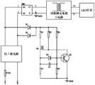
参考图2,LED调光系统中包含调光电源电路201和调光控制电路200。调光电源电路201包含调光器20,用于为LED灯提供功率,并根据调光器20调节LED灯的亮度。调光控制电路200连接于调光电源电路201,用于用于在调光器20的输出电压满足预设条件时为调光器20提供补偿电流。Referring to FIG. 2 , the LED dimming system includes a dimming
在本公开的一个实施例中,调光电源电路201包括:交流电源VAC,调光器20,桥式整流电路BD,照明控制电源。其中交流电源具有第一输出端与第二输出端;调光器20,耦接于交流电源VAC的第一输出端;桥式整流电路BD,负极耦接于调光器20的电压输出端,正极接地。照明控制电源,耦接于调光器20的电压输出端,且输出端连接于LED灯串。在本公开的示例性实施例中,照明控制电源包括直流-直流变换电路,但不限于此。In an embodiment of the present disclosure, the dimming
在本公开的一个实施例中,调光控制电路200包含整流模块21、输入电压检测模块22、处理器23以及恒流电路24,用于在调光器的输出电压满足预设条件时为调光器20提供补偿电流,以及在调光器20的输出电压不满足预设条件时停止提供补偿电流。在本公开的示例性实施例中,预设条件包括调光器输出电压的变化速度大于第一预设值或电压值小于第二预设值。In an embodiment of the present disclosure, the dimming
其中,整流电路21耦接于调光器20的电压输出端,用于对调光器20的输出电压进行整流并输出整流电压。The
输入电压检测电路22的输入端耦接于整流电路21,用于根据整流电压输出检测电压。The input terminal of the input
处理器23的输入端耦接于输入电压检测电路22的输出端,用于在检测电压满足预设条件时输出控制信号。The input end of the
恒流电路24的控制端耦接于处理器23的输出端,输出端耦接于整流电路21,用于响应控制信号输出或停止输出预设电流至整流电路21。The control end of the constant
其中,预设电流的电流值大于调光器的维持电流。Wherein, the current value of the preset current is greater than the maintaining current of the dimmer.
在本公开的示例性实施例中,调光器为前沿切向角调光器或后沿切向角调光器。In an exemplary embodiment of the present disclosure, the dimmer is a leading edge tangential angle dimmer or a trailing edge tangential angle dimmer.
本公开实施例提供的调光器控制电路通过在调光器的输出电压发生异常变化时为调光器提供大于其维持电流的补偿电流,有效避免了调光器从关闭到开启的过程中产生的震荡电流造成的调光器关闭,能够防止调光器开启过程中的光源闪烁。The dimmer control circuit provided by the embodiment of the present disclosure effectively avoids the occurrence of the dimmer during the process of turning off to on by providing the dimmer with a compensation current greater than its holding current when the output voltage of the dimmer changes abnormally. The dimmer is turned off due to the oscillating current, which can prevent the light source from flickering when the dimmer is turned on.
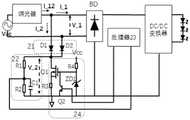
参考图3,在本公开的一个示例性实施例中,整流电路21可以包括:Referring to FIG. 3 , in an exemplary embodiment of the present disclosure, the
第一二极管D1,正极耦接于调光器电压输出端的第一端,负极耦接于第一节点N1。The anode of the first diode D1 is coupled to the first end of the voltage output terminal of the dimmer, and the cathode is coupled to the first node N1.
第二二极管D2,正极耦接于调光器电压输出端的第二端,负极耦接于第一节点N1。The anode of the second diode D2 is coupled to the second end of the voltage output terminal of the dimmer, and the cathode is coupled to the first node N1.
由D1和D2构成的整流电路对调光器20的输出电压V1进行整流,得到整流电压VN1。The rectifier circuit formed by D1 and D2 rectifies the output voltage V1 of the dimmer 20 to obtain the rectified voltage VN1 .
输入电压检测电路22可以包括:The input
第一电阻R1,一端耦接于第一节点N1,另一端耦接于输入电压检测电路22的输出端OUT。One end of the first resistor R1 is coupled to the first node N1 , and the other end is coupled to the output end OUT of the input
第二电阻R2,一端耦接于输入电压检测电路的输出端OUT,另一端接地。One end of the second resistor R2 is coupled to the output end OUT of the input voltage detection circuit, and the other end is grounded.
输入电压检测电路22通过设置R1和R2的比例,可以将整流电压VN1等比例变小,得到一个可以传递给处理器23的检测电压V2。其中,The input
V2=a*VN1 (1)V2=a*VN1 (1)
a为输入电压检测电路22的检测系数。a is the detection coefficient of the input
在一些实施例中,输入电压检测电路22还可以在输出端OUT和地之间配置滤波电容C1。In some embodiments, the input
图3所示的输入电压检测电路仅为一个实施例,本领域技术人员还可以根据本实施例的原理自行配置输入电压检测电路的元件与连接。The input voltage detection circuit shown in FIG. 3 is only an embodiment, and those skilled in the art can also configure the components and connections of the input voltage detection circuit by themselves according to the principles of this embodiment.
恒流电路24可以包括:The constant
第一开关元件Q1,具有第一端、第二端和控制端,第一端耦接于第一节点N1,第二端耦接于第二节点N2,控制端耦接于第三节点N3。The first switching element Q1 has a first terminal, a second terminal and a control terminal. The first terminal is coupled to the first node N1, the second terminal is coupled to the second node N2, and the control terminal is coupled to the third node N3.
第三电阻R3,一端耦接于第二节点N2,另一端接地。One end of the third resistor R3 is coupled to the second node N2, and the other end is grounded.
第二开关元件Q2,具有第一端、第二端和控制端,第一端耦接于第三节点N3,第二端接地,控制端耦接于处理器23的输出端CON。The second switching element Q2 has a first end, a second end and a control end, the first end is coupled to the third node N3 , the second end is grounded, and the control end is coupled to the output end CON of the
第四电阻R4,一端耦接于直流电压源VCC,另一端耦接于第三节点N3。The fourth resistor R4 has one end coupled to the DC voltage source VCC and the other end coupled to the third node N3.
稳压二极管ZD1,负极耦接于第三节点N3,正极接地。The Zener diode ZD1 has a cathode coupled to the third node N3 and an anode grounded.
稳定的直流电压源Vcc通过R4和ZD1产生一个稳定的电压Vg给Q1的栅极,使得Q1导通,流过R3的电流产生电压V_R3。当V_R3增大到大于Vg-Vth(Vth为Q1的导通阈值电压),Q1截止,R3的电流变小,V_R3减小,当V_R3小于Vg-Vth,Q1又导通,最后当V_R3等于Vg-Vth时,Q1工作在导通和截止的中间状态,使流经Q1的电流为恒定值,因此,恒流电路24可提供一恒定电流I,作为调光器的补偿电流,用于补偿调光器的电流。其中,恒定电流I满足以下公式:The stable DC voltage source Vcc generates a stable voltage Vg to the gate of Q1 through R4 and ZD1, so that Q1 is turned on, and the current flowing through R3 generates a voltage V_R3. When V_R3 increases to be greater than Vg-Vth (Vth is the turn-on threshold voltage of Q1), Q1 is turned off, the current of R3 becomes smaller, and V_R3 decreases. When V_R3 is less than Vg-Vth, Q1 is turned on again, and finally when V_R3 is equal to Vg At -Vth, Q1 works in the middle state of on and off, so that the current flowing through Q1 is a constant value. Therefore, the constant
I=(Vg-Vth)/R3 (2)I=(Vg-Vth)/R3 (2)
恒流电路24的开启和关闭可以由Q2控制。于Q2导通时,Vg变小,Q1截止,恒流电路24不输出恒流电流I;于Q2截止时,Vg增大,Q1导通,恒流电路24输出恒流电流I。The opening and closing of the constant
在图3所示的实施例中,处理器23的输入端IN耦接于输入电压检测电路22的输出端OUT,输出端CON耦接于第二开关元件Q2的控制端,用以根据输入电压检测电路22的输出电压V2控制第二开关元件Q2的开关,从而控制恒流电路24是否输出该恒流电流I。In the embodiment shown in FIG. 3 , the input terminal IN of the
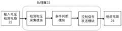
在本公开的示例性实施例中,如图4所示,处理器23可以包括:In an exemplary embodiment of the present disclosure, as shown in FIG. 4 , the
检测电压采集模块,用于按预设周期获取检测电压。The detection voltage acquisition module is used for acquiring the detection voltage according to a preset period.
条件判断模块,用于判断检测电压是否满足预设条件。The condition judgment module is used for judging whether the detection voltage satisfies the preset condition.
控制信号发送模块,用于在检测电压满足预设条件时发送第一控制信号,以及在检测电压不满足预设条件时发送第二控制信号,其中第一控制信号和第二控制信号分别用于控制第二开关元件Q2的关断和导通。a control signal sending module, configured to send a first control signal when the detected voltage meets a preset condition, and send a second control signal when the detected voltage does not meet the preset condition, wherein the first control signal and the second control signal are respectively used for The turn-off and turn-on of the second switching element Q2 are controlled.
其中,预设条件包括检测电压的变化速度大于第一预设值或电压值小于第二预设值。此时,恒流电路根据第一控制信号输出恒流电流I,根据第二控制信号停止输出恒流电流I。Wherein, the preset condition includes that the change speed of the detected voltage is greater than the first preset value or the voltage value is smaller than the second preset value. At this time, the constant current circuit outputs the constant current I according to the first control signal, and stops outputting the constant current I according to the second control signal.
处理器23例如可以为中央处理器、单片机或其他可编程控制器件,上述模块例如可以为逻辑模块或实体电路模块,只要能够实现所述功能即可,本公开对此不作特殊限定。The
本公开实施例的调光器可为前切调光器(前沿切向角调光器)或后切调光器(后沿切向角调光器)。下面将从这两种调光器的角度,分别通过图5~图9对处理器23的控制进行说明。The dimmer of the embodiment of the present disclosure may be a front-cut dimmer (leading edge tangential angle dimmer) or a rear-cut dimmer (trailing edge tangential angle dimmer). The following describes the control of the
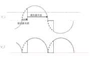
图5是本公开实施例应用到前切调光器(前沿切向角调光器)的原理示意图。FIG. 5 is a schematic diagram of the principle of applying an embodiment of the present disclosure to a front-cut dimmer (leading-edge tangential angle dimmer).
参考图5,Vac为输入侧的完整的交流工频电压源(可以理解为市电),V1为Vac经过前切调光器后的电源端输入电压,即,调光器的输出电压,检测电压V2是由调光器的输出电压V1经整流模块21整流以及输入电压检测模块22等比例缩小后得出的电压。Referring to Figure 5, Vac is the complete AC power frequency voltage source on the input side (which can be understood as commercial power), and V1 is the input voltage of the power supply terminal after Vac passes through the front-cut dimmer, that is, the output voltage of the dimmer. The voltage V2 is a voltage obtained after the output voltage V1 of the dimmer is rectified by the
当前切调光器关闭时,V1为0,当前切调光器开通时,V1为Vac。前切调光器通过调整开通和关闭的时间把调光信号传递给照明控制电源,照明控制电源根据该调光信号调整输出电流的大小从而实现调光。When the current-cut dimmer is turned off, V1 is 0, and when the current-cut dimmer is turned on, V1 is Vac. The front-cut dimmer transmits the dimming signal to the lighting control power supply by adjusting the turn-on and turn-off time, and the lighting control power supply adjusts the output current according to the dimming signal to realize dimming.
当前切调光器从关闭状态向导通状态时,电压的突然变化会导致产生较大的电压变化速度。由于照明控制电源存在输入电容,在开通瞬间会产生一个比较高的峰值电流,这个峰值电流存在震荡,震荡的最小值可能小于前切调光器导通所需的维持电流,从而造成前切调光器的关闭。为了在此时维持前切调光器的导通,本公开实施例在此时为维持电流外加一个补偿电流来维持前切调光器的导通。A sudden change in voltage can result in a large rate of voltage change when a front-cut dimmer goes from an off state to an on state. Due to the input capacitance of the lighting control power supply, a relatively high peak current will be generated at the moment of turn-on, and this peak current will oscillate. Turn off the light. In order to maintain the conduction of the front-cut dimmer at this time, the embodiment of the present disclosure adds a compensation current to the maintenance current at this time to maintain the conduction of the front-cut dimmer.
在本公开中,补偿电流由恒流电路24提供,处理器23控制恒流电路24的开启与关闭从而控制补偿电流的输出与停止输出。在一实施例中,处理器23通过判断检测电压V2的变化速度d(V2)/dt是否大于第一预设值Vref1来控制恒流电路24于预设时间tset内输出补偿电流。In the present disclosure, the compensation current is provided by the constant
第一预设值Vref1的取值例如可以为如图6所示,由调光器的输出电压V1的正弦波波形在30°角相切得到,如下公式(3):The value of the first preset value Vref1 may be, for example, as shown in FIG. 6 , obtained from the tangent of the sine wave waveform of the output voltage V1 of the dimmer at an angle of 30°, as shown in the following formula (3):
Vref1=V1_pk*tan30°*a (3)Vref1=V1_pk*tan30°*a (3)
其中,V1_pk为调光器的输出电压的峰值,a为输入电压检测电路22的检测系数。Wherein, V1_pk is the peak value of the output voltage of the dimmer, and a is the detection coefficient of the input
另外,在Vac较小时,流过前切调光器的电流也会变小,当这个电流小于前切调光器维持电流时,会导致前切调光器关闭。因此,在本公开的另一个实施例中,处理器23通过判断检测电压V2是否低于第二预设值Vref2来控制恒流电路24输出补偿电流。其中,第二预设值Vref2的取值可以包括但不限于:In addition, when Vac is small, the current flowing through the front-cut dimmer will also become smaller. When this current is less than the maintenance current of the front-cut dimmer, the front-cut dimmer will be turned off. Therefore, in another embodiment of the present disclosure, the
Vref2=Vmin*a (4)Vref2=Vmin*a (4)
其中,Vmin为最小的输入电压,可为V1_pk的1/4到1/2之间的任一电压值。Among them, Vmin is the minimum input voltage, which can be any voltage value between 1/4 and 1/2 of V1_pk.
如图7所示,对前切调光器输出电压V1而言,由关闭到导通瞬间,如时刻t1,电流I_1产生震荡,此时处理器23通过对检测电压V2进行判断,判断出dV2/dt大于第一预设值Vref1,由此于预设时间tset内输出Q2控制信号,以控制Q2关断,从而控制恒流电路24输出补偿电流I_2,其中I_2的值需大于或等于前切调光器维持电流。根据节点电流定律,流经前切调光器的电流I_12为I_1和I_2之和,由此,于导通瞬间t1,流经前切调光器的电流I_12必然大于前切调光器维持电流,使得前切调光器维持在导通状态。另外,如图7,当检测电压V2小于第二预设值Vref2时,如时刻t2,电流I_1足够低,难以维持前切调光器的导通,此时,控制Q2关断,控制恒流电路24输出补偿电流I_2,其中I_2的值需大于或等于前切调光器维持电流。由此,流经前切调光器的电流I_12必然大于前切调光器维持电流,使得前切调光器维持在导通状态。根据以上的实施例,于各种状态下,前切调光器均可维持在导通状态,使得前切调光器的导通和关断时间能正确地传递到照明控制电源上,有效避免了前切调光器开启后又关闭造成的光源闪烁。As shown in FIG. 7 , for the output voltage V1 of the front-cut dimmer, the current I_1 oscillates from the moment of turning off to turning on, such as time t1. At this time, the
图8是一种后切调光器(后沿切向角调光器)的工作原理示意图。FIG. 8 is a schematic diagram of the working principle of a back-cut dimmer (back-edge tangential angle dimmer).
参考图8,后切调光器一般用晶体管等开关元件控制相角的开启和关闭。由于后切调光器含有储能电容用以给控制器工作或者开关元件维持工作,当开关元件从导通到截止后,由于内部的电容导致电压V1不能有效地泄放到0,而高于相角关闭检测电压,导致所切的相角不能被有效地被检测出来,从而导致调光信号错误。Referring to FIG. 8 , the back-cut dimmer generally uses switching elements such as transistors to control the on and off of the phase angle. Since the post-cut dimmer contains energy storage capacitors for the controller to work or the switching elements to maintain operation, when the switching elements are turned from on to off, the voltage V1 cannot be effectively discharged to 0 due to the internal capacitance, and is higher than The phase angle turns off the detection voltage, so that the cut phase angle cannot be effectively detected, resulting in an error in the dimming signal.
图9是调光器控制电路应用在后切调光器上的原理示意图。FIG. 9 is a schematic diagram of the principle of applying a dimmer control circuit to a post-cut dimmer.
参考图9,在本公开一个实施例中,处理器23在判断检测电压V2小于第二预设值Vref2时,控制Q2从导通到截止,使恒流电路24产生一个预设值的恒定电流I_2,把存储在后切调光器中电容的电流泄放掉,使电压V1迅速降低到0,从而保证了切相角信号的准确检测。Referring to FIG. 9 , in an embodiment of the present disclosure, when the
图10是本公开实施例中一种调光器控制方法的流程图。FIG. 10 is a flowchart of a dimmer control method in an embodiment of the present disclosure.
参考图10,调光器维持电流控制方法可以包括:Referring to FIG. 10, the dimmer holding current control method may include:
步骤S91,按预设周期检测调光器输出电压。In step S91, the output voltage of the dimmer is detected according to a preset period.
步骤S92,在调光器输出电压满足预设条件时为调光器提供维持电流的补偿电流。Step S92, when the output voltage of the dimmer satisfies the preset condition, a compensation current for maintaining the current is provided for the dimmer.
步骤S93,在调光器输出电压不满足预设条件时停止提供补偿电流。Step S93, stop providing the compensation current when the output voltage of the dimmer does not meet the preset condition.
在本公开的示例性实施例中,预设条件包括调光器输出电压的变化速度大于第一预设值。In an exemplary embodiment of the present disclosure, the preset condition includes that the change speed of the output voltage of the dimmer is greater than the first preset value.
在本公开的另一个示例性实施例中,预设条件包括调光器输出电压的电压值小于第二预设值。In another exemplary embodiment of the present disclosure, the preset condition includes that the voltage value of the output voltage of the dimmer is smaller than the second preset value.
在本公开的示例性实施例中,补偿电流为恒定电流,恒定电流大于维持电流。In an exemplary embodiment of the present disclosure, the compensation current is a constant current that is greater than the sustaining current.
调光器控制方法900可以应用于调光器控制电路200的处理器23。The dimmer control method 900 may be applied to the
图11是调光器控制方法900的一个实施例。FIG. 11 is one embodiment of a dimmer control method 900 .
参考图11,在本公开一个实施例中,调光器控制方法示例性地可以包括:Referring to FIG. 11 , in one embodiment of the present disclosure, the dimmer control method may exemplarily include:
步骤S101,读取检测电压,记为V0;Step S101, read the detection voltage, denoted as V0;
步骤S102,间隔预设时间t再次读取检测电压,记为V1;Step S102, read the detection voltage again at an interval of a preset time t, denoted as V1;
步骤S103,计算电压变化速度K=(V1-V0)/t;Step S103, calculating the voltage change speed K=(V1-V0)/t;
步骤S104,判断K是否大于第一预设值,若是,进入步骤S105,若否,进入步骤S106;Step S104, determine whether K is greater than the first preset value, if yes, go to step S105, if not, go to step S106;
步骤S105,关闭Q2为预设时间tset,从而在预设时间内提供补偿电流至调光器,待预设时间tset结束后,开通Q2,并继续返回步骤S101读取检测电压,其中该补偿电流的电流值大于或等于调光器的维持电流;Step S105, turn off Q2 for the preset time tset, so as to provide the compensation current to the dimmer within the preset time, after the preset time tset ends, turn on Q2, and continue to return to step S101 to read the detection voltage, where the compensation current The current value is greater than or equal to the holding current of the dimmer;
步骤S106,判断当前检测电压V1是否小于第二预设值,若是,则进入步骤S107,关闭Q2,输出补偿电流至调光器,并继续返回步骤S101;若否,进入步骤S108,开启Q2,停止输出补偿电流,并继续返回步骤S101。Step S106, determine whether the current detection voltage V1 is less than the second preset value, if so, go to step S107, turn off Q2, output the compensation current to the dimmer, and continue to return to step S101; if not, go to step S108, turn on Q2, Stop outputting the compensation current, and continue to return to step S101.
需要说明的是,在本公开的其他实施例中,步骤S104和步骤S106的顺序还可以对调,只是,最终若K不大于第一预设值且V1不小于第二预设值,则均进入步骤S108,控制Q2开启,从而控制恒流电路24停止输出补偿电流。It should be noted that, in other embodiments of the present disclosure, the order of step S104 and step S106 can also be reversed, but in the end, if K is not greater than the first preset value and V1 is not less than the second preset value, both enter the In step S108, Q2 is controlled to be turned on, thereby controlling the constant
另外,上述从步骤S105、步骤S107或步骤S108返回到步骤S101继续读取检测电压的行为,也可以发生在读取V1后t时间(判断流程用时T<<t)。此时,读取的检测电压V2将与V1一起计算电压变化速度K,并判断V2是否大于第一预设值以及是否小于第二预设值。本领域技术人员可以自行设置检测顺序以及时间条件,本公开对此不作特殊限定。In addition, the above-mentioned behavior of returning from step S105, step S107 or step S108 to step S101 to continue reading the detection voltage may also occur at time t after V1 is read (time for the judgment process T<<t). At this time, the read detection voltage V2 will calculate the voltage change speed K together with V1, and determine whether V2 is greater than the first preset value and whether it is less than the second preset value. Those skilled in the art can set the detection sequence and time conditions by themselves, which are not specially limited in the present disclosure.
所属技术领域的技术人员能够理解,本发明的各个方面可以具体实现为以下形式,即:完全的硬件实施方式、完全的软件实施方式(包括固件、微代码等),或硬件和软件方面结合的实施方式,这里可以统称为“电路”、“模块”或“系统”。Those skilled in the art can understand that various aspects of the present invention can be embodied in the following forms, namely: a complete hardware implementation, a complete software implementation (including firmware, microcode, etc.), or a combination of hardware and software aspects. The implementations may be collectively referred to herein as "circuits," "modules," or "systems."
此外,上述附图仅是根据本发明示例性实施例的方法所包括的处理的示意性说明,而不是限制目的。易于理解,上述附图所示的处理并不表明或限制这些处理的时间顺序。另外,也易于理解,这些处理可以是例如在多个模块中同步或异步执行的。Furthermore, the above-mentioned figures are merely schematic illustrations of the processes included in the methods according to the exemplary embodiments of the present invention, and are not intended to be limiting. It is easy to understand that the processes shown in the above figures do not indicate or limit the chronological order of these processes. In addition, it is also readily understood that these processes may be performed synchronously or asynchronously in multiple modules, for example.
本领域技术人员在考虑说明书及实践这里公开的发明后,将容易想到本公开的其它实施方案。本申请旨在涵盖本公开的任何变型、用途或者适应性变化,这些变型、用途或者适应性变化遵循本公开的一般性原理并包括本公开未公开的本技术领域中的公知常识或惯用技术手段。说明书和实施例仅被视为示例性的,本公开的真正范围和构思由权利要求指出。Other embodiments of the present disclosure will readily occur to those skilled in the art upon consideration of the specification and practice of the invention disclosed herein. This application is intended to cover any variations, uses, or adaptations of the present disclosure that follow the general principles of the present disclosure and include common knowledge or techniques in the technical field not disclosed by the present disclosure . The specification and examples are to be regarded as exemplary only, with the true scope and spirit of the disclosure being indicated by the claims.
Claims (14)
Priority Applications (3)
| Application Number | Priority Date | Filing Date | Title |
|---|---|---|---|
| CN201810247972.9ACN110300476B (en) | 2018-03-23 | 2018-03-23 | Dimmer control circuit, method and system |
| JP2018221803AJP6764918B2 (en) | 2018-03-23 | 2018-11-28 | Dimmer control circuit, method and system |
| US16/354,285US10849195B2 (en) | 2018-03-23 | 2019-03-15 | Dimmer control circuit, method and system |
Applications Claiming Priority (1)
| Application Number | Priority Date | Filing Date | Title |
|---|---|---|---|
| CN201810247972.9ACN110300476B (en) | 2018-03-23 | 2018-03-23 | Dimmer control circuit, method and system |
Publications (2)
| Publication Number | Publication Date |
|---|---|
| CN110300476A CN110300476A (en) | 2019-10-01 |
| CN110300476Btrue CN110300476B (en) | 2022-04-12 |
Family
ID=67983878
Family Applications (1)
| Application Number | Title | Priority Date | Filing Date |
|---|---|---|---|
| CN201810247972.9AActiveCN110300476B (en) | 2018-03-23 | 2018-03-23 | Dimmer control circuit, method and system |
Country Status (3)
| Country | Link |
|---|---|
| US (1) | US10849195B2 (en) |
| JP (1) | JP6764918B2 (en) |
| CN (1) | CN110300476B (en) |
Families Citing this family (3)
| Publication number | Priority date | Publication date | Assignee | Title |
|---|---|---|---|---|
| JP7301710B2 (en)* | 2019-10-10 | 2023-07-03 | 大光電機株式会社 | Power supply and lighting equipment |
| CN111654939A (en)* | 2020-06-12 | 2020-09-11 | 厦门市必易微电子技术有限公司 | LED drive circuit, drive control circuit and drive control method |
| CN116419451A (en) | 2021-12-29 | 2023-07-11 | 台达电子企业管理(上海)有限公司 | Method for controlling bleeder connected to phase-cut dimmer and circuit connected to phase-cut dimmer |
Citations (5)
| Publication number | Priority date | Publication date | Assignee | Title |
|---|---|---|---|---|
| WO2004070675A2 (en)* | 2003-01-23 | 2004-08-19 | Gelcore Llc | Intelligent led traffic signals modules |
| CN104066229A (en)* | 2013-03-22 | 2014-09-24 | 东芝照明技术株式会社 | Power circuit and lighting device |
| CN104125680A (en)* | 2013-04-26 | 2014-10-29 | 东贝光电科技股份有限公司 | Variable power supply dimming control circuit |
| CN106937451A (en)* | 2017-04-28 | 2017-07-07 | 东莞泛美光电有限公司 | The LED drive circuit of compatible silicon controlled light modulator |
| CN107567130A (en)* | 2017-08-21 | 2018-01-09 | 矽力杰半导体技术(杭州)有限公司 | Power supply circuit and apply its LED drive circuit |
Family Cites Families (19)
| Publication number | Priority date | Publication date | Assignee | Title |
|---|---|---|---|---|
| US9155138B2 (en) | 2009-06-25 | 2015-10-06 | Koninklijke Philips N.V. | Driver for cooperating with a wall dimmer |
| ES2664198T3 (en)* | 2010-03-18 | 2018-04-18 | Philips Lighting Holding B.V. | Method and apparatus for increasing the dimming range of solid state lighting devices |
| JP2012085486A (en) | 2010-10-14 | 2012-04-26 | Steady Design Ltd | Dc power supply circuit |
| US9210744B2 (en) | 2012-04-18 | 2015-12-08 | Power Integrations, Inc. | Bleeder circuit for use in a power supply |
| CN104813743B (en)* | 2012-11-06 | 2017-08-18 | 飞利浦照明控股有限公司 | Circuit arrangement, LED lamp, lighting system and method of operation using the circuit arrangement |
| US9288864B2 (en) | 2012-12-10 | 2016-03-15 | Dialog Semiconductor Inc. | Adaptive holding current control for LED dimmer |
| US9408261B2 (en)* | 2013-05-07 | 2016-08-02 | Power Integrations, Inc. | Dimmer detector for bleeder circuit activation |
| TWI508615B (en) | 2013-06-04 | 2015-11-11 | Jin Fa Li | Active self-regulating circuit |
| US9148919B2 (en)* | 2013-12-06 | 2015-09-29 | Semiconductor Components Industries, Llc | Method for mitigating flicker |
| US9621062B2 (en) | 2014-03-07 | 2017-04-11 | Philips Lighting Holding B.V. | Dimmer output emulation with non-zero glue voltage |
| US9402293B2 (en)* | 2014-04-24 | 2016-07-26 | Power Integrations, Inc. | Multi-bleeder mode control for improved LED driver performance |
| CN203872419U (en)* | 2014-06-13 | 2014-10-08 | 成都芯源系统有限公司 | LED driving device and controller thereof |
| CN104020377A (en)* | 2014-06-13 | 2014-09-03 | 成都芯源系统有限公司 | LED driving device, controller thereof and dimming mode detection method |
| JP6399884B2 (en)* | 2014-10-10 | 2018-10-03 | シチズン時計株式会社 | LED drive circuit |
| US9484814B2 (en) | 2014-11-07 | 2016-11-01 | Power Integrations, Inc. | Power converter controller with analog controlled variable current circuit |
| US9572224B2 (en)* | 2014-11-07 | 2017-02-14 | Power Integrations, Inc. | Bleeder protection using thermal foldback |
| CN205249536U (en) | 2015-12-23 | 2016-05-18 | 珠海市圣昌电子有限公司 | A cut looks light modulator and maintain current control circuit for cutting power of adjusting luminance mutually |
| US9591710B1 (en)* | 2015-12-23 | 2017-03-07 | Zhuhai Shengchang Electronics Co., Ltd. | Kind of LED phase cut dimming power supply |
| JP6803560B2 (en)* | 2016-12-22 | 2020-12-23 | パナソニックIpマネジメント株式会社 | Lighting device and lighting equipment |
- 2018
- 2018-03-23CNCN201810247972.9Apatent/CN110300476B/enactiveActive
- 2018-11-28JPJP2018221803Apatent/JP6764918B2/enactiveActive
- 2019
- 2019-03-15USUS16/354,285patent/US10849195B2/enactiveActive
Patent Citations (5)
| Publication number | Priority date | Publication date | Assignee | Title |
|---|---|---|---|---|
| WO2004070675A2 (en)* | 2003-01-23 | 2004-08-19 | Gelcore Llc | Intelligent led traffic signals modules |
| CN104066229A (en)* | 2013-03-22 | 2014-09-24 | 东芝照明技术株式会社 | Power circuit and lighting device |
| CN104125680A (en)* | 2013-04-26 | 2014-10-29 | 东贝光电科技股份有限公司 | Variable power supply dimming control circuit |
| CN106937451A (en)* | 2017-04-28 | 2017-07-07 | 东莞泛美光电有限公司 | The LED drive circuit of compatible silicon controlled light modulator |
| CN107567130A (en)* | 2017-08-21 | 2018-01-09 | 矽力杰半导体技术(杭州)有限公司 | Power supply circuit and apply its LED drive circuit |
Also Published As
| Publication number | Publication date |
|---|---|
| JP2019169461A (en) | 2019-10-03 |
| US20190297715A1 (en) | 2019-09-26 |
| US10849195B2 (en) | 2020-11-24 |
| JP6764918B2 (en) | 2020-10-07 |
| CN110300476A (en) | 2019-10-01 |
Similar Documents
| Publication | Publication Date | Title |
|---|---|---|
| CN108200685B (en) | LED lighting system for thyristor switch control | |
| CN110113841B (en) | LED driving circuit with silicon controlled rectifier dimmer, circuit module and control method | |
| TWI738278B (en) | LED drive circuit and its operation method and power supply control module | |
| US8736185B2 (en) | SCR dimming circuit and method | |
| CN102869146B (en) | Self-selection holding current circuit | |
| CN103957634B (en) | Lighting system and control method thereof | |
| JP6617099B2 (en) | Stabilization circuit for low voltage lighting | |
| US20110115391A1 (en) | Led lamp and led lamp module | |
| CN107645804A (en) | System for LED switch control | |
| CN110300476B (en) | Dimmer control circuit, method and system | |
| CN103108470A (en) | Dynamic linear control light emitting diode (LED) driver circuit | |
| WO2017107146A1 (en) | Led drive circuit | |
| US20160270177A1 (en) | Lighting circuit, luminaire, and illumination system | |
| JP2016540481A (en) | Flyback fast start drive circuit and drive method | |
| JP5528883B2 (en) | LED drive circuit | |
| CN107736080A (en) | Light modulating device | |
| CN103889114B (en) | A kind of LED dimming driving circuit | |
| CN111239465B (en) | Line voltage detection circuit, system and method | |
| JP6481943B2 (en) | Light control device | |
| CN102883500A (en) | Dimmer | |
| TWI625032B (en) | Low phase surge protection device | |
| CN103904899A (en) | A switching power supply | |
| JP7029353B2 (en) | Power supply for lighting | |
| CN108029183A (en) | Light modulating device | |
| CN102281663A (en) | Light-emitting diode dimming control device with color temperature stabilizing function |
Legal Events
| Date | Code | Title | Description |
|---|---|---|---|
| PB01 | Publication | ||
| PB01 | Publication | ||
| SE01 | Entry into force of request for substantive examination | ||
| SE01 | Entry into force of request for substantive examination | ||
| GR01 | Patent grant | ||
| GR01 | Patent grant |