CN110275577B - Ultrasound module and display - Google Patents
Ultrasound module and displayDownload PDFInfo
- Publication number
- CN110275577B CN110275577BCN201910554542.6ACN201910554542ACN110275577BCN 110275577 BCN110275577 BCN 110275577BCN 201910554542 ACN201910554542 ACN 201910554542ACN 110275577 BCN110275577 BCN 110275577B
- Authority
- CN
- China
- Prior art keywords
- substrate
- sub
- piezoelectric material
- electrode
- material layer
- Prior art date
- Legal status (The legal status is an assumption and is not a legal conclusion. Google has not performed a legal analysis and makes no representation as to the accuracy of the status listed.)
- Expired - Fee Related
Links
Images


Classifications
- G—PHYSICS
- G06—COMPUTING OR CALCULATING; COUNTING
- G06F—ELECTRIC DIGITAL DATA PROCESSING
- G06F1/00—Details not covered by groups G06F3/00 - G06F13/00 and G06F21/00
- G06F1/16—Constructional details or arrangements
- G06F1/1613—Constructional details or arrangements for portable computers
- G06F1/1633—Constructional details or arrangements of portable computers not specific to the type of enclosures covered by groups G06F1/1615 - G06F1/1626
- G06F1/1637—Details related to the display arrangement, including those related to the mounting of the display in the housing
- G06F1/1643—Details related to the display arrangement, including those related to the mounting of the display in the housing the display being associated to a digitizer, e.g. laptops that can be used as penpads
- B—PERFORMING OPERATIONS; TRANSPORTING
- B06—GENERATING OR TRANSMITTING MECHANICAL VIBRATIONS IN GENERAL
- B06B—METHODS OR APPARATUS FOR GENERATING OR TRANSMITTING MECHANICAL VIBRATIONS OF INFRASONIC, SONIC, OR ULTRASONIC FREQUENCY, e.g. FOR PERFORMING MECHANICAL WORK IN GENERAL
- B06B1/00—Methods or apparatus for generating mechanical vibrations of infrasonic, sonic, or ultrasonic frequency
- B06B1/02—Methods or apparatus for generating mechanical vibrations of infrasonic, sonic, or ultrasonic frequency making use of electrical energy
- B06B1/06—Methods or apparatus for generating mechanical vibrations of infrasonic, sonic, or ultrasonic frequency making use of electrical energy operating with piezoelectric effect or with electrostriction
- B06B1/0688—Methods or apparatus for generating mechanical vibrations of infrasonic, sonic, or ultrasonic frequency making use of electrical energy operating with piezoelectric effect or with electrostriction with foil-type piezoelectric elements, e.g. PVDF
- B06B1/0692—Methods or apparatus for generating mechanical vibrations of infrasonic, sonic, or ultrasonic frequency making use of electrical energy operating with piezoelectric effect or with electrostriction with foil-type piezoelectric elements, e.g. PVDF with a continuous electrode on one side and a plurality of electrodes on the other side
- B—PERFORMING OPERATIONS; TRANSPORTING
- B06—GENERATING OR TRANSMITTING MECHANICAL VIBRATIONS IN GENERAL
- B06B—METHODS OR APPARATUS FOR GENERATING OR TRANSMITTING MECHANICAL VIBRATIONS OF INFRASONIC, SONIC, OR ULTRASONIC FREQUENCY, e.g. FOR PERFORMING MECHANICAL WORK IN GENERAL
- B06B1/00—Methods or apparatus for generating mechanical vibrations of infrasonic, sonic, or ultrasonic frequency
- B06B1/02—Methods or apparatus for generating mechanical vibrations of infrasonic, sonic, or ultrasonic frequency making use of electrical energy
- B06B1/0207—Driving circuits
- G—PHYSICS
- G06—COMPUTING OR CALCULATING; COUNTING
- G06V—IMAGE OR VIDEO RECOGNITION OR UNDERSTANDING
- G06V40/00—Recognition of biometric, human-related or animal-related patterns in image or video data
- G06V40/10—Human or animal bodies, e.g. vehicle occupants or pedestrians; Body parts, e.g. hands
- G06V40/12—Fingerprints or palmprints
- G06V40/13—Sensors therefor
- G06V40/1306—Sensors therefor non-optical, e.g. ultrasonic or capacitive sensing
- B—PERFORMING OPERATIONS; TRANSPORTING
- B06—GENERATING OR TRANSMITTING MECHANICAL VIBRATIONS IN GENERAL
- B06B—METHODS OR APPARATUS FOR GENERATING OR TRANSMITTING MECHANICAL VIBRATIONS OF INFRASONIC, SONIC, OR ULTRASONIC FREQUENCY, e.g. FOR PERFORMING MECHANICAL WORK IN GENERAL
- B06B2201/00—Indexing scheme associated with B06B1/0207 for details covered by B06B1/0207 but not provided for in any of its subgroups
- B06B2201/50—Application to a particular transducer type
- B06B2201/55—Piezoelectric transducer
- B06B2201/56—Foil type, e.g. PVDF
- B—PERFORMING OPERATIONS; TRANSPORTING
- B06—GENERATING OR TRANSMITTING MECHANICAL VIBRATIONS IN GENERAL
- B06B—METHODS OR APPARATUS FOR GENERATING OR TRANSMITTING MECHANICAL VIBRATIONS OF INFRASONIC, SONIC, OR ULTRASONIC FREQUENCY, e.g. FOR PERFORMING MECHANICAL WORK IN GENERAL
- B06B2201/00—Indexing scheme associated with B06B1/0207 for details covered by B06B1/0207 but not provided for in any of its subgroups
- B06B2201/70—Specific application
- G—PHYSICS
- G02—OPTICS
- G02F—OPTICAL DEVICES OR ARRANGEMENTS FOR THE CONTROL OF LIGHT BY MODIFICATION OF THE OPTICAL PROPERTIES OF THE MEDIA OF THE ELEMENTS INVOLVED THEREIN; NON-LINEAR OPTICS; FREQUENCY-CHANGING OF LIGHT; OPTICAL LOGIC ELEMENTS; OPTICAL ANALOGUE/DIGITAL CONVERTERS
- G02F1/00—Devices or arrangements for the control of the intensity, colour, phase, polarisation or direction of light arriving from an independent light source, e.g. switching, gating or modulating; Non-linear optics
- G02F1/01—Devices or arrangements for the control of the intensity, colour, phase, polarisation or direction of light arriving from an independent light source, e.g. switching, gating or modulating; Non-linear optics for the control of the intensity, phase, polarisation or colour
- G02F1/13—Devices or arrangements for the control of the intensity, colour, phase, polarisation or direction of light arriving from an independent light source, e.g. switching, gating or modulating; Non-linear optics for the control of the intensity, phase, polarisation or colour based on liquid crystals, e.g. single liquid crystal display cells
- G02F1/133—Constructional arrangements; Operation of liquid crystal cells; Circuit arrangements
- G02F1/1333—Constructional arrangements; Manufacturing methods
- G02F1/13338—Input devices, e.g. touch panels
- H—ELECTRICITY
- H10—SEMICONDUCTOR DEVICES; ELECTRIC SOLID-STATE DEVICES NOT OTHERWISE PROVIDED FOR
- H10K—ORGANIC ELECTRIC SOLID-STATE DEVICES
- H10K59/00—Integrated devices, or assemblies of multiple devices, comprising at least one organic light-emitting element covered by group H10K50/00
- H10K59/60—OLEDs integrated with inorganic light-sensitive elements, e.g. with inorganic solar cells or inorganic photodiodes
- H10K59/65—OLEDs integrated with inorganic image sensors
Landscapes
- Engineering & Computer Science (AREA)
- Theoretical Computer Science (AREA)
- Human Computer Interaction (AREA)
- Physics & Mathematics (AREA)
- General Physics & Mathematics (AREA)
- Mechanical Engineering (AREA)
- Multimedia (AREA)
- Computer Hardware Design (AREA)
- General Engineering & Computer Science (AREA)
- Transducers For Ultrasonic Waves (AREA)
- Image Input (AREA)
Abstract
Description
Translated fromChinese技术领域technical field
本发明属于显示技术领域,具体涉及一种超声模组及显示屏。The invention belongs to the technical field of display, and in particular relates to an ultrasonic module and a display screen.
背景技术Background technique
随着全面屏的显示器得到广泛关注,屏下指纹识别技术也得到越来越多人的重视。现有技术的一种屏下指纹识别技术采用超声指纹识别,具体的,如图1所示,超声模组包括第一电极11、第二电极12以及位于两电极之间的压电材料层13。其工作原理如下:第一电极11、第二电极12之间的电压不断变化,使得压电材料层13发生形变而产生机械振动,从而发出超声波;当手指或者其他事物靠近或者接触显示屏时,从手指或者其他事物反射回的超声波传到压电材料层13,使得压电材料层13产生电信号的变化,并将该电信号的变化反馈给其中一个电极,从而实现识别。As the full-screen display has received widespread attention, the under-screen fingerprint recognition technology has also received more and more attention. An under-screen fingerprint recognition technology in the prior art adopts ultrasonic fingerprint recognition. Specifically, as shown in FIG. 1 , the ultrasonic module includes a
然而,现技术的超声模组的超声波转化率低、超声波利用效率低,从而造成对手指或者其他事物的识别的性能较差的问题。However, the ultrasonic module of the prior art has low ultrasonic conversion rate and low ultrasonic utilization efficiency, thereby causing the problem of poor performance in recognizing fingers or other things.
发明内容SUMMARY OF THE INVENTION
本发明至少部分解决现有的超声模组的超声波转化率低的问题,提供一种超声波转化率高的超声模组。The present invention at least partially solves the problem of low ultrasonic conversion rate of the existing ultrasonic module, and provides an ultrasonic module with high ultrasonic conversion rate.
解决本发明技术问题所采用的技术方案是一种超声模组,包括:The technical solution adopted to solve the technical problem of the present invention is an ultrasonic module, including:
压电材料层;Piezoelectric material layer;
第一电极单元,设于所述压电材料层的一侧;a first electrode unit, arranged on one side of the piezoelectric material layer;
第二电极单元,设于所述压电材料层远离所述第一电极单元的一侧,所述第二电极单元包括多个相互间隔的第一子电极层和第一导电弹性材料,所述第一导电弹性材料位于所述第一子电极层和所述压电材料层之间的至少部分区域。The second electrode unit is disposed on the side of the piezoelectric material layer away from the first electrode unit, the second electrode unit includes a plurality of first sub-electrode layers and a first conductive elastic material spaced apart from each other, the The first conductive elastic material is located in at least a partial area between the first sub-electrode layer and the piezoelectric material layer.
进一步优选的是,所述第一导电弹性材料包括多个球形的接收电极导电弹性材料。Further preferably, the first conductive elastic material includes a plurality of spherical receiving electrode conductive elastic materials.
进一步优选的是,所述第二电极单元还包括多个第二子电极层,位于所述第一导电弹性材料和所述压电材料层之间;每个所述第一子电极层对应一个第二子电极层和一个球形的第一导电弹性材料。Further preferably, the second electrode unit further includes a plurality of second sub-electrode layers, located between the first conductive elastic material and the piezoelectric material layer; each of the first sub-electrode layers corresponds to one The second sub-electrode layer and a spherical first conductive elastic material.
进一步优选的是,所述第一电极单元包括至少一个第三子电极层和第二导电弹性材料,所述第二导电弹性材料位于所述第三子电极层和所述压电材料层之间。Further preferably, the first electrode unit includes at least one third sub-electrode layer and a second conductive elastic material, and the second conductive elastic material is located between the third sub-electrode layer and the piezoelectric material layer .
进一步优选的是,所述超声模组为超声指纹识别模组。Further preferably, the ultrasonic module is an ultrasonic fingerprint recognition module.
解决本发明技术问题所采用的技术方案是一种显示屏,包括:The technical solution adopted to solve the technical problem of the present invention is a display screen, including:
第一基板;a first substrate;
与所述第一基板对盒的第二基板;a second substrate assembled with the first substrate;
上述的超声模组,所述超声模组设于所述第一基板与第二基板之间,所述第一基板位于所述第一电极单元背离所述第二电极单元的一侧,所述第二基板位于所述第二电极单元背离所述第一电极单元的一侧。In the above ultrasonic module, the ultrasonic module is arranged between the first substrate and the second substrate, the first substrate is located on the side of the first electrode unit away from the second electrode unit, the The second substrate is located on a side of the second electrode unit away from the first electrode unit.
进一步优选的是,所述超声模组为上述的超声模组,所述显示屏还包括:支撑件,位于所述第二基板与所述压电材料层之间以及相邻所述球形的第一导电弹性材料之间,用于支撑所述第二基板与所述压电材料层。Further preferably, the ultrasonic module is the above-mentioned ultrasonic module, and the display screen further includes: a support member located between the second substrate and the piezoelectric material layer and adjacent to the spherical first part. between a conductive elastic material for supporting the second substrate and the piezoelectric material layer.
进一步优选的是,每个所述第一子电极层和与其对应第二子电极层对应所述显示屏的一个子像素。Further preferably, each of the first sub-electrode layer and the corresponding second sub-electrode layer corresponds to one sub-pixel of the display screen.
进一步优选的是,所述第二基板为具有驱动线路的驱动基板。Further preferably, the second substrate is a driving substrate having a driving circuit.
进一步优选的是,所述第一电极单元通过设于所述第一电极单元与所述第二基板之间的导电连接件与所述驱动基板电连接。Further preferably, the first electrode unit is electrically connected to the driving substrate through a conductive connection member provided between the first electrode unit and the second substrate.
附图说明Description of drawings
图1为现有的超声模组的结构示意图;Fig. 1 is the structural representation of the existing ultrasonic module;
图2为本发明的实施例的一种超声模组的结构示意图;2 is a schematic structural diagram of an ultrasonic module according to an embodiment of the present invention;
图3a至图3c为本发明的实施例的一种超声模组的工作原理的结构示意图;3a to 3c are schematic structural diagrams of the working principle of an ultrasonic module according to an embodiment of the present invention;
其中,附图标记为:10超声模组;11第一电极单元;12第二电极单元;121第一子电极层;122第二子电极层;123第一导电弹性材料;13压电材料层;21第一基板;22第二基板;30支撑件;40导电连接件。Wherein, the reference signs are: 10 ultrasonic module; 11 first electrode unit; 12 second electrode unit; 121 first sub-electrode layer; 122 second sub-electrode layer; 123 first conductive elastic material; 13 piezoelectric material layer ; 21 first substrate; 22 second substrate; 30 supports; 40 conductive connections.
具体实施方式Detailed ways
为使本领域技术人员更好地理解本发明的技术方案,下面结合附图和具体实施方式对本发明作进一步详细描述。In order to make those skilled in the art better understand the technical solutions of the present invention, the present invention will be further described in detail below with reference to the accompanying drawings and specific embodiments.
以下将参照附图更详细地描述本发明。在各个附图中,相同的元件采用类似的附图标记来表示。为了清楚起见,附图中的各个部分没有按比例绘制。此外,在图中可能未示出某些公知的部分。The present invention will be described in more detail below with reference to the accompanying drawings. In the various figures, like elements are designated by like reference numerals. For the sake of clarity, various parts in the figures have not been drawn to scale. Additionally, some well-known parts may not be shown in the drawings.
在下文中描述了本发明的许多特定的细节,例如部件的结构、材料、尺寸、处理工艺和技术,以便更清楚地理解本发明。但正如本领域的技术人员能够理解的那样,可以不按照这些特定的细节来实现本发明。Numerous specific details of the invention are described below, such as the construction of components, materials, dimensions, processing and techniques, in order to provide a clearer understanding of the invention. However, as can be understood by one skilled in the art, the present invention may be practiced without these specific details.
实施例1:Example 1:
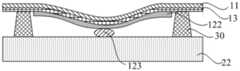
如图2、图3a、图3b以及图3c所示,本实施例提供一种超声模组10,包括:As shown in FIG. 2 , FIG. 3 a , FIG. 3 b and FIG. 3 c , this embodiment provides an
压电材料层13;
第一电极单元11,设于压电材料层13的一侧;The
第二电极单元12,设于压电材料层13远离第一电极单元11的一侧,第二电极单元12包括多个相互间隔的第一子电极层121和第一导电弹性材料123,第一导电弹性材料123位于第一子电极层121和压电材料层13之间的至少部分区域。The
其中,也就是说超声模组10的结构依次为第一电极单元11、压电材料层13、第一导电弹性材料123以及第一子电极层121。压电材料层13可以是聚偏氟乙烯(PVDF)膜层,也可以是氮化铝(AlN)、锆钛酸铅压电陶瓷(PZT)、氧化锌(ZnO)等其他无机或有机的材料层。Wherein, that is to say, the structure of the
该超声模组10的工作原理具体如下:对第一电极单元11和第二电极单元12施加电压而产生电场,压电材料层13处于该电场中,并且由于该电场的作用压电材料层13发生机械变形,从而产生超声波,并传播至第一电极单元11一侧(如手指或者其他外界事物的位置);当手指或者其他事物靠近该超声模组10的第一电极单元11时,压电材料层13发出的超声波由于手指或者其他外界事物而反射回压电材料层13中,使得压电材料层13再一次发生机械形变,此时的机械形变产生电信号,通过判断该电信号以识别上述信息。The working principle of the
需要说明的是,如图3a、图3b以及图3c所示,由于压电材料层13通过第一导电弹性材料123与第一子电极层121接触,故压电材料层13发生机械形变时第一导电弹性材料123可发生弹性变形,从而允许压电材料层13发生更大程度的形变。而在发射超声波时压电材料层13的形变越大在发射的超声波(即能量)也越多,同时在接收超声波时压电材料层13的形变越大产生可更多的电荷,使得电信号更准确;也就是说,压电材料层13的形变程度对于超声波的发射以及对反射回的超声波的识别具有重要的作用。It should be noted that, as shown in FIGS. 3 a , 3 b and 3 c , since the
本实施例的超声模组10中,在压电材料层13和第一子电极层121之间设置第一导电弹性材料123,由于第一导电弹性材料123是具有弹性的,因此与现有技术的超声模组10(没有设置导电弹性材料)相比,在足够大的电场中本实施例的超声模组10中的压电材料层13可发生更大程度的形变,即在发生超声波时能够产生更多的超声波,从而提高超声模组10发射率,在接收超声波时压电材料层13能够产生更准确的电信号,从而提高超声模组10识别性能。In the
优选的,第一导电弹性材料123包括多个球形的第一导电弹性材料123。Preferably, the first conductive
其中,也就是说第一导电弹性材料123并没有将压电材料层13和第一子电极层121之间的区域全部占满,即压电材料层13和第一子电极层121之间具有充满空气的间隙。That is to say, the first conductive
超声波由声阻抗大的材料传播至声阻抗小的材料时,会在两个材料的界面发生反射,这样压电材料层13发出的超声波会在压电材料层13和空气(空气的声阻抗小于压电材料层13的声阻抗)的界面处发生反射,从而可以提高从第一电极单元11传播出的超声波的量,同样从手指或者其他外界事物反射回的超声波也会在压电材料层13和空气的界面处发生反射,而再一次被压电材料层13吸收,提高压电材料层13的超声波吸收率,从而进一步的提高识别性能。When the ultrasonic wave propagates from a material with a large acoustic impedance to a material with a small acoustic impedance, it will be reflected at the interface of the two materials, so that the ultrasonic wave emitted by the
优选的,如图2所示,第二电极单元12还包括多个第二子电极层122,位于第一导电弹性材料123和压电材料层13之间;每个第一子电极层121对应一个第二子电极层122和一个球形的第一导电弹性材料123。Preferably, as shown in FIG. 2 , the
其中,相当于第二电极单元12分别为多个小组,每个小组中包括一个第一子电极层121、一个第二子电极层122和一个球形的第一导电弹性材料123,第一子电极层121和第二子电极层122在压电材料层13上的投影相同。Wherein, the
第二子电极层122的设置一方面可以增强第二电极单元12与压电材料层13之间的导电性,从而可以使得压电材料层13的机械形变转换电信号更加准确,另一方面可以加强第一电极单元11和第二电极单元12产生电场的能力,从而使得压电材料层13的机械形变更大、产生更多的超声波。On the one hand, the arrangement of the second
优选的,第一电极单元11包括至少一个第三子电极层和第二导电弹性材料,第二导电弹性材料位于第三子电极层和压电材料层13之间的至少部分区域。Preferably, the
其中,也就是说在第三子电极层和压电材料层13之间设置第二导电弹性材料。Therein, that is to say, the second conductive elastic material is provided between the third sub-electrode layer and the
这样在压电材料层13的两侧均设置弹性材料,在足够大的电场中,可进一步的增大压电材料层13的形变程度,即在发生超声波时能够产生更多的超声波,从而提高超声模组10发射率,在接收超声波时压电材料层13能够产生更准确的电信号,从而提高超声模组10识别性能。In this way, elastic materials are provided on both sides of the
具体的,第三子电极层的数量可为多个,且相互间隔。Specifically, the number of the third sub-electrode layers may be multiple and spaced from each other.
优选的,本实施例的超声模组10为超声指纹识别模组,即其发射的超声波可被指纹反射回来,且指纹的谷和脊的超声波反射率不同,从而通过分析各位置的超声波的强度,即可确定对应位置是谷还是脊,实现指纹识别。Preferably, the
此外,本实施例的超声模组10也可用于其他的需要发射超声和接收超声的设备或者场景中,例如触控、空间识别、手势识别等。In addition, the
实施例2:Example 2:
如图2、图3a、图3b以及图3c所示,本实施例提供一种显示屏,包括:As shown in FIG. 2 , FIG. 3 a , FIG. 3 b and FIG. 3 c , this embodiment provides a display screen, including:
第一基板21;the
与第一基板21对盒的第二基板22;a
实施例1中的超声模组10,超声模组10设于第一基板21与In the
第二基板22之间,第一基板21位于第一电极单元11背离第二电极单元12的一侧,第二基板22位于第二电极单元12背离第一电极单元11的一侧。Between the
其中,由于超声模组10的压电材料层13的至少一侧设置有导电弹性材料,即使超声模组10设于刚性的第一基板21与第二基板22之间,压电材料层13也能够发生较大的形变,因此,在发生超声波时能够产生更多的超声波,从而提高超声模组10发射率,在接收超声波时压电材料层13能够产生更准确的电信号,从而提高显示屏识别性能。Wherein, since at least one side of the
优选的,显示屏还包括:支撑件30,位于第二基板22与压电材料层13之间以及相邻球形的第一导电弹性材料123之间,用于支撑第二基板22与压电材料层13。Preferably, the display screen further includes: a
其中,也就是说在相邻的两个支撑件30之间具有一个第一子电极层121、一个第二子电极层122和一个球形的第一导电弹性材料123。支撑件30由非导电非弹性材料形成。支撑件30的横截面可以是环形或者方形,或者任意可实现的形状。此外,相邻的支撑件30与第二基板22、压电材料层13可形成独立封闭的腔室。Therein, that is to say, there is a first
支撑件30对压电材料层13和第二基板22的支撑不仅可保证第二电极单元12的结构稳固,而且保证第一导电弹性材料123的收缩性能,从而延长显示屏的寿命。The support of the
优选的,每个第一子电极层121和与其对应第二子电极层122对应显示屏的一个子像素。Preferably, each first
其中,也就是说每一组第一子电极层121、第二子电极层122和第一导电弹性材料123对应一个子像素,从而可以更准确的识别触控、指纹或者其他事物,以保证显示屏的识别性能更好。That is to say, each group of the first
具体的,第二基板22为具有驱动线路的驱动基板。第一基板21可为显示基板,例如,第一基板21包括由氧化铟锡(ITO)、钼(Mo)等材料形成的驱动电极(用于显示的电极)。Specifically, the
其中,第一电极单元11通过设于第一电极单元11与第二基板22之间的导电连接件40与驱动基板电连接。这样就不用单独设置给第一电极单元11提供电压的电路,使得该显示屏的结构简单。The
优选的,本实施的显示屏可以是触控显示屏,进一步是可实现指纹识别的触控显示屏。Preferably, the display screen of this embodiment may be a touch display screen, and further a touch display screen capable of realizing fingerprint recognition.
具体的,具有该显示屏的显示装置可为液晶显示面板、有机发光二极管(OLED)显示面板、电子纸、手机、平板电脑、电视机、显示器、笔记本电脑、数码相框、导航仪等任何具有显示功能的产品或部件。Specifically, the display device with the display screen can be any liquid crystal display panel, organic light emitting diode (OLED) display panel, electronic paper, mobile phone, tablet computer, TV, monitor, notebook computer, digital photo frame, navigator, etc. functional product or component.
其中,以上超声模组10可与用于显示的结构集成为一体,比如其中有的电极可同时作为显示用的电极,即第一基板21和第二基板22就是显示面板的两个基板。或者,以上超声模组10也可外挂于显示结构之外,例如其中的第二基板22也是显示面板的一个基板,而第一基板21则是设于显示面板外的。The above
应当说明的是,在本文中,诸如第一和第二等之类的关系术语仅仅用来将一个实体或者操作与另一个实体或操作区分开来,而不一定要求或者暗示这些实体或操作之间存在任何这种实际的关系或者顺序。而且,术语“包括”、“包含”或者其任何其他变体意在涵盖非排他性的包含,从而使得包括一系列要素的过程、方法、物品或者设备不仅包括那些要素,而且还包括没有明确列出的其他要素,或者是还包括为这种过程、方法、物品或者设备所固有的要素。在没有更多限制的情况下,由语句“包括一个……”限定的要素,并不排除在包括要素的过程、方法、物品或者设备中还存在另外的相同要素。It should be noted that, in this document, relational terms such as first and second are used only to distinguish one entity or operation from another entity or operation, and do not necessarily require or imply any relationship between these entities or operations. any such actual relationship or sequence exists. Moreover, the terms "comprising", "comprising" or any other variation thereof are intended to encompass a non-exclusive inclusion such that a process, method, article or device that includes a list of elements includes not only those elements, but also includes not explicitly listed or other elements inherent to such a process, method, article or apparatus. Without further limitation, an element qualified by the phrase "comprising a..." does not preclude the presence of additional identical elements in the process, method, article, or device that includes the element.
依照本发明的实施例如上文所述,这些实施例并没有详尽叙述所有的细节,也不限制该发明仅为所述的具体实施例。显然,根据以上描述,可作很多的修改和变化。本说明书选取并具体描述这些实施例,是为了更好地解释本发明的原理和实际应用,从而使所属技术领域技术人员能很好地利用本发明以及在本发明基础上的修改使用。本发明仅受权利要求书及其全部范围和等效物的限制。Embodiments in accordance with the present invention are described above, but these embodiments do not exhaust all the details and do not limit the invention to only the specific embodiments described. Obviously, many modifications and variations are possible in light of the above description. This specification selects and specifically describes these embodiments in order to better explain the principle and practical application of the present invention, so that those skilled in the art can make good use of the present invention and modifications based on the present invention. The present invention is to be limited only by the claims and their full scope and equivalents.
Claims (6)
Priority Applications (3)
| Application Number | Priority Date | Filing Date | Title |
|---|---|---|---|
| CN201910554542.6ACN110275577B (en) | 2019-06-25 | 2019-06-25 | Ultrasound module and display |
| US17/256,065US20210295003A1 (en) | 2019-06-25 | 2020-06-11 | Ultrasonic module, ultrasonic sensor and display screen |
| PCT/CN2020/095536WO2020259297A1 (en) | 2019-06-25 | 2020-06-11 | Ultrasonic module, ultrasonic sensor, and display screen |
Applications Claiming Priority (1)
| Application Number | Priority Date | Filing Date | Title |
|---|---|---|---|
| CN201910554542.6ACN110275577B (en) | 2019-06-25 | 2019-06-25 | Ultrasound module and display |
Publications (2)
| Publication Number | Publication Date |
|---|---|
| CN110275577A CN110275577A (en) | 2019-09-24 |
| CN110275577Btrue CN110275577B (en) | 2022-04-12 |
Family
ID=67962294
Family Applications (1)
| Application Number | Title | Priority Date | Filing Date |
|---|---|---|---|
| CN201910554542.6AExpired - Fee RelatedCN110275577B (en) | 2019-06-25 | 2019-06-25 | Ultrasound module and display |
Country Status (3)
| Country | Link |
|---|---|
| US (1) | US20210295003A1 (en) |
| CN (1) | CN110275577B (en) |
| WO (1) | WO2020259297A1 (en) |
Families Citing this family (6)
| Publication number | Priority date | Publication date | Assignee | Title |
|---|---|---|---|---|
| CN110275577B (en)* | 2019-06-25 | 2022-04-12 | 京东方科技集团股份有限公司 | Ultrasound module and display |
| CN112925431A (en)* | 2019-12-05 | 2021-06-08 | 北京小米移动软件有限公司 | Display panel and display device |
| CN111965877B (en)* | 2020-08-27 | 2023-09-22 | 京东方科技集团股份有限公司 | Color filter substrate and manufacturing method, display panel and manufacturing method, display equipment |
| CN114425156B (en)* | 2020-10-28 | 2025-05-13 | 北京小米移动软件有限公司 | Press sensing component and terminal device |
| CN113780184B (en)* | 2021-09-13 | 2024-11-08 | 上海天马微电子有限公司 | Ultrasonic fingerprint recognition module and display device |
| CN115971020B (en)* | 2023-01-17 | 2024-09-10 | 京东方科技集团股份有限公司 | Ultrasonic transducer, manufacturing method thereof and ultrasonic transduction system |
Citations (4)
| Publication number | Priority date | Publication date | Assignee | Title |
|---|---|---|---|---|
| CN1283779A (en)* | 1999-08-05 | 2001-02-14 | 松下电器产业株式会社 | Supersonic flowmeter of supersonic sensor |
| CN102522491A (en)* | 2011-12-14 | 2012-06-27 | 南京航空航天大学 | Polymer device with driving and sensing capability, preparation thereof and application thereof |
| CN207182314U (en)* | 2017-09-12 | 2018-04-03 | 南昌欧菲生物识别技术有限公司 | Display module and electronic device |
| JP2018056287A (en)* | 2016-09-28 | 2018-04-05 | 住友理工株式会社 | Transducer using flexible piezoelectric material |
Family Cites Families (7)
| Publication number | Priority date | Publication date | Assignee | Title |
|---|---|---|---|---|
| JP3985866B2 (en)* | 2001-12-05 | 2007-10-03 | 富士フイルム株式会社 | Ultrasonic transducer and manufacturing method thereof |
| CN101390174A (en)* | 2006-02-27 | 2009-03-18 | 日立化成工业株式会社 | Circuit connecting material, connection structure for circuit member using the same, and method for producing such connection structure |
| JP4650456B2 (en)* | 2006-08-25 | 2011-03-16 | 日立化成工業株式会社 | Circuit connection material, circuit member connection structure using the same, and manufacturing method thereof |
| US20120073388A1 (en)* | 2009-05-22 | 2012-03-29 | University Of New Brunswick | Force sensing compositions, devices and methods |
| CN106855764B (en)* | 2015-12-09 | 2023-05-02 | 安徽精卓光显技术有限责任公司 | Touch display device |
| CN107832665A (en)* | 2017-10-10 | 2018-03-23 | 成都安瑞芯科技有限公司 | Display module and electronic equipment |
| CN110275577B (en)* | 2019-06-25 | 2022-04-12 | 京东方科技集团股份有限公司 | Ultrasound module and display |
- 2019
- 2019-06-25CNCN201910554542.6Apatent/CN110275577B/ennot_activeExpired - Fee Related
- 2020
- 2020-06-11WOPCT/CN2020/095536patent/WO2020259297A1/ennot_activeCeased
- 2020-06-11USUS17/256,065patent/US20210295003A1/ennot_activeAbandoned
Patent Citations (4)
| Publication number | Priority date | Publication date | Assignee | Title |
|---|---|---|---|---|
| CN1283779A (en)* | 1999-08-05 | 2001-02-14 | 松下电器产业株式会社 | Supersonic flowmeter of supersonic sensor |
| CN102522491A (en)* | 2011-12-14 | 2012-06-27 | 南京航空航天大学 | Polymer device with driving and sensing capability, preparation thereof and application thereof |
| JP2018056287A (en)* | 2016-09-28 | 2018-04-05 | 住友理工株式会社 | Transducer using flexible piezoelectric material |
| CN207182314U (en)* | 2017-09-12 | 2018-04-03 | 南昌欧菲生物识别技术有限公司 | Display module and electronic device |
Also Published As
| Publication number | Publication date |
|---|---|
| US20210295003A1 (en) | 2021-09-23 |
| CN110275577A (en) | 2019-09-24 |
| WO2020259297A1 (en) | 2020-12-30 |
Similar Documents
| Publication | Publication Date | Title |
|---|---|---|
| CN110275577B (en) | Ultrasound module and display | |
| CN111758099B (en) | Fingerprint identification module, driving method and manufacturing method thereof and display device | |
| US20220230009A1 (en) | Fingerprint recognition module, display panel and driving method, and display device | |
| CN110097043B (en) | Sensor pixels, ultrasonic sensors, OLED display panels, and OLED display devices | |
| US20210303814A1 (en) | Fingerprint identification device and driving method thereof, display device | |
| CN205983304U (en) | Display device and user terminal | |
| CN109815918A (en) | Fingerprint identification module and its manufacturing method and driving method, and display device | |
| CN111695388B (en) | Fingerprint recognition structure and driving method thereof, and display device | |
| CN107451572B (en) | Ultrasonic fingerprint recognition module and electronic equipment | |
| CN111782090B (en) | Display module, ultrasonic touch detection method and ultrasonic fingerprint identification method | |
| CN110472606B (en) | An ultrasonic identification module, its driving method and display device | |
| CN107958199B (en) | Fingerprint detection module, display device and electronic equipment | |
| KR102795248B1 (en) | Display device including ultrasonic detection device | |
| CN205691915U (en) | A kind of display floater and display device | |
| CN207182329U (en) | Electronic equipment | |
| CN110175586A (en) | A kind of fingerprint recognition mould group and its fingerprint identification method, display device | |
| TW202305573A (en) | Ultrasonic fingerprint recognition assembly, electronic device, and ultrasonic fingerprint recognition method | |
| CN110287901A (en) | Ultrasonic sensors and electronics | |
| CN107832671A (en) | Display device and electronic equipment | |
| CN112181208B (en) | Touch control identification device, display device and manufacturing method thereof | |
| WO2025007824A1 (en) | Ultrasonic fingerprint recognition module, system, and electronic device | |
| CN112753062B (en) | Fingerprint identification circuit and its driving method, fingerprint identification module and display device | |
| CN207182322U (en) | Ultrasonic sensors and electronics | |
| CN114120878B (en) | A display panel, a driving method thereof and a display device | |
| CN207557966U (en) | Display module and electronic device |
Legal Events
| Date | Code | Title | Description |
|---|---|---|---|
| PB01 | Publication | ||
| PB01 | Publication | ||
| SE01 | Entry into force of request for substantive examination | ||
| SE01 | Entry into force of request for substantive examination | ||
| GR01 | Patent grant | ||
| GR01 | Patent grant | ||
| CF01 | Termination of patent right due to non-payment of annual fee | Granted publication date:20220412 | |
| CF01 | Termination of patent right due to non-payment of annual fee |