CN110273322B - Nano paper, preparation method, method for carrying out graphic processing and electronic equipment - Google Patents
Nano paper, preparation method, method for carrying out graphic processing and electronic equipmentDownload PDFInfo
- Publication number
- CN110273322B CN110273322BCN201910537795.2ACN201910537795ACN110273322BCN 110273322 BCN110273322 BCN 110273322BCN 201910537795 ACN201910537795 ACN 201910537795ACN 110273322 BCN110273322 BCN 110273322B
- Authority
- CN
- China
- Prior art keywords
- nanopaper
- pressure sensing
- graphic
- signal
- transparent substrate
- Prior art date
- Legal status (The legal status is an assumption and is not a legal conclusion. Google has not performed a legal analysis and makes no representation as to the accuracy of the status listed.)
- Active
Links
Images


Classifications
- D—TEXTILES; PAPER
- D21—PAPER-MAKING; PRODUCTION OF CELLULOSE
- D21H—PULP COMPOSITIONS; PREPARATION THEREOF NOT COVERED BY SUBCLASSES D21C OR D21D; IMPREGNATING OR COATING OF PAPER; TREATMENT OF FINISHED PAPER NOT COVERED BY CLASS B31 OR SUBCLASS D21G; PAPER NOT OTHERWISE PROVIDED FOR
- D21H11/00—Pulp or paper, comprising cellulose or lignocellulose fibres of natural origin only
- D21H11/16—Pulp or paper, comprising cellulose or lignocellulose fibres of natural origin only modified by a particular after-treatment
- D21H11/18—Highly hydrated, swollen or fibrillatable fibres
- G—PHYSICS
- G06—COMPUTING OR CALCULATING; COUNTING
- G06F—ELECTRIC DIGITAL DATA PROCESSING
- G06F3/00—Input arrangements for transferring data to be processed into a form capable of being handled by the computer; Output arrangements for transferring data from processing unit to output unit, e.g. interface arrangements
- G06F3/01—Input arrangements or combined input and output arrangements for interaction between user and computer
- G06F3/03—Arrangements for converting the position or the displacement of a member into a coded form
- G06F3/041—Digitisers, e.g. for touch screens or touch pads, characterised by the transducing means
- G06F3/0414—Digitisers, e.g. for touch screens or touch pads, characterised by the transducing means using force sensing means to determine a position
- G06F3/04142—Digitisers, e.g. for touch screens or touch pads, characterised by the transducing means using force sensing means to determine a position the force sensing means being located peripherally, e.g. disposed at the corners or at the side of a touch sensing plate
- G—PHYSICS
- G06—COMPUTING OR CALCULATING; COUNTING
- G06F—ELECTRIC DIGITAL DATA PROCESSING
- G06F3/00—Input arrangements for transferring data to be processed into a form capable of being handled by the computer; Output arrangements for transferring data from processing unit to output unit, e.g. interface arrangements
- G06F3/01—Input arrangements or combined input and output arrangements for interaction between user and computer
- G06F3/03—Arrangements for converting the position or the displacement of a member into a coded form
- G06F3/041—Digitisers, e.g. for touch screens or touch pads, characterised by the transducing means
- G06F3/0414—Digitisers, e.g. for touch screens or touch pads, characterised by the transducing means using force sensing means to determine a position
- G06F3/04144—Digitisers, e.g. for touch screens or touch pads, characterised by the transducing means using force sensing means to determine a position using an array of force sensing means
- D—TEXTILES; PAPER
- D21—PAPER-MAKING; PRODUCTION OF CELLULOSE
- D21H—PULP COMPOSITIONS; PREPARATION THEREOF NOT COVERED BY SUBCLASSES D21C OR D21D; IMPREGNATING OR COATING OF PAPER; TREATMENT OF FINISHED PAPER NOT COVERED BY CLASS B31 OR SUBCLASS D21G; PAPER NOT OTHERWISE PROVIDED FOR
- D21H27/00—Special paper not otherwise provided for, e.g. made by multi-step processes
- G—PHYSICS
- G01—MEASURING; TESTING
- G01L—MEASURING FORCE, STRESS, TORQUE, WORK, MECHANICAL POWER, MECHANICAL EFFICIENCY, OR FLUID PRESSURE
- G01L1/00—Measuring force or stress, in general
- G01L1/20—Measuring force or stress, in general by measuring variations in ohmic resistance of solid materials or of electrically-conductive fluids; by making use of electrokinetic cells, i.e. liquid-containing cells wherein an electrical potential is produced or varied upon the application of stress
- G01L1/205—Measuring force or stress, in general by measuring variations in ohmic resistance of solid materials or of electrically-conductive fluids; by making use of electrokinetic cells, i.e. liquid-containing cells wherein an electrical potential is produced or varied upon the application of stress using distributed sensing elements
- G—PHYSICS
- G06—COMPUTING OR CALCULATING; COUNTING
- G06F—ELECTRIC DIGITAL DATA PROCESSING
- G06F3/00—Input arrangements for transferring data to be processed into a form capable of being handled by the computer; Output arrangements for transferring data from processing unit to output unit, e.g. interface arrangements
- G06F3/01—Input arrangements or combined input and output arrangements for interaction between user and computer
- G06F3/03—Arrangements for converting the position or the displacement of a member into a coded form
- G06F3/041—Digitisers, e.g. for touch screens or touch pads, characterised by the transducing means
- G06F3/0414—Digitisers, e.g. for touch screens or touch pads, characterised by the transducing means using force sensing means to determine a position
- G—PHYSICS
- G06—COMPUTING OR CALCULATING; COUNTING
- G06F—ELECTRIC DIGITAL DATA PROCESSING
- G06F3/00—Input arrangements for transferring data to be processed into a form capable of being handled by the computer; Output arrangements for transferring data from processing unit to output unit, e.g. interface arrangements
- G06F3/01—Input arrangements or combined input and output arrangements for interaction between user and computer
- G06F3/03—Arrangements for converting the position or the displacement of a member into a coded form
- G06F3/041—Digitisers, e.g. for touch screens or touch pads, characterised by the transducing means
- G06F3/045—Digitisers, e.g. for touch screens or touch pads, characterised by the transducing means using resistive elements, e.g. a single continuous surface or two parallel surfaces put in contact
- G—PHYSICS
- G06—COMPUTING OR CALCULATING; COUNTING
- G06F—ELECTRIC DIGITAL DATA PROCESSING
- G06F2203/00—Indexing scheme relating to G06F3/00 - G06F3/048
- G06F2203/041—Indexing scheme relating to G06F3/041 - G06F3/045
- G06F2203/04102—Flexible digitiser, i.e. constructional details for allowing the whole digitising part of a device to be flexed or rolled like a sheet of paper
Landscapes
- Engineering & Computer Science (AREA)
- General Engineering & Computer Science (AREA)
- Theoretical Computer Science (AREA)
- Physics & Mathematics (AREA)
- General Physics & Mathematics (AREA)
- Human Computer Interaction (AREA)
- Force Measurement Appropriate To Specific Purposes (AREA)
- Devices For Indicating Variable Information By Combining Individual Elements (AREA)
- Position Input By Displaying (AREA)
Abstract
Description
Translated fromChinese技术领域technical field
本发明涉及显示领域,具体地,涉及纳米纸及制备方法、进行图形处理的方法以及电子设备。The present invention relates to the field of display, in particular, to nanopaper and a preparation method, a method for performing graphic processing, and an electronic device.
背景技术Background technique
目前的手写电子输入设备,已经可实现通过特殊的笔在普通纸上进行输入,并将书写内容同步保存于电子设备中。即可以用数位笔在任何纸面上记录手写内容,并将手写内容将转化为数字文件,存储在常用的电子设备,例如手机或平板中。但是目前基于智能可书写工具对电子设备中存储的原稿进行修改,如修改线条、删除内容等操作仍旧比较困难,且手写电子输入设备配置的笔并不适合在普通电子设备的屏幕上进行操作。The current handwriting electronic input device can realize input on ordinary paper through a special pen, and synchronously save the writing content in the electronic device. That is, handwriting can be recorded on any paper with a digital pen, and the handwriting will be converted into a digital file and stored in a commonly used electronic device, such as a mobile phone or tablet. However, it is still difficult to modify manuscripts stored in electronic devices based on intelligent writing tools, such as modifying lines and deleting content, and the pen configured on handwriting electronic input devices is not suitable for operation on the screen of ordinary electronic devices.
因此,目前的纳米纸及制备方法、进行图形处理的方法以及电子设备仍有待提高。Therefore, the current nanopaper and its preparation method, the method for performing graphic processing and the electronic equipment still need to be improved.
发明内容SUMMARY OF THE INVENTION
有鉴于此,本发明的一个目的在于提出一种可灵活进行操作的纳米纸。具体地,该纳米纸包括:透明衬底,所述透明衬底包括微纳纤维;多个压力传感单元,所述压力传感单元位于所述透明衬底的一侧,且所述压力传感单元的电阻可随着所述透明衬底发生形变而改变;多个导线,多个所述导线与所述压力传感单元相连,且被配置为可单独输出多个所述压力传感单元中的每一个的传感信号。由此,该纳米纸可以对作用于其表面的压力进行传感,且采用透明衬底可提高该纳米纸的整体透过率,可以将该纳米纸置于电子设备的显示屏上方,结合显示屏显示的图形进行操作。In view of this, an object of the present invention is to propose a nanopaper that can be operated flexibly. Specifically, the nanopaper includes: a transparent substrate including micro-nano fibers; a plurality of pressure sensing units, the pressure sensing units are located on one side of the transparent substrate, and the pressure transmitter The resistance of the sensing unit can be changed as the transparent substrate is deformed; a plurality of wires are connected to the pressure sensing unit, and are configured to independently output a plurality of the pressure sensing units sensing signal of each. Therefore, the nanopaper can sense the pressure acting on its surface, and the use of a transparent substrate can improve the overall transmittance of the nanopaper. operate according to the graphics displayed on the screen.
根据本发明的实施例,压力传感单元具有压力传感层,所述压力传感层是由层状纳米材料形成的。由此,可以提高该压力传感单元的压力传感效果。According to an embodiment of the present invention, the pressure sensing unit has a pressure sensing layer formed of a layered nanomaterial. Thereby, the pressure sensing effect of the pressure sensing unit can be improved.
根据本发明的实施例,所述层状纳米材料包括石墨烯、MoS2,WS2,MoSe2以及WSe2的至少之一。由此,可以进一步提高该压力传感单元的压力传感效果。According to an embodiment of the present invention, the layered nanomaterial includes at least one of graphene, MoS2 , WS2 , MoSe2 and WSe2 . Thereby, the pressure sensing effect of the pressure sensing unit can be further improved.
根据本发明的实施例,多个所述压力传感单元在所述透明衬底上阵列排布,所述纳米纸进一步包括:多个第一连接端口,每个所述第一连接端口通过所述导线与位于同一行的多个所述压力传感单元均相连,或者每个所述第一端口与位于同一列的多个所述压力传感单元均相连,以及多个第二连接端口,所述第二连接端口通过所述导线与所述压力传感单元一一对应连接。由此,可简便地单独输出每个压力传感单元的传感信号,从而进一步提高该压力传感单元的灵敏度。According to an embodiment of the present invention, a plurality of the pressure sensing units are arranged in an array on the transparent substrate, and the nanopaper further includes: a plurality of first connection ports, each of the first connection ports passing through the transparent substrate. The wires are connected to a plurality of the pressure sensing units located in the same row, or each of the first ports is connected to a plurality of the pressure sensing units located in the same column, and a plurality of second connection ports, The second connection port is connected with the pressure sensing unit in a one-to-one correspondence through the wire. Thereby, the sensing signal of each pressure sensing unit can be simply outputted individually, thereby further improving the sensitivity of the pressure sensing unit.
根据本发明的实施例,所述纳米纸的透过率高于90%。由此,该纳米纸具有较高的透过率,可通过将该纳米纸置于显示屏上方,结合显示屏显示的画面进行书写。According to an embodiment of the present invention, the transmittance of the nanopaper is higher than 90%. Therefore, the nanopaper has high transmittance, and writing can be performed by placing the nanopaper above the display screen and combining with the picture displayed by the display screen.
根据本发明的实施例,所述纳米纸进一步包括以下结构的至少之一:电源模块,所述电源模块与所述压力传感单元电连接;蓝牙传输模块,所述蓝牙传输模块被配置为可接收多个所述压力传感单元中的每一个的传感信号;固定胶层,所述固定胶层位于所述透明衬底未设置所述压力传感单元的一侧,所述固定胶层在所述透明衬底上的投影位于所述透明衬底的边缘处,且所述固定胶层远离所述透明衬底一侧的表面具有粘性。由此,可进一步提高该纳米纸的性能。According to an embodiment of the present invention, the nanopaper further comprises at least one of the following structures: a power module, which is electrically connected with the pressure sensing unit; a Bluetooth transmission module, which is configured to be capable of receiving a sensing signal from each of the plurality of pressure sensing units; fixing the adhesive layer, the fixing adhesive layer is located on the side of the transparent substrate where the pressure sensing unit is not arranged, the fixing adhesive layer The projection on the transparent substrate is located at the edge of the transparent substrate, and the surface of the fixing adhesive layer on the side away from the transparent substrate has stickiness. Thus, the performance of the nanopaper can be further improved.
在本发明的又一方面,本发明提出了一种利用前面所述的纳米纸进行图形处理的方法。该方法包括:将所述纳米纸置于电子设备的显示屏上,并利用所述纳米纸的所述压力传感单元,记录对所述纳米纸表面进行的图形处理信号,所述图形处理信号包括压力运动轨迹信号以及按压压力信号的至少之一;将所述图形处理信号发送至所述电子设备,以便所述电子设备基于所述图形处理信号进行图形处理。该方法可以利用结构简单的纳米纸进行图形处理,且可利用纳米纸进行压力传感,从而记录书写的轨迹以及笔记的压力。由此,可通过简单的触控,实现对电子设备中的图形进行处理。In yet another aspect of the present invention, the present invention provides a method for pattern processing using the aforementioned nanopaper. The method includes: placing the nanopaper on a display screen of an electronic device, and using the pressure sensing unit of the nanopaper to record a graphic processing signal performed on the surface of the nanopaper, the graphic processing signal Including at least one of a pressure movement track signal and a pressing pressure signal; and sending the graphics processing signal to the electronic device, so that the electronic device performs graphics processing based on the graphics processing signal. The method can use nanopaper with a simple structure for graphic processing, and can use nanopaper for pressure sensing, so as to record the trajectory of writing and the pressure of notes. Therefore, the graphics in the electronic device can be processed through a simple touch.
根据本发明的实施例,基于所述图形处理信号进行图形处理进一步包括:在所述第一处理模式下,所述电子设备基于所述图形处理信号在需要进行处理的图形中增加图形内容。由此,可以简便的对原有图形进行增加内容的处理。According to an embodiment of the present invention, performing graphics processing based on the graphics processing signal further includes: in the first processing mode, the electronic device adds graphics content to graphics to be processed based on the graphics processing signal. In this way, the process of adding content to the original graphics can be easily performed.
根据本发明的实施例,所述增加图形内容包括:基于所述图形处理信号中的压力运动轨迹信号以及按压压力信号,确定增加的图形的位置、形状或颜色的深浅。由此,可进一步提高图形处理的效果。According to an embodiment of the present invention, the adding graphic content includes: determining the position, shape or color depth of the added graphic based on the pressure movement track signal and the pressing pressure signal in the graphic processing signal. Thereby, the effect of the graphics processing can be further improved.
根据本发明的实施例,基于所述图形处理信号进行图形处理进一步包括:在所述第二处理模式下,所述电子设备基于所述图形处理信号对需要进行处理的图形进行擦除处理。由此,可进一步提高图形处理的效果。According to an embodiment of the present invention, performing graphics processing based on the graphics processing signal further includes: in the second processing mode, the electronic device performs erasing processing on graphics to be processed based on the graphics processing signal. Thereby, the effect of the graphics processing can be further improved.
根据本发明的实施例,所述擦除处理包括:基于所述图形处理信号中的所述压力运动轨迹信号确定擦除区域,并基于所述按压压力信号,调节所述图形在所述擦除区域的透明度。由此,可进一步提高图形处理的效果。According to an embodiment of the present invention, the erasing process includes: determining an erasing area based on the pressure movement track signal in the graphics processing signal, and adjusting the erasing area of the graphics based on the pressing pressure signal Transparency of the area. Thereby, the effect of the graphics processing can be further improved.
根据本发明的实施例,所述纳米纸的面积小于所述电子设备的显示屏的面积,所述显示屏为触控显示屏,所述方法进一步包括:将所述纳米纸固定在所述触控显示屏中需要进行图形处理的位置,并在所述纳米纸记录所述图形处理信号之前,预先对进行所述图形处理的区域进行校正。由此,可进一步提高图形处理的效果。According to an embodiment of the present invention, the area of the nanopaper is smaller than that of the display screen of the electronic device, and the display screen is a touch display screen, and the method further includes: fixing the nanopaper on the touch screen. The position in the display screen where graphics processing needs to be performed is controlled, and before the nanopaper records the graphic processing signal, the area where the graphic processing is performed is corrected in advance. Thereby, the effect of the graphics processing can be further improved.
根据本发明的实施例,所述电子设备基于所述图形处理信号进行图形处理包括:将所述图形处理信号与所述电子设备中存储的标准信号进行比对,并基于比对结果,生成临摹图形,所述临摹图形为基于所述标准信号形成的图形,和基于所述图形处理信号形成的图形的叠加图形。由此,可进一步提高图形处理的效果。According to an embodiment of the present invention, the electronic device performing graphics processing based on the graphics processing signal includes: comparing the graphics processing signal with a standard signal stored in the electronic device, and generating a copy based on the comparison result A graphic, the copied graphic is a graphic formed based on the standard signal and a superimposed graphic of a graphic formed based on the graphic processing signal. Thereby, the effect of the graphics processing can be further improved.
在本发明的另一方面,本发明提出了一种制备纳米纸的方法。该方法包括:提供透明衬底;在所述透明衬底上形成多个压力传感单元以及多个导线,令所述压力传感单元的电阻可随着所述透明衬底发生形变而改变,并可通过所述导线单独输出多个所述压力传感单元中的每一个的传感信号。由此,可简便地获得结构简便的纳米纸。In another aspect of the present invention, the present invention provides a method for preparing nanopaper. The method includes: providing a transparent substrate; forming a plurality of pressure sensing units and a plurality of wires on the transparent substrate, so that the resistance of the pressure sensing units can be changed with the deformation of the transparent substrate, The sensing signal of each of the plurality of pressure sensing units can be individually output through the wire. Thereby, nanopaper with a simple structure can be easily obtained.
在本发明的又一方面,本发明提出了一种电子设备。该电子设备包括:显示屏以及主板,所述主板与所述显示屏电连接;前面所述的纳米纸,所述纳米纸可揭除地位于所述显示屏上,所述纳米纸被配置为可向所述主板输出多个压力传感单元的传感信号。由此,该电子设备具有前述的纳米纸所具有的全部特征以及优点,在此不再赘述。总的来说,该纳米纸可以对作用于其表面的压力进行传感,且采用透明衬底可提高该纳米纸的整体透过率,可以将该纳米纸置于电子设备的显示屏上方,结合显示屏显示的图形进行操作。In yet another aspect of the present invention, the present invention provides an electronic device. The electronic device includes: a display screen and a main board, the main board is electrically connected to the display screen; the aforementioned nano-paper, the nano-paper is detachably located on the display screen, and the nano-paper is configured as The sensing signals of a plurality of pressure sensing units can be output to the main board. Therefore, the electronic device has all the features and advantages of the aforementioned nanopaper, which will not be repeated here. In general, the nanopaper can sense the pressure acting on its surface, and the use of a transparent substrate can improve the overall transmittance of the nanopaper, and the nanopaper can be placed above the display screen of electronic equipment, Operates in conjunction with the graphics displayed on the display.
附图说明Description of drawings
本发明的上述和/或附加的方面和优点从结合下面附图对实施例的描述中将变得明显和容易理解,其中:The above and/or additional aspects and advantages of the present invention will become apparent and readily understood from the following description of embodiments taken in conjunction with the accompanying drawings, wherein:
图1显示了根据本发明一个实施例的纳米纸的结构示意图;FIG. 1 shows a schematic structural diagram of a nanopaper according to an embodiment of the present invention;
图2显示了根据本发明另一个实施例的纳米纸的结构示意图;Figure 2 shows a schematic structural diagram of a nanopaper according to another embodiment of the present invention;
图3显示了根据本发明一个实施例的纳米纸的部分结构示意图;FIG. 3 shows a schematic diagram of a part of the structure of nanopaper according to an embodiment of the present invention;
图4显示了根据本发明一个实施例的进行图形处理的方法的示意图;FIG. 4 shows a schematic diagram of a method for performing graphics processing according to an embodiment of the present invention;
图5显示了根据本发明另一个实施例的进行图形处理的方法的示意图;5 shows a schematic diagram of a method for performing graphics processing according to another embodiment of the present invention;
图6显示了根据本发明一个实施例的对进行所述图形处理的区域进行校正的示意图;FIG. 6 shows a schematic diagram of calibrating the area where the graphics processing is performed according to an embodiment of the present invention;
图7显示了根据本发明另一个实施例的对进行所述图形处理的区域进行校正的示意图。FIG. 7 shows a schematic diagram of calibrating the area where the graphic processing is performed according to another embodiment of the present invention.
附图标记说明:Description of reference numbers:
1000:纳米纸;100:透明衬底;200:压力传感单元;300:导线;410:第一连接端口;420:第二连接端口;500:电源模块;600:蓝牙传输模;700:固定胶层;2000:电子设备。1000: nano paper; 100: transparent substrate; 200: pressure sensing unit; 300: wire; 410: first connection port; 420: second connection port; 500: power module; 600: Bluetooth transmission mode; 700: fixed Adhesive Layer; 2000: Electronic Devices.
具体实施方式Detailed ways
下面详细描述本发明的实施例,所述实施例的示例在附图中示出,其中自始至终相同或类似的标号表示相同或类似的元件或具有相同或类似功能的元件。下面通过参考附图描述的实施例是示例性的,仅用于解释本发明,而不能理解为对本发明的限制。The following describes in detail the embodiments of the present invention, examples of which are illustrated in the accompanying drawings, wherein the same or similar reference numerals refer to the same or similar elements or elements having the same or similar functions throughout. The embodiments described below with reference to the accompanying drawings are exemplary, only used to explain the present invention, and should not be construed as a limitation of the present invention.
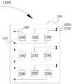
在本发明的一个方面,本发明的一个目的在于提出一种可灵活进行操作的纳米纸。具体地,参考图1,该纳米纸1000包括透明衬底100,以及位于透明衬底100上的多个压力传感单元200。透明衬底包括微纳纤维,因而具有较高的光透过率以及较好的柔性。多个压力传感单元200均位于透明衬底100的同一侧,且压力传感单元200的电阻可随着透明衬底100发生形变而改变。由此,当该纳米纸表面受到压力触控,例如书写、标记、作画等操作,则多个压力传感单元即可根据书写的轨迹,以及书写的力度(即纳米纸表面所受到的压力),记录书写内容,从而实现图形的处理。该纳米纸还包括多个导线300,多个导线300与压力传感单元200相连,且被配置为可单独输出多个压力传感单元200中的每一个的传感信号。由此,该纳米纸可以对作用于其表面的压力进行传感,且采用透明衬底可提高该纳米纸的整体透过率,可以将该纳米纸置于电子设备的显示屏上方,结合显示屏显示的图形进行操作。In one aspect of the present invention, an object of the present invention is to propose a nanopaper that can be operated flexibly. Specifically, referring to FIG. 1 , the
下面,根据本发明的具体实施,对该纳米纸实现上述有益效果的原理,以及该纳米纸的具体结构进行详细说明:Below, according to the specific implementation of the present invention, the principle of realizing the above-mentioned beneficial effects of the nano-paper and the specific structure of the nano-paper will be described in detail:
根据本发明的实施例,透明衬底100可以是由透明的柔性、可实现自支撑的材料形成的。例如,可以采用具有微米或是纳米尺寸的纤维形成的纸张。由于形成纸张的纤维的直径在纳米级别,因此,与常规的纸张相比,纳米纸具有更好的光透过率以及柔性。压力传感单元200可以具有压力传感层,压力传感层是由层状纳米材料形成的。具体地,层状纳米材料可以为具有层状结构的半导体材料。例如,压力传感层可以包括石墨烯、MoS2,WS2,MoSe2以及WSe2的至少之一。上述层状半导体材料由于具有层状的微观结构,多层材料之间的间距随着透明衬底发生形变而改变。具有层状结构的半导体材料中的电子多沿着层状平面流通,因而层状平面之间间距的改变,可改变材料整体的电阻,从而可以依据压力传感单元的压力传感层的电阻的变化,判断出纳米纸的何处受到了压力,并根据电阻改变的情况,可判断出压力的大小。并且,由于该过程是基于透明衬底发生形变而带来的,因此,无需理由特殊的触控笔对纳米纸表面进行操作,任何可传递压力的物体均可造成压力传感层的感应。由此,可以确定在该纳米纸上进行书写的内容,以及书写的压力。并且,层状半导体材料由于材料的特性,因此柔性较好,并且,上述层状材料的透过率也较高,因此采用上述材料形成压力传感层,也可提高该纳米纸的整体透光性能,进而可以进一步提高该压力传感单元的压力传感效果。According to an embodiment of the present invention, the
根据本发明的实施例,压力传感单元200的数量、在透明衬底100上排布的具体方式不受特别限制,只要能够在纳米纸表面实现书写轨迹的传感即可,本领域技术人员可以根据该纳米纸对于书写精度的要求进行设计。例如,可以令多个压力传感单元200在透明衬底100上阵列排布。本领域技术人员能够理解的是,该纳米纸使用时,需要将压力传感的结果发送至电子设备中,进而实现根据压力传感结果进行诸如图形的处理,因此纳米纸多需要配合具有显示功能的电子设备使用。此时,压力传感单元200的数量,可以与电子设备的显示屏中的像素的数量相等,由此,可实现与显示屏像素相匹配的压力传感精度,从而可以进一步提高进行图形处理的效果。According to the embodiment of the present invention, the number of the
根据本发明的实施例,透明衬底100上还可以具有与压力传感单元相连的导线300,导线300被配置为可独立地输出多个压力传感单元200中的每一个的压力传感信号。由此,可以对具有压力传感单元200的多个位点进行独立地压力感应,从而进一步提高该纳米纸记录书写轨迹以及力度的精确程度。具体地,该纳米纸可以进一步包括多个连接端口,通过多个连接端口以及导线300之间的配合,单独地输出多个压力传感单元200的传感信号。如前所述,压力传感单元200在受到压力时,压力传感层的电阻会发生改变。因此,单独输出每个压力传感单元200的传感信号仅需能够检测每个压力传感单元的电阻变化即可。According to an embodiment of the present invention, the
根据本发明一些具体的实施例,压力传感单元200可以在透明衬底100上阵列排布,即排列成多行以及多列。由此,一方面规则的排布方式可以简化制备压力传感单元200的工艺,另一方面阵列排布的压力传感单元也可以与电子设备的显示屏中子像素的排布方式相匹配,从而进一步提高利用该电子纸进行书写的效果。此时,参考图1,透明衬底100上可以具有多个第一连接端口410,每个第一连接端口410可以通过导线300与位于同一行的多个压力传感单元300均相连。同时,每个压力传感单元200均可对应连接有一个第二连接端口420。也即是说,每个压力传感单元200均与两个连接端口相连,位于同一行的多个压力传感单元连接至一个第一连接端口410,同时每个压力传感单元200还连接有一个仅与该压力传感单元200相连的第二连接端口420(如图中所示出的420A以及420B)。由此,可通过第一连接端口410和第二连接端口420单独地输出每个压力传感单元200的电阻变化情况。本领域技术人员能够理解的是,第一连接端口410和第二连接端口420的设置是为了利用尽可能少的连接端口,实现每个压力传感单元200的信号的单独输出。需要特别说明的是,为了方便理解,图1中仅示出了一种第一连接端口410以及第二连接端口420的排列方式,而不能够认为该种排列方式是对本发明的限制。例如,第一连接端口也可以与位于同一列的多个压力传感单元200均相连。由此,可简便地单独输出每个压力传感单元的传感信号,从而进一步提高该压力传感单元的灵敏度。According to some specific embodiments of the present invention, the
根据本发明的实施例,纳米纸的透过率可以高于90%。由此,该纳米纸具有较高的透过率,可通过将该纳米纸置于显示屏上方,结合显示屏显示的画面进行书写。为了提高纳米纸的透过率,可控制形成压力传感单元200的压力传感层的层状材料所包含的层数,提高压力传感单元200的透过率。导线300可以有诸如ITO等透明导电材料形成,从而可以减低走线300对于透过率的影响。第一连接端口以及第二连接端口可设置于透明衬底的边缘。由此,可尽可能的减小对于中心区域透过率的影响。According to an embodiment of the present invention, the transmittance of the nanopaper may be higher than 90%. Therefore, the nanopaper has high transmittance, and writing can be performed by placing the nanopaper above the display screen and combining with the picture displayed by the display screen. In order to improve the transmittance of the nanopaper, the number of layers included in the layered material forming the pressure sensing layer of the
根据本发明的实施例,为了进一步提高该纳米纸的使用功能,参考图2,该纳米纸还可以进一步包括电源模块500,电源模块500与压力传感单元200电连接,可为压力传感单元200供电,从而无需额外接入电源即可使用。特别是当该纳米纸与电子设备结合进行图形处理时,纳米纸可以无需电子设备供电。为了方便压力传感数据的传输,该纳米纸还可以具有蓝牙传输模块600。蓝牙传输模块600被配置为可接收多个压力传感单元中的每一个的传感信号。由此,可通过蓝牙无线传输,将该纳米纸的压力传感信号发送至电子设备,从而实现诸如图形处理等功能。According to an embodiment of the present invention, in order to further improve the use function of the nanopaper, referring to FIG. 2 , the nanopaper may further include a
根据本发明的一些实施例,参考图3,为了进一步提高该纳米纸的使用性能,防止在进行书写时由于纳米纸发生移动、折皱等情况,导致对书写轨迹检测的不准确,在透明衬底100未设置压力传感单元200的一侧,还可以具有固定胶层700。具体地,固定胶层700在透明衬底上100的投影可以位于透明衬底100的边缘处,且固定胶层700远离透明衬底100一侧的表面具有粘性。由此,可以利用固定胶层700将其固定在较为平整的表面,例如可以为电子设备的显示屏上。固定胶层700与透明衬底100相接触的一侧可具有较大的粘度,而远离透明衬底100的一侧可具有较小的粘度。由此,通过固定胶层700,可令该纳米纸具有类似于便利贴的功能,在需要贴附固定时可依靠粘度较小的一侧贴在较为平整的表面上,使用后由于远离透明衬底100一侧的粘度较小,因此可以在不损伤纳米纸的前提下,将纳米纸由屏幕上揭除。存放纳米纸时,仅需在固定胶层700远离透明衬底100一侧设置诸如离型膜或是离型纸等结构即可。固定胶层700可不覆盖透明衬底100的全部表面,只要能够起到固定作用即可。According to some embodiments of the present invention, referring to FIG. 3 , in order to further improve the usability of the nanopaper and prevent inaccurate detection of the writing track due to the movement and wrinkling of the nanopaper during writing, the transparent substrate The side of the 100 where the
在本发明的又一方面,本发明提出了一种利用前面所述的纳米纸进行图形处理的方法。根据本发明的实施例,该方法可以包括以下步骤:将纳米纸置于电子设备的显示屏上,并在纳米纸上进行书写等操作。利用纳米纸的压力传感单元,记录对纳米纸表面进行的图形处理信号(由书写操作产生)。该图形处理信号包括压力运动轨迹信号以及按压压力信号的至少之一。随后,将上述图形处理信号发送至电子设备,以便电子设备基于所述图形处理信号进行图形处理。该方法可以利用结构简单的纳米纸进行图形处理,且可利用纳米纸进行压力传感,从而记录书写的轨迹以及笔记的压力。由此,可通过简单的触控,实现对电子设备中的图形进行处理。In yet another aspect of the present invention, the present invention provides a method for pattern processing using the aforementioned nanopaper. According to an embodiment of the present invention, the method may include the following steps: placing the nanopaper on the display screen of the electronic device, and performing operations such as writing on the nanopaper. Using the pressure sensing unit of the nanopaper, the patterning signal (generated by the writing operation) performed on the surface of the nanopaper is recorded. The graphic processing signal includes at least one of a pressure movement track signal and a pressing pressure signal. Then, the above-mentioned graphics processing signal is sent to the electronic device, so that the electronic device performs graphics processing based on the graphics processing signal. The method can use nanopaper with a simple structure for graphic processing, and can use nanopaper for pressure sensing, so as to record the trajectory of writing and the pressure of notes. Therefore, the graphics in the electronic device can be processed through a simple touch.
下面,根据本发明的具体实施例,对上述图形处理的方法的具体操作进行详细说明。Hereinafter, specific operations of the above-mentioned graphics processing method will be described in detail according to specific embodiments of the present invention.
如前所述,前述的纳米纸可以记录纳米纸表面受到的压力的轨迹以及压力的压力值。并且,鉴于根据本发明实施例的纳米纸具有较高的透过率,因此可置于电子设备的上方,基于电子设备显示屏幕显示的画面的特定位置,进行书写、批注等操作。上述书写、批注等操作均可以通过压力传感单元进行记录。上述传感结果即为图形处理信号。将该信号传输至电子设备,即可基于该图形处理信号,对电子设备中存储的图形进行修改处理。As mentioned above, the aforementioned nanopaper can record the trajectory of the pressure on the surface of the nanopaper and the pressure value of the pressure. Moreover, in view of the high transmittance of the nanopaper according to the embodiment of the present invention, it can be placed above the electronic device, and operations such as writing and annotation can be performed based on a specific position of the picture displayed on the display screen of the electronic device. The above operations such as writing and annotation can be recorded by the pressure sensing unit. The above sensing result is the graphic processing signal. By transmitting the signal to the electronic device, the graphics stored in the electronic device can be modified based on the graphics processing signal.
需要特别说明的是,在本申请中,“图形处理”应做广义理解,其即包括对图画进行的处理,也包括对文字进行的处理:对纳米纸而言,图画和文字仅在压力感应的轨迹上有所不同,而不会对压力传感的过程造成影响。类似地,对于电子设备而言,对特定的显示画面进行有关图画或是有关文字的修改,也仅为显示内容上的差异,而不会对具体的处理方法造成影响。也即是说,本申请所述的图形处理方法,既可以包括对图画进行的处理,也可以包括诸如增加批注、删除文字等处理。It should be noted that, in this application, "graphic processing" should be understood in a broad sense, which includes both the processing of pictures and the processing of words: for nanopaper, pictures and words are only sensitive to pressure. trajectories without affecting the pressure sensing process. Similarly, for an electronic device, the modification of pictures or texts on a specific display screen is only a difference in the display content, and does not affect the specific processing method. That is to say, the graphics processing method described in this application may include not only processing on pictures, but also processing such as adding annotations and deleting characters.
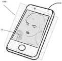
根据本发明的实施例,基于图形处理信号进行图形处理可以是第一处理模式下,利于电子设备,基于图形处理信号在需要进行处理的图形中增加图形内容。具体地,参考图4,可将纳米纸1000置于电子设备2000的显示屏上方,此时显示屏可用于显示需要进行处理的图形,如图中所示出的人像。此时可利用诸如用户的手指、尖端不过于尖锐的物体(如不具有书写功能的笔)等物体,在纳米纸1000的表面进行书写或是绘画,以在需要进行处理的图形上对应的位置处,形成想要增加的图形内容1A,如图4中所示出的花朵。在纳米纸上进行绘制时,可以通过记录压力改变的轨迹,记录增加的图形的形状,例如构成花朵的线条。而线条颜色的深浅、粗细,可以通过压力数值体现:书写越用力,则压力传感器受到的压力值越大,在传感数据发送至电子设备的处理器之后,处理器可根据压力值确定线条的粗细,或线条颜色的深浅。确定了增加图形内容的位置、线条、颜色、线宽等参数之后,增加的图形内容也即随之而确定。由此,处理器可在图形(人像)中增加特定的图形,例如图4中所示出的花朵。According to an embodiment of the present invention, performing graphics processing based on the graphics processing signal may be in the first processing mode, which is beneficial to the electronic device, and adding graphics content to the graphics to be processed based on the graphics processing signal. Specifically, referring to FIG. 4 , the
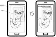
类似地,根据本发明的实施例,该方法还可以用于改变图形中特定位置的颜色。例如,参考图5,可首先通过对电子设备进行操作,例如在应用程序中选择改变颜色的模式,随后在纳米纸的特定位置进行类似于填色的操作,例如,当想改变图5中所显示的人像的唇部(如图中所示出的1B)颜色时,可利用手指或是笔,在纳米纸上的相应位置进行操作。由于纳米纸1000具有较高的透过率,因此在进行操作时,用户可透过纳米纸观察到电子设备的显示屏中所显示的内容,从而可以准确的确定进行操作的区域。此时利用纳米纸记录进行操作的具体位置,以及操作的压力,将图形处理信号传输至电子设备之后,处理器可根据操作的具体位置,对图形中相应区域的颜色进行处理,令显示的图形特定区域的颜色发生改变。并且,还可以根据触控的压力数值,确定不同位置增加的颜色的深度。Similarly, according to an embodiment of the present invention, the method can also be used to change the color of a specific location in a graph. For example, referring to FIG. 5, you can first operate the electronic device, such as selecting a mode to change the color in an application, and then perform a color-filling operation at a specific position of the nanopaper. For example, when you want to change the color in FIG. 5 When the color of the lips of the portrait (as shown in 1B in the figure) is displayed, you can use a finger or a pen to operate the corresponding position on the nanopaper. Since the
类似地,根据本发明的实施例,该方法还可以用于删除图形中的特定内容。即:在第二处理模式下,电子设备基于图形处理信号对需要进行处理的图形进行擦除处理。例如,可通过应用软件等,选择橡皮擦模式,随后对需要擦除的区域进行触摸。当触摸的路径(即压力运动轨迹信号)传输至电子设备的处理器中之后,处理器即可对该位置处的图形内容进行删除。根据本发明的另一些实施例,还可以记录进行触摸的压力,不同的压力数值区间,可以对应擦除操作的深浅:即,当用力较大时,可对进行操作区域的内容进行完全的删除。触摸力度较小时,可令该区域的图形内容变淡,此时不对该区域的图形进行完全删除,而是令该区域的透过率增高,进而表现出图形内容变淡的视觉效果。可以将纳米纸受到的压力进行分级,不同分级下,处理后图形特定区域的透过率(或称为透明度)也不同。由此,可利用该方法进行丰富的图形处理操作。需要特别说明的是,上述删除内容或是令图形中特定区域显示内容变淡的具体方式不受特别限制,上述将压力和图形显示内容的透过率均进行分级的方式仅为一种实现形式,而不能理解为对本发明的限制。例如,也可以不对压力和透过率进行分级,而是绘制压力数值和透过率的标准曲线,再依据纳米纸受到的压力数值,确认压力运动轨迹上每一点所对应的透过率,再根据该透过率对图形进行处理。Similarly, according to an embodiment of the present invention, the method can also be used to delete specific content in the graphics. That is, in the second processing mode, the electronic device performs erasing processing on the graphics to be processed based on the graphics processing signal. For example, the eraser mode can be selected through application software or the like, and then the area to be erased can be touched. After the touch path (ie, the pressure movement track signal) is transmitted to the processor of the electronic device, the processor can delete the graphic content at the position. According to other embodiments of the present invention, the pressure of the touch can also be recorded, and different pressure value intervals can correspond to the depth of the erasing operation: that is, when the force is large, the content of the operation area can be completely deleted . When the touch force is small, the graphic content in the area can be faded. At this time, the graphic in the area is not completely deleted, but the transmittance of the area is increased, thereby showing the visual effect of the graphic content being faded. The pressure on the nanopaper can be graded, and under different grades, the transmittance (or transparency) of a specific area of the processed pattern is also different. Thus, rich graphics processing operations can be performed using this method. It should be noted that the specific method of deleting the content or making the display content of a specific area in the graph lighten is not particularly limited, and the above-mentioned method of grading both the pressure and the transmittance of the graph display content is only an implementation form. , and should not be construed as a limitation of the present invention. For example, instead of grading pressure and transmittance, draw a standard curve of pressure value and transmittance, and then confirm the transmittance corresponding to each point on the pressure movement trajectory according to the pressure value of the nanopaper. Graphics are processed according to the transmittance.
根据本发明的实施例,上述对图形进行处理的方法需利用纳米纸以及电子设备来实现,电子设备的显示屏可以为触控显示屏。此时为了防止用户在对纳米纸进行操作的过程中,误启动触控显示屏的触控功能,可以在对纳米纸进行操作之前,通过包括但不限于应用软件等方式,停止触控显示屏的触控传感器对于纳米纸所在区域的触控传感。According to an embodiment of the present invention, the above-mentioned method for processing graphics needs to be implemented by using nanopaper and an electronic device, and the display screen of the electronic device may be a touch display screen. At this time, in order to prevent the user from accidentally starting the touch function of the touch screen during the operation of the nanopaper, the touch screen can be stopped by means including but not limited to application software before operating the nanopaper. touch sensor for the touch sensing of the area where the nanopaper is located.
根据本发明的实施例,纳米纸的面积可以小于所述电子设备的显示屏的面积。此时,在对纳米纸进行操作之前,该方法还可以进一步包括对需要进行图形处理的区域进行校正的步骤。具体地,参考图6,电子设备的显示屏可以为触控显示屏,上述校正可以是通过以下步骤实现的:将纳米纸固定在触控显示屏中需要进行图形处理的位置,如图6中所示出的,纳米纸1000由于尺寸较小,因此仅能覆盖显示内容的一部分(如图中所述示出的,覆盖卡通图形的上方一部分区域)。此时可在显示需要处理的图形的同时,利用触控显示屏同时显示可拖动并可改变大小的选择框。用户在纳米纸上进行操作之前,预先对触控显示屏进行操作,缩小选择框至和纳米纸1000大小相等,并拖动选择框,使选择框的边缘与纳米纸吻合。由此,触控屏可根据用户对于选择框的操作,确定纳米纸固定的区域,后续在接收到纳米纸1000的图形处理信号之后,再根据该信号对特定区域(选择框选定的区域)进行图形处理。According to an embodiment of the present invention, the area of the nanopaper may be smaller than that of the display screen of the electronic device. At this time, before the operation on the nanopaper, the method may further include the step of correcting the area that needs to be patterned. Specifically, referring to FIG. 6 , the display screen of the electronic device can be a touch display screen, and the above correction can be achieved by the following steps: fixing the nanopaper in the position where graphics processing needs to be performed in the touch display screen, as shown in FIG. 6 . As shown, due to its small size, the
或者,参考图7,对需要进行图形处理的区域进行校正也可以是通过以下步骤实现的:在利用纳米纸进行图形处理之前,首先利用触控显示屏显示需要处理的图形,且该图形中包括定位确认位点,如图中所示出的A点。随后,将纳米纸固定在显示屏上。由于纳米纸具有较好的透过率,此时显示屏上显示的图形仍是对用户可见的。此时用户可以触碰纳米纸表面与显示屏上的确认位点A相对应的位置,如图中所示出的A’。由此,可在将图形处理信号传输至电子设备的处理器中之后,令纳米纸上感应的A’点与定位确认位点A对应,以完成图形处理的区域的校正。根据本发明的一些实施例,上述定位确认位点可以为1个,也可以为多个。Alternatively, referring to FIG. 7 , the correction of the area that needs to be processed by graphics can also be achieved by the following steps: before using the nanopaper for graphics processing, first use the touch screen to display the graphics to be processed, and the graphics include Locate the confirmation site, as indicated by point A in the figure. Then, the nanopaper is fixed on the display screen. Since the nanopaper has better transmittance, the graphics displayed on the display screen are still visible to the user at this time. At this time, the user can touch the position of the nanopaper surface corresponding to the confirmation point A on the display screen, as shown in the figure A'. Therefore, after the graphic processing signal is transmitted to the processor of the electronic device, the A' point sensed on the nanopaper can be made to correspond to the positioning confirmation point A, so as to complete the correction of the graphic processing area. According to some embodiments of the present invention, there may be one or more than one location confirmation site.
在本发明的另一些实施例中,对需要进行图形处理的区域进行校正还可以是通过以下步骤实现的:将纳米纸置于显示屏上方之后,可以令显示屏贴附有纳米纸的区域对触控无反应。此时,可利用手指等,对显示屏贴附有纳米纸的区域以及纳米纸边缘周围的区域进行来回触控。此时,具有纳米纸的区域对触控无响应,而纳米纸边缘周围的区域,可感应到手指的触控。由此,可利用手指的触控区域,确定处一个中空的、对触控无感的区域,该区域即对应纳米纸所在的区域。由此,可实现图形处理区域的校正。In other embodiments of the present invention, the correction of the area that needs to be subjected to graphic processing can also be achieved by the following steps: after placing the nanopaper on the display screen, the area of the display screen with the nanopaper attached can be adjusted Touch does not respond. At this time, a finger or the like can be used to touch back and forth the area where the nanopaper is attached to the display screen and the area around the edge of the nanopaper. At this time, the area with the nanopaper does not respond to touch, while the area around the edge of the nanopaper can sense the touch of the finger. Therefore, the touch area of the finger can be used to determine a hollow area that is insensitive to touch, and this area corresponds to the area where the nanopaper is located. Thereby, correction of the graphics processing area can be realized.
在本发明中,仅列出了一部分进行图形处理的具体实施例。实际上本领域技术人员能够理解的是,只要是能够根据纳米纸所记录的图形处理信号进行的操作,均可利用上述方法实现图形的处理。也即是说,只要能够根据对纳米纸表面进行操作的压力运动轨迹,以及按压压力信号进行的图形处理,则均可采用本发明所提出的方法实现。例如,根据本发明实施例的方法还可实现类似于临摹图形的功能:以书法作品的临摹为例,在书写或作画时,作品的力度、下笔轨迹及停留的时间均对最终的作品具有重要影响。可通过纳米纸记录用户的书写习惯,并通过电子设备以及应用程序,帮助分析用笔错误或需要改进的地方。更具体地,对于书写而言下笔不能太重,否则字迹会多肉少骨,字体“发软”。运笔也不能太慢,要掌握节奏。而根据本申请实施例的纳米纸可以记录用户运笔的轨迹、力度(按压压力值),因此可在电子设备中添加类似于教学程序的应用软件,将压力分级,做成图谱,使用户更好的体会怎样才能正确流畅的进行书写或作画。也可以利用电子设备的显示屏显示书法或是绘画作品,用户在纳米纸的界面进行临摹,临摹的作品可保存在电子设备中,便于对比:具体地,可以在电子设备中,将用户在纳米纸上进行临摹操作所产生的图形处理信号与电子设备中存储的标准信号(即用户进行临摹的原作)进行比对,并基于比对结果,生成临摹图形。临摹图形为基于标准信号形成的图形(原作),和基于图形处理信号形成的图形(用户临摹的结果)的叠加图形。由此,可简便地显示用户临摹作品与原作之间的差异,可更好地提升用户书画的水平。In the present invention, only a part of specific embodiments for performing graphics processing are listed. In fact, those skilled in the art can understand that, as long as the operation can be performed according to the graphic processing signal recorded by the nanopaper, the above-mentioned method can be used to realize the graphic processing. That is to say, as long as the trajectory of the pressure movement performed on the surface of the nanopaper and the graphic processing of the pressing pressure signal can be performed, the method proposed in the present invention can be used. For example, the method according to the embodiment of the present invention can also realize a function similar to copying graphics: take copying of a calligraphy work as an example, when writing or painting, the strength of the work, the trajectory of the stroke and the time of staying are all important to the final work. influences. The user's writing habits can be recorded through nanopaper, and electronic devices and applications can help analyze pen mistakes or areas that need improvement. More specifically, the pen should not be too heavy for writing, otherwise the handwriting will be fleshy and boneless, and the font will be "soft". The pen movement should not be too slow, and the rhythm should be mastered. However, the nanopaper according to the embodiment of the present application can record the trajectory and strength (pressing pressure value) of the user's pen movement. Therefore, an application software similar to a teaching program can be added to the electronic device, and the pressure can be classified into a map, so that the user can better The experience of how to write or draw correctly and fluently. It is also possible to use the display screen of the electronic device to display calligraphy or painting works, and the user can copy on the interface of the nano-paper, and the copied works can be saved in the electronic device for easy comparison: specifically, in the electronic device, the user can be placed in the nano-paper. The graphic processing signal generated by the copying operation on the paper is compared with the standard signal stored in the electronic device (that is, the original copy copied by the user), and based on the comparison result, a copying graphic is generated. The copied graphic is a superimposed graphic formed based on a standard signal (original work) and a graphic formed based on a graphic processing signal (the result of the user's copying). Thereby, the difference between the user's copy work and the original work can be easily displayed, and the user's calligraphy and painting level can be better improved.
在本发明的另一方面,本发明提出了一种制备纳米纸的方法。根据本发明的实施例,该方法制备的纳米纸可以为前述的纳米纸。因此该方法获得的纳米纸具有和前述纳米纸相同的特征以及优点,在此不再赘述。具体而言,该方法可以包括:提供透明衬底,并在透明衬底上形成多个压力传感单元以及多个导线。压力传感单元的电阻可随着所述透明衬底发生形变而改变,并可通过所述导线单独输出多个所述压力传感单元中的每一个的传感信号。由此,可简便地获得结构简便的纳米纸。In another aspect of the present invention, the present invention provides a method for preparing nanopaper. According to an embodiment of the present invention, the nanopaper prepared by the method can be the aforementioned nanopaper. Therefore, the nanopaper obtained by this method has the same features and advantages as the aforementioned nanopaper, which will not be repeated here. Specifically, the method may include: providing a transparent substrate, and forming a plurality of pressure sensing units and a plurality of wires on the transparent substrate. The resistance of the pressure sensing unit can be changed as the transparent substrate is deformed, and a sensing signal of each of the plurality of pressure sensing units can be individually output through the wire. Thereby, nanopaper with a simple structure can be easily obtained.
根据本发明一些具体实施例,制备该纳米纸的方法可以包括:选用由具有纳米级直径的纤维构成的透明纳米纸为透明衬底,通过设置掩膜版并蒸镀金属的方式,首先形成多个导线。多个导线的排列以及位置可以为前面描述的,在此不再赘述。需要特别说明的是,此处蒸镀的金属需控制金属厚度,在实现导电功能的前提下,尽可能将导线的厚度控制在较小的范围内,以防对该纳米纸的整体透过率产生负面影响。随后,去除掩膜版,采用另一张用于形成压力传感单元的掩膜,在形成有导线的透明衬底上,形成由石墨烯构成的压力传感单元。由此,可简便地形成上述纳米纸。According to some specific embodiments of the present invention, the method for preparing the nanopaper may include: selecting transparent nanopaper composed of fibers with nanometer diameters as a transparent substrate, and by setting a mask and evaporating metal, firstly forming a multi-layered nanopaper. a wire. The arrangement and position of the plurality of wires may be as described above, and will not be repeated here. It should be noted that the thickness of the metal evaporated here needs to be controlled. On the premise of realizing the conductive function, the thickness of the wire should be controlled within a small range as much as possible to prevent the overall transmittance of the nanopaper. result in negative effect. Then, the mask is removed, and another mask for forming the pressure sensing unit is used to form the pressure sensing unit composed of graphene on the transparent substrate formed with the wires. Thereby, the above-mentioned nanopaper can be easily formed.
在本发明的又一方面,本发明提出了一种电子设备。该电子设备包括显示屏以及主板,主板与显示屏电连接。该电子设备还配备有前面所述的纳米纸,纳米纸可揭除地位于显示屏上,且纳米纸被配置为可向主板输出多个压力传感单元的传感信号。由此,该电子设备具有前述的纳米纸所具有的全部特征以及优点,在此不再赘述。总的来说,该纳米纸可以对作用于其表面的压力进行传感,且采用透明衬底可提高该纳米纸的整体透过率,可以将该纳米纸置于电子设备的显示屏上方,结合显示屏显示的图形进行操作。In yet another aspect of the present invention, the present invention provides an electronic device. The electronic device includes a display screen and a main board, and the main board is electrically connected with the display screen. The electronic device is also equipped with the aforementioned nano-paper, the nano-paper is detachably located on the display screen, and the nano-paper is configured to output the sensing signals of the plurality of pressure sensing units to the main board. Therefore, the electronic device has all the features and advantages of the aforementioned nanopaper, which will not be repeated here. In general, the nanopaper can sense the pressure acting on its surface, and the use of a transparent substrate can improve the overall transmittance of the nanopaper, and the nanopaper can be placed above the display screen of electronic equipment, Operates in conjunction with the graphics displayed on the display.
在本发明的描述中,术语“上”、“下”、“内”、“外”等指示的方位或位置关系为基于附图所示的方位或位置关系,仅是为了便于描述本发明而不是要求本发明必须以特定的方位构造和操作,因此不能理解为对本发明的限制。In the description of the present invention, the orientation or positional relationship indicated by the terms "upper", "lower", "inner", "outer", etc. is based on the orientation or positional relationship shown in the accompanying drawings, which is only for the convenience of describing the present invention. It is not a requirement that the present invention be constructed and operated in a particular orientation and is therefore not to be construed as a limitation of the present invention.
在本说明书的描述中,参考术语“一个实施例”、“另一个实施例”等的描述意指结合该实施例描述的具体特征、结构、材料或者特点包含于本发明的至少一个实施例中。在本说明书中,对上述术语的示意性表述不必须针对的是相同的实施例或示例。而且,描述的具体特征、结构、材料或者特点可以在任一个或多个实施例或示例中以合适的方式结合。此外,在不相互矛盾的情况下,本领域的技术人员可以将本说明书中描述的不同实施例或示例以及不同实施例或示例的特征进行结合和组合。另外,需要说明的是,本说明书中,术语“第一”、“第二”仅用于描述目的,而不能理解为指示或暗示相对重要性或者隐含指明所指示的技术特征的数量。In the description of this specification, description with reference to the terms "one embodiment", "another embodiment", etc. means that a particular feature, structure, material or characteristic described in connection with the embodiment is included in at least one embodiment of the present invention . In this specification, schematic representations of the above terms are not necessarily directed to the same embodiment or example. Furthermore, the particular features, structures, materials or characteristics described may be combined in any suitable manner in any one or more embodiments or examples. Furthermore, those skilled in the art may combine and combine the different embodiments or examples described in this specification, as well as the features of the different embodiments or examples, without conflicting each other. In addition, it should be noted that in this specification, the terms "first" and "second" are only used for description purposes, and cannot be understood as indicating or implying relative importance or implicitly indicating the number of indicated technical features.
尽管上面已经示出和描述了本发明的实施例,可以理解的是,上述实施例是示例性的,不能理解为对本发明的限制,本领域的普通技术人员在本发明的范围内可以对上述实施例进行变化、修改、替换和变型。Although the embodiments of the present invention have been shown and described above, it should be understood that the above-mentioned embodiments are exemplary and should not be construed as limiting the present invention. Embodiments are subject to variations, modifications, substitutions and variations.
Claims (12)
Translated fromChinesePriority Applications (3)
| Application Number | Priority Date | Filing Date | Title |
|---|---|---|---|
| CN201910537795.2ACN110273322B (en) | 2019-06-20 | 2019-06-20 | Nano paper, preparation method, method for carrying out graphic processing and electronic equipment |
| PCT/CN2020/096569WO2020253720A1 (en) | 2019-06-20 | 2020-06-17 | Nano paper and preparation method, method for image processing and electronic device |
| US17/420,962US11630531B2 (en) | 2019-06-20 | 2020-06-17 | Nano paper and preparation method, method for image processing and electronic device |
Applications Claiming Priority (1)
| Application Number | Priority Date | Filing Date | Title |
|---|---|---|---|
| CN201910537795.2ACN110273322B (en) | 2019-06-20 | 2019-06-20 | Nano paper, preparation method, method for carrying out graphic processing and electronic equipment |
Publications (2)
| Publication Number | Publication Date |
|---|---|
| CN110273322A CN110273322A (en) | 2019-09-24 |
| CN110273322Btrue CN110273322B (en) | 2022-04-26 |
Family
ID=67962262
Family Applications (1)
| Application Number | Title | Priority Date | Filing Date |
|---|---|---|---|
| CN201910537795.2AActiveCN110273322B (en) | 2019-06-20 | 2019-06-20 | Nano paper, preparation method, method for carrying out graphic processing and electronic equipment |
Country Status (3)
| Country | Link |
|---|---|
| US (1) | US11630531B2 (en) |
| CN (1) | CN110273322B (en) |
| WO (1) | WO2020253720A1 (en) |
Families Citing this family (3)
| Publication number | Priority date | Publication date | Assignee | Title |
|---|---|---|---|---|
| CN110273322B (en)* | 2019-06-20 | 2022-04-26 | 京东方科技集团股份有限公司 | Nano paper, preparation method, method for carrying out graphic processing and electronic equipment |
| CN111477066A (en)* | 2020-04-02 | 2020-07-31 | 中科院合肥技术创新工程院 | A method, device and system for calligraphy practice based on multi-array pressure sensor |
| CN116009757A (en)* | 2021-10-20 | 2023-04-25 | 京东方科技集团股份有限公司 | Touch display method and device, computer-readable storage medium, electronic device |
Citations (10)
| Publication number | Priority date | Publication date | Assignee | Title |
|---|---|---|---|---|
| CN1945516A (en)* | 2005-07-08 | 2007-04-11 | 哈拉尔德·菲利普 | Two-dimensional position sensor |
| CN101836178A (en)* | 2007-10-26 | 2010-09-15 | 安德烈亚斯·施泰因豪泽 | Touch screen or touchpad with single-touch or multi-touch capability comprising an array of pressure sensors and fabrication of such sensors |
| CN102763055A (en)* | 2010-01-06 | 2012-10-31 | 苹果公司 | Transparent electronic device |
| CN103488415A (en)* | 2013-05-14 | 2014-01-01 | 高永杰 | Handwritten text and graphic recognition system based on paper medium and recognition method |
| CN104750273A (en)* | 2015-03-16 | 2015-07-01 | 联想(北京)有限公司 | Electronic equipment |
| CN105094425A (en)* | 2015-07-17 | 2015-11-25 | 苏州诺菲纳米科技有限公司 | Touch sensor, preparation method thereof and display device provided with touch sensor |
| CN204863062U (en)* | 2015-06-17 | 2015-12-16 | 中国科学院苏州纳米技术与纳米仿生研究所 | A flexible sensor and speculum robot for speculum robot |
| CN106708327A (en)* | 2017-01-21 | 2017-05-24 | 宸鸿科技(厦门)有限公司 | Pressure sensor and display device |
| CN108277684A (en)* | 2018-01-23 | 2018-07-13 | 京东方科技集团股份有限公司 | A kind of nanometer paper, preparation method and flexible electronic device |
| CN208207773U (en)* | 2018-06-11 | 2018-12-07 | 山东蓝贝思特教装集团股份有限公司 | For the multivoltage output circuit of writing film selective erase and application |
Family Cites Families (16)
| Publication number | Priority date | Publication date | Assignee | Title |
|---|---|---|---|---|
| CN100395691C (en)* | 2005-09-14 | 2008-06-18 | 王学永 | Numeric stored handwritting pen |
| CN104035483B (en)* | 2013-03-04 | 2018-03-27 | 联想(北京)有限公司 | A kind of electronic equipment and a kind of display methods |
| CN103196955B (en) | 2013-04-10 | 2015-01-07 | 中国人民解放军国防科学技术大学 | Silicon carbide nano paper sensor as well as production method and application thereof |
| US10480126B2 (en)* | 2013-12-06 | 2019-11-19 | University Of Maryland At College Park | Super clear cellulose paper |
| CN103966907B (en)* | 2014-04-02 | 2016-08-10 | 上海大学 | A kind of flexible conductive paper based on nanocellulose and preparation method thereof |
| CN203909752U (en) | 2014-05-30 | 2014-10-29 | 南昌欧菲光科技有限公司 | Touch substrate and touch screen provided with touch substrate |
| CN106293290B (en)* | 2015-06-10 | 2023-08-29 | 宸鸿科技(厦门)有限公司 | touch device |
| CN105092118B (en)* | 2015-09-25 | 2017-10-20 | 东南大学 | One kind has highly sensitive flexible piezoresistive pressure sensor and preparation method thereof |
| RU2748559C2 (en)* | 2016-04-08 | 2021-05-26 | Петер КОЛАРОВ | Device for qualified electronic signature in the form of a stylus and the method of its application |
| US10209840B2 (en)* | 2016-04-20 | 2019-02-19 | Lg Innotek Co., Ltd. | Touch window and touch device |
| KR102543477B1 (en)* | 2016-06-10 | 2023-06-16 | 삼성디스플레이 주식회사 | Sensor and display device having the same |
| US10514797B2 (en) | 2017-04-18 | 2019-12-24 | Google Llc | Force-sensitive user input interface for an electronic device |
| CN207764760U (en) | 2017-12-13 | 2018-08-24 | 南昌欧菲显示科技有限公司 | Pressure sensitive module, touching display screen and touch-controlled electronic devices |
| CN108318059B (en) | 2018-02-12 | 2025-06-17 | 清华大学 | Paper-based sensor and preparation method thereof |
| EP3726191A1 (en)* | 2019-04-17 | 2020-10-21 | Nederlandse Organisatie voor toegepast- natuurwetenschappelijk Onderzoek TNO | Pressure sensor |
| CN110273322B (en) | 2019-06-20 | 2022-04-26 | 京东方科技集团股份有限公司 | Nano paper, preparation method, method for carrying out graphic processing and electronic equipment |
- 2019
- 2019-06-20CNCN201910537795.2Apatent/CN110273322B/enactiveActive
- 2020
- 2020-06-17WOPCT/CN2020/096569patent/WO2020253720A1/ennot_activeCeased
- 2020-06-17USUS17/420,962patent/US11630531B2/enactiveActive
Patent Citations (10)
| Publication number | Priority date | Publication date | Assignee | Title |
|---|---|---|---|---|
| CN1945516A (en)* | 2005-07-08 | 2007-04-11 | 哈拉尔德·菲利普 | Two-dimensional position sensor |
| CN101836178A (en)* | 2007-10-26 | 2010-09-15 | 安德烈亚斯·施泰因豪泽 | Touch screen or touchpad with single-touch or multi-touch capability comprising an array of pressure sensors and fabrication of such sensors |
| CN102763055A (en)* | 2010-01-06 | 2012-10-31 | 苹果公司 | Transparent electronic device |
| CN103488415A (en)* | 2013-05-14 | 2014-01-01 | 高永杰 | Handwritten text and graphic recognition system based on paper medium and recognition method |
| CN104750273A (en)* | 2015-03-16 | 2015-07-01 | 联想(北京)有限公司 | Electronic equipment |
| CN204863062U (en)* | 2015-06-17 | 2015-12-16 | 中国科学院苏州纳米技术与纳米仿生研究所 | A flexible sensor and speculum robot for speculum robot |
| CN105094425A (en)* | 2015-07-17 | 2015-11-25 | 苏州诺菲纳米科技有限公司 | Touch sensor, preparation method thereof and display device provided with touch sensor |
| CN106708327A (en)* | 2017-01-21 | 2017-05-24 | 宸鸿科技(厦门)有限公司 | Pressure sensor and display device |
| CN108277684A (en)* | 2018-01-23 | 2018-07-13 | 京东方科技集团股份有限公司 | A kind of nanometer paper, preparation method and flexible electronic device |
| CN208207773U (en)* | 2018-06-11 | 2018-12-07 | 山东蓝贝思特教装集团股份有限公司 | For the multivoltage output circuit of writing film selective erase and application |
Also Published As
| Publication number | Publication date |
|---|---|
| WO2020253720A1 (en) | 2020-12-24 |
| US20220100339A1 (en) | 2022-03-31 |
| CN110273322A (en) | 2019-09-24 |
| US11630531B2 (en) | 2023-04-18 |
Similar Documents
| Publication | Publication Date | Title |
|---|---|---|
| EP2369454B1 (en) | Handwritten input/output system, handwriting input sheet, information input system, and information input assistance sheet | |
| KR102061881B1 (en) | Multi display apparatus and method for controlling display operation | |
| CN110273322B (en) | Nano paper, preparation method, method for carrying out graphic processing and electronic equipment | |
| CN103729157A (en) | Multi-display apparatus and method of controlling the same | |
| EP2023237A1 (en) | Position indicating method and position indicating apparatus | |
| US20090052778A1 (en) | Electronic Annotation Of Documents With Preexisting Content | |
| JP2011123833A (en) | Information processing system and electronic pen | |
| US20170220140A1 (en) | Digital Cursor Display Linked to a Smart Pen | |
| WO2008150923A1 (en) | Customer authoring tools for creating user-generated content for smart pen applications | |
| KR101176104B1 (en) | Interactive electric board system and management method using optical sensing pen | |
| JP6146350B2 (en) | Information processing apparatus and computer program | |
| TW201732535A (en) | Method and apparatus that mimics the use of a flipchart using digital markers, touch input, and a low power reflective display | |
| JP2019067111A (en) | Display control device and program | |
| JP2011084050A (en) | Electronic writing system | |
| US12026326B2 (en) | Pen state detection circuit and method, and input system | |
| JP6528450B2 (en) | Handwriting input device | |
| JP6497266B2 (en) | Erase medium and handwriting input system | |
| JP6857867B2 (en) | Handwriting input sheet | |
| JP2015162161A (en) | Information processing apparatus, information processing program, and information processing method | |
| JP2012033130A (en) | Electronic writing pad | |
| KR101229296B1 (en) | Touch screen for handwriting recognition | |
| CN119473045A (en) | Data processing method and electronic device | |
| JP2017071136A (en) | Booklet and content creation system | |
| TWM572497U (en) | Writing pad | |
| JPH0575124B2 (en) |
Legal Events
| Date | Code | Title | Description |
|---|---|---|---|
| PB01 | Publication | ||
| PB01 | Publication | ||
| SE01 | Entry into force of request for substantive examination | ||
| SE01 | Entry into force of request for substantive examination | ||
| GR01 | Patent grant | ||
| GR01 | Patent grant |