CN110262149B - display panel - Google Patents
display panelDownload PDFInfo
- Publication number
- CN110262149B CN110262149BCN201910661077.6ACN201910661077ACN110262149BCN 110262149 BCN110262149 BCN 110262149BCN 201910661077 ACN201910661077 ACN 201910661077ACN 110262149 BCN110262149 BCN 110262149B
- Authority
- CN
- China
- Prior art keywords
- pixel electrode
- display panel
- hole
- insulating layer
- substrate
- Prior art date
- Legal status (The legal status is an assumption and is not a legal conclusion. Google has not performed a legal analysis and makes no representation as to the accuracy of the status listed.)
- Active
Links
- 239000000758substrateSubstances0.000claimsabstractdescription31
- 229910052751metalInorganic materials0.000claimsdescription8
- 239000002184metalSubstances0.000claimsdescription8
- 239000004973liquid crystal related substanceSubstances0.000description9
- 239000011159matrix materialSubstances0.000description5
- 239000004065semiconductorSubstances0.000description4
- 238000004519manufacturing processMethods0.000description2
- 229910021420polycrystalline siliconInorganic materials0.000description2
- 229920005591polysiliconPolymers0.000description2
- 229910052581Si3N4Inorganic materials0.000description1
- VYPSYNLAJGMNEJ-UHFFFAOYSA-NSilicium dioxideChemical compoundO=[Si]=OVYPSYNLAJGMNEJ-UHFFFAOYSA-N0.000description1
- 229910021417amorphous siliconInorganic materials0.000description1
- 239000004020conductorSubstances0.000description1
- 230000018109developmental processEffects0.000description1
- 239000012467final productSubstances0.000description1
- 239000011521glassSubstances0.000description1
- 230000012447hatchingEffects0.000description1
- AMGQUBHHOARCQH-UHFFFAOYSA-Nindium;oxotinChemical compound[In].[Sn]=OAMGQUBHHOARCQH-UHFFFAOYSA-N0.000description1
- 239000011810insulating materialSubstances0.000description1
- 239000000463materialSubstances0.000description1
- 238000000034methodMethods0.000description1
- 238000012986modificationMethods0.000description1
- 230000004048modificationEffects0.000description1
- 239000000047productSubstances0.000description1
- HQVNEWCFYHHQES-UHFFFAOYSA-Nsilicon nitrideChemical compoundN12[Si]34N5[Si]62N3[Si]51N64HQVNEWCFYHHQES-UHFFFAOYSA-N0.000description1
- 229910052814silicon oxideInorganic materials0.000description1
Images


Landscapes
- Liquid Crystal (AREA)
- Devices For Indicating Variable Information By Combining Individual Elements (AREA)
Abstract
Translated fromChinese
Description
Translated fromChinese本申请是中国发明专利申请(申请号:201510074956.0,申请日:2015年02月12日,发明名称:显示面板)的分案申请。This application is a divisional application of a Chinese invention patent application (application number: 201510074956.0, application date: February 12, 2015, invention name: display panel).
技术领域technical field
本发明涉及一种显示面板,且特别是涉及一种具有高分辨率的显示面板。The present invention relates to a display panel, and more particularly, to a display panel with high resolution.
背景技术Background technique
液晶显示器已被广泛地应用在各式电子产品,如手机、笔记型电脑(notebook)及平板电脑(Tablet PC)等,而且随着大尺寸平面显示器市场的快速发展,具有轻量化与薄型化特性的液晶显示器更是扮演着相当重要的角色,进而逐渐取代阴极射线管(CRT)显示器成为市场主流。Liquid crystal displays have been widely used in various electronic products, such as mobile phones, notebook computers (notebooks) and tablet computers (Tablet PCs), etc., and with the rapid development of the large-size flat-panel display market, it has the characteristics of light weight and thinning. The liquid crystal display plays a very important role, and gradually replaces the cathode ray tube (CRT) display to become the mainstream of the market.
并且,具有高分辨率的液晶显示器已经成为目前既定的趋势。然而,基于高分辨率所引入的新技术,也容易伴随衍生新的问题,而影响显示品质的问题。因此,如何提供一种具有良好显示品质且具有高分辨率的液晶显示面板,为相关业者努力的课题之一。And, the liquid crystal display with high resolution has become an established trend at present. However, the new technology introduced based on high resolution is also prone to generate new problems, which affect the display quality. Therefore, how to provide a liquid crystal display panel with good display quality and high resolution is one of the subjects that the related industry is working on.
发明内容SUMMARY OF THE INVENTION
本发明的目的在于提供一种显示面板。实施例中,第二像素电极相邻第一像素电极、且第二像素电极重叠共同电极的第一通孔的一部分,如此一来,可以有效缩短像素电极之间的距离,使得单位面积内可以设置较多数目的像素电极,因而可以有效提升显示面板的每英寸像素值(ppi)。An object of the present invention is to provide a display panel. In the embodiment, the second pixel electrode is adjacent to the first pixel electrode, and the second pixel electrode overlaps a part of the first through hole of the common electrode. In this way, the distance between the pixel electrodes can be effectively shortened, so that the unit area can be A larger number of pixel electrodes are provided, thereby effectively increasing the pixel value per inch (ppi) of the display panel.
为达上述目的,根据本发明的一实施例,提出一种显示面板。显示面板包括一第一基板、一晶体管元件、一第一绝缘层、一共同电极、一第二绝缘层、一第一像素电极以及一第二像素电极。扫描线位于第一基板上。晶体管元件位于第一基板上,并由扫描线所控制。第一绝缘层位于第一基板上。共同电极位于第一绝缘层上,且共同电极具有一第一通孔。第二绝缘层覆盖共同电极与部分的第一通孔。第一像素电极位于第二绝缘层上,且第一像素电极通过第一通孔且电连接于晶体管元件。第二像素电极位于第二绝缘层上,且第二像素电极相邻第一像素电极。扫描线与第二像素电极至少部分重叠,扫描线与第一像素电极不重叠。To achieve the above objective, according to an embodiment of the present invention, a display panel is provided. The display panel includes a first substrate, a transistor element, a first insulating layer, a common electrode, a second insulating layer, a first pixel electrode and a second pixel electrode. The scan lines are located on the first substrate. The transistor elements are located on the first substrate and controlled by the scan lines. The first insulating layer is on the first substrate. The common electrode is located on the first insulating layer, and the common electrode has a first through hole. The second insulating layer covers the common electrode and part of the first through hole. The first pixel electrode is located on the second insulating layer, and the first pixel electrode is electrically connected to the transistor element through the first through hole. The second pixel electrode is located on the second insulating layer, and the second pixel electrode is adjacent to the first pixel electrode. The scan line at least partially overlaps with the second pixel electrode, and the scan line does not overlap with the first pixel electrode.
为了对本发明的上述及其他方面有更佳的了解,下文特举优选实施例,并配合所附的附图,作详细说明如下:In order to have a better understanding of the above-mentioned and other aspects of the present invention, the preferred embodiments are given below, and are described in detail as follows in conjunction with the accompanying drawings:
附图说明Description of drawings
图1A为本发明一实施例的显示面板的上视图;1A is a top view of a display panel according to an embodiment of the present invention;
图1B为图1A的显示面板沿剖面线1B-1B’的剖视图;FIG. 1B is a cross-sectional view of the display panel of FIG. 1A along
图2A为本发明另一实施例的显示面板的上视图;2A is a top view of a display panel according to another embodiment of the present invention;
图2B为图2A的显示面板沿剖面线2B-2B’的剖视图;2B is a cross-sectional view of the display panel of FIG. 2A along
图3A为本发明再一实施例的显示面板的上视图;3A is a top view of a display panel according to still another embodiment of the present invention;
图3B为图3A的显示面板沿剖面线3B-3B’的剖视图;3B is a cross-sectional view of the display panel of FIG. 3A along
图4为本发明又一实施例的显示面板的上视图。FIG. 4 is a top view of a display panel according to still another embodiment of the present invention.
符号说明Symbol Description
100、200、300、400:显示面板100, 200, 300, 400: Display panel
110:第一基板110: First substrate
120:第一绝缘层120: first insulating layer
130:共同电极130: Common electrode
130a:第一通孔130a: first through hole
140:第二绝缘层140: Second insulating layer
140a:第二通孔140a: second through hole
150:第一像素电极150: first pixel electrode
160:第二像素电极160: Second pixel electrode
160a:狭缝160a: Slit
170:液晶层170: Liquid crystal layer
180:第二基板180: Second substrate
181、183、185、187:绝缘层181, 183, 185, 187: insulating layer
189:半导体层189: Semiconductor layer
190:第一晶体管元件190: First transistor element
191:第二晶体管元件191: Second transistor element
A1:第一面积A1: first area
A2:第二面积A2: Second area
BM:黑色矩阵BM: black matrix
D1:第一距离D1: first distance
D2:第二距离D2: second distance
D3:第三距离D3: third distance
DL:数据线DL: data line
1B-1B’、2B-2B’、3B-3B’:剖面线1B-1B', 2B-2B', 3B-3B': hatching
M1:扫描线M1: scan line
M1-1:第一扫描线M1-1: first scan line
M1-2:第二扫描线M1-2: Second scan line
M2:金属层M2: Metal layer
具体实施方式Detailed ways
根据本发明的实施例,提出一种显示面板。实施例中,第二像素电极相邻第一像素电极、且第二像素电极重叠共同电极的第一通孔的一部分,如此一来,可以有效缩短像素电极之间的距离,使得单位面积内可以设置较多数目的像素电极,因而可以有效提升显示面板的每英寸像素值(ppi)。然而,实施例仅用以作为范例说明,并不会限缩本发明欲保护的范围。此外,实施例中的附图省略部分要的元件,以清楚显示本发明的技术特点。According to an embodiment of the present invention, a display panel is provided. In the embodiment, the second pixel electrode is adjacent to the first pixel electrode, and the second pixel electrode overlaps a part of the first through hole of the common electrode. In this way, the distance between the pixel electrodes can be effectively shortened, so that the unit area can be A larger number of pixel electrodes are provided, thereby effectively increasing the pixel value per inch (ppi) of the display panel. However, the embodiments are only used for illustration, and do not limit the scope of protection of the present invention. In addition, the drawings in the embodiments omit some essential elements in order to clearly show the technical features of the present invention.
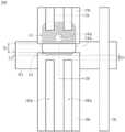
图1A绘示根据本发明一实施例的显示面板100的上视图。图1B绘示图1A的显示面板100沿剖面线1B-1B’的剖视图。如图1A~图1B所示,显示面板100包括一第一基板110、一第一绝缘层120、一共同电极130、一第二绝缘层140、一第一像素电极150以及一第二像素电极160。第一绝缘层120位于第一基板110上。共同电极130位于第一绝缘层120上,且共同电极130具有一第一通孔130a。第二绝缘层140覆盖共同电极130与部分的第一通孔130a。第一像素电极150位于第二绝缘层140上,且第一像素电极150通过第一通孔130a。第二像素电极160位于第二绝缘层140上,且第二像素电极160相邻第一像素电极150。第二像素电极160重叠第一通孔130a的一部分。FIG. 1A illustrates a top view of a
根据本发明的实施例,第二像素电极160相邻第一像素电极150、且第二像素电极160重叠第一通孔130a的一部分,如此一来,可以有效缩短像素电极之间的距离,使得单位面积内可以设置较多数目的像素电极,也就是可以设置较多的像素单元,因而可以有效提升显示面板100的每英寸像素值(ppi)。According to the embodiment of the present invention, the
实施例中,共同电极130全面性地覆盖一个像素单元中的第一绝缘层120以下的结构,仅以第一通孔130a暴露出共同电极130之下的结构。In the embodiment, the
实施例中,第一基板110例如是玻璃基板或塑胶基板,第一绝缘层120例如包括有机绝缘材料。共同电极130、第一像素电极150及第二像素电极160的材质例如可分别包括透明导电材料,例如是铟锡氧化物(ITO)。In an embodiment, the
实施例中,如图1A~图1B所示,第一像素电极150与第二像素电极160相隔一第一距离D1,第二像素电极160向第一通孔130a内延伸一第二距离D2,第一距离D1例如是大于第二距离D2。In the embodiment, as shown in FIGS. 1A-1B , the
由于现今显示面板的每英寸像素值(ppi)渐趋提高的趋势,使得像素单元的尺寸减小,像素电极与共同电极彼此重叠的面积也减少,因而可能产生存储电容减小的疑虑。根据本发明的实施例,如图1B所示,第二像素电极160向第一通孔130a内延伸一第二距离D2,换言之,第二像素电极160完全覆盖共同电极130。再者,如图1B所示,第一像素电极150也完全覆盖共同电极130。根据本发明的第一像素电极150/第二像素电极160和共同电极130的设计,可以使得共同电极130与第一像素电极150/第二像素电极160重叠的面积极大化并夹有第二绝缘层140于其中,如此一来,可以有效提高像素电极与共同电极重叠的面积,进而可以达到提高显示面板的每英寸像素值(ppi)同时也有效提高存储电容。Due to the increasing trend of pixel value per inch (ppi) of the current display panel, the size of the pixel unit is reduced, and the overlapping area of the pixel electrode and the common electrode is also reduced. According to an embodiment of the present invention, as shown in FIG. 1B , the
再者,根据本发明的实施例,第二像素电极160向第一通孔130a内延伸一第二距离D2,也就是说,第二像素电极160延伸并超过共同电极130而覆盖一部分的第一通孔130a,可以有效防止因为制作工艺的误差造成第二像素电极160相对于共同电极130的位置的偏移。换言之,第二像素电极160延伸并超过共同电极130的边缘可以提供制作工艺上的缓冲,使得最终完成的产品可以具有共同电极130与第一像素电极150/第二像素电极160的重叠面积极大化的结构。Furthermore, according to the embodiment of the present invention, the
实施例中,第一距离D1例如是2.0~5.0微米(μm),第二距离例如是0.1~1.0微米。In an embodiment, the first distance D1 is, for example, 2.0-5.0 micrometers (μm), and the second distance is, for example, 0.1-1.0 micrometers.
如图1A所示,实施例中,第二像素电极160可具有至少一狭缝160a,狭缝160a与第一通孔130a相隔一第三距离D3,第三距离D3例如是大于第二距离D2。As shown in FIG. 1A , in the embodiment, the
实施例中,第三距离D3例如是2.0~5.0微米。In the embodiment, the third distance D3 is, for example, 2.0˜5.0 μm.
如图1A所示,实施例中,第一像素电极150与第一通孔130a重叠的一第一面积A1例如是大于第二像素电极160与第一通孔130a重叠的一第二面积A2。As shown in FIG. 1A , in the embodiment, a first area A1 overlapping the
实施例中,显示面板100还可包括一扫描线M1。如图1A~图1B所示,本实施例中,扫描线M1例如是与第二像素电极160的一部分重叠。In an embodiment, the
如图1A所示,实施例中,第一绝缘层140具有一第二通孔140a,第二通孔140a位于第一通孔130a之中,且第二通孔140a例如是小于第一通孔130a。As shown in FIG. 1A, in the embodiment, the first insulating
实施例中,如图1B所示,显示面板100还可包括一金属层M2。第一像素电极150通过第二通孔140a电连接金属层M2。In an embodiment, as shown in FIG. 1B , the
实施例中,第一像素电极150可以经由金属层M2电连接至漏极/源极。In an embodiment, the
实施例中,如图1A所示,显示面板100还可包括一数据线DL。金属层M2可电连接至数据线DL。换言之,第一像素电极150可通过第二通孔140a电连接金属层M2并进而电连接至数据线DL。In an embodiment, as shown in FIG. 1A , the
实施例中,如图1B所示,显示面板100还可包括一第二基板180以及一液晶层170。第一基板110和第二基板180对组,液晶层170位于第一基板110和第二基板180之间。实施例中,第二基板180例如是彩色滤光层基板。In an embodiment, as shown in FIG. 1B , the
实施例中,如图1B所示,显示面板100还可包括一黑色矩阵BM。黑色矩阵BM位于第二基板180上,且对应共同电极130的第一通孔130a。但在其他实施例中,该黑色矩阵BM也可位于第一基板110上,以作为BOA(Black matrix on array)架构。In an embodiment, as shown in FIG. 1B , the
实施例中,如图1B所示,显示面板100还可包括绝缘层181、183、185和187以及半导体层189。扫描线M1位于绝缘层185上,半导体层189位于绝缘层187上。绝缘层181、183、185和187例如可分别包括氮化硅、氧化硅或两者的组合。半导体层189例如可包括多晶硅(polysilicon)、低温多晶硅(LTPS)或非晶相硅(amorphous silicon)。In an embodiment, as shown in FIG. 1B , the
根据本发明的实施例,共同电极130、第一像素电极150和第二像素电极160均位于液晶层170的同一侧,且共同电极130和像素电极150/160之间以第二绝缘层140相隔开来,且此些电极都位于晶体管元件侧的第一基板110之上,显示面板100例如是边缘电场切换型(fringe field switching,FFS)液晶显示面板。According to the embodiment of the present invention, the
图2A绘示根据本发明另一实施例的显示面板200的上视图。图2B绘示图2A的显示面板200沿剖面线2B-2B’的剖视图。本实施例中与前述实施例相同或相似的元件沿用同样或相似的元件标号,且相同或相似元件的相关说明请参考前述,在此不再赘述。FIG. 2A illustrates a top view of a
如图2A~图2B所示,本实施例中,显示面板200的扫描线M1例如是位于第一像素电极150和第二像素电极160之间。扫描线M1并未与第一像素电极150或第二像素电极160重叠。As shown in FIGS. 2A-2B , in this embodiment, the scan line M1 of the
图3A绘示根据本发明再一实施例的显示面板的上视图。图3B绘示图3A的显示面板沿剖面线3B-3B’的剖视图。本实施例中与前述实施例相同或相似的元件沿用同样或相似的元件标号,且相同或相似元件的相关说明请参考前述,在此不再赘述。3A illustrates a top view of a display panel according to yet another embodiment of the present invention. FIG. 3B is a cross-sectional view of the display panel of FIG. 3A along
如图3A~图3B所示,本实施例中,显示面板300的扫描线M1可同时与第一像素电极150的一部分及第二像素电极150的一部分重叠。As shown in FIGS. 3A-3B , in this embodiment, the scan line M1 of the
图4绘示根据本发明又一实施例的显示面板400的上视图。本实施例中与前述实施例相同或相似的元件沿用同样或相似的元件标号,且相同或相似元件的相关说明请参考前述,在此不再赘述。FIG. 4 illustrates a top view of a
如图4所示,显示面板400还可包括一第一晶体管元件190、一第一扫描线M1-1、一第二晶体管元件191及一第二扫描线M1-2。请同时参照图1A~图1B及图4,第一晶体管元件190、第一扫描线M1-1、第二晶体管元件191及第二扫描线M1-2位于第一基板110上。第一晶体管元件190由第一扫描线M1-1所控制,第一晶体管元件190电连接于第一像素电极150。第二晶体管元件191由第二扫描线M1-2所控制,且第二晶体管元件191电连接于第二像素电极160。第二扫描线M1-2相邻第一扫描线M1-1,且第一绝缘层120覆盖第一晶体管元件190与第二晶体管元件191。As shown in FIG. 4, the
虽然结合以上优选实施例公开了本发明,然而其并非用以限定本发明。本发明所属技术领域中具有通常知识者,在不脱离本发明的精神和范围内,可作各种的更动与润饰。因此,本发明的保护范围应当以附上的权利要求所界定的为准。Although the present invention has been disclosed in conjunction with the above preferred embodiments, it is not intended to limit the present invention. Those skilled in the art to which the present invention pertains can make various changes and modifications without departing from the spirit and scope of the present invention. Therefore, the protection scope of the present invention should be defined by the appended claims.
Claims (8)
Translated fromChinesePriority Applications (1)
| Application Number | Priority Date | Filing Date | Title |
|---|---|---|---|
| CN201910661077.6ACN110262149B (en) | 2015-02-12 | 2015-02-12 | display panel |
Applications Claiming Priority (2)
| Application Number | Priority Date | Filing Date | Title |
|---|---|---|---|
| CN201910661077.6ACN110262149B (en) | 2015-02-12 | 2015-02-12 | display panel |
| CN201510074956.0ACN105988250B (en) | 2015-02-12 | 2015-02-12 | Display panel |
Related Parent Applications (1)
| Application Number | Title | Priority Date | Filing Date |
|---|---|---|---|
| CN201510074956.0ADivisionCN105988250B (en) | 2015-02-12 | 2015-02-12 | Display panel |
Publications (2)
| Publication Number | Publication Date |
|---|---|
| CN110262149A CN110262149A (en) | 2019-09-20 |
| CN110262149Btrue CN110262149B (en) | 2022-06-21 |
Family
ID=57041954
Family Applications (2)
| Application Number | Title | Priority Date | Filing Date |
|---|---|---|---|
| CN201910661077.6AActiveCN110262149B (en) | 2015-02-12 | 2015-02-12 | display panel |
| CN201510074956.0AActiveCN105988250B (en) | 2015-02-12 | 2015-02-12 | Display panel |
Family Applications After (1)
| Application Number | Title | Priority Date | Filing Date |
|---|---|---|---|
| CN201510074956.0AActiveCN105988250B (en) | 2015-02-12 | 2015-02-12 | Display panel |
Country Status (1)
| Country | Link |
|---|---|
| CN (2) | CN110262149B (en) |
Citations (4)
| Publication number | Priority date | Publication date | Assignee | Title |
|---|---|---|---|---|
| CN1388405A (en)* | 2001-05-29 | 2003-01-01 | Lg.菲利浦Lcd株式会社 | Method for forming liquid crystal layer with ink jet system |
| CN101441370A (en)* | 2007-11-19 | 2009-05-27 | 株式会社日立显示器 | Liquid crystal display device having a plurality of pixel electrodes |
| CN103018983A (en)* | 2011-09-23 | 2013-04-03 | 三星显示有限公司 | LCD Monitor |
| CN103946742A (en)* | 2011-11-18 | 2014-07-23 | 夏普株式会社 | Semiconductor device, display device, and method for manufacturing semiconductor device |
Family Cites Families (6)
| Publication number | Priority date | Publication date | Assignee | Title |
|---|---|---|---|---|
| JP2007226175A (en)* | 2006-01-26 | 2007-09-06 | Epson Imaging Devices Corp | Liquid crystal device and electronic equipment |
| JP4544251B2 (en)* | 2007-02-27 | 2010-09-15 | ソニー株式会社 | Liquid crystal display element and display device |
| TWI465817B (en)* | 2011-11-23 | 2014-12-21 | Au Optronics Corp | Display panel |
| CN104246593B (en)* | 2012-04-27 | 2016-11-23 | 夏普株式会社 | Liquid crystal display element and liquid crystal display device |
| KR102059371B1 (en)* | 2013-05-24 | 2019-12-27 | 엘지디스플레이 주식회사 | Liquid crystal display device and method for manufacturing the same |
| CN204557027U (en)* | 2015-02-12 | 2015-08-12 | 群创光电股份有限公司 | Display panel |
- 2015
- 2015-02-12CNCN201910661077.6Apatent/CN110262149B/enactiveActive
- 2015-02-12CNCN201510074956.0Apatent/CN105988250B/enactiveActive
Patent Citations (4)
| Publication number | Priority date | Publication date | Assignee | Title |
|---|---|---|---|---|
| CN1388405A (en)* | 2001-05-29 | 2003-01-01 | Lg.菲利浦Lcd株式会社 | Method for forming liquid crystal layer with ink jet system |
| CN101441370A (en)* | 2007-11-19 | 2009-05-27 | 株式会社日立显示器 | Liquid crystal display device having a plurality of pixel electrodes |
| CN103018983A (en)* | 2011-09-23 | 2013-04-03 | 三星显示有限公司 | LCD Monitor |
| CN103946742A (en)* | 2011-11-18 | 2014-07-23 | 夏普株式会社 | Semiconductor device, display device, and method for manufacturing semiconductor device |
Also Published As
| Publication number | Publication date |
|---|---|
| CN105988250B (en) | 2019-08-16 |
| CN105988250A (en) | 2016-10-05 |
| CN110262149A (en) | 2019-09-20 |
Similar Documents
| Publication | Publication Date | Title |
|---|---|---|
| US10371979B2 (en) | Display panel and manufacturing method thereof | |
| CN102394247B (en) | Thin film transistor element, pixel structure of display panel and driving circuit | |
| CN104730782B (en) | Array substrate, display panel and display device | |
| US10579179B2 (en) | Display panel and method for manufacturing the same | |
| CN103926760B (en) | pixel structure and pixel array substrate | |
| CN105404062B (en) | Array substrate and display device | |
| US20160049424A1 (en) | Array substrate and manufacturing method thereof, display device | |
| CN104483790A (en) | Active element array substrate and display panel | |
| CN104201152A (en) | Method for manufacturing display panel | |
| WO2016179904A1 (en) | Array substrate and control display device | |
| CN103488001B (en) | Pixel structure and display panel | |
| CN106449652B (en) | Array substrate and its manufacturing method, display panel and display equipment | |
| CN104317115B (en) | Dot structure and its manufacture method, array base palte, display panel and display device | |
| CN103616785B (en) | Pixel array | |
| CN110764645B (en) | Pixel array substrate | |
| CN104035250A (en) | Active element array substrate | |
| CN101021659A (en) | Liquid crystal pixel, manufacturing method thereof, and liquid crystal display | |
| CN110262149B (en) | display panel | |
| CN204557027U (en) | Display panel | |
| TWI548921B (en) | Display panel | |
| TWI595298B (en) | Display panel | |
| TWI612645B (en) | Display panel | |
| TWI300240B (en) | Systems for providing conducting pad and fabrication method thereof | |
| US7405426B2 (en) | Active device array substrate | |
| CN119126445A (en) | Display device |
Legal Events
| Date | Code | Title | Description |
|---|---|---|---|
| PB01 | Publication | ||
| PB01 | Publication | ||
| SE01 | Entry into force of request for substantive examination | ||
| SE01 | Entry into force of request for substantive examination | ||
| GR01 | Patent grant | ||
| GR01 | Patent grant |