CN110255533B - Method for preparing semiconductor single-walled carbon nanotube based on phenylation modification method, product and application thereof - Google Patents
Method for preparing semiconductor single-walled carbon nanotube based on phenylation modification method, product and application thereofDownload PDFInfo
- Publication number
- CN110255533B CN110255533BCN201910531490.0ACN201910531490ACN110255533BCN 110255533 BCN110255533 BCN 110255533BCN 201910531490 ACN201910531490 ACN 201910531490ACN 110255533 BCN110255533 BCN 110255533B
- Authority
- CN
- China
- Prior art keywords
- walled carbon
- carbon nanotubes
- substrate
- carbon nanotube
- sio
- Prior art date
- Legal status (The legal status is an assumption and is not a legal conclusion. Google has not performed a legal analysis and makes no representation as to the accuracy of the status listed.)
- Active
Links
- 239000002109single walled nanotubeSubstances0.000titleclaimsabstractdescription92
- 238000000034methodMethods0.000titleclaimsabstractdescription30
- 238000005887phenylation reactionMethods0.000titleclaimsabstractdescription20
- 238000002715modification methodMethods0.000titleclaimsabstractdescription9
- 239000004065semiconductorSubstances0.000titleclaimsdescription10
- 239000000758substrateSubstances0.000claimsabstractdescription28
- IJGRMHOSHXDMSA-UHFFFAOYSA-NAtomic nitrogenChemical compoundN#NIJGRMHOSHXDMSA-UHFFFAOYSA-N0.000claimsabstractdescription23
- 229910004298SiO 2Inorganic materials0.000claimsabstractdescription17
- OKTJSMMVPCPJKN-UHFFFAOYSA-NCarbonChemical compound[C]OKTJSMMVPCPJKN-UHFFFAOYSA-N0.000claimsabstractdescription15
- 239000010453quartzSubstances0.000claimsabstractdescription14
- VYPSYNLAJGMNEJ-UHFFFAOYSA-Nsilicon dioxideInorganic materialsO=[Si]=OVYPSYNLAJGMNEJ-UHFFFAOYSA-N0.000claimsabstractdescription14
- 238000005229chemical vapour depositionMethods0.000claimsabstractdescription13
- 239000004342Benzoyl peroxideSubstances0.000claimsabstractdescription6
- OMPJBNCRMGITSC-UHFFFAOYSA-NBenzoylperoxideChemical compoundC=1C=CC=CC=1C(=O)OOC(=O)C1=CC=CC=C1OMPJBNCRMGITSC-UHFFFAOYSA-N0.000claimsabstractdescription6
- KFZMGEQAYNKOFK-UHFFFAOYSA-NIsopropanolChemical compoundCC(C)OKFZMGEQAYNKOFK-UHFFFAOYSA-N0.000claimsabstractdescription6
- 235000019400benzoyl peroxideNutrition0.000claimsabstractdescription6
- 238000001069Raman spectroscopyMethods0.000claimsabstractdescription5
- 238000006243chemical reactionMethods0.000claimsabstractdescription5
- 238000012546transferMethods0.000claimsabstractdescription5
- 230000005669field effectEffects0.000claimsabstractdescription3
- LFQSCWFLJHTTHZ-UHFFFAOYSA-NEthanolChemical compoundCCOLFQSCWFLJHTTHZ-UHFFFAOYSA-N0.000claimsdescription38
- XKRFYHLGVUSROY-UHFFFAOYSA-NArgonChemical compound[Ar]XKRFYHLGVUSROY-UHFFFAOYSA-N0.000claimsdescription32
- CSCPPACGZOOCGX-UHFFFAOYSA-NAcetoneChemical compoundCC(C)=OCSCPPACGZOOCGX-UHFFFAOYSA-N0.000claimsdescription16
- 229910052786argonInorganic materials0.000claimsdescription16
- 229910021642ultra pure waterInorganic materials0.000claimsdescription14
- 239000012498ultrapure waterSubstances0.000claimsdescription14
- 229910052757nitrogenInorganic materials0.000claimsdescription10
- 229910052799carbonInorganic materials0.000claimsdescription8
- 238000004140cleaningMethods0.000claimsdescription7
- 239000001257hydrogenSubstances0.000claimsdescription7
- 229910052739hydrogenInorganic materials0.000claimsdescription7
- 239000003054catalystSubstances0.000claimsdescription6
- 239000000203mixtureSubstances0.000claimsdescription6
- QVGXLLKOCUKJST-UHFFFAOYSA-Natomic oxygenChemical compound[O]QVGXLLKOCUKJST-UHFFFAOYSA-N0.000claimsdescription4
- 239000012159carrier gasSubstances0.000claimsdescription4
- 238000001816coolingMethods0.000claimsdescription4
- 238000001035dryingMethods0.000claimsdescription4
- 229910052742ironInorganic materials0.000claimsdescription4
- 239000001301oxygenSubstances0.000claimsdescription4
- 229910052760oxygenInorganic materials0.000claimsdescription4
- 238000002791soakingMethods0.000claimsdescription4
- 238000010276constructionMethods0.000claimsdescription2
- 125000004435hydrogen atomChemical class[H]*0.000claimsdescription2
- 125000001997phenyl groupChemical group[H]C1=C([H])C([H])=C(*)C([H])=C1[H]0.000claimsdescription2
- PNEYBMLMFCGWSK-UHFFFAOYSA-NAluminaChemical compound[O-2].[O-2].[O-2].[Al+3].[Al+3]PNEYBMLMFCGWSK-UHFFFAOYSA-N0.000claims2
- CPLXHLVBOLITMK-UHFFFAOYSA-NMagnesium oxideChemical compound[Mg]=OCPLXHLVBOLITMK-UHFFFAOYSA-N0.000claims2
- 230000001678irradiating effectEffects0.000claims2
- 238000000861blow dryingMethods0.000claims1
- 238000007664blowingMethods0.000claims1
- 238000010438heat treatmentMethods0.000claims1
- 239000000395magnesium oxideSubstances0.000claims1
- 238000002203pretreatmentMethods0.000claims1
- 238000004506ultrasonic cleaningMethods0.000claims1
- 229910001873dinitrogenInorganic materials0.000abstractdescription3
- 238000002360preparation methodMethods0.000abstractdescription3
- 238000011160researchMethods0.000abstractdescription3
- 238000000926separation methodMethods0.000abstract1
- XEEYBQQBJWHFJM-UHFFFAOYSA-NIronChemical compound[Fe]XEEYBQQBJWHFJM-UHFFFAOYSA-N0.000description9
- 238000005991sulfenylation reactionMethods0.000description8
- UFHFLCQGNIYNRP-UHFFFAOYSA-NHydrogenChemical compound[H][H]UFHFLCQGNIYNRP-UHFFFAOYSA-N0.000description7
- 239000007789gasSubstances0.000description7
- 238000000137annealingMethods0.000description6
- 239000010408filmSubstances0.000description6
- 238000001878scanning electron micrographMethods0.000description6
- 238000001237Raman spectrumMethods0.000description4
- 238000003491arrayMethods0.000description4
- 239000002041carbon nanotubeSubstances0.000description4
- 229910021393carbon nanotubeInorganic materials0.000description4
- 229920003229poly(methyl methacrylate)Polymers0.000description4
- 239000004926polymethyl methacrylateSubstances0.000description4
- 239000010409thin filmSubstances0.000description3
- PXHVJJICTQNCMI-UHFFFAOYSA-NNickelChemical compound[Ni]PXHVJJICTQNCMI-UHFFFAOYSA-N0.000description2
- 239000000853adhesiveSubstances0.000description2
- 230000001070adhesive effectEffects0.000description2
- 230000005587bubblingEffects0.000description2
- 238000000609electron-beam lithographyMethods0.000description2
- 239000000463materialSubstances0.000description2
- 239000002184metalSubstances0.000description2
- 229910052751metalInorganic materials0.000description2
- 230000004048modificationEffects0.000description2
- 238000012986modificationMethods0.000description2
- 238000012360testing methodMethods0.000description2
- RYGMFSIKBFXOCR-UHFFFAOYSA-NCopperChemical compound[Cu]RYGMFSIKBFXOCR-UHFFFAOYSA-N0.000description1
- XUIMIQQOPSSXEZ-UHFFFAOYSA-NSiliconChemical compound[Si]XUIMIQQOPSSXEZ-UHFFFAOYSA-N0.000description1
- XTUNVEMVWFXFGV-UHFFFAOYSA-N[C].CCOChemical compound[C].CCOXTUNVEMVWFXFGV-UHFFFAOYSA-N0.000description1
- 229910017052cobaltInorganic materials0.000description1
- 239000010941cobaltSubstances0.000description1
- GUTLYIVDDKVIGB-UHFFFAOYSA-Ncobalt atomChemical compound[Co]GUTLYIVDDKVIGB-UHFFFAOYSA-N0.000description1
- 230000000295complement effectEffects0.000description1
- 239000002131composite materialSubstances0.000description1
- 229910052802copperInorganic materials0.000description1
- 239000010949copperSubstances0.000description1
- 230000007547defectEffects0.000description1
- 238000010586diagramMethods0.000description1
- 230000000694effectsEffects0.000description1
- 238000005516engineering processMethods0.000description1
- 125000000219ethylidene groupChemical group[H]C(=[*])C([H])([H])[H]0.000description1
- 239000007788liquidSubstances0.000description1
- 229910044991metal oxideInorganic materials0.000description1
- 150000004706metal oxidesChemical class0.000description1
- VNWKTOKETHGBQD-UHFFFAOYSA-NmethaneChemical compoundCVNWKTOKETHGBQD-UHFFFAOYSA-N0.000description1
- 239000002086nanomaterialSubstances0.000description1
- 229910052759nickelInorganic materials0.000description1
- 230000003287optical effectEffects0.000description1
- 239000002245particleSubstances0.000description1
- 230000000704physical effectEffects0.000description1
- 230000008569processEffects0.000description1
- 230000009257reactivityEffects0.000description1
- 230000008439repair processEffects0.000description1
- 239000000523sampleSubstances0.000description1
- 229910052710siliconInorganic materials0.000description1
- 239000010703siliconSubstances0.000description1
Images


Classifications
- C—CHEMISTRY; METALLURGY
- C01—INORGANIC CHEMISTRY
- C01B—NON-METALLIC ELEMENTS; COMPOUNDS THEREOF; METALLOIDS OR COMPOUNDS THEREOF NOT COVERED BY SUBCLASS C01C
- C01B32/00—Carbon; Compounds thereof
- C01B32/15—Nano-sized carbon materials
- C01B32/158—Carbon nanotubes
- C01B32/159—Carbon nanotubes single-walled
- C—CHEMISTRY; METALLURGY
- C01—INORGANIC CHEMISTRY
- C01B—NON-METALLIC ELEMENTS; COMPOUNDS THEREOF; METALLOIDS OR COMPOUNDS THEREOF NOT COVERED BY SUBCLASS C01C
- C01B32/00—Carbon; Compounds thereof
- C01B32/15—Nano-sized carbon materials
- C01B32/158—Carbon nanotubes
- C01B32/16—Preparation
- C—CHEMISTRY; METALLURGY
- C01—INORGANIC CHEMISTRY
- C01B—NON-METALLIC ELEMENTS; COMPOUNDS THEREOF; METALLOIDS OR COMPOUNDS THEREOF NOT COVERED BY SUBCLASS C01C
- C01B32/00—Carbon; Compounds thereof
- C01B32/15—Nano-sized carbon materials
- C01B32/158—Carbon nanotubes
- C01B32/168—After-treatment
- C01B32/174—Derivatisation; Solubilisation; Dispersion in solvents
- C—CHEMISTRY; METALLURGY
- C01—INORGANIC CHEMISTRY
- C01B—NON-METALLIC ELEMENTS; COMPOUNDS THEREOF; METALLOIDS OR COMPOUNDS THEREOF NOT COVERED BY SUBCLASS C01C
- C01B2202/00—Structure or properties of carbon nanotubes
- C01B2202/02—Single-walled nanotubes
Landscapes
- Chemical & Material Sciences (AREA)
- Engineering & Computer Science (AREA)
- Materials Engineering (AREA)
- Nanotechnology (AREA)
- Organic Chemistry (AREA)
- Inorganic Chemistry (AREA)
- Carbon And Carbon Compounds (AREA)
Abstract
Translated fromChinese
Description
Translated fromChinese技术领域technical field
本发明涉及微纳米材料制备技术领域,具体涉及半导体性单壁碳纳米管,特别是指基于苯基化修饰方法制备半导体性单壁碳纳米管的方法及其制品和应用。The invention relates to the technical field of preparation of micro-nano materials, in particular to semiconducting single-walled carbon nanotubes, in particular to a method for preparing semiconducting single-walled carbon nanotubes based on a phenylation modification method, as well as products and applications thereof.
背景技术Background technique
单壁碳纳米管具有完美的共轭结构和优异的物理性能,自1991年被日本科学家Iijima发现以来,便成为纳米科学领域中研究的热点之一。由于单壁碳纳米管优异的电学、光学及力学等性能使其在纳电子器件、能源转换、生物传感及复合材料等诸多领域具有广阔的应用前景。尤其在纳电子学领域,许多研究表明,硅基CMOS(互补金属氧化物半导体,Complementary Metal Oxide Semiconductor)技术在2020年左右将达到其极限,在为数不多的替代材料中,碳纳米管是唯一可以通过减小器件直至5纳米节点而继续提高系统整体性能的材料。但是通常合成的单壁碳纳米管是半导体性单壁碳纳米管和金属性单壁碳纳米管的混合物,其中约含有1/3的金属性单壁碳纳米管。由于只有半导体性单壁碳纳米管对器件的构建有贡献,金属性单壁碳纳米管的存在会大大降低这些器件的性能,因此获得能用来构建高密度单壁碳纳米管器件的半导体性单壁碳纳米管阵列,对半导体性单壁碳纳米管性质及其器件性能研究具有非常重要的价值和意义。Single-walled carbon nanotubes have a perfect conjugated structure and excellent physical properties. Since they were discovered by Japanese scientist Iijima in 1991, they have become one of the research hotspots in the field of nanoscience. Due to the excellent electrical, optical, and mechanical properties of single-walled carbon nanotubes, they have broad application prospects in many fields such as nanoelectronic devices, energy conversion, biosensing, and composite materials. Especially in the field of nanoelectronics, many studies have shown that silicon-based CMOS (Complementary Metal Oxide Semiconductor) technology will reach its limit around 2020. Among the few alternative materials, carbon nanotubes are the only ones. Materials that can continue to improve overall system performance by shrinking devices down to the 5nm node. However, the generally synthesized single-walled carbon nanotubes are a mixture of semiconducting single-walled carbon nanotubes and metallic single-walled carbon nanotubes, which contain about 1/3 of metallic single-walled carbon nanotubes. Since only semiconducting single-walled carbon nanotubes contribute to the construction of devices, the presence of metallic single-walled carbon nanotubes will greatly reduce the performance of these devices, so the semiconducting properties that can be used to build high-density single-walled carbon nanotube devices Single-walled carbon nanotube arrays are of great value and significance to the research on the properties of semiconducting single-walled carbon nanotubes and their device performance.
发明内容Contents of the invention
本发明实施例所要解决的技术问题在于,提供一种基于苯基化修饰方法制备半导体性单壁碳纳米管的方法。该方法利用了过氧化苯甲酰在拉曼激光的照射下产生苯基并与单壁碳纳米管发生反应。由于金属/半导体性单壁碳纳米管反应活性的差异,我们可以选择性的与金属性单壁碳纳米管进行苯基化反应,使其转变为半导体管,从而使整体的单壁碳纳米管呈现半导体性能。The technical problem to be solved by the embodiments of the present invention is to provide a method for preparing semiconducting single-walled carbon nanotubes based on a phenylation modification method. The method uses benzoyl peroxide to generate phenyl groups under the irradiation of Raman laser and react with single-walled carbon nanotubes. Due to the difference in reactivity of metal/semiconductor single-walled carbon nanotubes, we can selectively carry out phenylation reaction with metallic single-walled carbon nanotubes to transform them into semiconductor tubes, so that the overall single-walled carbon nanotubes Exhibits semiconductor properties.
为实现上述目的,本发明的技术方案是发明所提供一种制备半导体性单壁碳纳米管的方法,包括:In order to achieve the above object, the technical solution of the present invention is a method for preparing semiconducting single-walled carbon nanotubes provided by the invention, comprising:
步骤S1利用化学气相沉积(CVD)在ST-cut石英上生长单壁碳纳米管;Step S1 utilizes chemical vapor deposition (CVD) to grow single-walled carbon nanotubes on ST-cut quartz;
步骤S2将步骤S1在ST-cut石英中生长的单壁碳纳米管转移到SiO2/Si基底上;Step S2 transfers the single-walled carbon nanotubes grown in ST-cut quartz in step S1 to the SiO2 /Si substrate;
步骤S3将步骤S2中的SiO2/Si基底浸泡在过氧化苯甲酰溶液中,取出并用氮气吹干,然后用532nm拉曼激光照射使之反应,最后用乙醇清洗并用氮气吹干;In step S3, soak the SiO2 /Si substrate in step S2 in a benzoyl peroxide solution, take it out and dry it with nitrogen, then irradiate it with a 532nm Raman laser to make it react, and finally wash it with ethanol and dry it with nitrogen;
步骤S1包括如下步骤:Step S1 comprises the following steps:
在生长单壁碳纳米管之前,将所述ST-cut石英进行预处理;Before growing single-walled carbon nanotubes, the ST-cut quartz is pretreated;
ST-cut石英预处理:超纯水、丙酮、乙醇和超纯水中各超声清洗20min,氮气吹干后,在3h内由室温升至1100℃后恒温8h,再在15h内降温至300℃,再自然降温至室温;ST-cut quartz pretreatment: ultrapure water, acetone, ethanol, and ultrapure water were ultrasonically cleaned for 20 minutes, dried with nitrogen, then raised from room temperature to 1100°C within 3 hours, then kept at a constant temperature for 8 hours, and then cooled to 300°C within 15 hours °C, and then cooled down to room temperature naturally;
铁、钴、镍、铜作为生长单壁碳纳米管的催化剂,在这里优先选用铁。铁/乙醇溶液的含量为0.01-0.1mmol/L,优选0.05mmol/L;Iron, cobalt, nickel, and copper are used as catalysts for growing single-walled carbon nanotubes, and iron is preferred here. The content of iron/ethanol solution is 0.01-0.1mmol/L, preferably 0.05mmol/L;
所述化学气相沉积步骤方法中,碳源是含碳气体或蒸汽压较大并易裂解的含碳液体,具体可为C2H4、乙醇、CH4或异丙醇,在这里优先选用乙醇,乙醇碳源是通过氩气鼓泡乙醇溶液产生的;In the chemical vapor deposition step method, the carbon source is a carbon-containing gas or a carbon- containing liquid with a relatively large vapor pressure and is easily cracked, specificallyC2H4 , ethanol,CH4 or isopropanol, and ethanol is preferred here , the ethanol carbon source is produced by bubbling the ethanol solution with argon;
碳源的气体流量为10sccm-500sccm,在这里优先选用35sccm;The gas flow rate of the carbon source is 10sccm-500sccm, and 35sccm is preferred here;
还原气氛均为氢气气氛;氢气的气体流量为30-500sccm,在这里优先选用300sccm;The reducing atmosphere is hydrogen atmosphere; the gas flow rate of hydrogen is 30-500sccm, and 300sccm is preferred here;
还原气氛所用载气均为氩气;所述载气的气流流量为50-500sccm,在这里优先选用300sccm;The carrier gas used in the reducing atmosphere is argon; the flow rate of the carrier gas is 50-500 sccm, preferably 300 sccm here;
生长温度均为600℃-900℃,具体为840℃,生长时间均为1min~1h,具体为30min;The growth temperature is 600°C-900°C, specifically 840°C, and the growth time is 1min-1h, specifically 30min;
步骤S1还包括如下步骤:在所述化学气相沉积步骤之后,将体系降温;所述降温具体为自然降温或程序控制降温。Step S1 also includes the following step: after the chemical vapor deposition step, lowering the temperature of the system; specifically, the lowering of temperature is natural cooling or program-controlled cooling.
步骤S2包括如下步骤:Step S2 comprises the following steps:
在转移单壁碳纳米管之前,将所述SiO2/Si基底进行预处理;Before transferring the single-walled carbon nanotubes, pretreating the SiO2 /Si substrate;
SiO2/Si基底在超纯水、丙酮、乙醇和超纯水中各超声清洗20min,氮气吹干后,用氧等离子体清洗系统清洗5-20min,优选15min;SiO2 /Si substrates were ultrasonically cleaned in ultrapure water, acetone, ethanol, and ultrapure water for 20 minutes, and then dried with nitrogen gas, then cleaned with an oxygen plasma cleaning system for 5-20 minutes, preferably 15 minutes;
利用匀胶机在ST-cut石英上涂上PMMA,旋涂时间为20-60s,优选40s,并烘干,时间为1-5min,优选3min;Coat PMMA on the ST-cut quartz with a coater for 20-60s, preferably 40s, and dry for 1-5min, preferably 3min;
利用HF作为转移的溶液,HF溶液质量浓度为1%-10%,优选5%;Using HF as the transferred solution, the mass concentration of HF solution is 1%-10%, preferably 5%;
转移到SiO2/Si基底上PMMA薄膜(粘着单壁碳纳米管)通过热台烘干,烘干时间为1h-4h,优选2h;Transfer to the PMMA film (adhesive single-walled carbon nanotubes) on the SiO2 /Si substrate and dry it on a hot table. The drying time is 1h-4h, preferably 2h;
SiO2/Si基底上PMMA薄膜(粘着单壁碳纳米管)浸泡在丙酮中,去除PMMA,浸泡时间为1min-10min,优选5min;Soak the PMMA film (adhesive single-walled carbon nanotubes) on the SiO2 /Si substrate in acetone to remove the PMMA. The soaking time is 1min-10min, preferably 5min;
步骤S3包括如下步骤:Step S3 comprises the following steps:
将上述SiO2/Si基底浸泡在过氧化苯甲酰溶液中,溶液浓度为0.1mmol/L-1mmol/L,优选0.5mmol/L,浸泡时间为10min-60min,优选30min,532nm激光功率为0.5mW-5mW,优选2mW,照射时间为10s-2min,优选1min;Soak the above SiO2 /Si substrate in benzoyl peroxide solution, the concentration of the solution is 0.1mmol/L-1mmol/L, preferably 0.5mmol/L, the soaking time is 10min-60min, preferably 30min, and the laser power of 532nm is 0.5 mW-5mW, preferably 2mW, the irradiation time is 10s-2min, preferably 1min;
本发明所制备的苯基化修饰的半导体性单壁碳纳米管包括如下步骤:The semiconducting single-walled carbon nanotubes modified by phenylation prepared by the present invention comprise the following steps:
利用电子束光刻技术(EBL)在SiO2/Si基底上定位并蒸镀Cr/Au来制备单壁碳纳米管的FET器件,Cr的厚度为1-5nm,优选3nm,Au的厚度为30-80nm,优选60nm。Using electron beam lithography (EBL) to position and vapor-deposit Cr/Au on SiO2 /Si substrates to prepare single-walled carbon nanotube FET devices, the thickness of Cr is 1-5nm, preferably 3nm, and the thickness of Au is 30 -80nm, preferably 60nm.
利用探针台对制备的FET器件进行电学测试,结果表明此方法制备出的半导体性单壁碳纳米管纯度高于90%。The electrical test of the prepared FET device is carried out by using a probe station, and the result shows that the purity of the semiconducting single-wall carbon nanotube prepared by this method is higher than 90%.
单壁碳纳米管苯基化是一种新型的碳管“分离”方法,区别于传统的方法,此方法选择不去除金属管,而只使其呈现半导体性能,从而使整体的单壁碳纳米管呈现半导体性,本发明具体效果可见本发明实施例实验数据。Single-walled carbon nanotube sulfenation is a new method of "separating" carbon tubes. Different from traditional methods, this method does not remove metal tubes, but only makes them exhibit semiconductor properties, so that the overall single-walled carbon nanotubes The tube exhibits semiconductor properties, and the specific effects of the present invention can be seen from the experimental data of the embodiments of the present invention.
附图说明Description of drawings
为了更清楚地说明本发明实施例或现有技术中的技术方案,下面将对实施例或现有技术描述中所需要使用的附图作简单地介绍,显而易见地,下面描述中的附图仅仅是本发明的一些实施例,对于本领域普通技术人员来讲,在不付出创造性劳动性的前提下,根据这些附图获得其他的附图仍属于本发明的范畴。In order to more clearly illustrate the technical solutions in the embodiments of the present invention or the prior art, the following will briefly introduce the drawings that need to be used in the description of the embodiments or the prior art. Obviously, the accompanying drawings in the following description are only These are some embodiments of the present invention. For those of ordinary skill in the art, obtaining other drawings based on these drawings still belongs to the scope of the present invention without any creative effort.
图1单壁碳纳米管示苯基化示意图;Figure 1 shows a schematic diagram of phenylation of single-walled carbon nanotubes;
图2其中,(图2a,图2b)单根的单壁碳纳米管FET器件SEM图像,(图2c)在Vds=1V时单根的单壁碳纳米管苯基化前后典型Ids-Vg曲线,(图2d,图2e)单壁碳纳米管水平阵列FET器件SEM图像,(图2f)在Vds=1V时单壁碳纳米管水平阵列苯基化前后典型Ids-Vg曲线,(图2g,图2h)单壁碳纳米管薄膜FET器件SEM图像,(图2i)在Vds=1V时单壁碳纳米管薄膜苯基化前后典型Ids-Vg曲线;Fig. 2 Among them, (Fig. 2a, Fig. 2b) SEM image of a single single-walled carbon nanotube FET device, (Fig. 2c) the typical Ids of a single single-walled carbon nanotube before and after phenylation at Vds = 1V - Vg curves, (Fig. 2d, Fig. 2e) SEM images of single-walled carbon nanotube horizontal array FET devices, (Fig. 2f) typical Ids -Vg of single-walled carbon nanotube horizontal array before and after sulfenylation at Vds = 1V Curves, (Fig. 2g, Fig. 2h) SEM images of single-walled carbon nanotube thin film FET devices, (Fig. 2i) typical Ids -Vg curves of single-walled carbon nanotube thin films before and after phenylation at Vds = 1V;
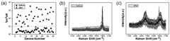
图3其中(图3a)单壁碳纳米管水平阵列苯基化前后Ion/Ioff比率统计,(图3b,图3c)单壁碳纳米管苯基化前后拉曼光谱;Fig. 3 wherein (Fig. 3a) Ion/Ioff ratio statistics of single-walled carbon nanotube horizontal arrays before and aftersulphonation , (Fig. 3b, Fig. 3c) Raman spectrum of single-walled carbon nanotubes before and after sulphonation;
图4其中(图4a)单壁碳纳米管苯基化前、苯基化后以及退火后典型Ids-Vg曲线,(图4b,图4c,图4d)单壁碳纳米管苯基化前、苯基化后以及退火后拉曼光谱。Figure 4 where (Figure 4a) the typical Ids -Vg curves of SWNTs before, after sulfenylation and after annealing, (Figure 4b, Figure 4c, Figure 4d) the sulfenation of SWNTs Raman spectra before, after sulfenylation and after annealing.
具体实施方式detailed description
为使本发明的目的、技术方案和优点更加清楚,下面将结合附图对本发明作进一步地详细描述。In order to make the object, technical solution and advantages of the present invention clearer, the present invention will be further described in detail below in conjunction with the accompanying drawings.
实施例1Example 1
单根的单壁碳纳米管苯基化修饰Sulfenylation of Single Single-Walled Carbon Nanotubes
(1)选用SiO2/Si基底作为碳纳米管生长的基底,依次在超纯水、丙酮、乙醇和超纯水中各超声清洗20min,氮气吹干后,用氧等离子体清洗系统清洗15min;(1) Select the SiO2 /Si substrate as the substrate for the growth of carbon nanotubes, ultrasonically clean them in ultrapure water, acetone, ethanol and ultrapure water for 20 minutes, and dry them with nitrogen, then clean them with an oxygen plasma cleaning system for 15 minutes;
(2)在SiO2/Si基底的一边负载上催化剂Fe然后置入化学气相沉积系统内,催化剂条带垂直于气流方向,升温到950℃,通入300sccm氩气5min,300sccm氢气,最后用35sccm氩气鼓泡乙醇,生长30min,生长完成后,关闭鼓乙醇用的氩气,保持氢气和其余氩气继续通入,自然降至室温,至此气流定向单壁碳纳米管生长结束。(2) Load the catalyst Fe on one side of the SiO2 /Si substrate and then put it into the chemical vapor deposition system. The catalyst strip is perpendicular to the direction of the gas flow, and the temperature is raised to 950 ° C. 300 sccm argon gas is introduced for 5 minutes, 300 sccm hydrogen gas is used, and finally 35 sccm is used. Ethanol was bubbled with argon, and grown for 30 minutes. After the growth was completed, the argon used for ethanol bubbling was turned off, and hydrogen and other argon were kept flowing in, and the temperature was naturally lowered to room temperature. At this point, the growth of airflow-oriented single-walled carbon nanotubes was completed.
图2a,2b是单根单壁碳纳米管FET器件的SEM图像,图2c是在Vds=1V时单根单壁碳纳米管苯基化前后典型Ids-Vg曲线,结果显示金属性单壁碳纳米管苯基化后变为具有半导体性能的单壁碳纳米管。Figures 2a and 2b are SEM images of a single single-walled carbon nanotube FET device, and Figure 2c is a typical Ids -Vg curve of a single single-walled carbon nanotube before and after phenylation at Vds = 1V, and the results show metallicity Single-walled carbon nanotubes become single-walled carbon nanotubes with semiconductor properties after phenylation.
实施例2Example 2
单壁碳纳米管水平阵列苯基化修饰Sulfenylation Modification of Horizontal Arrays of Single-walled Carbon Nanotubes
(1)选用ST-cut石英基底作为碳纳米管生长的基底,依次在超纯水、丙酮、乙醇和超纯水中各超声清洗20min,再用高纯氮气吹干。将清洗干净的基底放入马弗炉中,空气中高温退火,3h升到900℃,在900℃恒温8h,再15h降温至300℃,自然降温冷却,此过程用来修复由于生产加工过程中产生的晶格缺陷。(1) The ST-cut quartz substrate was selected as the substrate for the growth of carbon nanotubes, ultrasonically cleaned in ultrapure water, acetone, ethanol and ultrapure water for 20 min each, and then dried with high-purity nitrogen. Put the cleaned substrate into a muffle furnace, anneal at high temperature in the air, raise it to 900°C for 3 hours, keep the temperature at 900°C for 8 hours, then cool it down to 300°C for 15 hours, and cool it down naturally. This process is used to repair the resulting lattice defects.
(2)在ST-cut石英负载上催化剂Fe然后置入化学气相沉积系统内,升温到840℃,通入300sccm氩气5min,300sccm氢气,最后用35sccm氩气鼓泡乙醇,生长30min,生长完成后,关闭鼓乙醇用的氩气,保持氢气和其余氩气继续通入,自然降至室温。(2) Catalyst Fe is loaded on ST-cut quartz and placed in a chemical vapor deposition system, the temperature is raised to 840°C, 300 sccm argon is introduced for 5 minutes, 300 sccm hydrogen is introduced, and finally ethanol is bubbled with 35 sccm argon, and the growth is completed for 30 minutes. Finally, turn off the argon used to drum ethanol, keep the hydrogen and the rest of the argon flowing in, and let it drop to room temperature naturally.
(3)将ST-cut石英上的单壁碳纳米管转移至SiO2/Si基底上,构筑场效应晶体管,进行电学性能测试。图2d,3e是单壁碳纳米管水平阵列FET器件的SEM图像,图2f是在Vds=1V时单壁碳纳米管水平阵列苯基化前后的典型Ids-Vg曲线,结果显示单壁碳纳米管苯基化后呈现半导体性能。图3a是单壁碳纳米管阵列苯基化前后Ion/Ioff比率统计,表明此苯基化方法制备出纯度90%以上的半导体性单壁碳纳米管水平阵列。图3b,3c是单壁碳纳米管苯基化前后拉曼光谱,苯基化前单壁碳纳米管无D峰,证明反应前单壁碳纳米管是无缺陷的。而反应后出现D峰,D/G比较强,说明单壁碳纳米管实现了苯基化;(3) Transfer the single-walled carbon nanotubes on the ST-cut quartz to the SiO2 /Si substrate to construct a field effect transistor for electrical performance testing. Figure 2d, 3e are SEM images of single-walled carbon nanotube horizontal array FET devices, and Figure 2f is a typical Ids -Vg curve of single-walled carbon nanotube horizontal array before and after phenylation at Vds = 1V, the results show that single Walled carbon nanotubes exhibit semiconducting properties after phenylation. Figure 3a is the statistics of Ion /Ioff ratio before and after sulphonation of single-walled carbon nanotube arrays, indicating that this sulphonation method produces a horizontal array of semiconducting single-walled carbon nanotubes with a purity of more than 90%. Figures 3b and 3c are the Raman spectra of the single-walled carbon nanotubes before and after sulfenylation, and there is no D peak of the single-walled carbon nanotubes before sulfenylation, which proves that the single-walled carbon nanotubes are defect-free before the reaction. After the reaction, the D peak appears, and the D/G is relatively strong, indicating that the single-walled carbon nanotubes have been phenylated;
实施例3Example 3
单壁碳纳米管薄膜苯基化修饰Shenylation Modification of Single-walled Carbon Nanotube Thin Films
(1)选用SiO2/Si基底作为碳纳米管生长的基底,依次在超纯水、丙酮、乙醇和超纯水中各超声清洗20min,氮气吹干后,用氧等粒子清洗系统清洗15min;(1) Select the SiO2 /Si substrate as the substrate for the growth of carbon nanotubes, ultrasonically clean in ultrapure water, acetone, ethanol, and ultrapure water for 20 minutes, and then dry with nitrogen for 15 minutes with a particle cleaning system such as oxygen;
(2)在SiO2/Si基底的负载上催化剂Fe然后置入化学气相沉积系统内,升温到840℃,通入300sccm氩气5min,300sccm氢气,最后用35sccm氩气鼓泡乙醇,生长30min,生长完成后,关闭鼓乙醇用的氩气,保持氢气和其余氩气继续通入,自然降至室温。(2) Catalyst Fe is placed on the SiO2 /Si substrate and then placed in a chemical vapor deposition system, the temperature is raised to 840° C., 300 sccm argon gas is passed through for 5 minutes, 300 sccm hydrogen gas is introduced, and ethanol is finally bubbled with 35 sccm argon gas to grow for 30 minutes. After the growth is completed, close the argon used to drum ethanol, keep the hydrogen and the rest of the argon flowing in, and cool down to room temperature naturally.
图2g,3h是单壁碳纳米管薄膜FET器件的SEM图像,图2i是在Vds=1V时单壁碳纳米管薄膜苯基化前后典型Ids-Vg曲线,显示单壁碳纳米管薄膜苯基化后变为具有半导体性能的单壁碳纳米管薄膜。Figures 2g and 3h are SEM images of single-walled carbon nanotube film FET devices, and Figure 2i is a typical Ids -Vg curve of single-walled carbon nanotube film before and after phenylation at Vds = 1V, showing that single-walled carbon nanotubes After the film is phenylated, it becomes a single-walled carbon nanotube film with semiconducting properties.
将苯基化后的单壁碳纳米管进行退火处理,图4a是单壁碳纳米管苯基化前、苯基化后以及退火后典型Ids-Vg曲线,从图中我们发现退火后单壁碳纳米管恢复到原来的性质。图4b,4c,4d是苯基化前、苯基化后以及退火后拉曼光谱,从图中我们发现退火后D峰消失,单壁碳纳米管又恢复原状。Anneal the phenylated SWNTs. Figure 4a shows the typical Ids -Vg curves of SWNTs before, after, and after annealing. From the figure, we find that after annealing The single-walled carbon nanotubes return to their original properties. Figures 4b, 4c, and 4d are the Raman spectra before sulfenylation, after phenylation, and after annealing. From the figures, we found that the D peak disappeared after annealing, and the single-walled carbon nanotubes returned to their original shape.
以上所揭露的仅为本发明较佳实施例而已,当然不能以此来限定本发明之权利范围,因此依本发明权利要求所作的等同变化,仍属本发明所涵盖的范围。The above disclosures are only preferred embodiments of the present invention, and certainly cannot limit the scope of rights of the present invention. Therefore, equivalent changes made according to the claims of the present invention still fall within the scope of the present invention.
Claims (9)
Priority Applications (1)
| Application Number | Priority Date | Filing Date | Title |
|---|---|---|---|
| CN201910531490.0ACN110255533B (en) | 2019-06-19 | 2019-06-19 | Method for preparing semiconductor single-walled carbon nanotube based on phenylation modification method, product and application thereof |
Applications Claiming Priority (1)
| Application Number | Priority Date | Filing Date | Title |
|---|---|---|---|
| CN201910531490.0ACN110255533B (en) | 2019-06-19 | 2019-06-19 | Method for preparing semiconductor single-walled carbon nanotube based on phenylation modification method, product and application thereof |
Publications (2)
| Publication Number | Publication Date |
|---|---|
| CN110255533A CN110255533A (en) | 2019-09-20 |
| CN110255533Btrue CN110255533B (en) | 2022-12-27 |
Family
ID=67919386
Family Applications (1)
| Application Number | Title | Priority Date | Filing Date |
|---|---|---|---|
| CN201910531490.0AActiveCN110255533B (en) | 2019-06-19 | 2019-06-19 | Method for preparing semiconductor single-walled carbon nanotube based on phenylation modification method, product and application thereof |
Country Status (1)
| Country | Link |
|---|---|
| CN (1) | CN110255533B (en) |
Families Citing this family (1)
| Publication number | Priority date | Publication date | Assignee | Title |
|---|---|---|---|---|
| CN113328038B (en)* | 2021-04-21 | 2022-08-30 | 温州大学 | Preparation method of graphene-carbon nanotube heterojunction |
Family Cites Families (1)
| Publication number | Priority date | Publication date | Assignee | Title |
|---|---|---|---|---|
| US9416009B2 (en)* | 2009-06-26 | 2016-08-16 | Nanyang Technological University | Method for modifying electrical properties of carbon nanotubes |
- 2019
- 2019-06-19CNCN201910531490.0Apatent/CN110255533B/enactiveActive
Also Published As
| Publication number | Publication date |
|---|---|
| CN110255533A (en) | 2019-09-20 |
Similar Documents
| Publication | Publication Date | Title |
|---|---|---|
| US6350488B1 (en) | Mass synthesis method of high purity carbon nanotubes vertically aligned over large-size substrate using thermal chemical vapor deposition | |
| CN111943171B (en) | Controllable preparation method of high-density single-walled carbon nanotube horizontal array | |
| CN113035942B (en) | Molybdenum disulfide/molybdenum diselenide vertical heterojunction and preparation method thereof | |
| CN103011130B (en) | The method of hydrogen in-situ weak etching growing high-quality semi-conductive single-walled carbon nanotubes | |
| CN109850873B (en) | Preparation method of single-walled carbon nanotube intramolecular junction | |
| CN105800602A (en) | Method for directly growing graphene on insulating substrate through remote catalysis of copper particle | |
| CN103332675B (en) | Based on the method for graphene quantum dot chemical vapour deposition synthesizing carbon nanotubes | |
| CN110255533B (en) | Method for preparing semiconductor single-walled carbon nanotube based on phenylation modification method, product and application thereof | |
| CN108910868B (en) | Method for preparing graphene dendrite on insulating substrate | |
| CN109678138B (en) | Preparation method of single-chiral single-walled carbon nanotube | |
| CN104124122B (en) | Method for improving carbon nanotube field emitting performance through diamond-like carbon film | |
| CN116102003B (en) | Dry method preparation method of narrow band gap distribution high-purity semiconductor single-walled carbon nanotube from top to bottom | |
| CN116462188B (en) | Method for improving purity of carbon nano tube, carbon nano tube and application | |
| CN110028055B (en) | A method for preparing semiconducting single-walled carbon nanotubes based on methylation modification | |
| CN113328038B (en) | Preparation method of graphene-carbon nanotube heterojunction | |
| CN111689519A (en) | Method for preparing two-dimensional transition metal chalcogenide by adopting precursor thermal decomposition | |
| TWI688544B (en) | A method for separating a carbon nanotube array from its growth substrate | |
| CN108085656B (en) | A (n, n-1) type carbon nanotube horizontal array and its preparation method | |
| CN209508387U (en) | A kind of (In) gaN nano tube grown on a si substrate | |
| CN116145137A (en) | Method for preparing conjugated carbonyl organic metal ion battery electrode material on surface | |
| CN115725940A (en) | A kind of preparation method of vacuum evaporation copper film catalytic growth carbon nanotube | |
| CN101597053B (en) | Method for preparing isotactic single-walled carbon nano-tube array | |
| CN102903747B (en) | All-single-walled carbon nanotube field effect transistor and preparation method thereof | |
| CN111092155A (en) | Metal nanoparticle-containing single-walled carbon nanotube intramolecular junction and preparation method and application thereof | |
| CN115626639B (en) | Large-area boron nitride/graphene vertical heterojunction film and preparation method thereof |
Legal Events
| Date | Code | Title | Description |
|---|---|---|---|
| PB01 | Publication | ||
| PB01 | Publication | ||
| SE01 | Entry into force of request for substantive examination | ||
| SE01 | Entry into force of request for substantive examination | ||
| GR01 | Patent grant | ||
| GR01 | Patent grant | ||
| EE01 | Entry into force of recordation of patent licensing contract | ||
| EE01 | Entry into force of recordation of patent licensing contract | Application publication date:20190920 Assignee:Nanchang Xinsu nano material Co.,Ltd. Assignor:Wenzhou University Contract record no.:X2024330001350 Denomination of invention:Method for preparing semiconductor single-walled carbon nanotubes based on phenylation modification and its products and applications Granted publication date:20221227 License type:Common License Record date:20241206 |