CN110237875B - Mark-free living cell detection micro-fluidic chip based on quasi-Bessel optical waveguide structure - Google Patents
Mark-free living cell detection micro-fluidic chip based on quasi-Bessel optical waveguide structureDownload PDFInfo
- Publication number
- CN110237875B CN110237875BCN201910468904.XACN201910468904ACN110237875BCN 110237875 BCN110237875 BCN 110237875BCN 201910468904 ACN201910468904 ACN 201910468904ACN 110237875 BCN110237875 BCN 110237875B
- Authority
- CN
- China
- Prior art keywords
- waveguide structure
- quasi
- optical fiber
- bessel
- waveguide
- Prior art date
- Legal status (The legal status is an assumption and is not a legal conclusion. Google has not performed a legal analysis and makes no representation as to the accuracy of the status listed.)
- Expired - Fee Related
Links
Images


Classifications
- B—PERFORMING OPERATIONS; TRANSPORTING
- B01—PHYSICAL OR CHEMICAL PROCESSES OR APPARATUS IN GENERAL
- B01L—CHEMICAL OR PHYSICAL LABORATORY APPARATUS FOR GENERAL USE
- B01L3/00—Containers or dishes for laboratory use, e.g. laboratory glassware; Droppers
- B01L3/50—Containers for the purpose of retaining a material to be analysed, e.g. test tubes
- B01L3/502—Containers for the purpose of retaining a material to be analysed, e.g. test tubes with fluid transport, e.g. in multi-compartment structures
- B01L3/5027—Containers for the purpose of retaining a material to be analysed, e.g. test tubes with fluid transport, e.g. in multi-compartment structures by integrated microfluidic structures, i.e. dimensions of channels and chambers are such that surface tension forces are important, e.g. lab-on-a-chip
- B01L3/502707—Containers for the purpose of retaining a material to be analysed, e.g. test tubes with fluid transport, e.g. in multi-compartment structures by integrated microfluidic structures, i.e. dimensions of channels and chambers are such that surface tension forces are important, e.g. lab-on-a-chip characterised by the manufacture of the container or its components
- G—PHYSICS
- G01—MEASURING; TESTING
- G01N—INVESTIGATING OR ANALYSING MATERIALS BY DETERMINING THEIR CHEMICAL OR PHYSICAL PROPERTIES
- G01N21/00—Investigating or analysing materials by the use of optical means, i.e. using sub-millimetre waves, infrared, visible or ultraviolet light
- G01N21/17—Systems in which incident light is modified in accordance with the properties of the material investigated
- G01N21/47—Scattering, i.e. diffuse reflection
- B—PERFORMING OPERATIONS; TRANSPORTING
- B01—PHYSICAL OR CHEMICAL PROCESSES OR APPARATUS IN GENERAL
- B01L—CHEMICAL OR PHYSICAL LABORATORY APPARATUS FOR GENERAL USE
- B01L2300/00—Additional constructional details
- B01L2300/12—Specific details about materials
- G—PHYSICS
- G01—MEASURING; TESTING
- G01N—INVESTIGATING OR ANALYSING MATERIALS BY DETERMINING THEIR CHEMICAL OR PHYSICAL PROPERTIES
- G01N21/00—Investigating or analysing materials by the use of optical means, i.e. using sub-millimetre waves, infrared, visible or ultraviolet light
- G01N21/17—Systems in which incident light is modified in accordance with the properties of the material investigated
- G01N21/47—Scattering, i.e. diffuse reflection
- G01N2021/4704—Angular selective
- G01N2021/4707—Forward scatter; Low angle scatter
- G—PHYSICS
- G01—MEASURING; TESTING
- G01N—INVESTIGATING OR ANALYSING MATERIALS BY DETERMINING THEIR CHEMICAL OR PHYSICAL PROPERTIES
- G01N2201/00—Features of devices classified in G01N21/00
- G01N2201/08—Optical fibres; light guides
- G01N2201/0873—Using optically integrated constructions
Landscapes
- Chemical & Material Sciences (AREA)
- Health & Medical Sciences (AREA)
- General Health & Medical Sciences (AREA)
- Analytical Chemistry (AREA)
- Physics & Mathematics (AREA)
- Hematology (AREA)
- Clinical Laboratory Science (AREA)
- Chemical Kinetics & Catalysis (AREA)
- Dispersion Chemistry (AREA)
- Life Sciences & Earth Sciences (AREA)
- Biochemistry (AREA)
- General Physics & Mathematics (AREA)
- Immunology (AREA)
- Pathology (AREA)
- Investigating Or Analysing Materials By Optical Means (AREA)
- Optical Measuring Cells (AREA)
Abstract
Translated fromChinese
Description
Translated fromChinese技术领域technical field
本发明属于免标记细胞散射检测研究领域,涉及基于准贝塞尔光波导结构的免标记活细胞检测微流控芯片。The invention belongs to the research field of label-free cell scattering detection, and relates to a label-free live cell detection microfluidic chip based on a quasi-Bessel optical waveguide structure.
背景技术Background technique
微流控芯片是细胞检测的重要工具,广泛应用于临床血液诊断,免疫生物学等。目前,常规的微流控细胞检测技术,多采用荧光标记方法。由于荧光染料具有毒性等问题,导致对细胞活性、生物功能及状态产生不可逆的影响,无法满足药物敏感实验,病变状态追踪等后续研究与应用的需要。故此,基于微流控系统的免标记细胞对散射检测方法成为近年来的研究热点。细胞的光学散射信息蕴含大量细胞的生物、物理特征。不同角度的散射信息与细胞的各类特征均有密切的联系,例如前向小角度散射信息与细胞的粒度关系密切,侧向散射信息可以反映细胞的内部组成。然而,细胞的散射信号极其微弱,非常容易受到外界噪声的干扰。发散入射光束的泄露是导致细胞散射信噪比大幅度下降,乃至被淹没的主要问题。目前公开的免标记散射测量的入射光束主要采用空间线性光束调制方法,入射光束的发散角控制效果较差,特别在采用光纤系统测量时,极易导致散射信号被淹没的现象。Microfluidic chips are important tools for cell detection and are widely used in clinical blood diagnosis, immunobiology, etc. At present, the conventional microfluidic cell detection technology mostly adopts the fluorescent labeling method. Due to the toxicity and other problems of fluorescent dyes, it has irreversible effects on cell activity, biological function and state, which cannot meet the needs of subsequent research and applications such as drug sensitivity experiments and lesion status tracking. Therefore, label-free cell pair scatter detection methods based on microfluidic systems have become a research hotspot in recent years. The optical scattering information of cells contains a large number of biological and physical characteristics of cells. Scattering information from different angles is closely related to various characteristics of cells. For example, small-angle forward scatter information is closely related to cell granularity, and side scatter information can reflect the internal composition of cells. However, the scattered signal of cells is extremely weak and very susceptible to interference from external noise. The leakage of the divergent incident beam is the main problem that causes the cell scattering signal-to-noise ratio to be greatly reduced or even submerged. The incident beam of the currently disclosed label-free scattering measurement mainly adopts the spatial linear beam modulation method, and the control effect of the divergence angle of the incident beam is poor.
发明内容SUMMARY OF THE INVENTION
本发明的目的为了克服上述现有技术不足,提出基于准贝塞尔光波导结构的免标记活细胞检测微流控芯片,采用微纳光波导制造技术,在微流控芯片内实现准贝塞尔光束的非线性入射光场发散调控,在微流控芯片前端设计并实现具有自我修复束型能力的不易发生衍射的准贝塞尔光束波导结构,从而解决入射光束发散角控制问题,提高微流控芯片内细胞散射前向小角度重要光信息的信噪比。在微流控芯片接收端设计免标记细胞散射接收波导结构,能够将某一角度散射信号精准导出并聚焦,实现高精度的微流控系统内的免标记细胞识别与分类。In order to overcome the above-mentioned deficiencies of the prior art, the purpose of the present invention is to propose a label-free living cell detection microfluidic chip based on a quasi-Bessel optical waveguide structure. The non-linear incident light field divergence control of the light beam is designed and realized at the front end of the microfluidic chip, and a quasi-Béssel beam waveguide structure with self-healing beam shape capability that is not prone to diffraction occurs, so as to solve the problem of control of the divergence angle of the incident beam and improve the microfluidic Signal-to-noise ratio of important light information scattered forward at small angles by cells in a fluidic chip. The label-free cell scattering receiving waveguide structure is designed at the receiving end of the microfluidic chip, which can accurately export and focus the scattered signal at a certain angle, and realize the label-free cell identification and classification in the high-precision microfluidic system.
本发明采用如下技术方案实现:The present invention adopts the following technical scheme to realize:
基于准贝塞尔光波导结构的免标记活细胞检测微流控芯片,包括入射光纤耦合波导结构、准贝塞尔光束调控波导结构、微流体入口和出口端、流体聚焦微通道结构、免标记细胞散射接收波导结构、采集光纤定位结构,入射光纤耦合波导结构与准贝塞尔光束调控波导结构同轴依次排列,免标记细胞散射接收波导结构与采集光纤定位结构同轴依次排列,入射光纤耦合波导结构与准贝塞尔光束调控波导的轴线与免标记细胞散射接收波导结构与采集光纤定位结构的轴线夹角为6°到9°中的选择测量角度。Label-free living cell detection microfluidic chip based on quasi-Bessel optical waveguide structure, including incident fiber-coupled waveguide structure, quasi-Bessel beam-controlling waveguide structure, microfluidic inlet and outlet ports, fluid focusing microchannel structure, label-free The cell scattering and receiving waveguide structure, the collection fiber positioning structure, the incident fiber coupling waveguide structure and the quasi-Bessel beam control waveguide structure are arranged coaxially and sequentially, the label-free cell scattering receiving waveguide structure and the collection fiber positioning structure are coaxially arranged in sequence, and the incident fiber coupling The included angle between the axis of the waveguide structure and the quasi-Bessel beam control waveguide and the axis of the label-free cell scattering receiving waveguide structure and the collecting fiber positioning structure is a selected measurement angle of 6° to 9°.
准贝塞尔光束调控波导结构包括依次排列的准贝塞尔光束前棱角结构、后棱角结构,入射光纤耦合波导结构导入的高斯光束入射光依次通过前棱角和后棱角,出射光为准贝塞尔光束辐照流体聚焦微通道结构检测区域中的样本。The quasi-Bessel beam control waveguide structure includes a front edge structure and a rear edge structure of the quasi-Béssel beam arranged in sequence. The incident light of the Gaussian beam introduced by the incident fiber-coupled waveguide structure passes through the front edge and the back edge in turn, and the outgoing light is quasi-Béssel. The laser beam irradiates the sample in the detection region of the fluid-focused microchannel structure.
免标记细胞散射接收波导结构包括依次排列的散射测量波导结构、散射测量聚焦微透镜,散射测量波导结构、散射测量聚焦微透镜的轴线与依次排列的前棱角结构、后棱角结构轴线夹角为6°--9°,入射光纤耦合波导结构导入的高斯光束入射光依次通过前棱角和后棱角,出射光为准贝塞尔光束辐照流体聚焦微通道结构检测区域中的样本,产生的散射光由散射测量波导结构前端面接收,经由散射测量波导结构的波导传递至后端面的散射测量聚焦微透镜聚焦。The label-free cell scatter-receiving waveguide structure includes a scatterometry waveguide structure and a scatterometry focusing microlens arranged in sequence. The axis of the scatterometry waveguide structure and the scatterometry focusing microlens and the front edge structure and the rear edge structure are arranged in sequence at an angle of 6 °--9°, the incident light of the Gaussian beam introduced by the incident fiber-coupled waveguide structure passes through the front edge angle and the back edge angle in turn, and the outgoing light quasi-Béssel beam irradiates the sample in the detection area of the fluid focusing microchannel structure, resulting in scattered light. It is received by the front surface of the scatterometry waveguide structure and transmitted to the rear surface of the scatterometry focusing microlens through the waveguide of the scatterometry waveguide structure for focusing.
采集光纤定位结构包括依次排列的光纤限位结构和光纤固定结构,光纤限位结构和光纤固定结构与散射测量波导结构、散射测量聚焦微透镜同轴,入射光纤耦合波导结构导入的高斯光束入射光依次通过前棱角和后棱角,出射光为准贝塞尔光束辐照流体聚焦微通道结构检测区域中的样本,产生的散射光由散射测量波导结构前端面接收,经由散射测量波导结构的波导传递至后端面的散射测量聚焦微透镜聚焦,由光纤限位结构和光纤固定结构固定在散射测量聚焦微透镜焦点位置处的光纤所接收。The collecting fiber positioning structure includes the fiber limiting structure and the fiber fixing structure arranged in sequence. The fiber limiting structure and the fiber fixing structure are coaxial with the scatterometry waveguide structure and the scatterometry focusing microlens, and the incident light of the Gaussian beam introduced by the incident fiber coupling waveguide structure Passing through the front edge and the back edge in turn, the outgoing light quasi-Béssel beam irradiates the sample in the detection area of the fluid-focusing microchannel structure, and the generated scattered light is received by the front surface of the scatterometry waveguide structure and transmitted through the waveguide of the scatterometry waveguide structure. The scatterometry focusing microlens to the rear face is focused, and is received by the optical fiber fixed at the focal position of the scatterometry focusing microlens by the optical fiber limiting structure and the optical fiber fixing structure.
本发明在微流控芯片前端设计并实现具有自我修复束型能力的不易发生衍射的准贝塞尔光束波导结构,从而解决入射光束发散角控制问题,提高微流控芯片内细胞散射前向小角度重要光信息的信噪比;在微流控芯片接收端设计免标记细胞散射接收波导结构,能够将某一角度散射信号精准导出并聚焦,实现高精度的微流控系统内的免标记细胞识别与分类。本设计中的微流控芯片无需改变生物颗粒的原始生理状态,无需对生物样本进行任何化学染色等处理,避免了实验操作中不一致性等问题导致的样品识别错误等问题;样本颗粒检测方法简单,无需依赖操作人员的从业经验,同时无需使用任何具有毒性、环境破坏性等化学物质;基于准贝塞尔光波导结构的免标记活细胞检测微流控芯片,有望为临床医学检测提供一种绿色化的活体细胞检测新方法。The invention designs and realizes a quasi-Béssel beam waveguide structure with self-repairing beam shape capability at the front end of the microfluidic chip, which is not easy to generate diffraction, thereby solving the problem of controlling the divergence angle of the incident beam, and improving the small forward scattering of cells in the microfluidic chip. The signal-to-noise ratio of the angle-important optical information; the label-free cell scattering and receiving waveguide structure is designed at the receiving end of the microfluidic chip, which can accurately export and focus the scattered signal at a certain angle, and realize the label-free cells in the high-precision microfluidic system. Identify and classify. The microfluidic chip in this design does not need to change the original physiological state of biological particles, and does not need to perform any chemical staining and other processing on biological samples, which avoids problems such as sample identification errors caused by inconsistency in experimental operations; the sample particle detection method is simple , without relying on the operator's experience, and without using any toxic, environmentally destructive and other chemical substances; the label-free living cell detection microfluidic chip based on the quasi-Bessel optical waveguide structure is expected to provide a clinical medical detection. A new method for the detection of green living cells.
附图说明Description of drawings
图1为芯片结构示意图。其中:1入射光纤耦合波导结构,2前棱角结构,3后棱角结构,4缓冲液第一入口端,5缓冲液第二入口端,6缓冲液第三入口端,7样本液入口端,8出口端 , 9流体聚焦微通道结构,10散射测量波导结构,11散射测量聚焦微透镜;12光纤限位结构;13光纤定位结构;Figure 1 is a schematic diagram of the chip structure. Among them: 1 incident fiber-coupled waveguide structure, 2 front edge structure, 3 rear edge structure, 4 buffer first inlet port, 5 buffer second inlet port, 6 buffer solution third inlet port, 7 sample liquid inlet port, 8 At the outlet end, 9 fluid focusing microchannel structure, 10 scattering measurement waveguide structure, 11 scattering measurement focusing microlens; 12 fiber limiting structure; 13 fiber positioning structure;
图2为准贝塞尔光束调控波导结构中后棱角设计验证图;其中:2(a)不同后棱角设计形成的微流道轴向不同位置准贝塞尔光束光斑结果,2(b)不同后棱角对应的光束发散性;Figure 2. The verification diagram of the back edge angle design in the quasi-Béssel beam steering waveguide structure; among which: 2(a) The results of the quasi-Béssel beam spot at different positions in the axial direction of the microchannel formed by different back edge angle designs, 2(b) are different The beam divergence corresponding to the back edge angle;
图3为基于准贝塞尔光波导结构的免标记活细胞检测微流控芯片流体聚焦实验结果;Fig. 3 is the result of the fluid focusing experiment of the label-free live cell detection microfluidic chip based on the quasi-Bessel optical waveguide structure;
图4为基于准贝塞尔光波导结构的免标记活细胞检测微流控芯片的前向散射测量下限角度模拟结果;Fig. 4 is the simulation result of the lower limit angle of forward scatter measurement based on the label-free living cell detection microfluidic chip based on the quasi-Bessel optical waveguide structure;
图5为基于准贝塞尔光波导结构的免标记活细胞检测微流控芯片检测平台。其中14光纤激光器,15电控注液泵,16光电探测器,17信号采集卡,18存储计算机,19缓冲液注入口,20探测区域,21基于准贝塞尔光波导结构的免标记活细胞检测微流控芯片。Figure 5 is a microfluidic chip detection platform for label-free live cell detection based on a quasi-Béssel optical waveguide structure. Among them, 14 fiber lasers, 15 electronically controlled injection pumps, 16 photodetectors, 17 signal acquisition cards, 18 storage computers, 19 buffer injection ports, 20 detection areas, and 21 label-free living cells based on quasi-Bessel optical waveguide structures Detection of microfluidic chips.
图6为基于准贝塞尔光波导结构的免标记活细胞检测微流控芯片散射信号实验结果,其中:6(a)准贝塞尔光束微流控芯片测量的免标记16.5微米微球前向6度散射实验结果, 6(b)免标记16.5微米微球前向6度散射实验数据分析结果;Figure 6 shows the experimental results of the label-free live cell detection microfluidic chip scattering signal based on the quasi-Bessel optical waveguide structure. 6-degree scattering experiment results, 6(b) data analysis results of label-free 16.5-micron microspheres forward 6-degree scattering experiments;
图7为基于准贝塞尔光波导结构的免标记活细胞检测微流控芯片的制造工艺。FIG. 7 is a manufacturing process of a label-free live cell detection microfluidic chip based on a quasi-Béssel optical waveguide structure.
具体实施方式Detailed ways
下面结合附图,对本发明的一种实施例过程做进一步描述。The process of an embodiment of the present invention will be further described below with reference to the accompanying drawings.
本发明公开了基于准贝塞尔光波导结构的免标记活细胞检测微流控芯片,参照图1所示,分为入射光纤耦合波导结构、准贝塞尔光束调控波导结构、微流体入口和出口端、流体聚焦微通道结构、免标记细胞散射接收波导结构;包括入射光纤耦合波导结构,前棱角结构,后棱角结构,缓冲液第一入口端,缓冲液第二入口端,缓冲液第三入口端,样本液入口端,出口端,流体聚焦微通道结构,散射测量波导结构,散射测量波导结构,散射测量聚焦微透镜,光纤限位结构,光纤定位结构。The present invention discloses a label-free living cell detection microfluidic chip based on a quasi-Bessel optical waveguide structure. Referring to FIG. 1, it is divided into an incident fiber-coupled waveguide structure, a quasi-Bessel beam control waveguide structure, a microfluidic inlet and a Outlet end, fluid focusing microchannel structure, label-free cell scattering receiving waveguide structure; including incident fiber coupling waveguide structure, front edge and corner structure, back edge and corner structure, the first inlet end of buffer, the second inlet end of buffer, the third inlet of buffer The inlet end, the sample liquid inlet end, the outlet end, the fluid focusing microchannel structure, the scatterometry waveguide structure, the scatterometry waveguide structure, the scatterometry focusing microlens, the optical fiber limiting structure, and the optical fiber positioning structure.
本发明光纤嵌入入射光纤耦合波导结构,高斯光束经过准贝塞尔光束调控波导结构,获得适合免标记细胞散射测量的具有自我修复束型能力的不易发生衍射的准贝塞尔光束;通过微流体入口和出口端、流体聚焦微通道结构将检测细胞稳定在流道中间的探测区域,入射光纤耦合波导结构导入的高斯光束通过准贝塞尔光束调控波导结构辐照流体聚焦微通道结构检测区域中的检测细胞,产生的散射光由散射测量波导结构前端面接收,经由波导传递至后端面的散射测量聚焦微透镜聚焦,由采集光纤定位结构固定的在散射测量聚焦微透镜焦点位置的光纤所接收。The optical fiber of the invention is embedded in the incident optical fiber coupling waveguide structure, and the Gaussian beam passes through the quasi-Béssel beam control waveguide structure to obtain a quasi-Béssel beam with self-repairing beam type ability suitable for label-free cell scattering measurement and is difficult to diffract; The inlet and outlet ends, the fluid focusing microchannel structure stabilizes the detection cells in the detection area in the middle of the flow channel, and the Gaussian beam introduced by the incident fiber-coupled waveguide structure irradiates the fluid focusing microchannel structure detection area through the quasi-Bessel beam control waveguide structure. The generated scattered light is received by the front surface of the scatterometry waveguide structure, and transmitted to the rear surface of the scatterometry focusing microlens through the waveguide to focus, and received by the optical fiber fixed at the focal position of the scatterometry focusing microlens by the acquisition fiber positioning structure .
本发明采用以下技术方案:高斯光束分别通过前棱角α和后棱角β的两次调控,将高斯光束调整为无衍射的准贝塞尔光束,确保在微流控区域径向自由空间输出光束光强分布保存一致 ,反映到宏观即其发散角控制在有限范围内,形成光束平行特性优良的免标记细胞入射光源。前后棱镜结构是由携带大角度棱镜的波导结构构成,当高斯光束通过其后将形成一段零阶准贝塞尔光束,在自修复距离内零阶准贝塞尔光束遇到细胞或其它障碍物时,光场不会受到障碍物的影响而增大发散角,一方面高效地为细胞提供散射照明光源,另一方面利用贝塞尔光束的自修复能力保证后续传播光束的平行特性,提高前向散射采集端的信噪比。零阶准贝塞尔光束的自修复距离数学表达为:The present invention adopts the following technical scheme: the Gaussian beam is adjusted twice by the front edge angle α and the back edge angle β respectively, and the Gaussian beam is adjusted into a non-diffraction quasi-Béssel beam, so as to ensure the output beam light in the radial free space in the microfluidic region The strong distribution is kept consistent, which is reflected to the macro, that is, its divergence angle is controlled within a limited range, forming a label-free cell incident light source with excellent beam parallelism. The front and rear prism structures are composed of waveguide structures carrying large-angle prisms. When the Gaussian beam passes through it, a zero-order quasi-Béssel beam will be formed. Within the self-healing distance, the zero-order quasi-Béssel beam encounters cells or other obstacles. When the light field is not affected by obstacles, the divergence angle increases. On the one hand, it efficiently provides scattered illumination light sources for cells. Signal-to-noise ratio at the scattering acquisition end. The self-healing distance of the zero-order quasi-Bessel beam is mathematically expressed as:

其中,r是通光孔径半径,θ为光线偏向角。where r is the clear aperture radius and θ is the light deflection angle.
参照图2所示,通常准贝塞尔光束的调制棱镜设计为前棱角大于后棱角,定前棱角为175°,仅对高斯光束进行微会聚调整,主要通过改变后棱角的大小来获得满足检测条件的准贝塞尔光束,分别设计了后棱角为130°,140°,150°,的微棱镜进行光学仿真。利用Tracepro光学仿真软件模拟高斯光束经微棱镜调制后再流道中,沿传播方向不同位置截面的光斑大小。如图2(a)所示,其中α为微棱角的前棱角设为170°,β为微棱镜的后棱角分别设为130°,140°,150°,L为微棱镜厚度,设为100μm,图表中横坐标为流道与探测平面的距离,纵坐标为探测光束不同位置处光斑面积相对于流道中心处(Distance=300μm)光斑面积的相对大小 , 从图2(a)可以看出不同距离不同角度的下的能量分布差异不明显,验证本发明设计的准贝塞尔光束调控波导结构所调制的光束基本符合准贝塞尔光束在一段距离不发生衍射的特性,能满足探测光束的基本要求。从图2(b)中可以看出贝塞尔光束在流道中传播,光斑面积逐渐增大,而大小变换相对于流道中心处 (Distance=300μm)的光斑均未超过10%,其中后棱角为140°时相较130°和150°在曲线平滑性方面稍具优势。Referring to Fig. 2, the modulation prism of the quasi-Bessel beam is usually designed so that the front edge angle is larger than the back edge angle, and the fixed front edge angle is 175°. Only the micro-convergence adjustment of the Gaussian beam is performed, mainly by changing the size of the back edge angle. Conditional quasi-Bessel beams, microprisms with rear edge angles of 130°, 140°, and 150° were designed for optical simulation. Tracepro optical simulation software was used to simulate the beam spot size of the Gaussian beam modulated by the microprism and then in the flow channel at different positions along the propagation direction. As shown in Figure 2(a), where α is the front edge angle of the microprism, which is set to 170°, β is the back edge angle of the microprism, which are set to 130°, 140°, and 150°, respectively, and L is the thickness of the microprism, which is set to 100 μm , the abscissa in the chart is the distance between the flow channel and the detection plane, and the ordinate is the relative size of the spot area at different positions of the detection beam relative to the spot area at the center of the flow channel (Distance=300μm), as can be seen from Figure 2(a) The difference in energy distribution at different distances and angles is not obvious. It is verified that the beam modulated by the quasi-Béssel beam control waveguide structure designed in the present invention basically conforms to the characteristic that the quasi-Béssel beam does not diffract at a certain distance, and can satisfy the detection beam. basic requirements. It can be seen from Figure 2(b) that the Bessel beam propagates in the flow channel, and the spot area gradually increases, and the size change does not exceed 10% relative to the spot at the center of the flow channel (Distance=300μm). When it is 140°, it has a slight advantage in curve smoothness compared with 130° and 150°.
参照图3所示,将样本液和缓冲液注入样本液入口以及缓冲液入口、对流体聚焦微通道结构以及散射信号探测区域进行观察,由实验结果可以看出,样本液在流道内可以形成稳定的流体聚焦,此情况下设置的缓冲液进液口流速为0.014m/s和样本液进液口流速为0.002m/s。Referring to Figure 3, inject the sample solution and buffer solution into the sample solution inlet and the buffer solution inlet, and observe the structure of the fluid focusing microchannel and the scattering signal detection area. It can be seen from the experimental results that the sample solution can form stable in the flow channel. In this case, the flow rate of the buffer liquid inlet is 0.014m/s and the flow rate of the sample liquid inlet is 0.002m/s.
参照图4所示,为了实现探测信号最优的信噪比,探测光纤接收角度选定至关重要,本发明基于流道中心线与光路主轴分别设计了4°,5°,6°,7°,8°,9°接收角度,当小球通过流道时,设小球在探测光束正中心时坐标为0,样本流动方向为正方向,以5μm为步进长度,分别设置了13个步进分别计算小球在不同位置时接收光纤槽横截面的通光量,采用TracePro软件模拟计算,仿真使用30μm的小球模拟细胞流经探测区域,分别在接收端设计4°~9°的探测光纤接收面来接收小球在经激光辐照过程的散射信号变化趋势。图4中可以看出,探测光纤角度设置过小时,散射信号会淹没在背景噪声中,从而无法探测到颗粒产生的散射信号,就仿真结果而言,6°--9°的光纤设置角度所采集到的散射信号具有较好的识别性;高于9°散射信号携带信息较少,故不考虑。Referring to Fig. 4, in order to achieve the optimal signal-to-noise ratio of the detection signal, the selection of the receiving angle of the detection fiber is very important. The present invention designs 4°, 5°, 6°, 7°, °, 8°, 9° receiving angles, when the ball passes through the flow channel, set the coordinates of the ball to be 0 when the ball is in the center of the probe beam, the sample flow direction is the positive direction, with 5μm as the step length, respectively set 13 Step by step to calculate the amount of light passing through the cross section of the receiving fiber groove when the ball is at different positions, and use the TracePro software to simulate the calculation. The simulation uses a 30 μm ball to simulate the flow of cells through the detection area, and design 4°~9° detection at the receiving end. The optical fiber receiving surface is used to receive the variation trend of the scattered signal of the ball during the laser irradiation process. As can be seen in Figure 4, if the angle of the detection fiber is set too small, the scattered signal will be submerged in the background noise, so that the scattered signal generated by the particles cannot be detected. The collected scattering signal has better identification; the scattering signal higher than 9° carries less information, so it is not considered.
参照图5所示,将光纤激光器的光纤接入芯片的入射光纤耦合波导结构,光电探测器的光纤接入芯片的光纤定位结构;将电控注液泵的样本注入口,缓冲液注入口根据需求连接芯片样本液入口端和缓冲液入口端,注入样本液以及缓冲液,散射信号由光电探测器的光纤接收端接收,保存在采集卡中,经由存储计算机进行信号处理。Referring to Figure 5, the optical fiber of the fiber laser is connected to the incident fiber coupling waveguide structure of the chip, and the optical fiber of the photodetector is connected to the optical fiber positioning structure of the chip; the sample injection port of the electronically controlled liquid injection pump, and the buffer injection port are It is required to connect the sample liquid inlet end and the buffer inlet end of the chip, inject the sample liquid and buffer solution, and the scattered signal is received by the optical fiber receiving end of the photodetector, stored in the acquisition card, and processed by the storage computer.
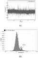
参照图6所示,如图6(a)所示横坐标为采样时间,纵坐标为光电探测器输出的强度值,图6(b)即为大量数据点统计而成的结果图,横坐标为数据点的电压强度值,纵坐标为样本点的个数。聚苯乙烯颗粒漂浮在水中,水的散射信号作为背景必然具有更多的样本数量,颗粒具有比水更高的折射率,因此其信号强度相较背景会更强,而统计数据应满足高斯分布的规律,从图中可以看出左侧的高峰即为统计的背景数据量,右侧小的峰值应为颗粒的散射信号。从信号统计分布上看,颗粒的散射信号强度值与背景散射值可以清晰的分辨出来。Referring to Fig. 6, as shown in Fig. 6(a), the abscissa is the sampling time, the ordinate is the intensity value output by the photodetector, and Fig. 6(b) is the result graph obtained from the statistics of a large number of data points, the abscissa is is the voltage intensity value of the data point, and the ordinate is the number of sample points. Polystyrene particles float in water, and the scattering signal of water must have a larger number of samples as the background. The particles have a higher refractive index than water, so the signal intensity will be stronger than the background, and the statistical data should meet the Gaussian distribution. It can be seen from the figure that the peak on the left is the statistical background data volume, and the small peak on the right should be the scattering signal of the particle. From the statistical distribution of the signal, the scattering signal intensity value of the particles can be clearly distinguished from the background scattering value.
实施例一:Example 1:
参照图7所示,其主要构思是通过翻模方式将结构复制到PDMS上,PDMS 翻模以后便可以形成流道、波导等不同的功能结构。相比于现有技术,本发明既可以实现功能结构的快速、精确成型,又不需要昂贵的设备和复杂的操作流程,从而可以降低微流控芯片的生产成本,有助于微流控芯片的推广。Referring to FIG. 7 , the main idea is to copy the structure to the PDMS by overturning the mold. After the PDMS is overturned, different functional structures such as flow channels and waveguides can be formed. Compared with the prior art, the present invention can realize the rapid and precise forming of the functional structure without requiring expensive equipment and complicated operation procedures, thereby reducing the production cost of the microfluidic chip and helping the microfluidic chip. promotion.
步骤1:制作光刻掩膜版,具体是利用不透明的遮光薄膜在透明基板上形成掩膜图形结构,再通过曝光过程将图形信息转移到衬底基片上。此外,光刻掩膜版中透明基板的材料一般为透明玻璃,遮光膜的材料一般为铬膜。上述制作详细步骤在本发明中不作详述。Step 1: making a photolithography mask, specifically, using an opaque light-shielding film to form a mask pattern structure on a transparent substrate, and then transferring the pattern information to the substrate through an exposure process. In addition, the material of the transparent substrate in the photolithography mask is generally transparent glass, and the material of the light-shielding film is generally a chrome film. The detailed manufacturing steps above are not described in detail in the present invention.
步骤2:匀胶,选择硅片作为基底,将EPG535光刻胶以一定的膜厚度均匀平整地分布在基底表面上。Step 2: Uniform glue, select a silicon wafer as the substrate, and evenly distribute the EPG535 photoresist on the surface of the substrate with a certain film thickness.
步骤3:前烘,匀胶结束后,对匀有EPG535的硅片放到95℃中保持5 分钟,后冷却,将前烘完成的匀有EPG535的硅片冷却至室温,方便后续操作。Step 3: Pre-bake, after the homogenization, put the silicon wafer with EPG535 uniformly at 95°C for 5 minutes, and then cool it down. Cool the pre-baked silicon wafer with EPG535 uniformly to room temperature to facilitate subsequent operations.
步骤4:光刻,将光刻掩膜版覆盖在匀有EPG535的硅片上,并用紫外线进行照射。Step 4: photolithography, cover the photolithography mask on the silicon wafer evenly coated with EPG535, and irradiate it with ultraviolet rays.
步骤5:配置显影液,取5gNaOH固体颗粒溶于1000ml的纯水中,配置5‰的NaOH溶液为光刻胶显影液。Step 5: configure a developer, dissolve 5g of NaOH solid particles in 1000ml of pure water, and configure a 5‰ NaOH solution as a photoresist developer.
步骤6:后烘,匀胶结束后,对匀有EPG535的硅片放到95℃中保持5分钟。后冷却,将后烘完成的光刻完的硅片冷却至室温,方便后续操作。Step 6: Post-bake, after the glue mixing is completed, place the silicon wafer with EPG535 evenly at 95°C for 5 minutes. After post-cooling, the photoetched silicon wafer after post-baking is cooled to room temperature to facilitate subsequent operations.
步骤7:显影,在将冷却好的光刻完的硅片整体侵泡在5‰的NaOH溶液中30s进行显影。步骤4 和8 中,应使用数显电热板,而不是鼓风干燥箱,以免因光刻胶表面优先固化而延缓甚至阻止内层光刻胶溶剂的挥发。将显影过的硅片进行小鼓细流冲洗,直至显影液冲洗干净,并烘干硅片表面残留的水珠。Step 7: development, the whole cooled silicon wafer after photoetching is soaked in NaOH solution of 5‰ for 30s for development. In
步骤8:溅射铝,在整个显影过的硅片表面磁溅射厚度为200纳米的铝膜。Step 8: Sputtering aluminum, and magnetically sputtering an aluminum film with a thickness of 200 nm on the entire surface of the developed silicon wafer.
步骤9:剥离,将溅射铝薄膜的硅片侵泡在丙酮溶液中进行剥离,将侵泡过丙酮溶液的硅片用酒精进行冲洗去除表面的丙酮残夜,而后继续用纯水流冲洗,直至表面冲洗干净,并烘干表面残留的水珠。Step 9: peel off, soak the silicon wafer with the sputtered aluminum film in the acetone solution for peeling, rinse the silicon wafer soaked in the acetone solution with alcohol to remove the acetone residue on the surface, and then continue to rinse with pure water, Rinse until the surface is clean and dry any remaining water droplets on the surface.
步骤10:刻蚀,将剥离完成的硅片进行干法刻蚀,根据需求设定刻蚀深度。上述制作详细步骤在本发明中不作详述。Step 10: Etching, performing dry etching on the stripped silicon wafer, and setting the etching depth according to requirements. The detailed manufacturing steps above are not described in detail in the present invention.
步骤11:配置PDMS翻模溶液,PDMS常温下以液态存在,加入固化剂以后加热固化。配置的时候,PDMS和固化剂按照质量分数10:1配比,由于PDMS粘度比较大,为了使固化剂充分混合到PDMS溶液中去,必须用搅拌棒充分搅拌。不可避免的在搅拌过程中,会产生大量的气泡。气泡的存在会破坏流道结构,而且会影响观察。所以需要将配置好的混合剂放在真空干燥箱中抽取真空以便将气泡抽取出来。步骤中的真空干燥箱,应在常温状态下使用防止PDMS翻模溶液提前固化。Step 11: Prepare the PDMS mold turning solution. PDMS exists in a liquid state at room temperature. After adding a curing agent, it is heated and cured. When configuring, PDMS and curing agent are in a ratio of 10:1 by mass fraction. Due to the relatively high viscosity of PDMS, in order to fully mix the curing agent into the PDMS solution, it must be fully stirred with a stirring rod. Inevitably, a lot of air bubbles will be generated during the stirring process. The presence of air bubbles will damage the flow channel structure and will affect the observation. Therefore, it is necessary to place the prepared mixture in a vacuum drying oven to draw a vacuum to extract the air bubbles. The vacuum drying oven in the step should be used to prevent the PDMS from turning over the mold solution at room temperature to cure in advance.
步骤13:浇注,经过抽真空处理的PDMS翻模溶液透明清澈,接下来将PDMS翻模溶液浇注到放有刻蚀好的硅片的培养皿中,在浇注过程中注意溶液应该不存在气泡,如果存在气泡可以通过不锈钢针的针尖将气泡戳破,以防止气泡影响结构精度。选择浇注厚度约为3-5mm,为了避免结构太薄的不稳定性,以及太厚造成的成像不清晰。将培养皿静置到溶液表面平整,最后将其放到烘烤台,温度75℃保温半小时使得PDMS固化,然后冷却到室温。Step 13: Pouring, the PDMS turning solution after vacuum treatment is transparent and clear, then pour the PDMS turning solution into a petri dish with etched silicon wafers. During the pouring process, pay attention to the solution There should be no bubbles, If there are air bubbles, the air bubbles can be punctured by the tip of the stainless steel needle to prevent the air bubbles from affecting the accuracy of the structure. The casting thickness is selected to be about 3-5mm, in order to avoid the instability of the structure that is too thin, and the unclear imaging caused by too thick. The petri dish was allowed to stand until the surface of the solution was flat, and finally placed on a baking table, kept at 75°C for half an hour to solidify the PDMS, and then cooled to room temperature.
步骤14:翻模,固化好的PDMS在整个培养皿中,先用尖头的切割刀从结构边缘部位切割PDMS,待PDMS与培养皿整个边缘脱离以后轻轻的从不同部位掀起PDMS,将揭下来的PDMS放在新鲜的保鲜膜上,上方也覆盖保鲜膜,防止灰尘污染表面。Step 14: Turn the mold over, the cured PDMS is placed in the entire petri dish, first cut the PDMS from the edge of the structure with a sharp cutting knife, after the PDMS is separated from the entire edge of the petri dish, gently lift the PDMS from different parts to remove the The downed PDMS is placed on fresh plastic wrap, and the top is also covered with plastic wrap to prevent dust from contaminating the surface.
步骤15:键合,将PDMS置于等离子清洗机中进行电子轰击,进行等离子体表面活性处理,处理完成的PDMS粘附到提前制备的PDMS基底上,静置直至键合牢固。Step 15: Bonding, placing the PDMS in a plasma cleaning machine for electron bombardment, and performing plasma surface active treatment. The treated PDMS is adhered to the PDMS substrate prepared in advance, and is allowed to stand until the bonding is firm.
步骤5、步骤11不分先后,可以按照实际要求调整进行的顺序。
以上步骤除了可以进行芯片的制作之外,还可以进行键合PDMS基底的制作,其中PDMS制取与上述方式相同,即先制备PDMS翻模溶液,然后将PDMS翻模溶液浇注到放置平板基底的培养皿中,待溶液表面平整,将其放到烘烤台加热固化,根据所需大小割取相应的PDMS基底,并延边缘掀起PDMS基底,将揭下来的PDMS基底平放在新鲜的保鲜膜上,上方也覆盖保鲜膜,防止灰尘污染表面。制取PDMS基底的放置培养皿中的平板基底可以是硅片,玻璃等较稳定的固体平板。In addition to the fabrication of chips, the above steps can also be used to fabricate bonded PDMS substrates. The preparation of PDMS is the same as the above-mentioned method, that is, the PDMS overturning solution is prepared first, and then the PDMS overturning solution is poured into the place where the flat substrate is placed. In the petri dish, when the surface of the solution is flat, put it on the baking table to heat and solidify, cut the corresponding PDMS substrate according to the required size, lift the PDMS substrate along the edge, and lay the removed PDMS substrate flat on a fresh plastic wrap. The top and top are also covered with plastic wrap to prevent dust from contaminating the surface. The plate substrate placed in the petri dish for preparing the PDMS substrate can be a relatively stable solid plate such as silicon wafer and glass.
以上步骤除了可以进行芯片的制取,还可以实验微流道深度的调整,其具体的调整方式是:通过调整刻蚀深度,可以调整翻模时候流道的形成高度从而调整芯片流道深度。The above steps can not only prepare the chip, but also experiment with adjusting the depth of the microchannel.
以上是对基于准贝塞尔光波导结构的免标记活细胞检测微流控芯片的制造工艺的具体说明,但本发明制造工艺并不限于所述步骤,熟悉本领域的技术人员在不违背本发明精神前提下还可做出种种等同变形或替换,这些等同的变形或替换均包含在本发明要求所限定的范围内。The above is a specific description of the manufacturing process of the label-free live cell detection microfluidic chip based on the quasi-Béssel optical waveguide structure, but the manufacturing process of the present invention is not limited to the above steps, and those skilled in the art will not violate the present invention. Various equivalent modifications or substitutions can also be made under the premise of the spirit of the invention, and these equivalent modifications or substitutions are all included within the scope defined by the requirements of the present invention.
基于准贝塞尔光波导结构的免标记活细胞检测微流控芯片制作完成后,按照图5搭建控检测平台,确保流道通畅及光束调制合乎设计要求;After the label-free living cell detection microfluidic chip based on the quasi-Bessel optical waveguide structure is fabricated, a control and detection platform is built according to Figure 5 to ensure that the flow channel is unobstructed and the beam modulation meets the design requirements;
(1)按照图5,将光纤激光器的光纤接入芯片的入射光纤耦合波导结构,光电探测器的光纤接入芯片的光纤定位结构;将电控注液泵的样本注入口,缓冲液注入口连接芯片样本液入口端和缓冲液入口端;(1) According to Figure 5, connect the fiber of the fiber laser to the incident fiber coupling waveguide structure of the chip, and the fiber of the photodetector to the fiber positioning structure of the chip; connect the sample injection port of the electronically controlled liquid injection pump and the buffer injection port Connect the chip sample liquid inlet port and the buffer inlet port;
(2)配制样本液,采用16.5μm的聚苯乙烯小球作为探测样本与纯水配置样本液。通过电控注液泵的样本注入口,缓冲液注入口注入样本液以及缓冲液;(2) Prepare a sample solution, using 16.5 μm polystyrene beads as the detection sample and pure water to prepare the sample solution. The sample solution and buffer solution are injected through the sample injection port and buffer injection port of the electronically controlled injection pump;
(3)开启电控注液泵,调整样本液和缓冲液的流速配比,经过样本液入口和缓冲液入口注入芯片,液体经过流体聚焦微通道结构在流体聚焦区域形成稳定的流体聚焦,并在探测区域形成较细的稳定在流道中心的样本流,废液经由废液流出口流出;(3) Turn on the electronically controlled injection pump, adjust the flow rate ratio of the sample solution and the buffer solution, and inject into the chip through the sample solution inlet and the buffer solution inlet. The liquid forms a stable fluid focus in the fluid focus area through the fluid focusing microchannel structure, and In the detection area, a thin and stable sample flow is formed in the center of the flow channel, and the waste liquid flows out through the waste liquid outlet;
(4)打开激光器,将高斯光束通过准贝塞尔光束调控波导结构产生准贝塞尔探测光束,对流道中心流经的样本进行辐照;(4) Turn on the laser, pass the Gaussian beam through the quasi-Béssel beam control waveguide structure to generate a quasi-Béssel probe beam, and irradiate the sample flowing through the center of the flow channel;
(5)开启光电探测器,调节合适的量程及采样频率,接收准贝塞尔光束辐照细胞后产生的散射信号;(5) Turn on the photodetector, adjust the appropriate range and sampling frequency, and receive the scattered signal generated after the quasi-Béssel beam irradiates the cell;
(6)光电探测器将采集到的信号存储信号采集卡中,如图6(a);通过存储计算机matlab对数据进行统计,制作成图表6(b)进行分析;(6) The photodetector stores the collected signal in the signal acquisition card, as shown in Figure 6 (a); the data is counted by the storage computer matlab, and is made into Figure 6 (b) for analysis;
实验结论:Experimental results:
本发明在微流控芯片前端设计并实现具有自我修复束型能力的不易发生衍射的准贝塞尔光束波导结构,从而解决入射光束发散角控制问题,提高微流控芯片内细胞散射前向小角度重要光信息的信噪比;在微流控芯片接收端设计免标记细胞散射接收波导结构,能够将某一角度散射信号精准导出并聚焦,实现高精度的微流控系统内的免标记细胞识别与分类。本设计中的微流控芯片无需改变生物颗粒的原始生理状态,无需对生物样本进行任何化学染色等处理,避免了实验操作中不一致性等问题导致的样品识别错误等问题;样本颗粒检测方法简单,无需依赖操作人员的从业经验,同时无需使用任何具有毒性、环境破坏性等化学物质;基于准贝塞尔光波导结构的免标记活细胞检测微流控芯片,有望为临床医学检测提供一种绿色化的活体细胞检测新方法。The invention designs and realizes a quasi-Béssel beam waveguide structure with self-repairing beam shape capability at the front end of the microfluidic chip, which is not easy to generate diffraction, thereby solving the problem of controlling the divergence angle of the incident beam, and improving the small forward scattering of cells in the microfluidic chip. The signal-to-noise ratio of the angle-important optical information; the label-free cell scattering and receiving waveguide structure is designed at the receiving end of the microfluidic chip, which can accurately export and focus the scattered signal at a certain angle, and realize the label-free cells in the high-precision microfluidic system. Identify and classify. The microfluidic chip in this design does not need to change the original physiological state of biological particles, and does not need to perform any chemical staining and other processing on biological samples, which avoids problems such as sample identification errors caused by inconsistency in experimental operations; the sample particle detection method is simple , without relying on the operator's experience, and without using any toxic, environmentally destructive and other chemical substances; the label-free living cell detection microfluidic chip based on the quasi-Bessel optical waveguide structure is expected to provide a clinical medical detection. A new method for the detection of green living cells.
Claims (3)
Priority Applications (1)
| Application Number | Priority Date | Filing Date | Title |
|---|---|---|---|
| CN201910468904.XACN110237875B (en) | 2019-05-31 | 2019-05-31 | Mark-free living cell detection micro-fluidic chip based on quasi-Bessel optical waveguide structure |
Applications Claiming Priority (1)
| Application Number | Priority Date | Filing Date | Title |
|---|---|---|---|
| CN201910468904.XACN110237875B (en) | 2019-05-31 | 2019-05-31 | Mark-free living cell detection micro-fluidic chip based on quasi-Bessel optical waveguide structure |
Publications (2)
| Publication Number | Publication Date |
|---|---|
| CN110237875A CN110237875A (en) | 2019-09-17 |
| CN110237875Btrue CN110237875B (en) | 2020-11-10 |
Family
ID=67885668
Family Applications (1)
| Application Number | Title | Priority Date | Filing Date |
|---|---|---|---|
| CN201910468904.XAExpired - Fee RelatedCN110237875B (en) | 2019-05-31 | 2019-05-31 | Mark-free living cell detection micro-fluidic chip based on quasi-Bessel optical waveguide structure |
Country Status (1)
| Country | Link |
|---|---|
| CN (1) | CN110237875B (en) |
Families Citing this family (5)
| Publication number | Priority date | Publication date | Assignee | Title |
|---|---|---|---|---|
| CN110724627B (en)* | 2019-11-15 | 2022-12-09 | 长春长光辰英生物科学仪器有限公司 | Sample bacterial colony positioning device and positioning method of single cell sorter |
| CN111751263A (en)* | 2020-06-08 | 2020-10-09 | 西安交通大学 | Inversion method of two-dimensional scattering images of label-free cells based on gray level co-occurrence matrix |
| CN111921469B (en)* | 2020-08-24 | 2024-08-13 | 天津大学 | Notebook type step type emulsifying or reacting micro device module |
| CN112625900B (en)* | 2020-12-17 | 2022-05-17 | 西安电子科技大学 | Experimental device for electromagnetic irradiation of cells with tilted waveguide resonator |
| CN114317234B (en)* | 2022-01-14 | 2023-06-27 | 西安交通大学 | Multi-pathogen rapid detection type micro-fluidic system based on module structure |
Family Cites Families (10)
| Publication number | Priority date | Publication date | Assignee | Title |
|---|---|---|---|---|
| JP5461205B2 (en)* | 2010-01-19 | 2014-04-02 | 日立造船株式会社 | Laser processing method and apparatus |
| GB201220478D0 (en)* | 2012-11-14 | 2012-12-26 | Univ Dundee | Tunable laser for fluorescence microscopy |
| US20180321233A1 (en)* | 2017-05-02 | 2018-11-08 | Sanguis LLC | System, Device and Method for Counting Desired Cells in a Body Fluid |
| CN109570781A (en)* | 2017-09-28 | 2019-04-05 | 上海微电子装备(集团)股份有限公司 | A kind of microwell array processing unit (plant) and method |
| CN107773217B (en)* | 2017-09-29 | 2021-01-05 | 天津大学 | Living tissue microcirculation metabolism dynamic measuring device and method |
| CN107907983A (en)* | 2017-10-31 | 2018-04-13 | 昆明理工大学 | Digital holographic microscopy device and its method of work based on bottle beams illumination |
| CN108444897B (en)* | 2018-03-06 | 2021-04-13 | 山东大学 | Label-free microfluidic cytometer based on light sheet illumination and sheath flow technology and method |
| CN108855255A (en)* | 2018-04-17 | 2018-11-23 | 华中科技大学 | Measure micro-fluidic chip, preparation method and the application of dynamic light scattering |
| CN108873171B (en)* | 2018-07-16 | 2020-06-16 | 哈尔滨工程大学 | A multi-core fiber-like Bessel beam array optical tweezers |
| CN109683330B (en)* | 2019-01-30 | 2021-04-30 | 复旦大学 | Method for generating Bessel-like light beam by growing micro-cone on end face of optical fiber |
- 2019
- 2019-05-31CNCN201910468904.XApatent/CN110237875B/ennot_activeExpired - Fee Related
Also Published As
| Publication number | Publication date |
|---|---|
| CN110237875A (en) | 2019-09-17 |
Similar Documents
| Publication | Publication Date | Title |
|---|---|---|
| CN110237875B (en) | Mark-free living cell detection micro-fluidic chip based on quasi-Bessel optical waveguide structure | |
| US12174403B2 (en) | Manufacturing method for diffraction grating waveguide of near-eye display | |
| CN101118380B (en) | Imprint method and imprint device | |
| CN102998242B (en) | Micro-fluid cytometer and manufacture method thereof | |
| Queval et al. | Chamber and microfluidic probe for microperfusion of organotypic brain slices | |
| CN104941706B (en) | A kind of twin channel chip of light stream miniflow and preparation method thereof | |
| WO2018040277A1 (en) | Method for manufacturing multilayer microfluidic chip suitable for batch production | |
| CN110007451A (en) | A kind of metasurface microscope, preparation method thereof, and optical path measurement system | |
| JP5182097B2 (en) | Manufacturing method of optical waveguide module | |
| CN110554448A (en) | Artificial compound eye with adjustable large eye curvature, preparation method and application | |
| CN111474106A (en) | Methods and systems for determining mechanical properties of biological cells or biological cell-like particles | |
| Cheong et al. | Using a microfluidic device for high-content analysis of cell signaling | |
| JPWO2018105608A1 (en) | Particle trapping device | |
| Hafttananian et al. | Integratable micro-optical compound objective lens using soft lithography | |
| Zhong et al. | Fabrication of a microfluidic system with in situ-integrated microlens arrays using electrohydrodynamic jet printing | |
| Sum et al. | Proton beam writing of passive polymer optical waveguides | |
| Rochman et al. | Single cell volume measurement utilizing the Fluorescence Exclusion Method (FXm) | |
| CN117890334A (en) | A single cell fluorescence scattered light detection and image reconstruction integrated method and device | |
| Sugioka et al. | 3D micromachining of photosensitive glass by femtosecond laser for microreactor manufacture | |
| JPWO2007077899A1 (en) | Resin plate, method for producing the same, and cell culture container provided with resin plate | |
| CN102455464B (en) | Optical waveguide production method | |
| CN218272775U (en) | A glass-based planar waveguide for dark-field fluorescence microscopy | |
| CN113866972B (en) | Blood cell analyzer adopting micro optical technology | |
| Suryana et al. | Soft Lithographic Procedure for Producing Plastic Microfluidic Devices with View-ports Transparent to Visible and Infrared Light | |
| Yang et al. | Design and fabrication of an on-chip micro flow cytometer with integrated micro-lens |
Legal Events
| Date | Code | Title | Description |
|---|---|---|---|
| PB01 | Publication | ||
| PB01 | Publication | ||
| SE01 | Entry into force of request for substantive examination | ||
| SE01 | Entry into force of request for substantive examination | ||
| GR01 | Patent grant | ||
| GR01 | Patent grant | ||
| CF01 | Termination of patent right due to non-payment of annual fee | ||
| CF01 | Termination of patent right due to non-payment of annual fee | Granted publication date:20201110 |