CN110189639B - Display substrate, display panel and display device - Google Patents
Display substrate, display panel and display deviceDownload PDFInfo
- Publication number
- CN110189639B CN110189639BCN201910580310.8ACN201910580310ACN110189639BCN 110189639 BCN110189639 BCN 110189639BCN 201910580310 ACN201910580310 ACN 201910580310ACN 110189639 BCN110189639 BCN 110189639B
- Authority
- CN
- China
- Prior art keywords
- electrode
- display area
- sub
- display
- pixel
- Prior art date
- Legal status (The legal status is an assumption and is not a legal conclusion. Google has not performed a legal analysis and makes no representation as to the accuracy of the status listed.)
- Active
Links
- 239000000758substrateSubstances0.000titleclaimsabstractdescription141
- 238000002834transmittanceMethods0.000claimsabstractdescription34
- 238000000034methodMethods0.000claimsdescription24
- 239000003990capacitorSubstances0.000claimsdescription20
- 239000000463materialSubstances0.000claimsdescription19
- AMGQUBHHOARCQH-UHFFFAOYSA-Nindium;oxotinChemical compound[In].[Sn]=OAMGQUBHHOARCQH-UHFFFAOYSA-N0.000claimsdescription17
- BQCADISMDOOEFD-UHFFFAOYSA-NSilverChemical compound[Ag]BQCADISMDOOEFD-UHFFFAOYSA-N0.000claimsdescription16
- 229910052709silverInorganic materials0.000claimsdescription16
- 239000004332silverSubstances0.000claimsdescription16
- YVTHLONGBIQYBO-UHFFFAOYSA-Nzinc indium(3+) oxygen(2-)Chemical compound[O--].[Zn++].[In+3]YVTHLONGBIQYBO-UHFFFAOYSA-N0.000claimsdescription16
- 241000219122CucurbitaSpecies0.000claimsdescription8
- 235000009852Cucurbita pepoNutrition0.000claimsdescription8
- PXHVJJICTQNCMI-UHFFFAOYSA-NNickelChemical compound[Ni]PXHVJJICTQNCMI-UHFFFAOYSA-N0.000claimsdescription6
- RTAQQCXQSZGOHL-UHFFFAOYSA-NTitaniumChemical compound[Ti]RTAQQCXQSZGOHL-UHFFFAOYSA-N0.000claimsdescription5
- 238000005538encapsulationMethods0.000claimsdescription5
- 239000010936titaniumSubstances0.000claimsdescription5
- 229910052719titaniumInorganic materials0.000claimsdescription5
- FYYHWMGAXLPEAU-UHFFFAOYSA-NMagnesiumChemical compound[Mg]FYYHWMGAXLPEAU-UHFFFAOYSA-N0.000claimsdescription4
- 229910052782aluminiumInorganic materials0.000claimsdescription4
- XAGFODPZIPBFFR-UHFFFAOYSA-NaluminiumChemical compound[Al]XAGFODPZIPBFFR-UHFFFAOYSA-N0.000claimsdescription4
- 229910052749magnesiumInorganic materials0.000claimsdescription4
- 239000011777magnesiumSubstances0.000claimsdescription4
- SJCKRGFTWFGHGZ-UHFFFAOYSA-Nmagnesium silverChemical compound[Mg].[Ag]SJCKRGFTWFGHGZ-UHFFFAOYSA-N0.000claimsdescription4
- VYZAMTAEIAYCRO-UHFFFAOYSA-NChromiumChemical compound[Cr]VYZAMTAEIAYCRO-UHFFFAOYSA-N0.000claimsdescription3
- RYGMFSIKBFXOCR-UHFFFAOYSA-NCopperChemical compound[Cu]RYGMFSIKBFXOCR-UHFFFAOYSA-N0.000claimsdescription3
- ZOKXTWBITQBERF-UHFFFAOYSA-NMolybdenumChemical compound[Mo]ZOKXTWBITQBERF-UHFFFAOYSA-N0.000claimsdescription3
- HCHKCACWOHOZIP-UHFFFAOYSA-NZincChemical compound[Zn]HCHKCACWOHOZIP-UHFFFAOYSA-N0.000claimsdescription3
- 229910052804chromiumInorganic materials0.000claimsdescription3
- 239000011651chromiumSubstances0.000claimsdescription3
- 229910052802copperInorganic materials0.000claimsdescription3
- 239000010949copperSubstances0.000claimsdescription3
- PCHJSUWPFVWCPO-UHFFFAOYSA-NgoldChemical compound[Au]PCHJSUWPFVWCPO-UHFFFAOYSA-N0.000claimsdescription3
- 229910052737goldInorganic materials0.000claimsdescription3
- 239000010931goldSubstances0.000claimsdescription3
- 229910052750molybdenumInorganic materials0.000claimsdescription3
- 239000011733molybdenumSubstances0.000claimsdescription3
- 229910052759nickelInorganic materials0.000claimsdescription3
- WFKWXMTUELFFGS-UHFFFAOYSA-NtungstenChemical compound[W]WFKWXMTUELFFGS-UHFFFAOYSA-N0.000claimsdescription3
- 229910052721tungstenInorganic materials0.000claimsdescription3
- 239000010937tungstenSubstances0.000claimsdescription3
- 229910052725zincInorganic materials0.000claimsdescription3
- 239000011701zincSubstances0.000claimsdescription3
- 238000004806packaging method and processMethods0.000claimsdescription2
- 239000010410layerSubstances0.000description149
- 230000000694effectsEffects0.000description22
- 238000010586diagramMethods0.000description10
- 239000011229interlayerSubstances0.000description8
- 230000009286beneficial effectEffects0.000description6
- 230000007547defectEffects0.000description6
- 239000004065semiconductorSubstances0.000description6
- 229910052751metalInorganic materials0.000description5
- 239000002184metalSubstances0.000description5
- 230000015556catabolic processEffects0.000description4
- 238000006731degradation reactionMethods0.000description4
- 238000003384imaging methodMethods0.000description4
- 238000001704evaporationMethods0.000description3
- 238000009826distributionMethods0.000description2
- 230000008020evaporationEffects0.000description2
- 238000004519manufacturing processMethods0.000description2
- 230000000737periodic effectEffects0.000description2
- 238000002360preparation methodMethods0.000description2
- 230000003313weakening effectEffects0.000description2
- 230000006978adaptationEffects0.000description1
- 230000000295complement effectEffects0.000description1
- 239000004020conductorSubstances0.000description1
- 238000007796conventional methodMethods0.000description1
- 238000012986modificationMethods0.000description1
- 230000004048modificationEffects0.000description1
- 230000002441reversible effectEffects0.000description1
- 238000003860storageMethods0.000description1
- 230000037303wrinklesEffects0.000description1
Images


Classifications
- G—PHYSICS
- G09—EDUCATION; CRYPTOGRAPHY; DISPLAY; ADVERTISING; SEALS
- G09F—DISPLAYING; ADVERTISING; SIGNS; LABELS OR NAME-PLATES; SEALS
- G09F9/00—Indicating arrangements for variable information in which the information is built-up on a support by selection or combination of individual elements
- G09F9/30—Indicating arrangements for variable information in which the information is built-up on a support by selection or combination of individual elements in which the desired character or characters are formed by combining individual elements
- H—ELECTRICITY
- H10—SEMICONDUCTOR DEVICES; ELECTRIC SOLID-STATE DEVICES NOT OTHERWISE PROVIDED FOR
- H10K—ORGANIC ELECTRIC SOLID-STATE DEVICES
- H10K59/00—Integrated devices, or assemblies of multiple devices, comprising at least one organic light-emitting element covered by group H10K50/00
- H10K59/30—Devices specially adapted for multicolour light emission
- H10K59/35—Devices specially adapted for multicolour light emission comprising red-green-blue [RGB] subpixels
- H10K59/353—Devices specially adapted for multicolour light emission comprising red-green-blue [RGB] subpixels characterised by the geometrical arrangement of the RGB subpixels
- G—PHYSICS
- G09—EDUCATION; CRYPTOGRAPHY; DISPLAY; ADVERTISING; SEALS
- G09G—ARRANGEMENTS OR CIRCUITS FOR CONTROL OF INDICATING DEVICES USING STATIC MEANS TO PRESENT VARIABLE INFORMATION
- G09G3/00—Control arrangements or circuits, of interest only in connection with visual indicators other than cathode-ray tubes
- G09G3/20—Control arrangements or circuits, of interest only in connection with visual indicators other than cathode-ray tubes for presentation of an assembly of a number of characters, e.g. a page, by composing the assembly by combination of individual elements arranged in a matrix no fixed position being assigned to or needed to be assigned to the individual characters or partial characters
- G09G3/22—Control arrangements or circuits, of interest only in connection with visual indicators other than cathode-ray tubes for presentation of an assembly of a number of characters, e.g. a page, by composing the assembly by combination of individual elements arranged in a matrix no fixed position being assigned to or needed to be assigned to the individual characters or partial characters using controlled light sources
- G09G3/30—Control arrangements or circuits, of interest only in connection with visual indicators other than cathode-ray tubes for presentation of an assembly of a number of characters, e.g. a page, by composing the assembly by combination of individual elements arranged in a matrix no fixed position being assigned to or needed to be assigned to the individual characters or partial characters using controlled light sources using electroluminescent panels
- G09G3/32—Control arrangements or circuits, of interest only in connection with visual indicators other than cathode-ray tubes for presentation of an assembly of a number of characters, e.g. a page, by composing the assembly by combination of individual elements arranged in a matrix no fixed position being assigned to or needed to be assigned to the individual characters or partial characters using controlled light sources using electroluminescent panels semiconductive, e.g. using light-emitting diodes [LED]
- H—ELECTRICITY
- H04—ELECTRIC COMMUNICATION TECHNIQUE
- H04N—PICTORIAL COMMUNICATION, e.g. TELEVISION
- H04N23/00—Cameras or camera modules comprising electronic image sensors; Control thereof
- H04N23/57—Mechanical or electrical details of cameras or camera modules specially adapted for being embedded in other devices
- H—ELECTRICITY
- H10—SEMICONDUCTOR DEVICES; ELECTRIC SOLID-STATE DEVICES NOT OTHERWISE PROVIDED FOR
- H10H—INORGANIC LIGHT-EMITTING SEMICONDUCTOR DEVICES HAVING POTENTIAL BARRIERS
- H10H20/00—Individual inorganic light-emitting semiconductor devices having potential barriers, e.g. light-emitting diodes [LED]
- H10H20/80—Constructional details
- H10H20/83—Electrodes
- H10H20/831—Electrodes characterised by their shape
- H10H20/8312—Electrodes characterised by their shape extending at least partially through the bodies
- H—ELECTRICITY
- H10—SEMICONDUCTOR DEVICES; ELECTRIC SOLID-STATE DEVICES NOT OTHERWISE PROVIDED FOR
- H10H—INORGANIC LIGHT-EMITTING SEMICONDUCTOR DEVICES HAVING POTENTIAL BARRIERS
- H10H20/00—Individual inorganic light-emitting semiconductor devices having potential barriers, e.g. light-emitting diodes [LED]
- H10H20/80—Constructional details
- H10H20/83—Electrodes
- H10H20/832—Electrodes characterised by their material
- H10H20/833—Transparent materials
- H—ELECTRICITY
- H10—SEMICONDUCTOR DEVICES; ELECTRIC SOLID-STATE DEVICES NOT OTHERWISE PROVIDED FOR
- H10H—INORGANIC LIGHT-EMITTING SEMICONDUCTOR DEVICES HAVING POTENTIAL BARRIERS
- H10H20/00—Individual inorganic light-emitting semiconductor devices having potential barriers, e.g. light-emitting diodes [LED]
- H10H20/80—Constructional details
- H10H20/85—Packages
- H10H20/855—Optical field-shaping means, e.g. lenses
- H—ELECTRICITY
- H10—SEMICONDUCTOR DEVICES; ELECTRIC SOLID-STATE DEVICES NOT OTHERWISE PROVIDED FOR
- H10H—INORGANIC LIGHT-EMITTING SEMICONDUCTOR DEVICES HAVING POTENTIAL BARRIERS
- H10H20/00—Individual inorganic light-emitting semiconductor devices having potential barriers, e.g. light-emitting diodes [LED]
- H10H20/80—Constructional details
- H10H20/85—Packages
- H10H20/857—Interconnections, e.g. lead-frames, bond wires or solder balls
- H—ELECTRICITY
- H10—SEMICONDUCTOR DEVICES; ELECTRIC SOLID-STATE DEVICES NOT OTHERWISE PROVIDED FOR
- H10H—INORGANIC LIGHT-EMITTING SEMICONDUCTOR DEVICES HAVING POTENTIAL BARRIERS
- H10H29/00—Integrated devices, or assemblies of multiple devices, comprising at least one light-emitting semiconductor element covered by group H10H20/00
- H10H29/10—Integrated devices comprising at least one light-emitting semiconductor component covered by group H10H20/00
- H10H29/14—Integrated devices comprising at least one light-emitting semiconductor component covered by group H10H20/00 comprising multiple light-emitting semiconductor components
- H10H29/142—Two-dimensional arrangements, e.g. asymmetric LED layout
- H—ELECTRICITY
- H10—SEMICONDUCTOR DEVICES; ELECTRIC SOLID-STATE DEVICES NOT OTHERWISE PROVIDED FOR
- H10K—ORGANIC ELECTRIC SOLID-STATE DEVICES
- H10K59/00—Integrated devices, or assemblies of multiple devices, comprising at least one organic light-emitting element covered by group H10K50/00
- H10K59/10—OLED displays
- H10K59/12—Active-matrix OLED [AMOLED] displays
- H10K59/122—Pixel-defining structures or layers, e.g. banks
- H—ELECTRICITY
- H10—SEMICONDUCTOR DEVICES; ELECTRIC SOLID-STATE DEVICES NOT OTHERWISE PROVIDED FOR
- H10K—ORGANIC ELECTRIC SOLID-STATE DEVICES
- H10K59/00—Integrated devices, or assemblies of multiple devices, comprising at least one organic light-emitting element covered by group H10K50/00
- H10K59/10—OLED displays
- H10K59/12—Active-matrix OLED [AMOLED] displays
- H10K59/123—Connection of the pixel electrodes to the thin film transistors [TFT]
- H—ELECTRICITY
- H10—SEMICONDUCTOR DEVICES; ELECTRIC SOLID-STATE DEVICES NOT OTHERWISE PROVIDED FOR
- H10K—ORGANIC ELECTRIC SOLID-STATE DEVICES
- H10K59/00—Integrated devices, or assemblies of multiple devices, comprising at least one organic light-emitting element covered by group H10K50/00
- H10K59/10—OLED displays
- H10K59/12—Active-matrix OLED [AMOLED] displays
- H10K59/131—Interconnections, e.g. wiring lines or terminals
- H10K59/1315—Interconnections, e.g. wiring lines or terminals comprising structures specially adapted for lowering the resistance
- H—ELECTRICITY
- H10—SEMICONDUCTOR DEVICES; ELECTRIC SOLID-STATE DEVICES NOT OTHERWISE PROVIDED FOR
- H10K—ORGANIC ELECTRIC SOLID-STATE DEVICES
- H10K59/00—Integrated devices, or assemblies of multiple devices, comprising at least one organic light-emitting element covered by group H10K50/00
- H10K59/80—Constructional details
- H10K59/8794—Arrangements for heating and cooling
- H—ELECTRICITY
- H10—SEMICONDUCTOR DEVICES; ELECTRIC SOLID-STATE DEVICES NOT OTHERWISE PROVIDED FOR
- H10K—ORGANIC ELECTRIC SOLID-STATE DEVICES
- H10K59/00—Integrated devices, or assemblies of multiple devices, comprising at least one organic light-emitting element covered by group H10K50/00
- H10K59/60—OLEDs integrated with inorganic light-sensitive elements, e.g. with inorganic solar cells or inorganic photodiodes
- H10K59/65—OLEDs integrated with inorganic image sensors
Landscapes
- Engineering & Computer Science (AREA)
- Microelectronics & Electronic Packaging (AREA)
- Physics & Mathematics (AREA)
- General Physics & Mathematics (AREA)
- Theoretical Computer Science (AREA)
- Multimedia (AREA)
- Signal Processing (AREA)
- Computer Hardware Design (AREA)
- Devices For Indicating Variable Information By Combining Individual Elements (AREA)
- Electroluminescent Light Sources (AREA)
Abstract
Translated fromChinese
Description
Translated fromChinese技术领域technical field
本申请涉及显示技术领域,尤其涉及一种显示基板、显示面板及显示装置。The present application relates to the field of display technology, and in particular, to a display substrate, a display panel and a display device.
背景技术Background technique
随着电子设备的快速发展,用户对屏占比的要求越来越高,使得电子设备的全面屏显示受到业界越来越多的关注。传统的电子设备如手机、平板电脑等,由于需要集成诸如前置摄像头、听筒以及红外感应元件等,故而可通过在显示屏上开槽(Notch),在开槽区域设置摄像头、听筒以及红外感应元件等,但开槽区域并不能用来显示画面,如现有技术中的刘海屏,或者采用在屏幕上开孔的方式,对于实现摄像功能的电子设备来说,外界光线可通过屏幕上的开孔处进入位于屏幕下方的感光元件。但是这些电子设备均不是真正意义上的全面屏,并不能在整个屏幕的各个区域均进行显示,如在摄像头区域不能显示画面。With the rapid development of electronic devices, users have higher and higher requirements for screen-to-body ratio, making the full-screen display of electronic devices attract more and more attention in the industry. Traditional electronic devices such as mobile phones, tablet computers, etc. need to integrate such as front cameras, earpieces and infrared sensing elements, etc., so the camera, earpieces and infrared sensors can be set in the notch area by notching on the display screen. components, etc., but the slotted area cannot be used to display the picture, such as Liu Haiping in the prior art, or the method of opening holes on the screen. For electronic equipment that realizes the camera function, the external light can pass through the screen on the screen. The opening enters the photosensitive element located below the screen. However, these electronic devices are not full-screen in the true sense, and cannot be displayed in all areas of the entire screen, for example, images cannot be displayed in the camera area.
发明内容SUMMARY OF THE INVENTION
根据本申请实施例的第一方面,提供了一种显示基板,所述显示基板包括第一显示区和第二显示区;所述第一显示区的透光率大于所述第二显示区的透光率;According to a first aspect of the embodiments of the present application, a display substrate is provided, the display substrate includes a first display area and a second display area; the light transmittance of the first display area is greater than that of the second display area Transmittance;
所述第一显示区内设有多个第一子像素,所述第一子像素包括第一电极、设置在所述第一电极上的发光结构及设置在所述发光结构上的第二电极,用于驱动所述第一子像素的像素电路设置在所述第二显示区内,所述第一子像素的第一电极通过走线与对应的像素电路电连接,所述走线包括互相连接的第一段和第二段,所述第一段位于所述第一显示区,所述第二段位于所述第二显示区;A plurality of first sub-pixels are arranged in the first display area, and the first sub-pixels include a first electrode, a light-emitting structure arranged on the first electrode, and a second electrode arranged on the light-emitting structure , the pixel circuit for driving the first sub-pixel is arranged in the second display area, and the first electrode of the first sub-pixel is electrically connected to the corresponding pixel circuit through wiring, and the wiring includes The first segment and the second segment are connected, the first segment is located in the first display area, and the second segment is located in the second display area;
所述第一显示区内还设置有导电层,所述第一电极通过所述导电层与所述第一段电连接,所述导电层的电阻率分别小于所述第一电极的电阻率及所述第一段的电阻率。A conductive layer is also arranged in the first display area, the first electrode is electrically connected to the first segment through the conductive layer, and the resistivity of the conductive layer is respectively smaller than that of the first electrode and the resistivity of the first segment.
在一个实施例中,所述第一电极位于所述导电层和所述第一段上方,所述第一电极与所述第一段之间设置有第一绝缘层,所述第一绝缘层上设置有通孔,所述第一电极通过所述通孔与所述导电层接触。In one embodiment, the first electrode is located above the conductive layer and the first segment, a first insulating layer is disposed between the first electrode and the first segment, and the first insulating layer A through hole is provided thereon, and the first electrode is in contact with the conductive layer through the through hole.
优选的,所述第一段和/或所述第一电极的透光率大于70%。如此设置可使得第一显示区的透光率较大,进而使得第一显示区的透光率满足其下方设置的感光器件的采光需求。Preferably, the light transmittance of the first segment and/or the first electrode is greater than 70%. This arrangement can make the light transmittance of the first display area larger, so that the light transmittance of the first display area can meet the lighting requirements of the photosensitive device arranged below it.
优选的,所述第一段和/或所述第一电极的材料包括氧化铟锡、氧化铟锌、掺杂银的氧化铟锡或者掺杂银的氧化铟锌中的至少一种。制备第一电极和/或走线的第一段的材料可采用掺杂银的氧化铟锡或者掺杂银的氧化铟锌,以在保证第一显示区的高透光率的基础上,减小第一电极和/或走线的第一段的电阻。Preferably, the material of the first section and/or the first electrode includes at least one of indium tin oxide, indium zinc oxide, silver doped indium tin oxide or silver doped indium zinc oxide. The material for preparing the first electrode and/or the first section of the trace can be silver-doped indium tin oxide or silver-doped indium zinc oxide, so as to reduce the light transmittance of the first display area on the basis of ensuring high light transmittance. The resistance of the first electrode and/or the first segment of the trace is small.
优选的,所述导电层的材料包括钼、钛、铝、镁、银、金、铜、锌、铬、镍及钨中的至少一种。上述几种材料的电阻率较小,且性质比较稳定。Preferably, the material of the conductive layer includes at least one of molybdenum, titanium, aluminum, magnesium, silver, gold, copper, zinc, chromium, nickel and tungsten. The resistivity of the above-mentioned materials is relatively small and the properties are relatively stable.
优选的,所述第二电极的材料包括镁银、氧化铟锡、氧化铟锌、掺杂银的氧化铟锡或者掺杂银的氧化铟锌中的至少一种。如此设置,有利于提高第一显示区的透光率。Preferably, the material of the second electrode includes at least one of magnesium silver, indium tin oxide, indium zinc oxide, silver doped indium tin oxide or silver doped indium zinc oxide. Such arrangement is beneficial to improve the light transmittance of the first display area.
优选的,所述导电层与所述第一子像素的像素电路的晶体管的漏极在同一工艺步骤中形成。如此可简化制备工艺。Preferably, the conductive layer and the drain of the transistor of the pixel circuit of the first sub-pixel are formed in the same process step. This can simplify the preparation process.
在一个实施例中,在所述导电层的延伸方向上,所述导电层的宽度连续变化或间断变化,且相邻两个所述导电层之间的间距连续变化或间断变化。如此设置,导电层的不同宽度位置以及相邻导电层的不同间距之间,产生的衍射条纹的位置不同,不同位置处的衍射效应相互抵消,从而可以有效减弱衍射效应,进而确保设置在第一显示区下方的摄像头拍照得到的图形具有较高的清晰度。In one embodiment, in the extending direction of the conductive layer, the width of the conductive layer changes continuously or intermittently, and the distance between two adjacent conductive layers changes continuously or intermittently. In this way, the positions of the diffraction fringes generated at different width positions of the conductive layers and the different spacings of the adjacent conductive layers are different, and the diffraction effects at different positions cancel each other, so that the diffraction effect can be effectively weakened, thereby ensuring that the diffraction fringes are arranged in the first position. The graphics obtained by the camera below the display area have high definition.
优选的,沿所述导电层的延伸方向,所述导电层的边缘呈圆弧形或波浪形。通过设置导电层的边缘呈圆弧形或波浪形,可使得导电层的宽度连续变化或间断变化,且可使得相邻两个导电层之间的间距连续变化或间断变化。Preferably, along the extending direction of the conductive layer, the edge of the conductive layer is arc-shaped or wavy. By setting the edge of the conductive layer to be arc-shaped or wavy, the width of the conductive layer can be continuously or intermittently changed, and the distance between two adjacent conductive layers can be continuously or intermittently changed.
优选的,所述导电层的横截面呈圆形或椭圆形。Preferably, the cross section of the conductive layer is circular or oval.
在一个实施例中,所述第二显示区包括第一子显示区以及邻接所述第一子显示区与所述第一显示区的第二子显示区,所述第一子像素对应的像素电路设置在所述第二子显示区内。In one embodiment, the second display area includes a first sub-display area and a second sub-display area adjacent to the first sub-display area and the first display area, and the pixels corresponding to the first sub-pixels The circuit is arranged in the second sub-display area.
优选的,所述第二子显示区内设置有多个第三子像素,所述第三子像素对应的像素电路设置在所述第二子显示区的靠近所述第一子显示区的区域内,所述第一子像素对应的像素电路设置在所述第二子显示区的靠近所述第一显示区的区域内。如此设置,第一子像素的像素电路和第三子像素的像素电路在第二子显示区内位置排布比较合理,可使得第一子像素的第一电极与对应的像素电路距离较近,从而使得用于连接第一电极与对应的像素电路的走线的长度更短,有利于降低显示基板内走线的复杂度。Preferably, a plurality of third sub-pixels are arranged in the second sub-display area, and pixel circuits corresponding to the third sub-pixels are arranged in an area of the second sub-display area close to the first sub-display area Inside, the pixel circuit corresponding to the first sub-pixel is arranged in an area of the second sub-display area close to the first display area. In this way, the pixel circuit of the first sub-pixel and the pixel circuit of the third sub-pixel are arranged reasonably in the second sub-display area, so that the distance between the first electrode of the first sub-pixel and the corresponding pixel circuit is relatively close, Therefore, the length of the wiring for connecting the first electrode and the corresponding pixel circuit is shortened, which is beneficial to reduce the complexity of wiring in the display substrate.
优选的,所述第一子显示区内设置有多个第二子像素,所述第一子像素的密度与所述第三子像素的密度相同,且小于所述第二子像素的密度。所述第一子像素的密度与所述第三子像素的密度相同,可使得第一显示区与第二子显示区的显示效果更接近,可在一定程度上降低显示基板的显示区内像素密度的多样化而造成显示区内各区域显示效果不一致的几率。Preferably, a plurality of second sub-pixels are arranged in the first sub-display area, and the density of the first sub-pixels is the same as that of the third sub-pixels, and is smaller than the density of the second sub-pixels. The density of the first sub-pixel is the same as the density of the third sub-pixel, which can make the display effect of the first display area and the second sub-display area closer, and can reduce the number of pixels in the display area of the display substrate to a certain extent. The diversification of density results in the probability of inconsistent display effect in each area of the display area.
优选的,所述第三子像素的密度等于所述第二子像素的密度的一半。通过设置所述第三子像素的密度等于所述第二子像素的密度的一半,则第一子像素的像素电路与第三子像素的像素电路可各占据第二子显示区的一半区域,从而使得第一子像素的像素电路及第三子像素的像素电路在第二子显示区中排布更合理。Preferably, the density of the third sub-pixel is equal to half of the density of the second sub-pixel. By setting the density of the third sub-pixel equal to half of the density of the second sub-pixel, the pixel circuit of the first sub-pixel and the pixel circuit of the third sub-pixel can each occupy a half area of the second sub-display area, Therefore, the arrangement of the pixel circuits of the first sub-pixel and the pixel circuits of the third sub-pixel in the second sub-display area is more reasonable.
优选的,所述第二子显示区内相邻的第三子像素之间的间距大于所述第一子显示区内相邻的第二子像素之间的间距,和/或,所述第二子像素的尺寸小于第三子像素的尺寸。如此设置,可使得第一子显示区内第二子像素的密度大于第二子显示区内第三子像素的密度。Preferably, the spacing between adjacent third sub-pixels in the second sub-display area is greater than the spacing between adjacent second sub-pixels in the first sub-display area, and/or the first sub-display area is The size of the second sub-pixel is smaller than the size of the third sub-pixel. In this way, the density of the second sub-pixels in the first sub-display area can be greater than the density of the third sub-pixels in the second sub-display area.
在一个实施例中,每一所述第一电极包括至少一个电极块;In one embodiment, each of the first electrodes includes at least one electrode block;
优选的,所述第一电极包括两个或两个以上的电极块时,两个或两个以上的电极块沿第一方向间隔排布,且该第一电极还包括至少一个连接部,相邻的两个电极块通过对应的连接部电连接。如此设置,第一电极中的两个或两个以上的电极块可由一个像素电路驱动,可减小第一显示区内的结构的复杂度,能够有效改善光线透射时因第一显示区的结构复杂而导致的衍射叠加现象,进而提升设置在第一显示区的背光面设置的摄像头拍摄的图像质量,避免出现图像失真缺陷。并且,同一第一电极中的多个电极块电性连接,从而可控制同一第一电极的多个电极块上对应设置的发光结构块同时发光或同时关闭,可简化对第一显示区的控制。Preferably, when the first electrode includes two or more electrode blocks, the two or more electrode blocks are arranged at intervals along the first direction, and the first electrode further includes at least one connection The two adjacent electrode blocks are electrically connected through corresponding connection parts. In this way, two or more electrode blocks in the first electrode can be driven by one pixel circuit, which can reduce the complexity of the structure in the first display area, and can effectively improve the structure of the first display area when light transmits. Diffraction superposition phenomenon caused by complexity, thereby improving the image quality captured by the camera disposed on the backlight surface of the first display area, and avoiding image distortion defects. In addition, the plurality of electrode blocks in the same first electrode are electrically connected, so that the light-emitting structure blocks correspondingly arranged on the plurality of electrode blocks of the same first electrode can be controlled to emit light at the same time or to be turned off at the same time, which can simplify the control of the first display area. .
优选的,所述第一电极包括两个或两个以上的电极块时,所述第一电极对应的走线与该第一电极的一个电极块电连接。由于同一第一电极中的两个或两个以上的电极块电连接,则其中一个电极块与对应的走线连接,即可保证该第一电极的各电极块由同一像素电路驱动。Preferably, when the first electrode includes two or more electrode blocks, the wiring corresponding to the first electrode is electrically connected to one electrode block of the first electrode. Since two or more electrode blocks in the same first electrode are electrically connected, one of the electrode blocks is connected to the corresponding wiring, which ensures that each electrode block of the first electrode is driven by the same pixel circuit.
优选的,所述第一电极包括两个或两个以上的电极块时,所述第一电极对应的走线与该第一电极的靠近所述第二显示区的电极块电连接。如此设置,可进一步减小走线的第一段的长度,有助于进一步降低光线通过第一显示区时发生的衍射效应。Preferably, when the first electrode includes two or more electrode blocks, the wiring corresponding to the first electrode is electrically connected to the electrode block of the first electrode close to the second display area. This arrangement can further reduce the length of the first segment of the wiring, which is helpful to further reduce the diffraction effect that occurs when the light passes through the first display area.
在一个实施例中,所述显示基板包括衬底,所述第一电极位于所述衬底上方,所述电极块在所述衬底上的投影由一个第一图形单元或者多个第一图形单元组成;In one embodiment, the display substrate includes a substrate, the first electrodes are located above the substrate, and the projection of the electrode blocks on the substrate is composed of a first graphic unit or a plurality of first graphics unit composition;
优选的,所述第一图形单元包括圆形、椭圆形、哑铃形、葫芦形或矩形。第一图形单元为圆形、椭圆形、哑铃形及葫芦形时,上述形状可改变衍射产生的周期性结构,即改变了衍射场的分布,从而减弱外部入射光通过时差生的衍射效应。Preferably, the first graphic unit includes a circle, an ellipse, a dumbbell, a gourd or a rectangle. When the first graphic unit is circular, oval, dumbbell and gourd, the above shapes can change the periodic structure generated by diffraction, that is, change the distribution of the diffraction field, thereby weakening the diffraction effect caused by the time difference of external incident light.
优选的,在第二方向上,同一第一电极的两个或两个以上的电极块中,相邻的两个电极块错位排布,所述第二方向与所述第一方向垂直。如此设置可进一步减弱外部入射的光线通过第一显示区时产生的衍射效应。Preferably, in the second direction, in two or more electrode blocks of the same first electrode, two adjacent electrode blocks are arranged in a staggered manner, and the second direction is perpendicular to the first direction. Such arrangement can further weaken the diffraction effect generated when the externally incident light passes through the first display area.
优选的,同一第一电极的两个以上的电极块中,间隔一个电极块设置的两个电极块在所述第一方向上的中轴线重合。如此设置可使电极块的排布更规则,从而对应设置在多个电极块上方的发光结构块的排布更规则,进而制备发光结构块采用的掩模板的开口排布比较规则。在蒸镀第一显示区和第二显示区内的发光结构块时,第一显示区和第二显示区中的发光结构块可采用同一掩膜板在同一蒸镀工艺中制作,由于掩膜板上的图形较均匀,可减少张网褶皱。Preferably, in the two or more electrode blocks of the same first electrode, the central axes of the two electrode blocks arranged at intervals of one electrode block in the first direction coincide. This arrangement can make the arrangement of the electrode blocks more regular, so that the arrangement of the light-emitting structure blocks disposed above the plurality of electrode blocks is more regular, and the openings of the mask used for preparing the light-emitting structure blocks are more regular. When evaporating the light emitting structure blocks in the first display area and the second display area, the light emitting structure blocks in the first display area and the second display area can be fabricated in the same evaporation process using the same mask. The graphics on the board are more uniform, which can reduce the folds of the net.
优选的,所述发光结构包括对应设置在每一所述电极块上的发光结构块,所述发光结构块在所述衬底上的投影由一个第二图形单元或者多个第二图形单元组成,所述第二图形单元与所述第一图形单元相同或不同。第一图形单元与第二图像单元不同时,则电极块上对应设置的发光结构块在衬底上的投影与该电极块在衬底上的投影不同,以进一步减弱光线通过第一显示区时产生的衍射效应。Preferably, the light-emitting structure includes a light-emitting structure block correspondingly disposed on each of the electrode blocks, and the projection of the light-emitting structure block on the substrate is composed of a second graphic unit or a plurality of second graphic units , the second graphics unit is the same as or different from the first graphics unit. When the first graphic unit is different from the second graphic unit, the projection of the light-emitting structure block correspondingly arranged on the electrode block on the substrate is different from the projection of the electrode block on the substrate, so as to further weaken the light passing through the first display area. resulting diffraction effects.
所述第二图形单元包括圆形、椭圆形、哑铃形、葫芦形或矩形;The second graphic unit includes a circle, an oval, a dumbbell, a gourd or a rectangle;
优选的,所述第一方向为行反向,所述第二方向为列方向;或者,所述第一方向为列方向,所述第二方向为行方向。Preferably, the first direction is a row reverse direction, and the second direction is a column direction; or, the first direction is a column direction, and the second direction is a row direction.
优选的,所述第一子像素的像素电路为1T电路、或2T1C电路、或3T1C电路、或7T1C电路或7T2C电路。Preferably, the pixel circuit of the first sub-pixel is a 1T circuit, or a 2T1C circuit, or a 3T1C circuit, or a 7T1C circuit or a 7T2C circuit.
在一个实施例中,所述第一电极包括两个或两个以上的电极块,两个或两个以上的电极块沿第一方向间隔排布,且该第一电极还包括至少一个连接部,相邻的两个电极块通过对应的连接部电连接,所述发光结构块包括对应设置在每一电极块上的发光结构块;In one embodiment, the first electrode includes two or more electrode blocks, and the two or more electrode blocks are arranged at intervals along the first direction, and the first electrode further includes at least one connecting portion , two adjacent electrode blocks are electrically connected through corresponding connection parts, and the light-emitting structure block includes a light-emitting structure block correspondingly arranged on each electrode block;
同一所述第一电极的连接部与电极块位于同一层。如此设置,电极块与连接部可在同一工艺步骤中形成,有利于降低工艺复杂度。The connection part of the same first electrode and the electrode block are located on the same layer. In this way, the electrode block and the connecting portion can be formed in the same process step, which is beneficial to reduce the process complexity.
优选的,所述连接部在垂直于其延伸方向上的尺寸大于3μm,且小于所述电极块的最大尺寸的二分之一。通过设置连接部在垂直于其延伸方向的尺寸大于3μm,可使得连接部的电阻较小;通过设置连接部的尺寸小于电极块的最大尺寸的二分之一,可使得连接部的设置对电极块的尺寸影响较小,避免连接部的尺寸较大导致电极块的尺寸减小,进而导致第一显示区的有效发光面积减小。Preferably, the dimension of the connection portion perpendicular to the extending direction thereof is greater than 3 μm and smaller than half of the maximum dimension of the electrode block. By setting the dimension of the connection portion perpendicular to its extension direction greater than 3 μm, the resistance of the connection portion can be made smaller; by setting the size of the connection portion to be less than half of the maximum size of the electrode block, the connection portion can be set against the electrode The size of the block has less influence, avoiding the reduction of the size of the electrode block due to the larger size of the connecting portion, thereby reducing the effective light-emitting area of the first display area.
在一个实施例中,所述第一电极包括两个或两个以上的电极块,两个或两个以上的电极块沿第一方向间隔排布,且该第一电极还包括至少一个连接部,相邻的两个电极块通过对应的连接部电连接,所述发光结构块包括对应设置在每一电极块上的发光结构块;In one embodiment, the first electrode includes two or more electrode blocks, and the two or more electrode blocks are arranged at intervals along the first direction, and the first electrode further includes at least one connecting portion , two adjacent electrode blocks are electrically connected through corresponding connection parts, and the light-emitting structure block includes a light-emitting structure block correspondingly arranged on each electrode block;
同一所述第一电极的连接部与电极块位于不同层,所述连接部与所述电极块之间设置有第二绝缘层,所述第二绝缘层上设置有接触孔,所述连接部通过对应的接触孔与所述电极块电连接。如此设置,第一电极块的尺寸可不受连接部的影响,从而可将第一电极块的尺寸做得较大,进而使第一显示区的有效发光面积较大。The connection part of the same first electrode and the electrode block are located on different layers, a second insulating layer is arranged between the connection part and the electrode block, a contact hole is arranged on the second insulating layer, and the connection part The electrode blocks are electrically connected through corresponding contact holes. In this way, the size of the first electrode block is not affected by the connection portion, so that the size of the first electrode block can be made larger, thereby making the effective light-emitting area of the first display area larger.
优选的,所述显示基板还包括设置在所述第一电极上的像素限定层,所述像素限定层上设置有像素开口,所述发光结构块一一对应地设置在所述像素开口内,所述接触孔的边缘与所述像素开口的边缘之间的距离范围为4μm~30μm。通过设置接触孔的边缘与像素开口的边缘之间的距离为4μm~30μm,也即是接触孔不位于像素开口下方,则可避免像素开口下方的电极块产生凹陷,进而可避免发光结构块产生凹陷、降质、点缺陷等问题,可保证显示基板的显示质量。Preferably, the display substrate further comprises a pixel-defining layer disposed on the first electrode, a pixel opening is disposed on the pixel-defining layer, and the light-emitting structural blocks are disposed in the pixel openings in a one-to-one correspondence, The distance between the edge of the contact hole and the edge of the pixel opening ranges from 4 μm to 30 μm. By setting the distance between the edge of the contact hole and the edge of the pixel opening to be 4 μm to 30 μm, that is, the contact hole is not located under the pixel opening, the electrode block under the pixel opening can be prevented from being recessed, thereby avoiding the generation of light-emitting structure blocks. Depression, quality degradation, point defects and other problems can ensure the display quality of the display substrate.
优选的,所述接触孔的边缘与所述像素开口的边缘之间的距离范围为4μm~8μm。Preferably, the distance between the edge of the contact hole and the edge of the pixel opening ranges from 4 μm to 8 μm.
优选的,所述第一子像素的像素电路包括电容,所述连接部与所述电容的上极板在同一工艺步骤中形成。如此设置,通过一个工艺步骤可同时形成连接部与电容的上极板,有助于降低工艺的复杂度。Preferably, the pixel circuit of the first sub-pixel includes a capacitor, and the connecting portion and the upper plate of the capacitor are formed in the same process step. With this arrangement, the connection portion and the upper electrode plate of the capacitor can be simultaneously formed in one process step, which helps to reduce the complexity of the process.
优选的,所述连接部包括第三段和多个与所述第三段连接的第四段,所述第四段用于与所述电极块电连接,所述第三段沿所述第一方向延伸,所述第四段沿第二方向延伸,且多个所述第四段在所述第一方向上间隔排布,所述第三段和所述第四段呈弧形或呈波浪形。通过设置第三段和第四段呈弧形或波浪形,可减小外部光线入射第一显示区时产生的衍射强度。Preferably, the connecting part includes a third segment and a plurality of fourth segments connected to the third segment, the fourth segment is used for electrical connection with the electrode block, and the third segment is along the Extending in one direction, the fourth segment extends along the second direction, and a plurality of the fourth segments are arranged at intervals in the first direction, and the third segment and the fourth segment are arc-shaped or in the shape of an arc. wavy. By setting the third segment and the fourth segment in an arc or wave shape, the diffraction intensity generated when the external light enters the first display area can be reduced.
根据本申请实施例的第二方面,提供了一种显示基板,所述显示基板包括第一显示区和第二显示区;所述第一显示区的透光率大于所述第二显示区的透光率;According to a second aspect of the embodiments of the present application, a display substrate is provided, the display substrate includes a first display area and a second display area; the light transmittance of the first display area is greater than that of the second display area Transmittance;
所述第一显示区内设有多个第一子像素,所述第一子像素包括第一电极、设置在所述第一电极上的发光结构及设置在所述发光结构上的第二电极,所述第一电极包括两个或两个以上的电极块和至少一个连接部,相邻的两个电极块通过连接部电连接,所述发光结构块包括对应设置在每一电极块上的发光结构块;A plurality of first sub-pixels are arranged in the first display area, and the first sub-pixels include a first electrode, a light-emitting structure arranged on the first electrode, and a second electrode arranged on the light-emitting structure , the first electrode includes two or more electrode blocks and at least one connecting portion, two adjacent electrode blocks are electrically connected through the connecting portion, and the light-emitting structure block includes correspondingly disposed on each electrode block. light-emitting structure block;
同一所述第一电极的连接部与电极块位于不同层,所述连接部与所述电极块之间设置有绝缘层,所述绝缘层上设置有接触孔,所述连接部通过对应的接触孔与所述电极块电连接;所述显示基板还包括设置在所述第一电极上的像素限定层,所述像素限定层上设置有像素开口,所述发光结构块一一对应地设置在所述像素开口内,所述接触孔的边缘与所述像素开口的边缘之间的距离范围为4μm~30μm;The connection part of the same first electrode and the electrode block are located on different layers, an insulating layer is provided between the connection part and the electrode block, a contact hole is provided on the insulating layer, and the connection part passes through the corresponding contact The hole is electrically connected to the electrode block; the display substrate further includes a pixel defining layer disposed on the first electrode, the pixel defining layer is provided with pixel openings, and the light emitting structural blocks are disposed in one-to-one correspondence. In the pixel opening, the distance between the edge of the contact hole and the edge of the pixel opening ranges from 4 μm to 30 μm;
优选的,所述接触孔的边缘与所述像素开口的边缘之间的距离范围为4μm~8μm。Preferably, the distance between the edge of the contact hole and the edge of the pixel opening ranges from 4 μm to 8 μm.
根据本申请实施例的第三方面,提供了一种显示面板,所述显示面板包括上述的显示基板及封装层;According to a third aspect of the embodiments of the present application, a display panel is provided, and the display panel includes the above-mentioned display substrate and an encapsulation layer;
所述封装结构包括偏光片,所述偏光片覆盖所述第二显示区或者所述偏光片覆盖所述第二显示区和所述第一显示区。The packaging structure includes a polarizer, and the polarizer covers the second display area or the polarizer covers the second display area and the first display area.
根据本申请实施例的第四方面,提供了一种显示装置,包括:According to a fourth aspect of the embodiments of the present application, a display device is provided, including:
设备本体,具有器件区;The device body has a device area;
上述的显示面板,覆盖在所述设备本体上;The above-mentioned display panel is covered on the device body;
其中,所述器件区位于所述第一显示区下方,且所述器件区中设置有透过所述第一显示区发射或者采集光线的感光器件。Wherein, the device area is located below the first display area, and a photosensitive device that emits or collects light through the first display area is disposed in the device area.
本申请实施例提供的显示基板、显示面板及显示装置,由于第一显示区的透光率大于第二显示区的透光率,则可将感光器件设置在第一显示区下方,在保证感光器件正常工作的前提下实现显示基板的全面屏显示。由于第一显示区内的第一子像素的像素电路设置在第二显示区内,可降低第一显示区的结构复杂度,进而可减弱外部光线通过第一显示区时产生的衍射效应,因而可提高第一显示区下方设置的摄像头的成像质量。通过设置第一电极通过导电层与走线的第一段电连接,也即是第一电极与走线的第一段不直接接触,且导电层的电阻率分别小于第一电极与第一段的电阻率,则可降低第一显示区内器件的接触阻抗,从而可降低第一显示区产生的热量,进而降低显示基板的温度,保证显示基板正常工作。In the display substrate, the display panel and the display device provided by the embodiments of the present application, since the light transmittance of the first display area is greater than that of the second display area, the photosensitive device can be arranged under the first display area, so as to ensure the light transmittance. Under the premise of normal operation of the device, a full-screen display of the display substrate is realized. Since the pixel circuit of the first sub-pixel in the first display area is arranged in the second display area, the structural complexity of the first display area can be reduced, and the diffraction effect generated when the external light passes through the first display area can be reduced. The imaging quality of the camera disposed below the first display area can be improved. By setting the first electrode to be electrically connected to the first segment of the trace through the conductive layer, that is, the first electrode is not in direct contact with the first segment of the trace, and the resistivity of the conductive layer is smaller than that of the first electrode and the first segment, respectively. If the resistivity is high, the contact resistance of the device in the first display area can be reduced, thereby reducing the heat generated in the first display area, thereby reducing the temperature of the display substrate and ensuring the normal operation of the display substrate.
附图说明Description of drawings
图1是本申请实施例提供的一种显示基板的俯视图;FIG. 1 is a top view of a display substrate provided by an embodiment of the present application;
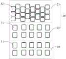
图2是图1所示的显示基板中子像素排布的一种局部示意图;FIG. 2 is a partial schematic diagram of the arrangement of sub-pixels in the display substrate shown in FIG. 1;
图3为图1所示的显示基板中子像素排布的另一种局部示意图;FIG. 3 is another partial schematic diagram of the sub-pixel arrangement in the display substrate shown in FIG. 1;
图4为图1所示的显示基板的局部剖视图;FIG. 4 is a partial cross-sectional view of the display substrate shown in FIG. 1;
图5为图1所示的显示基板中第一显示区内器件在衬底上的局部投影图;FIG. 5 is a partial projection view of the device in the first display area in the display substrate shown in FIG. 1 on the substrate;
图6是图1所示的显示基板中第一显示区的第一电极在衬底上的一种投影示意图;6 is a schematic diagram of a projection of the first electrode of the first display area in the display substrate shown in FIG. 1 on the substrate;
图7是图1所示的显示基板中第一显示区的第一电极在衬底上的另一种投影示意图;FIG. 7 is another schematic projection view of the first electrode of the first display area in the display substrate shown in FIG. 1 on the substrate;
图8是图1所示的显示基板中第一显示区的第一电极在衬底上的再一种投影示意图;FIG. 8 is another schematic projection view of the first electrode of the first display area in the display substrate shown in FIG. 1 on the substrate;
图9是图1所示的显示基板中第一显示区内器件在衬底上的局部投影图;FIG. 9 is a partial projection view of the device in the first display area in the display substrate shown in FIG. 1 on the substrate;
图10是本申请实施例提供的显示装置的设备本体的结构示意图。FIG. 10 is a schematic structural diagram of a device body of a display device provided by an embodiment of the present application.
具体实施方式Detailed ways
这里将详细地对示例性实施例进行说明,其示例表示在附图中。下面的描述涉及附图时,除非另有表示,不同附图中的相同数字表示相同或相似的要素。以下示例性实施例中所描述的实施方式并不代表与本申请相一致的所有实施方式。相反,它们仅是与如所附权利要求书中所详述的、本申请的一些方面相一致的装置的例子。Exemplary embodiments will be described in detail herein, examples of which are illustrated in the accompanying drawings. Where the following description refers to the drawings, the same numerals in different drawings refer to the same or similar elements unless otherwise indicated. The implementations described in the illustrative examples below are not intended to represent all implementations consistent with this application. Rather, they are merely examples of means consistent with some aspects of the present application as recited in the appended claims.
在诸如手机和平板电脑等智能电子设备上,由于需要集成诸如前置摄像头、光线感应器等感光器件,一般是通过在上述电子设备上设置透明显示区的方式,将感光器件设置在透明显示区下方,在保证感光器件正常工作的情况下来实现电子设备的全面屏显示。On smart electronic devices such as mobile phones and tablet computers, due to the need to integrate photosensitive devices such as front cameras and light sensors, the photosensitive devices are generally set in the transparent display area by setting a transparent display area on the above-mentioned electronic devices. Below, the full-screen display of the electronic device is realized under the condition of ensuring the normal operation of the photosensitive device.
但是,电子设备在显示时,会出现透明显示区温度较高,或者透明显示区的像素无法正常工作的问题。发明人研究发现,出现这种问题的原因在于,为了提高透明显示区的透光率,透明显示区内的器件例如子像素的阳极及走线一般采用透明氧化物材料,透明显示区内的像素电路设置在非透明显示区,透明显示区内子像素的阳极通过走线与对应的像素电路电连接。透明氧化物材料的电阻率较高,透明显示区内子像素的阳极与走线之间的接触阻抗较大,会使得透明显示区工作过程中产生的热量较大,从而使得透明显示区的温度较高,可能会影响电子设备的正常工作,甚至会导致阳极与走线无法有效电连接,进而导致透明显示区的子像素无法正常显示的问题。However, when the electronic device is displayed, the temperature of the transparent display area is relatively high, or the pixels in the transparent display area cannot work normally. The inventor found that the reason for this problem is that, in order to improve the light transmittance of the transparent display area, the devices in the transparent display area, such as the anode and the wiring of the sub-pixels, generally use transparent oxide materials, and the pixels in the transparent display area are generally made of transparent oxide materials. The circuit is arranged in the non-transparent display area, and the anodes of the sub-pixels in the transparent display area are electrically connected with the corresponding pixel circuits through wirings. The resistivity of the transparent oxide material is high, and the contact resistance between the anodes of the sub-pixels and the traces in the transparent display area is large, which will cause the heat generated during the operation of the transparent display area to be large, so that the temperature of the transparent display area is higher. High, it may affect the normal operation of electronic equipment, and even cause the anode and the wiring to be unable to be effectively electrically connected, and then cause the problem that the sub-pixels in the transparent display area cannot be displayed normally.
为解决上述问题,本申请实施例提供了一种显示基板、显示面板及显示装置,其能够很好的解决上述问题。In order to solve the above problems, the embodiments of the present application provide a display substrate, a display panel and a display device, which can well solve the above problems.
下面结合附图,对本申请实施例中的显示基板、显示面板及显示装置进行详细说明。在不冲突的情况下,下述的实施例及实施方式中的特征可以相互补充或相互组合。The display substrate, the display panel and the display device in the embodiments of the present application will be described in detail below with reference to the accompanying drawings. Features in the embodiments and implementations described below may complement each other or be combined with each other without conflict.
图1是本申请实施例提供的一种显示基板的俯视图;图2是图1所示的显示基板中子像素排布的一种局部示意图;图3为图1所示的显示基板中子像素排布的另一种局部示意图;图4为图1所示的显示基板的局部剖视图;图5为图1所示的显示基板中第一显示区内器件在衬底上的局部投影图;图6是图1所示的显示基板中第一显示区的第一电极在衬底上的一种投影示意图;图7是图1所示的显示基板中第一显示区的第一电极在衬底上的另一种投影示意图;图8是图1所示的显示基板中第一显示区的第一电极在衬底上的再一种投影示意图;图9是图1所示的显示基板中第一显示区内器件在衬底上的局部投影图;图10是本申请实施例提供的显示装置的设备本体的结构示意图。1 is a top view of a display substrate provided by an embodiment of the present application; FIG. 2 is a partial schematic diagram of the arrangement of sub-pixels in the display substrate shown in FIG. 1 ; FIG. 3 is a sub-pixel in the display substrate shown in FIG. 1 . Another partial schematic diagram of the arrangement; Fig. 4 is a partial cross-sectional view of the display substrate shown in Fig. 1; Fig. 5 is a partial projection view of the device in the first display area in the display substrate shown in Fig. 1 on the substrate; Fig. 6 is a schematic diagram of a projection of the first electrode of the first display area in the display substrate shown in FIG. 1 on the substrate; FIG. 7 is the first electrode of the first display area in the display substrate shown in FIG. 1 on the substrate. Another schematic diagram of projection on the substrate; FIG. 8 is another schematic diagram of projection of the first electrode of the first display area in the display substrate shown in FIG. 1 on the substrate; FIG. 9 is the first electrode in the display substrate shown in FIG. 1. A partial projection view of a device in a display area on a substrate; FIG. 10 is a schematic structural diagram of a device body of a display device provided by an embodiment of the present application.
本申请实施例提供了一种显示基板。参见图1,所述显示基板100包括第一显示区10和第二显示区20,所述第一显示区10的透光率大于所述第二显示区20的透光率。Embodiments of the present application provide a display substrate. Referring to FIG. 1 , the
参见图2或图3,所述第一显示区10内设有多个第一子像素11。参见图4,所述第一子像素11包括第一电极111、设置在所述第一电极111上的发光结构(未图示)及设置在所述发光结构上的第二电极(未图示),用于驱动所述第一子像素11的像素电路设置在所述第二显示区20内,所述第一子像素11的第一电极111通过走线112与对应的像素电路电连接。所述走线112包括互相连接的第一段1121和第二段1122,所述第一段1121位于所述第一显示区10,所述第二段1122位于所述第二显示区20。所述第一显示区10内还设置有导电层113,所述第一电极111通过所述导电层113与所述走线112的第一段1121电连接,所述导电层113的电阻率分别小于所述第一电极111的电阻率及所述第一段1121的电阻率。Referring to FIG. 2 or FIG. 3 , the
本申请实施例提供的显示基板100,由于第一显示区10的透光率大于第二显示区20的透光率,则可将感光器件设置在第一显示区10下方,在保证感光器件正常工作的前提下实现显示基板100的全面屏显示。由于第一显示区10内的第一子像素11的像素电路设置在第二显示区20内,可降低第一显示区10的结构复杂度,进而可减弱外部光线通过第一显示区10时产生的衍射效应,从而可提高第一显示区10下方设置的摄像头的成像质量。通过设置第一电极111通过导电层113与走线112的第一段1121电连接,也即是第一电极111与走线112的第一段1121不直接接触,且导电层113的电阻率分别小于第一电极111与第一段1121的电阻率,则可降低第一显示区10内器件的接触阻抗,从而可降低第一显示区10产生的热量,进而降低显示基板100的温度,保证显示基板100正常工作。In the
在一个实施例中,第一子像素11对应的像素电路可为1T电路、或2T1C电路、或3T1C电路、或7T1C电路或7T2C电路。第二显示区20内的子像素对应的像素电路可为2T1C电路、3T1C电路、或7T1C电路、或7T2C电路。其中,T代表晶体管,C代表存储电容。第一子像素11对应的像素电路、第二显示区20内的子像素对应的像素电路的类型可相同,也可不同。In one embodiment, the pixel circuit corresponding to the
参见图4,所述第二显示区20内的子像素包可括第三电极311、位于所述第三电极311上的发光结构(未图示)及位于发光结构上的第四电极(未图示)。其中第一电极111和第三电极311可为阳极,第二电极和第四电极可为阴极,且第二电极和第四电极可为连成一片的面电极。Referring to FIG. 4 , the sub-pixels in the
再次参见图4,显示基板100还可包括衬底41、位于衬底41上的缓冲层42、形成于缓冲层42上的半导体层36和半导体层14、形成于半导体层36和半导体层14上的栅极绝缘层43、位于栅极绝缘层43上方的电容绝缘层44、位于电容绝缘层44上方的层间介质层45、位于层间介质层45上方的平坦化层46、位于平坦化层上46上的像素限定层47。Referring again to FIG. 4 , the
第一子像素11的像素电路可包括第一晶体管13。第一晶体管13包括漏极131、源极132和栅极133,栅极133位于栅极绝缘层43和电容绝缘层44之间,源极132和漏极131位于层间介质层45上且通过栅极绝缘层43、电容绝缘层44和层间介质层45上的通孔与半导体层14接触。第一电极111位于平坦化层46与像素限定层47之间,且部分被像素限定层47上的像素开口暴露。其中,图4仅以第一子像素11的像素电路包括第一晶体管13(也即是,第一子像素11的像素电路为1T电路)为例进行示意,当然,第一子像素11的像素电路中的晶体管的数量可多于一个,第一子像素11的像素电路还可包括电容。The pixel circuit of the
第二显示区20内子像素的像素电路可包括第二晶体管35和第二电容,第二晶体管35包括源极351、漏极352和栅极353,栅极353位于栅极绝缘层43和电容绝缘层44之间,源极351和漏极352位于层间介质层45上且通过栅极绝缘层43、电容绝缘层44和层间介质层45上的通孔与半导体层36接触。第二电容包括上极板371和下极板372,上极板371位于电容绝缘层44和层间介质层45之间,下极板372位于栅极绝缘层43和电容绝缘层44之间,第三电极311位于平坦化层46与像素限定层47之间。The pixel circuit of the sub-pixels in the
在一个实施例中,再次参见图4,所述第一电极111位于所述导电层113和所述走线112的第一段1121上方,所述第一电极111与所述第一段1121之间设置有第一绝缘层。参见图5所述第一绝缘层上设置有通孔101,所述第一电极111通过所述通孔101与所述导电层113接触。In one embodiment, referring to FIG. 4 again, the
进一步地,所述导电层113与所述第一晶体管13的漏极131可在同一工艺步骤中形成。如此设置,通过一个工艺步骤可同时形成导电层113与第一晶体管13的漏极131,从而可降低显示基板100的制备工艺复杂度。在该情况下,第一电极111与第一段1121之间的绝缘层可为平坦化层46。在其他实施例中,导电层113也可不与第一晶体管13的漏极131同时形成,例如可以在第一晶体管13的漏极131形成之后形成,或者在第一晶体管13的漏极131形成之前形成。Further, the
进一步地,所述走线112的第一段1121与所述导电层113可搭接。如此设置,走线112的第一段1121与所述导电层113位于同一层,无需在绝缘层上设置通孔来实现走线112的第一段1121与导电层113的连接,可进一步简化制备工艺。Further, the
进一步地,走线112的第二段1122与第一晶体管13的漏极131可在同一工艺步骤中形成,以进一步简化制备工艺。Further, the
在一个实施例中,所述第一电极111和/或所述第一段1121的透光率可大于70%。更优选的,第一电极111和/或走线112的第一段1121的透光率可大于或等于90%,例如第一电极111和/或走线112的第一段1121的透光率可以为90%、95%等。如此设置可使得第一显示区10的透光率较大,进而使得第一显示区10的透光率满足其下方设置的感光器件的采光需求。In one embodiment, the light transmittance of the
在一个实施例中,所述第一电极111和/或所述第一段1121的材料可包括氧化铟锡、氧化铟锌、掺杂银的氧化铟锡及掺杂银的氧化铟锌中的至少一种。优选的,制备第一电极111和/或走线112的第一段1121的材料可采用掺杂银的氧化铟锡或者掺杂银的氧化铟锌,以在保证第一显示区10的高透光率的基础上,减小第一电极111和/或走线112的第一段1121的电阻。In one embodiment, the material of the
在一个实施例中,所述导电层113的材料可包括钼、钛、铝、镁、银、金、铜、锌、铬、镍及钨中的至少一种。上述几种材料的电阻率较小,且性质比较稳定。当导电层113与第一晶体管13的漏极131同时制备时,导电层113的材料与第一晶体管13的漏极131可为叠层结构,例如导电层113及第一晶体管13的漏极121可包括两层金属钛膜层及位于两层金属钛膜层之间的金属铝膜层。In one embodiment, the material of the
在一个实施例中,走线112的第一段1121与第二段1122可位于同一层,走线112的第一段1121与第二段1122可搭接。如此设置,便于走线112的第一段1121与第二段1122的连接。In one embodiment, the
在一个实施例中,所述第二电极的材料可包括镁银、氧化铟锡、氧化铟锌、掺杂银的氧化铟锡或者掺杂银的氧化铟锌中的至少一种。其中,镁银是一种包括金属镁和金属银的混合材料。如此设置,第二电极的透光率较高,进而提高第一显示区10的透光率。In one embodiment, the material of the second electrode may include at least one of magnesium silver, indium tin oxide, indium zinc oxide, silver doped indium tin oxide, or silver doped indium zinc oxide. Among them, magnesium silver is a mixed material including metal magnesium and metal silver. In this way, the light transmittance of the second electrode is relatively high, thereby improving the light transmittance of the
在一个实施例中,第一显示区10内设置有多个第一子像素11,每一第一子像素11的第一电极111均通过导电层113与对应的走线112电连接。参见图5,在所述导电层113的延伸方向上,所述导电层113的宽度可连续变化或间断变化,且相邻两个所述导电层113之间的间距可连续变化或间断变化。如此设置,导电层113的不同宽度位置以及相邻导电层113的不同间距之间,产生的衍射条纹的位置不同,不同位置处的衍射效应相互抵消,从而可以有效减弱衍射效应,进而确保设置在第一显示区10下方的摄像头拍照得到的图形具有较高的清晰度。In one embodiment, a plurality of first sub-pixels 11 are disposed in the
进一步地,沿所述导电层113的延伸方向,所述导电层113的边缘可至少部分呈圆弧形或波浪形。通过设置导电层113的边缘呈圆弧形或波浪形,可使得导电层113的宽度连续变化或间断变化,且可使得相邻两个导电层113之间的间距连续变化或间断变化。导电层113的横截面的面积例如可呈圆形、椭圆形等。Further, along the extending direction of the
在一个实施例中,参见图2,所述第二显示区20可包括第一子显示区21以及邻接所述第一子显示区21与所述第一显示区10的第二子显示区22,所述第一子像素11对应的像素电路可设置在所述第二子显示区22内。如此设置,可使得用于连接第一电极111与对应的像素电路的走线112的长度较短,有利于降低显示基板100内走线的复杂度。In one embodiment, referring to FIG. 2 , the
进一步地,所述第二子显示22区内可设置有多个第三子像素31,所述第三子像素31对应的像素电路设置在所述第二子显示区22的靠近所述第一子显示区21的区域内,所述第一子像素11对应的像素电路可设置在所述第二子显示22区的靠近所述第一显示区10的区域内。如此设置,第一子像素11的像素电路和第三子像素31的像素电路在第二子显示区22内位置排布比较合理,可使得第一子像素11的第一电极111与对应的像素电路距离较近,从而使得用于连接第一电极111与对应的像素电路的走线112的长度更短,有利于降低显示基板100内走线的复杂度。Further, a plurality of third sub-pixels 31 may be arranged in the
在一个实施例中,所述第一子显示区21内可设置有多个第二子像素32,所述第一子像素11的密度可与所述第三子像素31的密度相同,且小于第二子像素32的密度。所述第一子像素11的密度与所述第三子像素31的密度相同,可使得第一显示区10与第二子显示区22的显示效果更接近,可在一定程度上降低显示基板100的显示区内像素密度的多样化而造成显示区内各区域显示效果不一致的几率。In one embodiment, a plurality of second sub-pixels 32 may be disposed in the
进一步地,所述第三子像素31的密度可等于所述第二子像素32的密度的一半。通过设置所述第三子像素31的密度等于所述第二子像素32的密度的一半,则第一子像素11的像素电路与第三子像素31的像素电路可各占据第二子显示区22的一半区域,从而使得第一子像素11的像素电路及第三子像素31的像素电路在第二子显示区22中排布更合理。Further, the density of the third sub-pixels 31 may be equal to half of the density of the
进一步地,所述第二子显示区22内相邻的第三子像素31之间的间距大于所述第一子显示区21内相邻的第二子像素32之间的间距,和/或,所述第二子像素32的尺寸小于第三子像素31的尺寸。如此设置,可使得第一子显示区21内第二子像素32的密度大于第二子显示区22内第三子像素31的密度。Further, the spacing between adjacent third sub-pixels 31 in the
在另一个实施例中,参见图3,所述第二显示区20内仅设置有第二子像素32,且第二子像素32可在第二显示区20内均匀分布,也即是第二显示区20内第二子像素32的密度各处相同。In another embodiment, referring to FIG. 3 , only the second sub-pixels 32 are disposed in the
进一步地,第一显示区10内的第一子像素11对应的像素电路设置在第二显示区20的靠近第一显示区10的区域内,以减小走线112的长度,进而降低显示基板100内的走线的复杂度。Further, the pixel circuit corresponding to the
在一个实施例中,每一第一电极111可包括至少一个电极块,设置在第一电极111上的发光结构可包括对应设置在每一电极块上的发光结构块。其中,同一第一电极111的电极块数量为多个时,对应设置在多个电极块上的发光结构块的颜色相同。In one embodiment, each of the
参见图6至图8,当所述第一电极111包括两个或两个以上的电极块1111时,两个或两个以上的电极块1111沿第一方向间隔排布,且该第一电极111还包括设置在相邻两个电极块1111之间的连接部1112,相邻的两个电极块1111通过对应的连接部1112电连接。如此设置,第一电极111中的两个或两个以上的电极块1111可由一个像素电路驱动,从而可减小第一显示区10内的结构的复杂度,能够有效改善光线透射时因第一显示区10的结构复杂而导致的衍射叠加现象,进而提升设置在第一显示区10的背光面设置的摄像头拍摄的图像质量,避免出现图像失真缺陷。并且,同一第一电极111中的多个电极块1111电性连接,从而可控制同一第一电极111的多个电极块1111上对应设置的发光结构块同时发光或同时关闭,可简化对第一显示区10的控制。Referring to FIGS. 6 to 8 , when the
在一个实施例中,所述第一电极111包括两个或两个以上的电极块1111时,所述第一电极111对应的走线112可与该第一电极111的一个电极块1111电连接。由于同一第一电极111中的两个或两个以上的电极块1111电连接,则其中一个电极块1111与对应的走线连接,即可保证该第一电极111的各电极块1111由同一像素电路驱动。In one embodiment, when the
在一个实施例中,所述第一电极111包括两个或两个以上的电极块1111时,所述第一电极111对应的走线112可与该第一电极111的靠近第二子显示区22的电极块1111电连接。如此设置,可进一步减小走线112的第一段1121的长度,有助于进一步降低光线通过第一显示区10时发生的衍射效应。In one embodiment, when the
在一个实施例中,所述显示基板100包括衬底,所述第一电极111位于所述衬底上方,所述电极块1111在所述衬底上的投影可由一个第一图形单元或者多个第一图形单元组成。其中,所述第一图形单元可包括圆形、椭圆形、哑铃形、葫芦形或矩形。In one embodiment, the
图6中所示的第一显示区10中在第一方向上设有一个第一电极111,该第一电极111包括六个电极块1111,每一电极块1111在衬底上的投影由一个第一图形单元组成,该第一图形单元为矩形。图7中所示的第一显示区10中在第一方向上设有一个第一电极111,该第一电极111包括五个电极块1111,每一电极块1111在衬底上的投影由一个第一图形单元组成,该第一图形单元为圆形。图8中所示的第一显示区10中在第一方向上设有两个第一电极111,每一第一电极111包括两个电极块1111,该电极块1111在衬底上的投影由一个第一图形单元组成,该图形单元为哑铃形。第一图形单元为圆形、椭圆形、哑铃形及葫芦形,上述形状可改变衍射产生的周期性结构,即改变了衍射场的分布,从而减弱外部入射光通过时差生的衍射效应。并且,第一图像单元为上述形状时,第一电极在第二方向上的尺寸连续变化或者间断变化,则在第一方向上相邻的两个第一电极在第二方向上的间距连续变化或者间断变化,从而相邻的两个第三电极产生衍射的位置不同,不同位置处的衍射效应相互抵消,从而可以有效减弱衍射效应,进而确保第一显示区下方设置的摄像头拍照得到的图像具有较高的清晰度。The
在一个实施例中,参见图6和图7,在第二方向上,同一第一电极111的多个电极块1111中,相邻的两个电极块1111错位排布,第一方向可与第二方向垂直。如此设置可进一步减弱外部入射的光线通过第一显示区时产生的衍射效应。In one embodiment, referring to FIG. 6 and FIG. 7 , in the second direction, among the plurality of
在一个实施例中,参见图6和图7,同一第一电极111的两个以上的电极块1111中,间隔一个电极块1111设置的两个电极块1111在所述第一方向上的中轴线重合。如此设置可使电极块1111的排布更规则,从而对应设置在多个电极块1111上方的发光结构块的排布更规则,进而制备发光结构块采用的掩模板的开口排布比较规则。在蒸镀第一显示区10和第二显示区20内的发光结构块时,第一显示区10和第二显示区20中的发光结构块可采用同一掩膜板在同一蒸镀工艺中制作,由于掩膜板上的图形较均匀,可减少张网褶皱。In one embodiment, referring to FIG. 6 and FIG. 7 , in the two or
在一个实施例中,所述发光结构块在所述衬底上的投影由一个第二图形单元或者多个第二图形单元组成,所述第二图形单元与所述第一图形单元相同或不同。第一图形单元与第二图像单元不同时,则电极块1111上对应设置的发光结构块在衬底上的投影与该电极块1111在衬底上的投影不同,以进一步减弱光线通过第一显示区10时产生的衍射效应。In one embodiment, the projection of the light-emitting structure block on the substrate is composed of a second graphic unit or a plurality of second graphic units, and the second graphic unit is the same as or different from the first graphic unit . When the first graphic unit is different from the second graphic unit, the projection of the light-emitting structure block correspondingly arranged on the
其中,所述第二图形单元包括圆形、椭圆形、哑铃形、葫芦形或矩形。Wherein, the second graphic unit includes a circle, an ellipse, a dumbbell, a gourd or a rectangle.
在一个实施例中,第一方向与第二方向可互相垂直。其中,第一方向可为行方向,第二方向可为列方向。或者,第一方向可为列方向,第二方向可为行方向。图6至图8中仅以第一方向为行方向,第二方向为列方向为例进行说明,其他情况不再进行图示。In one embodiment, the first direction and the second direction may be perpendicular to each other. The first direction may be a row direction, and the second direction may be a column direction. Alternatively, the first direction may be a column direction, and the second direction may be a row direction. In FIGS. 6 to 8 , only the first direction is the row direction and the second direction is the column direction for illustration, and other situations are not illustrated.
在一个实施例中,所述第一电极111包括两个或两个以上的电极块1111时,同一所述第一电极111的连接部1112与电极块1111可位于同一层。如此设置,电极块1111与连接部1112可在同一工艺步骤中形成,有利于降低工艺复杂度。In one embodiment, when the
进一步地,所述连接部1112在垂直于其延伸方向上的尺寸可大于3μm,且小于所述电极块1111的最大尺寸的二分之一。通过设置连接部1112在垂直于其延伸方向的尺寸大于3μm,可使得连接部1112的电阻较小。通过设置连接部1112的尺寸小于电极块1111的最大尺寸的二分之一,可使得连接部1112的设置对电极块1111的尺寸影响较小,避免连接部1112的尺寸较大导致电极块1111的尺寸减小,进而导致第一显示区10的有效发光面积减小。Further, the dimension of the connecting
在另一个实施例中,所述第一电极111包括两个或两个以上的电极块1111时,同一所述第一电极111的连接部1112与电极块1111可位于不同层,所述连接部1112与所述电极块1111之间设置有第二绝缘层,该第二绝缘层上设置有接触孔,所述连接1112部通过对应的接触孔与所述电极块1111电连接。如此设置,电极块1111的尺寸可不受连接部1112的影响,从而可将电极块1111的尺寸做得较大,进而使第一显示区10的有效发光面积较大。In another embodiment, when the
进一步地,所述第一子像素11的像素电路可包括电容,所述连接部1112与所述电容的上极板可在同一工艺步骤中形成。如此设置,通过一个工艺步骤可同时形成连接部1112与电容的上极板,有助于降低工艺的复杂度。在该情况下,电极块1111与连接部1112之间的第二绝缘层包括层间介质层45和平坦化层46。当然,在其他实施例中,连接部1112也可不与电容的上极板在同一工艺步骤中形成,例如可在电容的上极板形成之前或者形成之后形成。连接部1112的材料也可为透明导电材料,例如氧化铟锡、氧化铟锌、掺杂银的氧化铟锡或者掺杂银的氧化铟锌等。Further, the pixel circuit of the
进一步地,参见图4和图9,像素限定层4上设置有像素开口471,发光结构块115一一对应地设置在所述像素开口471内,第二绝缘层上设置的接触孔48与所述像素开口471之间的距离d的范围可为4μm~30μm。第一子像素11的有效发光面积为像素开口471的开口面积,若连接部1112位于像素开口471的下方,会导致接触孔48处的电极块1111部分凹陷,进而导致发光结构块115进入到凹陷中而造成发光结构块115产生凹陷、降质、点缺陷等问题,因而会降低显示基板的显示质量。通过设置接触孔48的边缘与像素开口471的边缘之间的距离为4μm~30μm,也即是接触孔48不位于像素开口471下方,则可避免像素开口471下方的电极块1111产生凹陷,进而可避免发光结构块115产生凹陷、降质、点缺陷等问题,可保证显示基板的显示质量。Further, referring to FIG. 4 and FIG. 9 ,
其中,接触孔48的边缘与像素开口471的边缘之间的距离指的是接触孔48与像素开口471的相邻的边缘之间的最小距离。The distance between the edge of the
进一步地,接触孔48与所述像素开口471之间的距离d的范围可为4μm~8μm。通过设置接触孔48的边缘与像素开口471的边缘之间的距离d大于4μm,可避免由于工艺误差而导致在像素限定层47上形成像素开口471时发生偏移,而使得形成于接触孔48之上的像素开口471位于接触孔48上方。通过设置接触孔48的边缘与像素开口471的边缘之间的距离d小于8μm,可减小距离d的设置对第一显示区10的有效发光面积的影响。Further, the distance d between the
在一个实施例中,再次参见图9,所述连接部1112可包括第三段1113和多个与所述第三段1113连接的第四段1114,所述第三段1113可沿所述第一方向延伸,所述第四段1114沿第二方向延伸,且多个所述第四段1114在所述第一方向上间隔排布,所述第三段1113和所述第四段1114呈弧形或呈波浪形。In one embodiment, referring to FIG. 9 again, the connecting
其中,第三段1113用于连接多个第四段1114,第四段1114用于通过接触孔48与对应的电极块1111连接。通过第三段1113与第四段1114,可将同一第一电极111的多个电极块1111电连接。The
通过设置第三段1113和第四段1114呈弧形或波浪形,可减小外部光线入射第一显示区10时产生的衍射强度。By arranging the
在一个实施例中,第四段1114可呈弧形,且第四段1114可环绕像素开口471设置。进一步地,像素开口471的横截面可呈圆形,第四段1114可呈圆弧形,且第四段1114及像素开口471在衬底上的投影的圆心可不重合,从而可降低外部光线入射第一显示区10时产生的衍射效应。当然,在其他实施例中,第四段1114与像素开口471在衬底上的投影的圆心也可重合。In one embodiment, the
本申请实施例还提供了一种显示基板,所述显示基板包括第一显示区和第二显示区,所述第一显示区的透光率大于所述第二显示区的透光率。An embodiment of the present application further provides a display substrate, the display substrate includes a first display area and a second display area, and the light transmittance of the first display area is greater than the light transmittance of the second display area.
所述第一显示区内设有多个第一子像素,所述第一子像素包括第一电极、设置在所述第一电极上的发光结构及设置在所述发光结构上的第二电极。参见图9,所述第一电极包括两个或两个以上的电极块1111和至少一个连接部1112,相邻的两个电极块1111通过连接部1112电连接,所述发光结构块包括对应设置在每一电极块上的发光结构块。A plurality of first sub-pixels are arranged in the first display area, and the first sub-pixels include a first electrode, a light-emitting structure arranged on the first electrode, and a second electrode arranged on the light-emitting structure . Referring to FIG. 9 , the first electrode includes two or
同一所述第一电极的连接部1112与电极块1111位于不同层,所述连接部1112与所述电极块1111之间设置有绝缘层,所述绝缘层上设置有接触孔48,所述连接部1112通过对应的接触孔48与所述电极块1111电连接。所述显示基板还包括设置在所述第一电极上的像素限定层,所述像素限定层上设置有像素开口471,所述发光结构块一一对应地设置在所述像素开口471内,所述接触孔48的边缘与所述像素开口471的边缘之间的距离范围为4μm~30μm。The connecting
其中,接触孔48的边缘与像素开口471的边缘之间的距离指的是接触孔48与像素开口471的相邻的边缘之间的最小距离。The distance between the edge of the
本申请实施例提供的显示基板,通过设置接触孔48的边缘与像素开口471的边缘之间的距离为4μm~30μm,也即是接触孔48不位于像素开口471下方,则可避免像素开口471下方的电极块1111产生凹陷,进而可避免发光结构块115产生凹陷、降质、点缺陷等问题,可保证显示基板的显示质量。In the display substrate provided by the embodiment of the present application, by setting the distance between the edge of the
进一步地,所述接触孔48的边缘与所述像素开口471的边缘之间的距离范围为4μm~8μm。通过设置接触孔48的边缘与像素开口471的边缘之间的距离d大于4μm,可避免由于工艺误差而导致在像素限定层47上形成像素开口471时发生偏移,而使得形成于接触孔48之上的像素开口471位于接触孔48上方。通过设置接触孔48的边缘与像素开口471的边缘之间的距离d小于8μm,可减小距离d的设置对第一显示区10的有效发光面积的影响。Further, the distance between the edge of the
其中,本申请实施例中显示基板的结构可以与上述的显示基板100的相关结构相同,具体细节详见上述的实施例,不再进行赘述。The structure of the display substrate in the embodiment of the present application may be the same as the related structure of the above-mentioned
本申请实施例提供的显示基板100的第一显示区10可呈水滴形、圆形、矩形、半圆形、半椭圆形或椭圆形等形状。但不限于此,也可根据实际情况将第一显示区设计为其他形状。The
本申请实施例还提供了一种显示面板,所述显示面板包括上述任一实施例所述的显示基板及封装层。封装层设置在显示基板的背离衬底的一侧。An embodiment of the present application further provides a display panel, where the display panel includes the display substrate and the encapsulation layer described in any of the foregoing embodiments. The encapsulation layer is disposed on a side of the display substrate facing away from the substrate.
封装层可包括偏光片,偏光片可覆盖第二显示区20,或者偏光片可覆盖第二显示区20和第一显示区10。偏光片可消散显示面板表面的反射光,改善用户的使用体验。The encapsulation layer may include a polarizer, and the polarizer may cover the
偏光片未覆盖第一显示区10时,第一显示区10下方可设置透过第一显示区10发射或者采集光线的感光器件。第一显示区10不设置偏光片时,可提高第一显示区10的透光率,保证第一显示区10下方设置的感光器件的正常工作。When the polarizer does not cover the
本申请实施例提供的显示面板,由于第一显示区的透光率大于第二显示区的透光率,则可将感光器件设置在第一显示区下方,在保证感光器件正常工作的前提下实现显示基板的全面屏显示。由于第一显示区内的第一子像素的像素电路设置在第二显示区内,可降低第一显示区的结构复杂度,进而可减弱外部光线通过第一显示区时产生的衍射效应,因而可提高第一显示区下方设置的摄像头的成像质量。通过设置第一电极通过导电层与走线的第一段电连接,也即是第一电极与走线的第一段不直接接触,且导电层的电阻率分别小于第一电极与第一段的电阻率,则可降低第一显示区内器件的接触阻抗,从而可降低第一显示区产生的热量,进而降低显示面板的温度,保证显示面板正常工作。In the display panel provided by the embodiment of the present application, since the light transmittance of the first display area is greater than that of the second display area, the photosensitive device can be arranged under the first display area, on the premise of ensuring the normal operation of the photosensitive device Realize the full screen display of the display substrate. Since the pixel circuit of the first sub-pixel in the first display area is arranged in the second display area, the structural complexity of the first display area can be reduced, and the diffraction effect generated when the external light passes through the first display area can be reduced. The imaging quality of the camera disposed below the first display area can be improved. By setting the first electrode to be electrically connected to the first segment of the trace through the conductive layer, that is, the first electrode is not in direct contact with the first segment of the trace, and the resistivity of the conductive layer is smaller than that of the first electrode and the first segment, respectively. If the resistivity is high, the contact resistance of the device in the first display area can be reduced, thereby reducing the heat generated in the first display area, thereby reducing the temperature of the display panel and ensuring the normal operation of the display panel.
本申请实施例还提供了一种显示装置,显示装置包括设备本体及上述的显示面板。参见图10,设备本体310具有器件区320,显示面板覆盖在设备本体310上。其中,器件区310位于第一显示区10下方,且器件区320中设置有透过第一显示区10进行光线采集的感光器件330。Embodiments of the present application further provide a display device, which includes a device body and the above-mentioned display panel. Referring to FIG. 10 , the
其中,感光器件可包括摄像头和/或光线感应器。器件区中还可设置除感光器件的其他器件,例如陀螺仪或听筒等器件。器件区可以是开槽区,显示面板的第一显示区可对应于开槽区贴合设置,以使得感光器件能够透过该第一显示区进行发射或者采集光线。Wherein, the photosensitive device may include a camera and/or a light sensor. Other devices other than the photosensitive device, such as a gyroscope or an earpiece, can also be arranged in the device area. The device area may be a slotted area, and the first display area of the display panel may be attached to the slotted area, so that the photosensitive device can transmit or collect light through the first display area.
上述显示装置可以为手机、平板、掌上电脑、ipod等数码设备。The above-mentioned display device may be a digital device such as a mobile phone, a tablet, a palmtop computer, and an iPod.
本申请实施例提供的显示装置,由于第一显示区的透光率大于第二显示区的透光率,则可将感光器件设置在第一显示区下方,在保证感光器件正常工作的前提下实现显示基板的全面屏显示。由于第一显示区内的第一子像素的像素电路设置在第二显示区内,可降低第一显示区的结构复杂度,进而可减弱外部光线通过第一显示区时产生的衍射效应,因而可提高第一显示区下方设置的摄像头的成像质量。通过设置第一电极通过导电层与走线的第一段电连接,也即是第一电极与走线的第一段不直接接触,且导电层的电阻率分别小于第一电极与第一段的电阻率,则可降低第一显示区内器件的接触阻抗,从而可降低第一显示区产生的热量,进而降低显示基板的温度,保证显示基板正常工作。In the display device provided by the embodiment of the present application, since the light transmittance of the first display area is greater than that of the second display area, the photosensitive device can be arranged below the first display area, and on the premise of ensuring the normal operation of the photosensitive device Realize the full screen display of the display substrate. Since the pixel circuit of the first sub-pixel in the first display area is arranged in the second display area, the structural complexity of the first display area can be reduced, and the diffraction effect generated when the external light passes through the first display area can be reduced. The imaging quality of the camera disposed below the first display area can be improved. By setting the first electrode to be electrically connected to the first segment of the trace through the conductive layer, that is, the first electrode is not in direct contact with the first segment of the trace, and the resistivity of the conductive layer is smaller than that of the first electrode and the first segment, respectively. If the resistivity is high, the contact resistance of the device in the first display area can be reduced, thereby reducing the heat generated in the first display area, thereby reducing the temperature of the display substrate and ensuring the normal operation of the display substrate.
需要指出的是,在附图中,为了图示的清晰可能夸大了层和区域的尺寸。而且可以理解,当元件或层被称为在另一元件或层“上”时,它可以直接在其他元件上,或者可以存在中间的层。另外,可以理解,当元件或层被称为在另一元件或层“下”时,它可以直接在其他元件下,或者可以存在一个以上的中间的层或元件。另外,还可以理解,当层或元件被称为在两层或两个元件“之间”时,它可以为两层或两个元件之间唯一的层,或还可以存在一个以上的中间层或元件。通篇相似的参考标记指示相似的元件。It should be noted that, in the drawings, the sizes of layers and regions may be exaggerated for clarity of illustration. It will also be understood that when an element or layer is referred to as being "on" another element or layer, it can be directly on the other element or intervening layers may be present. In addition, it will be understood that when an element or layer is referred to as being "under" another element or layer, it can be directly under the other element, or more than one intervening layer or element may be present. In addition, it will also be understood that when a layer or element is referred to as being 'between' two layers or elements, it can be the only layer between the two layers or elements, or more than one intervening layer may also be present or element. Like reference numerals indicate like elements throughout.
在本发明中,术语“第一”、“第二”仅用于描述目的,而不能理解为指示或暗示相对重要性。术语“多个”指两个或两个以上,除非另有明确的限定。In the present invention, the terms "first" and "second" are used for descriptive purposes only, and cannot be understood as indicating or implying relative importance. The term "plurality" refers to two or more, unless expressly limited otherwise.
本领域技术人员在考虑说明书及实践这里公开的公开后,将容易想到本发明的其它实施方案。本发明旨在涵盖本发明的任何变型、用途或者适应性变化,这些变型、用途或者适应性变化遵循本发明的一般性原理并包括本发明未公开的本技术领域中的公知常识或惯用技术手段。说明书和实施例仅被视为示例性的,本发明的真正范围和精神由下面的权利要求指出。Other embodiments of the invention will readily suggest themselves to those skilled in the art upon consideration of the specification and practice of the disclosure disclosed herein. The present invention is intended to cover any variations, uses or adaptations of the present invention which follow the general principles of the present invention and include common knowledge or conventional techniques in the technical field not disclosed by the present invention . The specification and examples are to be regarded as exemplary only, with the true scope and spirit of the invention being indicated by the following claims.
应当理解的是,本发明并不局限于上面已经描述并在附图中示出的精确结构,并且可以在不脱离其范围进行各种修改和改变。本发明的范围仅由所附的权利要求来限制。It should be understood that the present invention is not limited to the precise structures described above and illustrated in the accompanying drawings, and that various modifications and changes may be made without departing from its scope. The scope of the present invention is limited only by the appended claims.
Claims (34)
Translated fromChinesePriority Applications (7)
| Application Number | Priority Date | Filing Date | Title |
|---|---|---|---|
| CN201910580310.8ACN110189639B (en) | 2019-06-28 | 2019-06-28 | Display substrate, display panel and display device |
| PCT/CN2020/072274WO2020258862A1 (en) | 2019-06-28 | 2020-01-15 | Display substrate, display panel, and display device |
| EP20832259.4AEP3992954A4 (en) | 2019-06-28 | 2020-01-15 | DISPLAY SUBSTRATE, DISPLAY PANEL AND DISPLAY DEVICE |
| KR1020217027217AKR102672109B1 (en) | 2019-06-28 | 2020-01-15 | Display substrates, display panels and display devices |
| JP2021551822AJP7213367B2 (en) | 2019-06-28 | 2020-01-15 | Display substrate, display panel, and display device |
| TW109103725ATWI726605B (en) | 2019-06-28 | 2020-02-06 | Display substrate, display panel and display device |
| US17/361,818US20210327958A1 (en) | 2019-06-28 | 2021-06-29 | Display substrate, display panel and display device |
Applications Claiming Priority (1)
| Application Number | Priority Date | Filing Date | Title |
|---|---|---|---|
| CN201910580310.8ACN110189639B (en) | 2019-06-28 | 2019-06-28 | Display substrate, display panel and display device |
Publications (2)
| Publication Number | Publication Date |
|---|---|
| CN110189639A CN110189639A (en) | 2019-08-30 |
| CN110189639Btrue CN110189639B (en) | 2020-12-04 |
Family
ID=67724353
Family Applications (1)
| Application Number | Title | Priority Date | Filing Date |
|---|---|---|---|
| CN201910580310.8AActiveCN110189639B (en) | 2019-06-28 | 2019-06-28 | Display substrate, display panel and display device |
Country Status (7)
| Country | Link |
|---|---|
| US (1) | US20210327958A1 (en) |
| EP (1) | EP3992954A4 (en) |
| JP (1) | JP7213367B2 (en) |
| KR (1) | KR102672109B1 (en) |
| CN (1) | CN110189639B (en) |
| TW (1) | TWI726605B (en) |
| WO (1) | WO2020258862A1 (en) |
Families Citing this family (74)
| Publication number | Priority date | Publication date | Assignee | Title |
|---|---|---|---|---|
| CN110767139B (en)* | 2019-03-29 | 2020-12-11 | 昆山国显光电有限公司 | Display substrate, display panel and display device |
| CN210052743U (en)* | 2019-06-28 | 2020-02-11 | 昆山国显光电有限公司 | Display substrate, display panel and display device |
| CN110189639B (en)* | 2019-06-28 | 2020-12-04 | 昆山国显光电有限公司 | Display substrate, display panel and display device |
| CN110503911B (en)* | 2019-08-09 | 2025-02-28 | 武汉华星光电半导体显示技术有限公司 | Display panel and electronic equipment |
| CN115148780B (en) | 2019-08-27 | 2025-07-15 | 武汉天马微电子有限公司 | Display panel and display device |
| CN110783484B (en)* | 2019-09-24 | 2020-11-10 | 昆山国显光电有限公司 | Display panel, manufacturing method thereof and display device |
| CN210516000U (en) | 2019-09-26 | 2020-05-12 | 昆山国显光电有限公司 | Display substrate and display device |
| CN210516181U (en)* | 2019-09-29 | 2020-05-12 | 昆山国显光电有限公司 | Transparent display substrate and display device |
| WO2021070236A1 (en)* | 2019-10-08 | 2021-04-15 | シャープ株式会社 | Light-emitting device |
| CN110783386B (en)* | 2019-10-29 | 2020-12-25 | 昆山国显光电有限公司 | Display panel and display device |
| JP7329688B2 (en) | 2019-10-31 | 2023-08-18 | オッポ広東移動通信有限公司 | Display devices and electronic devices |
| CN110728921B (en)* | 2019-10-31 | 2022-01-07 | Oppo广东移动通信有限公司 | Display device and electronic apparatus |
| EP4044167A4 (en)* | 2019-10-31 | 2022-11-23 | Guangdong Oppo Mobile Telecommunications Corp., Ltd. | DISPLAY DEVICE AND ELECTRONIC DEVICE |
| CN110648622A (en)* | 2019-10-31 | 2020-01-03 | Oppo广东移动通信有限公司 | Display devices and electronic equipment |
| CN114144827B (en) | 2019-10-31 | 2023-09-22 | Oppo广东移动通信有限公司 | Display devices and electronic equipment |
| CN110599944B (en)* | 2019-10-31 | 2024-10-11 | Oppo广东移动通信有限公司 | Display device and electronic equipment |
| CN110619837A (en)* | 2019-10-31 | 2019-12-27 | Oppo广东移动通信有限公司 | Display device and electronic apparatus |
| CN117098422A (en)* | 2019-11-07 | 2023-11-21 | 华为技术有限公司 | Display panel and electronic equipment |
| CN110729337A (en)* | 2019-11-15 | 2020-01-24 | 京东方科技集团股份有限公司 | Display substrate, method for making the same, and electronic device |
| CN210515985U (en)* | 2019-11-21 | 2020-05-12 | 昆山国显光电有限公司 | Display substrate, display panel and display device |
| CN115347033A (en) | 2019-11-27 | 2022-11-15 | 武汉天马微电子有限公司 | A display panel and a display device |
| CN110783394A (en)* | 2019-11-28 | 2020-02-11 | 昆山国显光电有限公司 | Light-transmitting display panel, display panel and display device |
| CN111312755B (en) | 2019-11-29 | 2021-06-08 | 昆山国显光电有限公司 | Display panel and display device |
| CN112599577B (en)* | 2019-12-03 | 2023-03-21 | Oppo广东移动通信有限公司 | Display screen assembly and electronic device |
| KR20210070466A (en)* | 2019-12-04 | 2021-06-15 | 삼성디스플레이 주식회사 | Electronic device with display portion |
| CN110890026B (en)* | 2019-12-05 | 2021-10-15 | 昆山国显光电有限公司 | Display panel and display device |
| CN111029382A (en)* | 2019-12-13 | 2020-04-17 | 合肥维信诺科技有限公司 | Display panel, multi-area display panel and display device |
| CN111063719B (en)* | 2019-12-30 | 2022-08-12 | 武汉天马微电子有限公司 | Display panel and display device |
| CN111048005B (en)* | 2020-01-06 | 2021-06-22 | 昆山国显光电有限公司 | Display panel and display device |
| CN111833720B (en) | 2020-01-13 | 2021-08-31 | 昆山国显光电有限公司 | A display panel and display device |
| WO2021147082A1 (en)* | 2020-01-23 | 2021-07-29 | 京东方科技集团股份有限公司 | Display substrate and preparation method therefor |
| JP7482900B2 (en)* | 2020-01-23 | 2024-05-14 | 京東方科技集團股▲ふん▼有限公司 | Display substrate and manufacturing method thereof |
| CN111326560B (en)* | 2020-01-23 | 2023-08-22 | 京东方科技集团股份有限公司 | Display substrate and display device |
| CN113345929B (en)* | 2020-02-18 | 2023-07-18 | 京东方科技集团股份有限公司 | Display substrate, manufacturing method thereof, and display device |
| CN111834400B (en)* | 2020-02-26 | 2021-10-12 | 昆山国显光电有限公司 | Display panel, manufacturing method thereof and display device |
| CN111341936B (en) | 2020-03-10 | 2021-11-12 | 昆山国显光电有限公司 | Display panel and display device |
| CN113496971A (en)* | 2020-04-08 | 2021-10-12 | 北京芯海视界三维科技有限公司 | Terminal connection structure, display unit and display |
| CN111834413A (en)* | 2020-04-17 | 2020-10-27 | 昆山国显光电有限公司 | Display panel and display device |
| CN111508416B (en)* | 2020-04-30 | 2021-09-03 | 武汉华星光电半导体显示技术有限公司 | Display and driving method thereof |
| CN111584569B (en)* | 2020-05-13 | 2024-02-06 | 武汉华星光电半导体显示技术有限公司 | Display panel and display device |
| EP4156277A4 (en) | 2020-06-08 | 2023-11-15 | Guangdong Oppo Mobile Telecommunications Corp., Ltd. | Display device, processing method therefor, and electronic device |
| CN111584609A (en)* | 2020-06-08 | 2020-08-25 | Oppo广东移动通信有限公司 | Display device, manufacturing method of display device and electronic equipment |
| CN113838888B (en)* | 2020-06-23 | 2024-10-22 | 京东方科技集团股份有限公司 | Display substrate and display device |
| CN111725287A (en)* | 2020-06-30 | 2020-09-29 | 武汉天马微电子有限公司 | Display panel, display device and manufacturing method of display panel |
| CN111816112B (en)* | 2020-07-24 | 2022-04-08 | 昆山国显光电有限公司 | Method and device for determining compensation parameters of display panel |
| CN115843201A (en)* | 2020-08-07 | 2023-03-24 | 武汉天马微电子有限公司 | Display panel and display device |
| CN112038374B (en)* | 2020-09-02 | 2023-04-18 | 昆山国显光电有限公司 | Display panel and display device |
| CN112116872B (en)* | 2020-09-23 | 2022-12-06 | 京东方科技集团股份有限公司 | Display panel, manufacturing method thereof, and display device |
| US12336384B2 (en)* | 2020-09-29 | 2025-06-17 | Chengdu Boe Optoelectronics Technology Co., Ltd. | Display panel and display apparatus |
| KR20220046054A (en) | 2020-10-06 | 2022-04-14 | 삼성디스플레이 주식회사 | Display panel and display apparatus including the same |
| CN114373784A (en)* | 2020-10-14 | 2022-04-19 | Oppo广东移动通信有限公司 | Display devices and electronic equipment |
| CN112271268A (en)* | 2020-11-05 | 2021-01-26 | 武汉华星光电半导体显示技术有限公司 | Display panel and display device |
| CN114447032A (en)* | 2020-11-05 | 2022-05-06 | 云谷(固安)科技有限公司 | Display panel and display device |
| CN114822250B (en)* | 2020-12-28 | 2023-06-06 | 武汉天马微电子有限公司 | A display panel and a display device |
| TWI770750B (en)* | 2020-12-31 | 2022-07-11 | 友達光電股份有限公司 | Pixel array substrate |
| CN113161374B (en)* | 2021-03-17 | 2022-11-25 | 上海和辉光电股份有限公司 | Display panel of under-screen camera and preparation method |
| BR112023020305A2 (en) | 2021-04-05 | 2023-11-21 | Samsung Electronics Co Ltd | ELECTRONIC DEVICE CONTAINING CAMERA MODULE |
| CN113096581B (en)* | 2021-04-16 | 2022-09-20 | 武汉天马微电子有限公司 | Display panel and display device |
| KR20220159550A (en)* | 2021-05-25 | 2022-12-05 | 삼성디스플레이 주식회사 | Display module, and electronic device including the same |
| KR20220165875A (en)* | 2021-06-08 | 2022-12-16 | 삼성디스플레이 주식회사 | Display device and electronic device having the same |
| TWI784612B (en)* | 2021-07-05 | 2022-11-21 | 友達光電股份有限公司 | Display device |
| KR20230041119A (en) | 2021-09-16 | 2023-03-24 | 삼성디스플레이 주식회사 | Display device and tiled display device including the same |
| CN216623636U (en)* | 2021-12-15 | 2022-05-27 | 昆山国显光电有限公司 | Display panel and display device |
| CN114283691B (en)* | 2021-12-31 | 2025-08-26 | 厦门天马显示科技有限公司 | Display panel and display device including the same |
| EP4340024A4 (en)* | 2022-01-30 | 2024-11-20 | BOE Technology Group Co., Ltd. | DISPLAY BOARD AND MANUFACTURING METHOD THEREFOR AND DISPLAY DEVICE |
| CN114512522B (en)* | 2022-02-10 | 2024-07-05 | 厦门天马显示科技有限公司 | Display panel and display device |
| CN114779955B (en)* | 2022-04-01 | 2025-05-13 | Tcl华星光电技术有限公司 | Touch panel and touch display device |
| CN114783292B (en)* | 2022-04-20 | 2023-11-10 | 京东方科技集团股份有限公司 | Display substrate and display device |
| CN117337630A (en)* | 2022-04-27 | 2024-01-02 | 京东方科技集团股份有限公司 | Display panels and display devices |
| CN114975570A (en)* | 2022-06-24 | 2022-08-30 | 昆山国显光电有限公司 | Display panel and display device |
| CN117438430A (en)* | 2022-07-12 | 2024-01-23 | 京东方科技集团股份有限公司 | Display substrate and display device |
| KR20240108067A (en)* | 2022-12-30 | 2024-07-09 | 엘지디스플레이 주식회사 | Display device |
| WO2024147178A1 (en)* | 2023-01-05 | 2024-07-11 | シャープディスプレイテクノロジー株式会社 | Display device |
| CN119008803A (en)* | 2024-07-03 | 2024-11-22 | 京东方华灿光电(苏州)有限公司 | LED for improving bonding pad damage and preparation method thereof |
Citations (9)
| Publication number | Priority date | Publication date | Assignee | Title |
|---|---|---|---|---|
| CN104282724A (en)* | 2013-07-08 | 2015-01-14 | 三星显示有限公司 | Organic light emitting display devices and methods of manufacturing organic light emitting display devices |
| CN105702205A (en)* | 2016-04-19 | 2016-06-22 | 天马微电子股份有限公司 | Display panel and display device |
| CN108376696A (en)* | 2017-09-30 | 2018-08-07 | 云谷(固安)科技有限公司 | Terminal and display screen |
| CN109273481A (en)* | 2017-07-17 | 2019-01-25 | 上海和辉光电有限公司 | A kind of display panel and display device |
| US20190066545A1 (en)* | 2017-08-28 | 2019-02-28 | Lg Display Co., Ltd. | Flexible color filter substrate and flexible light emitting display apparatus including the same |
| CN208608202U (en)* | 2018-08-06 | 2019-03-15 | 云谷(固安)科技有限公司 | Display panel, display screen and display terminal |
| CN109600459A (en)* | 2017-09-30 | 2019-04-09 | 云谷(固安)科技有限公司 | Electric terminal and display screen |
| CN109728046A (en)* | 2018-12-29 | 2019-05-07 | 上海天马有机发光显示技术有限公司 | A kind of display panel and display device |
| CN208861990U (en)* | 2018-10-31 | 2019-05-14 | 昆山维信诺科技有限公司 | Display screen and display terminal |
Family Cites Families (21)
| Publication number | Priority date | Publication date | Assignee | Title |
|---|---|---|---|---|
| JP4663257B2 (en)* | 2003-06-16 | 2011-04-06 | 株式会社半導体エネルギー研究所 | Light emitting device and manufacturing method thereof |
| JP2010230797A (en)* | 2009-03-26 | 2010-10-14 | Seiko Epson Corp | Display device and electronic device |
| KR101746198B1 (en)* | 2009-09-04 | 2017-06-12 | 가부시키가이샤 한도오따이 에네루기 켄큐쇼 | Display device and electronic device |
| KR102680781B1 (en)* | 2012-12-25 | 2024-07-04 | 가부시키가이샤 한도오따이 에네루기 켄큐쇼 | Semiconductor device |
| WO2015060203A1 (en)* | 2013-10-22 | 2015-04-30 | Semiconductor Energy Laboratory Co., Ltd. | Display device |
| KR102261610B1 (en)* | 2014-07-30 | 2021-06-08 | 삼성디스플레이 주식회사 | Organic light emitting display device |
| WO2016042638A1 (en)* | 2014-09-18 | 2016-03-24 | パイオニア株式会社 | Light emitting device |
| KR102540372B1 (en)* | 2015-05-28 | 2023-06-05 | 엘지디스플레이 주식회사 | Organic light emitting display device and method of manufacturing the same |
| KR102654924B1 (en)* | 2016-06-16 | 2024-04-05 | 삼성디스플레이 주식회사 | Display apparatus |
| US10319935B2 (en)* | 2017-04-05 | 2019-06-11 | Joled Inc. | Organic EL display panel and method of manufacturing organic EL display panel |
| CN107133613B (en)* | 2017-06-06 | 2020-06-30 | 上海天马微电子有限公司 | A display panel and display device |
| CN108257514A (en)* | 2017-09-30 | 2018-07-06 | 昆山国显光电有限公司 | Display screen, display panel drive method and its display device |
| WO2019062236A1 (en)* | 2017-09-30 | 2019-04-04 | 昆山国显光电有限公司 | Display screen, display screen driving method and display device thereof |
| CN114256322B (en)* | 2018-06-28 | 2025-04-01 | 厦门天马微电子有限公司 | Organic light emitting display panel, display device and display method thereof |
| CN208622778U (en)* | 2018-08-06 | 2019-03-19 | 云谷(固安)科技有限公司 | Display panel, display screen and display terminal |
| KR102643092B1 (en)* | 2018-10-02 | 2024-03-06 | 삼성디스플레이 주식회사 | Fingerprint sensor and display device including the same |
| CN109256047B (en)* | 2018-10-31 | 2021-12-17 | 武汉天马微电子有限公司 | Display panel, display device and driving method thereof |
| CN109410823B (en)* | 2018-12-27 | 2022-04-19 | 厦门天马微电子有限公司 | Display panel and display device |
| CN109801950B (en)* | 2019-01-31 | 2021-02-26 | 厦门天马微电子有限公司 | Display panel, display device and manufacturing method of display panel |
| CN109859647B (en)* | 2019-03-29 | 2022-04-08 | 上海天马微电子有限公司 | Display panel and display device |
| CN110189639B (en)* | 2019-06-28 | 2020-12-04 | 昆山国显光电有限公司 | Display substrate, display panel and display device |
- 2019
- 2019-06-28CNCN201910580310.8Apatent/CN110189639B/enactiveActive
- 2020
- 2020-01-15KRKR1020217027217Apatent/KR102672109B1/enactiveActive
- 2020-01-15JPJP2021551822Apatent/JP7213367B2/enactiveActive
- 2020-01-15WOPCT/CN2020/072274patent/WO2020258862A1/ennot_activeCeased
- 2020-01-15EPEP20832259.4Apatent/EP3992954A4/enactivePending
- 2020-02-06TWTW109103725Apatent/TWI726605B/enactive
- 2021
- 2021-06-29USUS17/361,818patent/US20210327958A1/enactivePending
Patent Citations (9)
| Publication number | Priority date | Publication date | Assignee | Title |
|---|---|---|---|---|
| CN104282724A (en)* | 2013-07-08 | 2015-01-14 | 三星显示有限公司 | Organic light emitting display devices and methods of manufacturing organic light emitting display devices |
| CN105702205A (en)* | 2016-04-19 | 2016-06-22 | 天马微电子股份有限公司 | Display panel and display device |
| CN109273481A (en)* | 2017-07-17 | 2019-01-25 | 上海和辉光电有限公司 | A kind of display panel and display device |
| US20190066545A1 (en)* | 2017-08-28 | 2019-02-28 | Lg Display Co., Ltd. | Flexible color filter substrate and flexible light emitting display apparatus including the same |
| CN108376696A (en)* | 2017-09-30 | 2018-08-07 | 云谷(固安)科技有限公司 | Terminal and display screen |
| CN109600459A (en)* | 2017-09-30 | 2019-04-09 | 云谷(固安)科技有限公司 | Electric terminal and display screen |
| CN208608202U (en)* | 2018-08-06 | 2019-03-15 | 云谷(固安)科技有限公司 | Display panel, display screen and display terminal |
| CN208861990U (en)* | 2018-10-31 | 2019-05-14 | 昆山维信诺科技有限公司 | Display screen and display terminal |
| CN109728046A (en)* | 2018-12-29 | 2019-05-07 | 上海天马有机发光显示技术有限公司 | A kind of display panel and display device |
Also Published As
| Publication number | Publication date |
|---|---|
| EP3992954A4 (en) | 2022-12-21 |
| JP7213367B2 (en) | 2023-01-26 |
| TW202025116A (en) | 2020-07-01 |
| TWI726605B (en) | 2021-05-01 |
| KR102672109B1 (en) | 2024-06-05 |
| KR20210113401A (en) | 2021-09-15 |
| EP3992954A1 (en) | 2022-05-04 |
| JP2022522493A (en) | 2022-04-19 |
| US20210327958A1 (en) | 2021-10-21 |
| CN110189639A (en) | 2019-08-30 |
| WO2020258862A1 (en) | 2020-12-30 |
Similar Documents
| Publication | Publication Date | Title |
|---|---|---|
| CN110189639B (en) | Display substrate, display panel and display device | |
| CN210052743U (en) | Display substrate, display panel and display device | |
| CN110767720B (en) | Display substrate, display panel and display device | |
| US11968873B2 (en) | Display substrate and display device | |
| CN110767662B (en) | Display substrate, display panel and display device | |
| TWI698689B (en) | Display panel | |
| CN110767835B (en) | Transparent display panel, display screen, display device and mask plate | |
| CN110764362B (en) | Mask strip, array substrate, display screen and display device | |
| US11864432B2 (en) | Display substrate, display panel and display apparatus | |
| WO2021057012A1 (en) | Light-transmitting display panel and manufacturing method therefor, display panel and manufacturing method therefor, and display device | |
| CN111029382A (en) | Display panel, multi-area display panel and display device | |
| CN106910765A (en) | A kind of electroluminescence display panel, its preparation method and display device | |
| WO2020087799A1 (en) | Display screen and display terminal | |
| WO2020087804A1 (en) | Display panel, display screen, and display terminal | |
| WO2020087820A1 (en) | Display screen and display terminal | |
| TW201939733A (en) | Array substrate, display panel, and display device | |
| CN210516728U (en) | Display substrate, display panel and display device | |
| WO2020133938A1 (en) | Display panel, display panel manufacturing method, display screen, and display terminal | |
| CN113728296B (en) | Touch substrate and touch display device | |
| CN118946208B (en) | Display panel and display device |
Legal Events
| Date | Code | Title | Description |
|---|---|---|---|
| PB01 | Publication | ||
| PB01 | Publication | ||
| SE01 | Entry into force of request for substantive examination | ||
| SE01 | Entry into force of request for substantive examination | ||
| GR01 | Patent grant | ||
| GR01 | Patent grant |