CN110147177B - Display device - Google Patents
Display deviceDownload PDFInfo
- Publication number
- CN110147177B CN110147177BCN201910414391.4ACN201910414391ACN110147177BCN 110147177 BCN110147177 BCN 110147177BCN 201910414391 ACN201910414391 ACN 201910414391ACN 110147177 BCN110147177 BCN 110147177B
- Authority
- CN
- China
- Prior art keywords
- signal
- circuit
- drive
- supplied
- drive electrode
- Prior art date
- Legal status (The legal status is an assumption and is not a legal conclusion. Google has not performed a legal analysis and makes no representation as to the accuracy of the status listed.)
- Active
Links
Images


Classifications
- G—PHYSICS
- G09—EDUCATION; CRYPTOGRAPHY; DISPLAY; ADVERTISING; SEALS
- G09G—ARRANGEMENTS OR CIRCUITS FOR CONTROL OF INDICATING DEVICES USING STATIC MEANS TO PRESENT VARIABLE INFORMATION
- G09G3/00—Control arrangements or circuits, of interest only in connection with visual indicators other than cathode-ray tubes
- G09G3/20—Control arrangements or circuits, of interest only in connection with visual indicators other than cathode-ray tubes for presentation of an assembly of a number of characters, e.g. a page, by composing the assembly by combination of individual elements arranged in a matrix no fixed position being assigned to or needed to be assigned to the individual characters or partial characters
- G09G3/34—Control arrangements or circuits, of interest only in connection with visual indicators other than cathode-ray tubes for presentation of an assembly of a number of characters, e.g. a page, by composing the assembly by combination of individual elements arranged in a matrix no fixed position being assigned to or needed to be assigned to the individual characters or partial characters by control of light from an independent source
- G09G3/36—Control arrangements or circuits, of interest only in connection with visual indicators other than cathode-ray tubes for presentation of an assembly of a number of characters, e.g. a page, by composing the assembly by combination of individual elements arranged in a matrix no fixed position being assigned to or needed to be assigned to the individual characters or partial characters by control of light from an independent source using liquid crystals
- G09G3/3611—Control of matrices with row and column drivers
- G09G3/3648—Control of matrices with row and column drivers using an active matrix
- G09G3/3655—Details of drivers for counter electrodes, e.g. common electrodes for pixel capacitors or supplementary storage capacitors
- G—PHYSICS
- G06—COMPUTING OR CALCULATING; COUNTING
- G06F—ELECTRIC DIGITAL DATA PROCESSING
- G06F3/00—Input arrangements for transferring data to be processed into a form capable of being handled by the computer; Output arrangements for transferring data from processing unit to output unit, e.g. interface arrangements
- G06F3/01—Input arrangements or combined input and output arrangements for interaction between user and computer
- G06F3/03—Arrangements for converting the position or the displacement of a member into a coded form
- G06F3/041—Digitisers, e.g. for touch screens or touch pads, characterised by the transducing means
- G06F3/0412—Digitisers structurally integrated in a display
- G—PHYSICS
- G06—COMPUTING OR CALCULATING; COUNTING
- G06F—ELECTRIC DIGITAL DATA PROCESSING
- G06F3/00—Input arrangements for transferring data to be processed into a form capable of being handled by the computer; Output arrangements for transferring data from processing unit to output unit, e.g. interface arrangements
- G06F3/01—Input arrangements or combined input and output arrangements for interaction between user and computer
- G06F3/03—Arrangements for converting the position or the displacement of a member into a coded form
- G06F3/041—Digitisers, e.g. for touch screens or touch pads, characterised by the transducing means
- G06F3/044—Digitisers, e.g. for touch screens or touch pads, characterised by the transducing means by capacitive means
- G06F3/0443—Digitisers, e.g. for touch screens or touch pads, characterised by the transducing means by capacitive means using a single layer of sensing electrodes
- G—PHYSICS
- G09—EDUCATION; CRYPTOGRAPHY; DISPLAY; ADVERTISING; SEALS
- G09G—ARRANGEMENTS OR CIRCUITS FOR CONTROL OF INDICATING DEVICES USING STATIC MEANS TO PRESENT VARIABLE INFORMATION
- G09G2300/00—Aspects of the constitution of display devices
- G09G2300/04—Structural and physical details of display devices
- G09G2300/0421—Structural details of the set of electrodes
- G09G2300/0426—Layout of electrodes and connections
- G—PHYSICS
- G09—EDUCATION; CRYPTOGRAPHY; DISPLAY; ADVERTISING; SEALS
- G09G—ARRANGEMENTS OR CIRCUITS FOR CONTROL OF INDICATING DEVICES USING STATIC MEANS TO PRESENT VARIABLE INFORMATION
- G09G3/00—Control arrangements or circuits, of interest only in connection with visual indicators other than cathode-ray tubes
- G09G3/20—Control arrangements or circuits, of interest only in connection with visual indicators other than cathode-ray tubes for presentation of an assembly of a number of characters, e.g. a page, by composing the assembly by combination of individual elements arranged in a matrix no fixed position being assigned to or needed to be assigned to the individual characters or partial characters
- G09G3/34—Control arrangements or circuits, of interest only in connection with visual indicators other than cathode-ray tubes for presentation of an assembly of a number of characters, e.g. a page, by composing the assembly by combination of individual elements arranged in a matrix no fixed position being assigned to or needed to be assigned to the individual characters or partial characters by control of light from an independent source
- G09G3/36—Control arrangements or circuits, of interest only in connection with visual indicators other than cathode-ray tubes for presentation of an assembly of a number of characters, e.g. a page, by composing the assembly by combination of individual elements arranged in a matrix no fixed position being assigned to or needed to be assigned to the individual characters or partial characters by control of light from an independent source using liquid crystals
- G09G3/3611—Control of matrices with row and column drivers
- G09G3/3648—Control of matrices with row and column drivers using an active matrix
Landscapes
- Engineering & Computer Science (AREA)
- Theoretical Computer Science (AREA)
- General Engineering & Computer Science (AREA)
- Physics & Mathematics (AREA)
- General Physics & Mathematics (AREA)
- Human Computer Interaction (AREA)
- Computer Hardware Design (AREA)
- Chemical & Material Sciences (AREA)
- Crystallography & Structural Chemistry (AREA)
- Power Engineering (AREA)
- Liquid Crystal (AREA)
- Control Of Indicators Other Than Cathode Ray Tubes (AREA)
- Liquid Crystal Display Device Control (AREA)
- Position Input By Displaying (AREA)
- Devices For Indicating Variable Information By Combining Individual Elements (AREA)
Abstract
Translated fromChinese
Description
Translated fromChinese本申请是申请日为2016年03月04日、申请号为201610125420.1、发明名称为“显示装置”的专利申请的分案申请,其全部内容结合于此作为参考。This application is a divisional application of a patent application with an application date of March 4, 2016, an application number of 201610125420.1, and an invention title of "display device", the entire contents of which are incorporated herein by reference.
技术领域technical field
本发明涉及显示装置,尤其涉及能够检测外部接近物体的带触摸检测功能的显示装置。The present invention relates to a display device, and more particularly, to a display device with a touch detection function capable of detecting an external approaching object.
背景技术Background technique
近年来,被称为触摸面板的能够检测外部接近物体的触摸检测装置备受关注。触摸面板安装在显示装置例如液晶显示装置上、或与液晶显示装置一体化。这样,触摸面板安装在显示装置上或被一体化的显示装置、即带触摸检测功能的显示装置使显示装置显示各种按钮图像等,通过触摸面板检测外部物体接近按钮图像。由此,将触摸面板作为一般的机械式按钮的代替,能够作为信息输入单元使用。由于这样的带触摸检测功能的显示装置不再必备键盘、鼠标那样的信息输入单元,除计算机之外,即使是移动电话那样的便携式信息终端等也存在扩大使用的趋势。In recent years, a touch detection device called a touch panel capable of detecting an approaching external object has attracted attention. The touch panel is mounted on or integrated with a display device such as a liquid crystal display device. In this way, a touch panel is mounted on or integrated with a display device, that is, a display device with a touch detection function displays various button images on the display device, and the touch panel detects the approach of an external object to the button images. Thereby, the touch panel can be used as an information input unit instead of a general mechanical button. Since such a display device with a touch detection function no longer requires an information input unit such as a keyboard and a mouse, the use of portable information terminals such as mobile phones in addition to computers tends to expand.
作为触摸检测装置的检测方式,存在光学式、电阻式、静电电容式等几种方式。其中,静电电容式的触摸检测装置具有比较简单的构造且耗电低,因此,正在被使用于便携式信息终端等。在专利文献1中,记载有静电电容式的触摸检测装置。As the detection method of the touch detection device, there are several methods, such as an optical type, a resistive type, and an electrostatic capacitance type. Among them, an electrostatic capacitance type touch detection device has a relatively simple structure and low power consumption, and therefore, is being used in portable information terminals and the like. In
此外,在显示装置中,越来越追求显示面的大型化。与此相应,也追求触摸面板的大型化。另一方面,由于显示装置自身的大型化不利于可移动性而不期待。因此,为了抑制显示装置大型化的同时实现显示面的大型化,追求显示装置的边框窄化。即,追求围着显示装置的显示面的边框的窄化。In addition, in display devices, an increase in the size of the display surface has been increasingly pursued. Correspondingly, an increase in the size of the touch panel is also pursued. On the other hand, since the size of the display device itself is not good for portability, it is not expected. Therefore, in order to realize the enlargement of the display surface while suppressing the enlargement of the display device, the bezel of the display device has been demanded to be narrowed. That is, narrowing of the frame surrounding the display surface of the display device is pursued.
【在先技术 文献】【Prior Art Literature】
【专利文献】【Patent Literature】
专利文献1:日本特开2012-230657号公报Patent Document 1: Japanese Patent Laid-Open No. 2012-230657
在静电电容式的触摸检测装置中,例如专利文献1所示的那样,利用由于手指等外部物体接近(包括接触)驱动电极和检测电极交叉的交叉部分的容量值变化,检测外部物体的接近。即,当向驱动电极供给驱动信号时,根据检测电极产生的检测信号,检测外部物体的接近。在触摸检测装置中,分别设置多个这样的驱动电极和检测电极,多个驱动电极沿列方向依次配置,多个检测电极以与多个驱动电极交叉的方式沿行方向依次配置。In an electrostatic capacitance type touch detection device, as disclosed in
形成驱动信号的电路形成在相当于边框的区域。为了实现边框窄化,若相当于边缘的区域窄化,则分配形成驱动信号电路的区域变窄,降低电路的驱动能力。若驱动能力降低,则驱动电极的电压变化延迟,有可能涉及触摸检测的特性恶化。A circuit for forming a drive signal is formed in an area corresponding to the frame. In order to realize the narrowing of the frame, if the area corresponding to the edge is narrowed, the area allocated to form the driving signal circuit is narrowed, and the driving capability of the circuit is reduced. When the driving capability is lowered, the voltage change of the driving electrodes is delayed, and there is a possibility that the characteristics related to touch detection may be deteriorated.
发明内容SUMMARY OF THE INVENTION
本发明的目的在于提供抑制边框增加并能够防止触摸检测特性恶化的带触摸检测功能的显示装置。An object of the present invention is to provide a display device with a touch detection function capable of suppressing an increase in bezel and preventing deterioration of touch detection characteristics.
本发明的一个方面涉及的显示装置具备:像素阵列,包括配置成矩阵状的多个像素,具有与行平行的第一边和与第一边相对的第二边;多条扫描线,配置在像素阵列的各行,向在对应的行配置的多个像素供给扫描信号;多条信号线,配置在像素阵列的各列,向在对应的列配置的多个像素供给图像信号;多个驱动电极,配置在像素阵列的列,被供给用于检测外部接近物体的驱动信号;以及第一驱动电极电路,沿着像素阵列的第一边配置,与配置于像素阵列的多条控制线和多个驱动电极连接,向多个驱动电极中的、通过经由多条控制线供给的选择信号所指定的驱动电极供给驱动信号。A display device according to an aspect of the present invention includes: a pixel array including a plurality of pixels arranged in a matrix, having a first side parallel to a row and a second side opposite to the first side; a plurality of scanning lines arranged in Each row of the pixel array supplies a scan signal to a plurality of pixels arranged in a corresponding row; a plurality of signal lines are arranged in each column of the pixel array, and supply an image signal to a plurality of pixels arranged in a corresponding column; a plurality of driving electrodes , arranged in a column of the pixel array, and supplied with a drive signal for detecting an external approaching object; and a first drive electrode circuit, arranged along the first side of the pixel array, and arranged in the pixel array with a plurality of control lines and a plurality of The drive electrodes are connected, and a drive signal is supplied to a drive electrode designated by a selection signal supplied through a plurality of control lines among the plurality of drive electrodes.
附图说明Description of drawings
图1是示出实施方式一涉及的带触摸检测功能的液晶显示装置的构成的框图。FIG. 1 is a block diagram showing the configuration of a liquid crystal display device with a touch detection function according to the first embodiment.
图2的(A)~(C)是用于说明静电电容型触摸检测(互电容式) 的基本原理的说明图。(A) to (C) of FIG. 2 are explanatory diagrams for explaining the basic principle of electrostatic capacitance type touch detection (mutual capacitance type).
图3的(A)和(B)是示出安装了实施方式一涉及的带触摸检测功能的液晶显示装置的模块的概要俯视图以及截面图。(A) and (B) of FIG. 3 are a schematic plan view and a cross-sectional view showing a module on which the liquid crystal display device with a touch detection function according to the first embodiment is mounted.
图4的(A)~(C)是示出安装了实施方式一涉及的带触摸检测功能的液晶显示装置的模块的概概要俯视图以及截面图。(A) to (C) of FIG. 4 are a schematic plan view and a cross-sectional view showing a module on which the liquid crystal display device with a touch detection function according to the first embodiment is mounted.
图5是示出安装了实施方式一涉及的带触摸检测功能的液晶显示装置的模块构成的俯视图。5 is a plan view showing a module configuration in which the liquid crystal display device with a touch detection function according to the first embodiment is mounted.
图6是示出实施方式一涉及的像素阵列的构成的电路图。6 is a circuit diagram showing the configuration of the pixel array according to the first embodiment.
图7是示出实施方式一涉及的带触摸检测功能的液晶显示装置的构成的框图。7 is a block diagram showing the configuration of the liquid crystal display device with a touch detection function according to the first embodiment.
图8是示出实施方式一涉及的带触摸检测功能的液晶显示装置的构成的电路图。8 is a circuit diagram showing the configuration of the liquid crystal display device with a touch detection function according to the first embodiment.
图9的(A)~(E)是示出实施方式一涉及的带触摸检测功能的液晶显示装置的动作的波形图。(A) to (E) of FIG. 9 are waveform diagrams showing operations of the liquid crystal display device with a touch detection function according to the first embodiment.
图10是示出实施方式二涉及的带触摸检测功能的液晶显示装置的构成的框图。10 is a block diagram showing a configuration of a liquid crystal display device with a touch detection function according to the second embodiment.
图11是示出实施方式二涉及的带触摸检测功能的液晶显示装置的构成的电路图。11 is a circuit diagram showing a configuration of a liquid crystal display device with a touch detection function according to the second embodiment.
图12的(A)~(E)是示出实施方式二涉及的带触摸检测功能的液晶显示装置的动作的波形图。(A) to (E) of FIG. 12 are waveform diagrams showing operations of the liquid crystal display device with a touch detection function according to the second embodiment.
图13是示出实施方式三涉及的带触摸检测功能液晶显示装置的构成的框图。13 is a block diagram showing a configuration of a liquid crystal display device with a touch detection function according to the third embodiment.
图14是示出实施方式三涉及的带触摸检测功能的液晶显示装置的电路图。14 is a circuit diagram showing a liquid crystal display device with a touch detection function according to Embodiment 3. FIG.
图15的(A)~(E)是示出实施方式三涉及的带触摸检测功能的液晶显示装置的动作的波形图。(A) to (E) of FIG. 15 are waveform diagrams showing operations of the liquid crystal display device with a touch detection function according to the third embodiment.
具体实施方式Detailed ways
下面,参照图说明本发明的各实施方式。此外,公开仅为一例,本领域技术人员在维持发明的主旨的适当变更而容易想到的均包括在本发明的范围内。此外,附图为了更明确地说明,与实际的状态相比,存在将各部分的宽度、厚度、形状等示意性显示的情况,但这到底是一个例子,并不限定本发明的理解。Hereinafter, each embodiment of the present invention will be described with reference to the drawings. In addition, the disclosure is merely an example, and those skilled in the art can easily conceive of changes while maintaining the gist of the invention, and are included in the scope of the present invention. In addition, in the drawings, the width, thickness, shape, etc. of each part may be schematically shown in comparison with the actual state in order to explain more clearly, but this is merely an example and does not limit the understanding of the present invention.
此外,在本说明书和各图中,对于已给图中的与上述物品相同的要素附于相同的符号,并适当省略详细的说明。In addition, in this specification and each drawing, the same code|symbol is attached|subjected to the same element as the above-mentioned thing in the drawing, and a detailed description is abbreviate|omitted suitably.
在以下的说明中,作为带触摸检测功能的显示装置,以带触摸检测功能的液晶显示装置为例叙述。但是,不限定于此,也能够适用于带触摸检测功能OLED显示装置。此外,如上所述,作为触摸检测方式存在多种方式,但在以下的说明中,作为触摸检测方式采用静电电容式为例进行说明。此外,在采用静电电容式的触摸检测方式的触摸检测装置中,由于存在多种方式,在此以使用互电容方式的触摸检测方式的触摸检测装置为例进行说明。In the following description, as a display device with a touch detection function, a liquid crystal display device with a touch detection function will be described as an example. However, it is not limited to this, and can be applied to an OLED display device with a touch detection function. In addition, as described above, there are various methods as a touch detection method, but in the following description, an electrostatic capacitance method is used as an example of a touch detection method. In addition, there are various types of touch detection devices using an electrostatic capacitance type touch detection method, and a touch detection device using a mutual capacitance type touch detection method is described here as an example.
此外,在本说明书中,以把触摸检测装置和显示装置一体化的内置型 (in-cell)的带触摸检测功能的液晶显示装置为适用例进行说明。在此,所谓内置型的带触摸检测功能的液晶显示装置是指触摸检测装置中所包括的驱动电极和检测电极的至少一方设置于经由显示装置的液晶而相对的一对基板间的带触摸检测功能的液晶显示装置。具体来说,以触摸检测装置所包括的驱动电极用作驱动液晶的驱动电极的情况进行说明。驱动电极被共用作触摸检测用的驱动电极和液晶显示用的驱动电极,在以下的说明中,存在将驱动电极称为公共电极的情况。In addition, in this specification, an in-cell liquid crystal display device with a touch detection function in which a touch detection device and a display device are integrated is described as an application example. Here, the built-in-type liquid crystal display device with a touch detection function refers to a touch detection device with at least one of drive electrodes and detection electrodes included in the touch detection device provided between a pair of substrates opposed to each other via liquid crystals of the display device. functional liquid crystal display device. Specifically, the case where the drive electrodes included in the touch detection device are used as drive electrodes for driving liquid crystals will be described. The drive electrodes are commonly used as drive electrodes for touch detection and drive electrodes for liquid crystal display, and in the following description, the drive electrodes are sometimes referred to as common electrodes.
(实施方式一)(Embodiment 1)
<静电电容型触摸检测(互电容式)的基本原理><Basic principle of electrostatic capacitance type touch detection (mutual capacitance type)>
首先,说明互电容方式的基本原理。图2的(A)~(C)是示出后述的实施方式一~三中所采用的静电电容式的触摸检测的基本原理示意图。在图2的(A)中,TL(0)~TL(p)分别是设置于液晶面板的公共电极,RL(0)~RL(p)分别是设置于触摸检测面板部的检测电极。在图2的(A)中,公共电极TL(0)~TL(p)分别沿列向延伸且沿行向平行地配置。另外,检测电极RL(0)~RL(p)分别以与公共电极TL (0)~TL(p)交叉的方式沿行向延伸、沿列向平行地配置。检测电极 RL(0)~RL(p)以在检测电极RL(0)~RL(p)与公共电极TL(0)~ TL(p)之间产生间隙的方式形成在公共电极TL(0)~TL(p)的上方。First, the basic principle of the mutual capacitance method will be described. (A) to (C) of FIG. 2 are schematic diagrams showing the basic principle of capacitive touch detection employed in
在图2的(A)中,12-0~12-p分别示意性表示单位驱动电极驱动器。在同一图中,从单位驱动电极驱动器12-0~12-p输出驱动信号Tx(0)~ Tx(p)。此外,13-0~13-p分别示意性表示单位放大部。在图2的(A) 中,以实线的○圈起来的脉冲信号显示驱动信号Tx(i)的波形。作为外部物体,在同一图中,手指作为FG显示。In (A) of FIG. 2 , 12-0 to 12-p schematically represent unit drive electrode drivers, respectively. In the same figure, drive signals Tx( 0 ) to Tx(p) are output from the unit drive electrode drivers 12 - 0 to 12 -p. In addition, 13-0 to 13-p each schematically represent a unit amplification part. In (A) of FIG. 2 , the waveform of the drive signal Tx(i) is shown by the pulse signal circled by the solid line ○. As an external object, the finger is shown as FG in the same figure.
在图2的例子中,作为来自单位驱动电极驱动器12-2的驱动信号Tx (2),向公共电极TL(2)供给脉冲信号。通过向公共电极TL(2)供给作为脉冲信号的驱动信号Tx(2),从而如图2的(B)所示,在与公用电极TL(2)交叉的检测电极RL(n)之间产生电场。此时,当手指FG正在触摸接近液晶面板的公共电极TL(2)的位置时,在手指FG与公共电极TL(2)之间也产生电场,公共电极TL(2)与检测电极RL(n)之间产生的电场减少。由此,公共电极TL(2)与检测电极RL(n)之间的电荷量减少。其结果,如图2的(C)所示,应答驱动信号Tx(2)的供给产生的电荷量,与手指FG没有触摸时相比,触摸时仅减少ΔQ。电荷量差作为电压差表现为检测信号Rx(n),供给到单位放大部13-n,被放大。In the example of FIG. 2, a pulse signal is supplied to the common electrode TL(2) as the drive signal Tx(2) from the unit drive electrode driver 12-2. By supplying the drive signal Tx( 2 ), which is a pulse signal, to the common electrode TL( 2 ), as shown in FIG. 2(B) , a generation is generated between the detection electrodes RL(n) crossing the common electrode TL( 2 ). electric field. At this time, when the finger FG is touching a position close to the common electrode TL(2) of the liquid crystal panel, an electric field is also generated between the finger FG and the common electrode TL(2), and the common electrode TL(2) and the detection electrode RL(n ) reduces the electric field generated between them. Thereby, the amount of electric charges between the common electrode TL(2) and the detection electrode RL(n) is reduced. As a result, as shown in (C) of FIG. 2 , the amount of charge generated in response to the supply of the drive signal Tx( 2 ) is reduced by ΔQ only when the finger FG is touched, compared to when the finger FG is not touched. The difference in charge amount is expressed as a voltage difference as a detection signal Rx(n), and is supplied to the unit amplifier 13-n and amplified.
另外,在图2的(C)中,横轴表示时间,纵轴表示电荷量。应答于驱动信号Tx(2)电压的上升,电荷量增加(在同一图中向上侧增加),响应于驱动信号Tx(2)的电压的下降,电荷量增加(在同一图中向下侧增加)。此时,通过手指FG触摸的有无,增加的电荷量变化。此外,在该附图中,在电荷量向上侧增加后、向下侧增加前,进行复位,同样地,在电荷量向下侧增加后、向上侧增加前,进行电荷量的复位。通过这种方式,以复位的电荷量为基准,电荷量上下变化。In addition, in FIG. 2(C), the horizontal axis represents time, and the vertical axis represents the amount of electric charge. In response to a rise in the voltage of the drive signal Tx(2), the amount of charge increases (increases to the upper side in the same graph), and in response to a decrease in the voltage of the drive signal Tx(2), the amount of charge increases (increases to the lower side in the same graph ). At this time, the increased charge amount changes depending on whether or not the finger FG is touched. In addition, in this drawing, reset is performed after the charge amount increases upward and before the charge amount increases downward, and similarly, the charge amount is reset after the charge amount increases downward and before the charge amount increases upward. In this way, the charge amount changes up and down based on the reset charge amount.
通过向公共电极TL(0)~TL(p)依次供给驱动信号Tx(0)~Tx (p),从而从与供给驱动信号Tx(i)的公共电极交叉的多个检测电极RL (0)~RL(p)分别输出具有手指FG是否触摸接近于各个交叉部分的位置相应的电压值的检测信号Rx(0)~Rx(p)。在电荷量产生差ΔQ的时刻,对检测信号Rx(0)~Rx(p)中的各个检测信号抽样,使用模拟/数字转换部(以下称为A/D转换部)转换为数字信号。通过对A/D转换部转换的数字信号进行信号处理,抽出被触摸位置的坐标。By sequentially supplying the drive signals Tx(0) to Tx(p) to the common electrodes TL(0) to TL(p), the plurality of detection electrodes RL(0) intersecting with the common electrode to which the drive signal Tx(i) is supplied ˜RL(p) respectively output detection signals Rx(0)˜Rx(p) having voltage values corresponding to whether or not the finger FG touches the positions close to the respective intersections. When the difference in charge amount ΔQ occurs, each of the detection signals Rx(0) to Rx(p) is sampled and converted into a digital signal using an analog/digital converter (hereinafter referred to as an A/D converter). The coordinates of the touched position are extracted by performing signal processing on the digital signal converted by the A/D converter.
<整体构成><Overall composition>
接着,使用图1对带触摸检测功能的液晶显示装置(以下仅称为液晶显示装置)1的整体构成进行说明。图1是示出带触摸检测功能的液晶显示装置1的构成的框图。带触摸检测功能的液晶显示装置1包括液晶面板 (显示面板)2、显示控制装置5、信号线选择器6、触摸控制装置7以及栅极驱动器8。在图1中,为了易于看清附图,示意性画出液晶面板2,包括液晶面板部(显示面板部)3和触摸检测面板部4。将在后文使用图3 和图4对液晶面板2的结构进行说明。Next, the overall configuration of a liquid crystal display device with a touch detection function (hereinafter simply referred to as a liquid crystal display device) 1 will be described with reference to FIG. 1 . FIG. 1 is a block diagram showing the configuration of a liquid
这些液晶面板部3和触摸检测面板部4共用驱动电极。向液晶面板部 3供给来自栅极驱动器8的扫描信号Vs0~Vsp,进一步经由信号线选择器 6供给来自显示控制装置5的图像信号SLd(0)~SLd(p),显示依照图像信号SLd(0)~SLd(p)的图像。触摸检测面板部4供给来自显示控制装置5的驱动信号Tx(0)~Tx(p),并将检测信号Rx(0)~Rx(p) 向触摸控制装置7输出。The liquid crystal panel portion 3 and the touch detection panel portion 4 share drive electrodes. The scanning signals Vs0 to Vsp from the
显示控制装置5具有控制部9和驱动电路10,驱动电路10具有形成并输出图像信号的信号线驱动器11和输出驱动信号Tx(0)~Tx(p)的驱动电极驱动器12。控制部9接收已供给控制端子Tt的定时信号及控制信号和已供给图像端子Td的图像信号,将与已供给图像端子Td的图像信号对应的图像信号Sn供给信号线驱动器11。信号线驱动器11将从控制部 9已供给的图像信号Sn没有特别的限制而在时间上多重化而向信号线选择器6输出。即,当观察到信号线驱动器11的一个输出端子时,两个图像信号在时间上错开的同时从一个端子输出。The
此外,控制部9将在信号线选择器6中用于时间上多重化后的图像信号向彼此不同的信号线分配的选择信号SEL1、SEL2供给信号线选择器6。信号线选择器6根据选择信号SEL1、SEL2将多重化而已供给的图像信号向彼此不同的信号线分配,并作为图像信号SLd(0)~SLd(p)而供给液晶面板部3。信号线选择器6配置在液晶面板部3的附近。这样,通过将图像信号在时间上多重化,能够减少将显示控制装置5与液晶面板部3 电连接的布线的数量。换而言之,能够使连接显示控制装置5与液晶面板部3之间的布线的宽度变宽,进而降低图像信号的延迟。Further, the control unit 9 supplies the
控制部9根据供给到控制端子Tt的定时信号和控制信号,向栅极驱动器8供给定时信号。栅极驱动器8根据已供给的定时信号,产生扫描信号Vs0~Vsp,供给到液晶面板部3。由栅极驱动器8产生的扫描信号Vs0~ Vsp是例如从扫描信号Vs0向着Vsp电平依次变高的脉冲信号。The control unit 9 supplies the
驱动电路10内的驱动电极驱动器12接收由触摸控制装置7供给的选择信号TP(0)~TP(p),向液晶面板2所包括多个公共电极TL(0)~ TL(p)供给驱动信号Tx(0)~Tx(p)。没有特别的限制,但在该实施方式一中,驱动信号Tx(0)~Tx(p)与选择信号TP(0)~TP(p)一对一对应。检测到触摸时,从多个公共电极TL(0)~TL(p)中选择检测触摸的公共电极(以下,可称为选择公共电极)和不检测触摸的公共电极(以下,可称为非选择公共电极)。这个选择由选择信号TP(0)~TP (p)以指定选择公共电极的方式进行。The
例如,当选择信号TP(i)将公共电极TL(i)指定为选择公共电极 TL(i)时,驱动电极驱动器12将与该选择信号TP(i)对应的驱动信号 Tx(i)作为其电压周期性变化的时钟信号输出。此时,例如若选择信号 TP(n)将公共电极TL(n)指定为非选择公共电极,则驱动电极驱动器 12将与该选择信号TP(n)对应的驱动信号Tx(n)固定为规定电压。如使用图2说明的那样,通过公共电极的电压周期性变化这种方式,能够进行该公共电极的附近是否被接触的检测。For example, when the selection signal TP(i) designates the common electrode TL(i) as the selection common electrode TL(i), the
没有特别的限制,但在该实施方式一中,触摸控制装置7依照外部端子Ta所供给的选择信息形成选择信号TP(0)~TP(p)。因此,依照选择信息将任意的公共电极指定为选择公共电极,则能够进行任意的选择公共电极的附近是否被触摸的检测。There is no particular limitation, but in the first embodiment, the
没有特别的限制,但在该实施方式一中,触摸控制装置7依照选择信息,将与选择公共电极对应的选择信号例如定为高电平,将与非选择公共电极对应的选择信号定为低电平。并且,当触摸控制装置7检测触摸时,输出电压周期性变化的控制信号(时钟信号)TSVCOM。驱动电极驱动器 12接收选择信号TP(0)~TP(p)和控制信号TSVCOM,作为与成为高电平的选择信号对应的驱动信号,输出控制信号TSVCOM。此外,作为成为低电平的选择信号对应的驱动信号,输出接地电压。There is no particular limitation, but in the first embodiment, the
该实施方式一涉及的带触摸检测功能的液晶显示装置1为内置型,驱动电极TL(i)被兼用作触摸检测的驱动和液晶的驱动。即,驱动电极TL (i)在显示图像时,发挥将用于驱动液晶的电场形成在后述的像素电极之间的功能,当检测到触摸时,发挥传达触摸检测用驱动信号的功能。液晶面板部3中液晶的图像显示和触摸检测面板部4的触摸检测在时间上不重合地分时进行。即,显示图像的显示期间和进行触摸检测的触摸检测时间不重合地分时产生。The liquid
在进行图像显示的显示期间,驱动电极驱动器12将用于驱动液晶的驱动信号Tx(i)供给液晶面板2内的公共电极TL(i);在进行触摸检测的检测期间,将用于触摸检测的驱动信号Tx(i)供给液晶面板2内的公共电极TL(i)。当然,也可以在驱动电路10中分开设置用于触摸检测的驱动电极驱动器和用于驱动液晶的驱动电极驱动器。另外,控制部9输出识别显示期间和触摸检测期间的触摸-显示同步信号TSHD。During the display period for image display, the
触摸控制装置7包括:处理来自触摸检测面板部4的检测信号Rx(0)~ Rx(p)的检测信号处理部TS;形成向驱动电极驱动器12供给的选择信号TP(0)~TP(p)和控制信号TSVCOM、VCOMSEL、xVCOMSEL 的驱动信号形成部17;控制检测信号处理部TS和驱动信号形成部17的控制部18。在此,检测信号处理部TS检测触摸检测面板部4是否被触摸,被触摸的情况下,进行求得被触摸位置的坐标的处理。此外,驱动信号形成部17进行触摸检测面板部4中检测触摸区域的指定和控制。The
首先,对检测信号处理部TS进行说明,该检测信号处理部TS包括:接收来自触摸检测面板部4的检测信号Rx(0)~Rx(p)并将接收到的检测信号Rx(0)~Rx(p)放大的触摸检测信号放大部13;将由触摸检测信号放大部13放大后的模拟检测信号向数字信号转换的A/D转换部14。在这里,触摸检测信号放大部13从接收到的检测信号Rx(0)~Rx(p) 中去除高频成分(噪声成分),进行放大动作。此外,如使用图2说明的那样,检测信号Rx(0)~Rx(p)应答向公共电极TL(i)供给的驱动信号Tx(i)产生。因此,在该实施方式一中,A/D转换部14与驱动信号 Tx(i)同步,抽样来自触摸检测信号放大部13的放大信号,由控制部18 控制向数字信号转换。First, the detection signal processing unit TS including the detection signals Rx(0) to Rx(p) received from the touch detection panel unit 4 and the received detection signals Rx(0) to Rx(p) will be described. The touch detection
并且,检测信号处理部TS具有:信号处理部15,接收通过A/D转换部14的转换动作得到的数字信号,对该数字信号执行信号处理;以及坐标提取部16,从通过信号处理部15的处理得到的信号中提取已触摸的位置的坐标。作为信号处理部15进行的信号处理,包括除掉比在A/D转换部14进行抽样的频率的高频率噪声成分,并且检测触摸检测面板部4的触摸的有无的处理。由坐标提取部16所提取的已触摸的位置坐标从输出端子Tout作为坐标信息输出。Further, the detection signal processing unit TS includes a
驱动信号形成部17根据来自控制部18的控制信号,形成选择信号 TP(0)~TP(p)和控制信号TSVCOM、VCOMSEL、xVCOMSEL,供给到驱动电极驱动器12。控制部18经由来自显示控制装置5的控制部9 所输出的触摸-显示同步信号TSHD和外部端子Ta接收选择信息,当该触摸-显示同步信号TSHD显示触摸检测期间时,控制驱动信号形成部17形成选择信号TP(0)~TP(p)和控制信号TSVCOM、VCOMSEL、 xVCOMSEL。The drive
即,控制部18控制驱动信号形成部17,以使由选择信息指定的公共电极对应的选择信号成为高电平,其余的选择信号成为低电平。并且,控制部18控制驱动信号形成部17,使驱动信号形成部17在触摸检测期间输出电压周期性变化的控制信号TSVCOM以及在触摸检测期间为高电平的控制信号VCOMSEL。控制信号xVCOMSEL是相对于控制信号 VCOMSEL相位反转了的控制信号。即,在触摸检测期间内,控制信号 xVCOMSEL为低电平。另外,控制部18控制A/D转换部14、信号处理部15以及坐标提取部16,以使在触摸检测期间,其转换触摸检测信号放大部13接收到的检测信号Rx(0)~Rx(p),提取已触摸的坐标。That is, the
<模块><module>
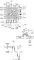
图3的(A)是示出安装了实施方式一的带触摸检测功能的液晶显示装置1的模块概要的俯视图。另外,图3的(B)是图3的(A)中B-B’的截面图。FIG. 3(A) is a plan view showing an outline of a module in which the liquid
液晶面板2具备在图3的(A)中纵向延伸并横向并列配置的信号线 SL(0)~SL(p)以及与这些信号线SL(0)~SL(p)的延伸方向同向延伸的多个公共电极TL(0)~TL(p)。即,公共电极TL(0)~TL(p) 分别在同一图中纵向延伸,横向并列地配置。此外,传达供给扫描信号 Vs0~Vsp的扫描线及检测信号Rx(0)~Rx(p)的检测电极RL(0)~ RL(p)在同一图中横向延伸、纵向并列地配置,但在图3的(A)中省略。The
另外,在图3的(A)中,2-U示出液晶面板2的短边(第一边),2-D 是液晶面板2的边,示出与短边2-U相对的短边(第二边)。并且,2-L 示出液晶面板2的长边,2-R是液晶面板2的边,示出与长边2-L相对的长边。在此,短边2-U、2-D是分别与扫描线以及检测线Rx(0)~Rx(p) 平行的边,长边2-L、2-R是分别与信号线SL(0)~SL(p)以及公共电极TL(0)~TL(p)平行的边。In addition, in FIG. 3(A), 2-U shows the short side (first side) of the
图1说明的显示控制装置5及信号线选择器6沿着液晶面板2的短边 2-D配置。即,显示控制装置5以及信号线选择器6在与信号线SL(0)~ SL(p)以及公共电极TL(0)~TL(p)正交的方向延伸。在后文使用图5进行说明,信号线选择器6与液晶面板2形成于相同的基板,信号线 SL(0)~SL(p)与信号线选择器6连接,从显示控制装置5输出的图像信号经由信号线选择器6供给到液晶面板2的信号线SL(0)~SL(p)。在此,从显示控制装置5供给到信号线选择器6的信号是图像信号和选择信号。液晶面板2为了进行彩色显示,从显示控制装置5供给到信号线选择器6的图像信号是相当于三原色的R(红)、G(绿)、B(青)的图像信号,在同一图中作为R/G/B显示。另外,在该图中,选择信号作为SEL1、SEL2显示。由于信号线选择器6和信号线驱动器11与信号线SL(0)~ SL(p)相关联,可视为信号线电路,该信号线电路可视为沿着液晶面板 2的短边2-D配置。The
信号线SL(0)~SL(p)分别形成于作为玻璃基板的TFT基板300 的一个主面。在图3所示的模块中,多条信号线(例如,信号线SL(0) 0、SL(0)1)对应一个公共电极(例如,公共电极TL(0)),各个信号线SL(0)0、SL(0)1包括对应图像信号R、G、B的三个信号线。图3 的(B)中,示出信号线SL(0)0中包括的图像信号R、G、B对应的信号线SL(0)0(R)、SL(0)0(G)、SL(0)0(B)、以及信号线SL(1) 中包括的图像信号R、G、B对应的信号线SL(1)0(R)、SL(1)0(G)、 SL(1)0(B)。The signal lines SL( 0 ) to SL(p) are respectively formed on one main surface of the
在此,使用本说明书对信号线的标示方法进行说明。以信号线SL(0) 0(R)及信号线SL(1)0(R)为例说明,首先()内的数字示出对应的公共电极的编号,下一个数字示出公共电极的像素数字,()内的字母显示像素三原色(R、G、B)。即,信号线SL(0)0(R)是对应公共电极 TL(0)的信号线,示出传递在第0号像素与三原色的红对应的图像信号的信号线。同样地,信号线SL(1)0(R)是对应与公共电极TL(0)相邻配置的公共电极TL(1)的信号线,示出传递在第0号像素与三原色的红对应的图像信号的信号线。因此,图3的(B)示出的SL(1)1(R) 以及SL(1)1(G)分别为与公共电极TL(1)对应的信号线,表示传递第一号像素的三原色的红以及绿对应图像信号的信号线。Here, the method of marking the signal line will be described using this manual. Taking the signal line SL(0) 0(R) and the signal line SL(1)0(R) as an example, the first number in ( ) shows the number of the corresponding common electrode, and the next number shows the pixel of the common electrode Numbers, letters in ( ) show the three primary colors of pixels (R, G, B). That is, the signal line SL(0)0(R) is a signal line corresponding to the common electrode TL(0), and shows a signal line that transmits an image signal corresponding to the three primary colors of red in the 0th pixel. Similarly, the signal line SL(1)0(R) is a signal line corresponding to the common electrode TL(1) arranged adjacent to the common electrode TL(0), and shows that the signal line SL(1)0(R) corresponding to the three primary colors of red is transmitted in the 0th pixel. Signal lines for image signals. Therefore, SL(1)1(R) and SL(1)1(G) shown in FIG. 3(B) are signal lines corresponding to the common electrode TL(1), respectively, indicating that the three primary colors of the first pixel are transmitted The red and green corresponding to the signal lines of the image signal.
如图3的(B)所示,对应图像信号R、G、B的信号线SL(0)0(R)、 SL(0)0(G)、SL(0)0(B)的一个主面和TFT基板300的一个主面进一步形成有绝缘层301,绝缘层301上形成公共电极TL(0)~TL(p)。这些公共电极TL(0)~TL(p)分别形成辅助电极SM,辅助电极SM电连接于公共电极,降低公共电极的电阻。在公共电极TL(0)~TL(p) 和辅助电极SM的上方的面形成绝缘层302,绝缘层302的上表面形成像素电极LDP。在图3的(B)中,CR、CB、CG分别为滤色片,滤色片 CR(红)、CG(绿)、CB(青)和绝缘层302之间夹着液晶层303。在此,像素电极LDP设置在扫描线和信号线的交点,在各像素电极LDP的上方设置分别与像素电极LDP对应的彩色滤波器CR、CG或CB。各彩色滤波器CR、CG、CB之间设置黑矩阵(Black Matrix)BM。As shown in (B) of FIG. 3 , one main of the signal lines SL(0)0(R), SL(0)0(G), and SL(0)0(B) corresponding to the image signals R, G, B
图4是示出检测电极RL(0)~RL(p)和公共电极TL(0)~TL(p) 关系的示意图。如图4的(A)所示,在彩色滤波器CR、CG、CB的上表面设置为玻璃基板的CF玻璃基板400,在CF玻璃基板400的上表面形成检测电极RL(0)~RL(p)。此外,在检测电极RL(0)~RL(p)的上方形成偏光板401。此外,在此,如图4的(A)所示,由于以同一图中从上方向下观察的情况为例,作为上方的面叙述,但通过观察方向的改变,也可称为上侧的面、下侧的面或侧面的面。另外,在图4的(A)中,检测电极RL(0)~RL(p)和公共电极TL(0)~TL(p)之间形成的电容元件的电极以虚线画出。FIG. 4 is a schematic diagram showing the relationship between the detection electrodes RL(0) to RL(p) and the common electrodes TL(0) to TL(p). As shown in FIG. 4(A) , a
如图3的(A)及图4的(C)所示,信号线SL(0)~SL(p)及公共电极TL(0)~TL(p)分别在纵向,即长边方向延伸,在横向,即短边方向并列配置。与此相对,如图4的(B)所示,检测电极RL(0)~ RL(p)设置于CF玻璃基板400,与公共电极TL(0)~TL(p)交差地配置。即,在图4的(B)中,横向(短边)延伸,纵向(长边)并列地配置。该检测电极RL(0)~RL(p)的各个检测信号Rx(0)~Rx(p) 供给到触摸控制装置7。没有特别的限制,但在该实施方式一中,如图4的(B)所示,检测信号Rx(0)~Rx(p)交替取出。As shown in FIG. 3(A) and FIG. 4(C) , the signal lines SL( 0 ) to SL(p) and the common electrodes TL( 0 ) to TL(p) extend in the longitudinal direction, that is, in the longitudinal direction, respectively. They are arranged side by side in the lateral direction, that is, in the short-side direction. On the other hand, as shown in FIG. 4(B) , the detection electrodes RL(0) to RL(p) are provided on the
俯视观察时,如图3的(A)所示,可将信号线SL(0)~SL(p) 和公共电极TL(0)~TL(p)视为平行延伸。此外,平行是指双方从一端到另一端无交叉地延伸,一条线的一部分或者全部即便以相对于另一条线倾斜的状态设置,如果这两条线从一端到另一端没有交叉,那么这种状态为“平行”。When viewed from above, as shown in FIG. 3(A) , the signal lines SL( 0 ) to SL(p) and the common electrodes TL( 0 ) to TL(p) can be regarded as extending in parallel. In addition, parallel means that both sides extend from one end to the other end without crossing, even if part or all of one line is arranged in a state of being inclined relative to the other line, if the two lines do not cross from one end to the other end, then this kind of The status is "parallel".
另外,以信号线选择器6以及显示控制装置5为基点,掌握公共电极 TL(0)~TL(p)的配置时,公共电极TL(0)~TL(p)分别可视为从作为基点的信号线选择器6及显示控制装置5远离的方向延伸。此时,信号线SL(0)~SL(p)也可视为从作为基点的信号线选择器6以及显示控制装置5远离的方向延伸。In addition, when the arrangement of the common electrodes TL( 0 ) to TL(p) is grasped on the basis of the
另外,在图4的(A)中,省略图3的(B)示出的信号线以及像素电极LDP。In addition, in FIG. 4(A) , the signal lines and the pixel electrodes LDP shown in FIG. 3(B) are omitted.
<模块的整体构成><Overall configuration of the module>
图5是示意性示出实施方式的模块的整体构成的俯视图,显示安装有带触摸检测功能的液晶显示装置1的模块500的整体构成。虽然是示意性示出,但图5配合实际的配置而描绘。FIG. 5 is a plan view schematically showing the overall configuration of the module according to the embodiment, and shows the overall configuration of a
另外,图5不仅示出实施方式一,也显示后文说明的实施方式二及三涉及的模块的整体构成。由于后文详细叙述实施方式二及三的构成部分,此处仅简单叙述。In addition, FIG. 5 shows not only the first embodiment but also the overall configuration of the modules according to the second and third embodiments to be described later. Since the components of the second and third embodiments will be described in detail later, they will only be briefly described here.
在图5中,501显示图3中说明的TFT基板300的区域,502显示具有图4中说明的TFT基板300和CF玻璃基板400的区域。在模块500中, TFT基板300一体地设置。即,在区域501和502中,TFT基板300共用,区域502中,如图4所示,在TFT基板300的上方的面进一步形成CF玻璃基板400、检测电极RL(0)~RL(p)及偏光板401等。In FIG. 5 , 501 shows the region of the
在图5中,500-U示出模块500的短边,500-D是模块500的边,示出与短边500-U相对的短边。并且,500-L示出模块500的长边,500-R 是模块的边,示出与长边500-L相对的长边。In Figure 5, 500-U shows the short side of the
在区域502中,沿着模块500的长边500-L、500-R安装有图1示出的栅极驱动器8。即,在夹着多个公共电极TL(0)~TL(p)的状态下,在模块500的两个长边500-L、500-R和液晶面板2的两个长边2-L、2-R 之间安装有栅极驱动器8。此时,图1中说明的扫描线沿着模块的短边 500-U、500-D延伸,并列配置在长边500-L、500-R的方向上,与栅极驱动器8连接。另外,在区域502中安装有在前说明的信号线选择器6。在该实施方式一中,信号线选择器6沿着液晶面板2的短边2-D配置。In
另一方面,在区域501中,安装有显示控制装置5。在该实施方式一中,显示控制装置5由半导体集成电路装置(以下,也称为半导体装置) 和多个电子部件构成。作为电子部件,包括场效应晶体管(以下,称为MOSFET)。多个MOSFET形成于TFT基板300,这些多个MOSFET形成在由构成显示控制装置5的半导体装置所覆盖的TFT基板300的区域。由半导体装置所覆盖的多个MOSFET构成的第二电路GCW2在后文详细说明,依实施方式而各不同。在后文使用图7~图9详细说明该实施方式一的第二电路GCW2的构成。被安装为覆盖第二电路GCW2的半导体装置具有图1显示的控制部9及信号线驱动器11(图1)。On the other hand, in the
在图5中,被安装为覆盖第二电路GCW2的半导体装置作为DDIC 被显示。由于该半导体装置DDIC具有驱动信号线SL(0)~SL(p)的信号线驱动器11(图1),因此,以下称为驱动器用半导体装置。在该实施方式一中,虽然没有特别地限制,但驱动器用半导体装置DDIC为一个。这一个驱动器用半导体装置DDIC、由夹于驱动器用半导体装置DDIC与 TFT基板300之间所形成的多个MOSFET构成的第二电路CGW2、后述的第一电路CGW1构成图1示出的显示控制装置5。然而,驱动器用半导体装置DDIC仅具有图1示出的信号线驱动器11,其他的半导体装置也可具有图1示出的控制部9。In FIG. 5, a semiconductor device mounted to cover the second circuit GCW2 is shown as a DDIC. Since this semiconductor device DDIC includes a signal line driver 11 ( FIG. 1 ) for driving the signal lines SL( 0 ) to SL(p), it is hereinafter referred to as a driver semiconductor device. In the first embodiment, although not particularly limited, the number of the driver semiconductor device DDIC is one. The one driver semiconductor device DDIC, a second circuit CGW2 composed of a plurality of MOSFETs formed between the driver semiconductor device DDIC and the
驱动器用半导体装置DDIC的信号线驱动器12(图1)的输出经由信号线选择器6供给到信号线SL(0)~SL(p)。第二电路CGW2接收来自触摸控制装置7的选择信号TP(0)~TP(p)、控制信号VCOMSEL、 xVCOMSEL,在触摸检测期间输出选择信号TP(0)~TP(p)。由第二电路CGW2输出的选择信号TP(0)~TP(p)经由与各公共电极TL(0)~ TL(p)一对一对应的控制线SS(0)~SS(p),供给到第一电路CGW1。该控制线SS(0)~SS(p)配置在液晶面板2内。The output of the signal line driver 12 ( FIG. 1 ) of the driver semiconductor device DDIC is supplied to the signal lines SL( 0 ) to SL(p) via the
在实施方式一中,在触摸检测期间,多条信号线SL(0)~SL(p) 中的至少一部分的信号线被用作控制线SS(0)~SS(p)。即,构成各条信号线SL(0)~SL(p)的多条信号线中至少一部分的信号线被兼用作控制线SS(0)~SS(p)。因此,在触摸检测期间,第二电路CGW2的输出经由信号线选择器6传达到一部分信号线而供给到第一电路CGW1。In the first embodiment, during the touch detection period, at least a part of the signal lines of the plurality of signal lines SL( 0 ) to SL(p) are used as the control lines SS( 0 ) to SS(p). That is, at least a part of the plurality of signal lines constituting each of the signal lines SL( 0 ) to SL(p) are also used as the control lines SS( 0 ) to SS(p). Therefore, during touch detection, the output of the second circuit CGW2 is transmitted to a part of the signal lines via the
在图5中虽被省略,但驱动器用半导体装置DDIC向栅极驱动器8供给定时信号。栅极驱动器8根据所供给的定时信号形成扫描信号Vs0~Vsp,供给到未图示的扫描线。Although omitted in FIG. 5 , the driver semiconductor device DDIC supplies a timing signal to the
图4中说明的检测电极RL(0)~RL(p)经由配置在模块500的长边500-L、500-R和显示面板2的长边2-L、2-R之间的布线,与挠性电缆 FB1连接。挠性电缆FB1中安装有图1中说明的触摸控制装置7,经由挠性电缆FB1内的布线,检测电极RL(0)~RL(p)的检测信号Rx(0)~ Rx(p)被供给到触摸控制装置7。另外,区域501与挠性电缆FB2连接,驱动器用半导体装置DDIC及第二电路CGW2的端子与挠性电缆FB2内的布线连接。The detection electrodes RL( 0 ) to RL(p) described in FIG. 4 pass through wirings arranged between the long sides 500 -L and 500 -R of the
此外,在挠性电缆FB2中安装有连接器CN。经由该连接器CN,挠性电缆FB1和FB2电连接。在驱动器用半导体装置DDIC、第二电路CGW2 和触摸控制装置7之间,经由该连接器CN进行多个信号的收发。没有特别的限制,但在该实施方式一中,触摸控制装置7由一个半导体装置构成。为了区别于驱动器用半导体装置,构成触摸控制装置7的半导体装置称为触摸用半导体装置7。In addition, the connector CN is attached to the flexible cable FB2. Via this connector CN, the flexible cables FB1 and FB2 are electrically connected. A plurality of signals are transmitted and received between the driver semiconductor device DDIC, the second circuit CGW2, and the
在图5中,驱动器用半导体装置DDIC、第二电路CGW2及触摸用半导体装置7之间收发的多个信号中,仅显示触摸-显示同步信号TSHD、控制信号TSVCOM、VCOMSEL、xVCOMSEL。如图1说明,触摸-显示同步信号TSHD是用于识别显示期间和触摸检测期间的控制信号。如已经说明的,控制信号TSVCOM是在触摸检测期间电压周期性变化的时钟信号。作为该时钟信号的控制信号TSVCOM,在触摸检测期间,作为驱动信号 Tx(i)供给到以使检测触摸而选择的选择公共电极TL(i)。因此,控制信号TSVCOM可视为公共驱动信号。In FIG. 5 , only the touch-display synchronization signal TSHD, control signals TSVCOM, VCOMSEL, and xVCOMSEL are displayed among a plurality of signals transmitted and received between the driver semiconductor device DDIC, the second circuit CGW2 , and the
在该实施方式一中,控制信号(公共驱动信号)TSVCOM、控制信号 VCOMSEL、xVCOMSEL经由选择器CN,从触摸用半导体装置7供给到信号布线503中。该信号布线503配置成围着液晶面板2。即,配置在模块500的长边500-L、500-R和液晶面板2的长边2-L、2-R间的区域、以及模块500的短边500-U、500-D和液晶面板2的短边2-U、2-D间的区域。该信号布线503与第一电路CGW1连接,经由该信号布线503,控制信号 (公共驱动信号)TSVCOM、控制信号VCOMSEL、xVCOMSEL从触摸用半导体装置7供给到第一电路CGW1。In the first embodiment, the control signal (common drive signal) TSVCOM, the control signals VCOMSEL, and xVCOMSEL are supplied from the
在图5示出的模块500中,分别沿着显示面板2的两个短边2-U、2-D 配置第一电路CGW1、第二电路CGW2。即,模块500包括沿着显示面板 2的一端的短边2-U配置的第一电路CGW1、以及沿着显示面板2的另一端的短边2-D配置的第二电路CGW2。在图5中,沿着显示面板2的另一端的短边2-D配置的第二电路CGW2由驱动器用半导体装置DDIC覆盖。另外,沿着显示面板2的一端的短边2-U配置的第一电路CGW1形成在显示面板2的短边2-U和模块500的短边500-U之间。没有特别的限制,第一电路CGW1也由形成TFT基板300的MOSFET构成。In the
在该实施方式一中,在触摸检测期间,第二电路CGW2经由配置在液晶面板2的控制线SS(0)~SS(p),将选择信号TP(0)~TP(p) 供给到第一电路CGW1。第一电路CGW1按照所供给的选择信号SS(0)~ SS(p),向选择公共电极供给控制信号TSVCOM,向非选择公共电极供给规定的电压。即,在触摸检测期间,由第一电路CGW1向公共电极TL (0)~TL(p)供给驱动信号Tx(0)~Tx(p)。因此,在实施方式一中,可将这个第一电路CGW1视为驱动电极电路(第一驱动电极电路)。In the first embodiment, during the touch detection period, the second circuit CGW2 supplies the selection signals TP(0) to TP(p) to the second circuit via the control lines SS(0) to SS(p) arranged on the
由于在触摸检测期间,第二电路CGW2向控制线SS(0)~SS(p) 传递选择信号TP(0)~TP(p)即可,所以驱动能力也可降低。因此,能够减小形成第二电路CGW2的面积。Since the second circuit CGW2 only needs to transmit the selection signals TP( 0 ) to TP(p) to the control lines SS( 0 ) to SS(p) during the touch detection period, the driving capability can also be reduced. Therefore, the area in which the second circuit CGW2 is formed can be reduced.
带触摸检测功能的液晶显示装置1的边框(上下边框)的大小取决于模块500的短边500-D和显示面板2的短边2-D之间的区域的大小。为了窄化边框,缩短驱动器用半导体装置DDIC的短边DDL。在实施方式一中,由于能够减小第二电路CGW2所占有的区域,通过驱动器用半导体装置 DDIC维持覆盖第二电路CGW2的状态,能够实现边框窄化。The size of the frame (upper and lower frames) of the liquid crystal display device with
此外,在该实施方式一中,不使传递选择信号TP(0)~TP(p)的信号布线配置在模块500的长边500-L、500-R和液晶面板2的长边2-L、 2-R之间的区域,而使用配置在液晶面板2的控制线。因此,能够抑制取决于模块500的长边500-L、500-R和液晶面板2的长边2-L、2-R间的边框(侧面边框)的区域的变大。In addition, in the first embodiment, the signal wirings for transmitting the selection signals TP( 0 ) to TP(p) are not arranged on the long sides 500 -L and 500 -R of the
因此,能够提供可窄化边缘的液晶显示装置1。Therefore, the liquid
此外,在实施方式一中,由于信号线SL(0)~SL(p)的至少一部分的信号线在触摸检测期间被用作控制线SS(0)~SS(p),因此,无需在液晶面板2设置新的布线。这样,可抑制成本的上升。In addition, in the first embodiment, since at least a part of the signal lines SL( 0 ) to SL(p) are used as the control lines SS( 0 ) to SS(p) during the touch detection period, there is no need to connect the
没有特别的限制,但驱动器用半导体装置DDIC形成为芯片直接绑定在玻璃上(Chip On Glass,COG)。另外,信号线选择器6以及栅极驱动器8分别也可由半导体装置构成。此时,这些半导体装置也可形成为COG。在图5中,液晶面板2的四边显示的R、G、B显示构成一个像素的副像素。There is no particular limitation, but the semiconductor device DDIC for the driver is formed as a chip directly bonded on glass (Chip On Glass, COG). In addition, each of the
<液晶元件的阵列><Array of liquid crystal elements>
接着,说明液晶面板2的电路构成。图6是示出液晶面板2的电路构成的电路图。在图6中,以点划线显示的多个SPix分别显示一个液晶显示元件(像素)。液晶显示元件(像素)SPix在液晶面板2中,配置成矩阵状,构成液晶元件排列(像素阵列)LCD。液晶元件排列(像素阵列) LCD包括:配置在各行并在行向延伸的多条扫描线GL(0)~GL(p)、以及配置在各列并在列向延伸的信号线SL(0)0(R)、SL(0)0(G)、 SL(0)0(B)~SL(p)p(R)、SL(p)p(G)、SL(p)p(B)。另外,液晶元件排列LCD具有配置在各列并在列向延伸的公共电极TL(0)~ TL(p)。在图6中,示出了扫描线GL(0)~GL(2)、信号线SL(0)0 (R)、SL(0)0(G)、SL(0)0(B)~SL(1)0(R)、SL(1)0(G)、 SL(1)0(B)、公共电极TL(0)、TL(1)相关的液晶元件排列(像素阵列)的部分。Next, the circuit configuration of the
在图6中,为了便于说明,示出公共电极TL(0)、TL(1)配置在分别的列中,但如图3的(A)及(B)中说明的那样,期待被理解为相对于多条信号线,配置一个公共电极。当然,如图6所示,也可在液晶元件排列LCD的各列中配置公共电极。无论是哪一种,使公共电极TL(0)~ TL(p)分别与信号线平行地配置液晶元件排列LCD的列。In FIG. 6 , the common electrodes TL( 0 ) and TL( 1 ) are shown arranged in separate columns for convenience of explanation, but as explained in FIGS. 3(A) and (B) , it is expected to be understood as One common electrode is configured for the plurality of signal lines. Of course, as shown in FIG. 6 , common electrodes may also be arranged in each column of the liquid crystal element arrangement LCD. In either case, the common electrodes TL( 0 ) to TL(p) are arranged in parallel with the signal lines in the columns of the liquid crystal element array LCD.
配置在液晶元件排列LCD的行和列的交点的各液晶显示元件(像素) SPix具备形成TFT玻璃基板300的薄膜晶体管Tr、以及一端的端子连接于薄膜晶体管Tr的源极的液晶元件LC。在液晶元件排列LCD中,配置在同一行的多个液晶显示元件SPix的薄膜晶体管Tr的栅极与配置在同一行的扫描线连接,配置在同一列的多个液晶显示元件SPix的薄膜晶体管Tr的漏极与配置在同一列的信号线连接。换言之,多个液晶显示元件SPix 配置成矩阵状,各行配置扫描线,在各扫描线连接对应行配置的多个液晶显示元件SPix。另外,在各列中配置信号线,在信号线连接对应的列配置的液晶显示元件SPix。另外,在同一列中配置的多个液晶显示元件SPix 的液晶元件LC的另一端连接配置在列中的公共电极。Each liquid crystal display element (pixel) SPix arranged at the intersection of rows and columns of the liquid crystal element array LCD includes a thin film transistor Tr forming a
以图6所示的例子进行说明,在同一图中,配置在最上方的行的多个液晶显示元件SPix的各个薄膜晶体管Tr的栅极连接配置在最上方的行的扫描线GL(0)。另外,在同一图中,配置在最左侧的列的多个液晶显示元件SPix的各个薄膜晶体管Tr的漏极连接配置在最左侧的列的信号线SL (0)0(R)。另外,在最左侧的列中配置的多个液晶显示元件SPix的各个的液晶元件的另一端连接在图6中配置在最左侧的公共电极TL(0)。如前所述,一个公共电极对应对多条信号线。因此,在图6示出的例子中,可视为公共电极TL(0)将三列设为公共的公共电极。The example shown in FIG. 6 will be described. In the same figure, the gates of the thin film transistors Tr of the plurality of liquid crystal display elements SPix arranged in the uppermost row are connected to the scanning line GL(0) arranged in the uppermost row. . In the same figure, the drains of the thin film transistors Tr of the plurality of liquid crystal display elements SPix arranged in the leftmost column are connected to the signal lines SL(0)0(R) arranged in the leftmost column. In addition, the other end of each liquid crystal element of the plurality of liquid crystal display elements SPix arranged in the leftmost column is connected to the common electrode TL( 0 ) arranged at the leftmost in FIG. 6 . As mentioned above, one common electrode corresponds to a plurality of signal lines. Therefore, in the example shown in FIG. 6 , the common electrode TL( 0 ) can be regarded as a common electrode common to the three columns.
一个液晶显示元件SPix对应前述的一个副像素(子像素)。因此,由三个液晶显示元件SPix构成R、G、B的三原色的副像素。在图6中,在同一行中,由连续配置的三个液晶显示元件SPix形成一个像素Pix,这个像素Pix显现颜色。即,在图6中,作为600R所显示的液晶显示元件SPix 为R(红)的副像素SPix(R),作为600G所显示的液晶显示元件SPix 为G(绿)的副像素SPix(G),作为600B所显示的液晶显示元件SPix 为B(青)的副像素SPix(B)。因此,在作为600R所显示的副像素SPix (R),作为彩色滤波片设置红色的彩色滤波片CR,在600G的副像素SPix (G),作为彩色滤波片设置青色的彩色滤波片CG,在600B的副像素SPix (B)作为彩色滤波片设置绿色的彩色滤波片CB。One liquid crystal display element SPix corresponds to the aforementioned one sub-pixel (sub-pixel). Therefore, the sub-pixels of the three primary colors of R, G, and B are constituted by the three liquid crystal display elements SPix. In FIG. 6, in the same row, one pixel Pix is formed by three liquid crystal display elements SPix arranged in series, and this pixel Pix expresses a color. That is, in FIG. 6 , the sub-pixel SPix(R) in which the liquid crystal display element SPix displayed as 600R is R (red), and the sub-pixel SPix(G) in which the liquid crystal display element SPix displayed as 600G is G (green) , the liquid crystal display element SPix displayed as 600B is a sub-pixel SPix(B) of B (cyan). Therefore, in the sub-pixel SPix (R) displayed as 600R, a red color filter CR is provided as a color filter, in the sub-pixel SPix (G) of 600G, a cyan color filter CG is provided as a color filter, and The sub-pixel SPix (B) of 600B is provided with a green color filter CB as a color filter.
另外,在显示一个像素的信号中,由信号线选择器6供给对应R的图像信号到信号线SL(0)0(R),由信号线选择器6供给对应G的图像信号到信号线SL(0)0(G),由信号线选择器6供给对应B的图像信号到信号线SL(0)0(B)。In addition, among the signals for displaying one pixel, the
各液晶显示元件SPix的薄膜晶体管Tr没有特别的限制,为N沟道型的MOSFET。例如从栅极驱动器8向扫描线GL(0)~GL(p)供给按照这个顺序依次变为高电平的脉冲状的扫描信号Vs0~Vsp(图1)。即,在液晶元件排列LCD中,扫描线的电压从配置在上段的行中的扫描线GL(0) 向着配置在下段的行的扫描线GL(p)依次变为高电平。由此,在液晶元件排列LCD中,液晶显示元件SPix的薄膜晶体管Tr从配置在上段的行的液晶显示元件SPix向着配置在下段的行的液晶显示元件SPix依次成为导通状态。The thin film transistor Tr of each liquid crystal display element SPix is not particularly limited, and is an N-channel MOSFET. For example, the scanning lines GL( 0 ) to GL(p) are supplied from the
由于薄膜晶体管Tr成为导通状态,此时向信号线供给的图像信号经由导通状态的薄膜晶体管,供给到液晶元件LC。根据液晶元件LC供给的图像信号的值,液晶元件LC的电场变化,透过该液晶元件LC的光的调制发生变化。由此,与供给到扫描线GL(0)~GL(p)的扫描信号 Vs0~Vsp同步,与供给到信号线SL(0)0(R)、SL(0)0(G)、SL(0) 0(B)~SL(p)p(R)、SL(p)p(G)、SL(p)p(B)的图像信号对应的彩色图像显示在液晶面板2。Since the thin film transistor Tr is turned on, the image signal supplied to the signal line at this time is supplied to the liquid crystal element LC via the thin film transistor in the on state. According to the value of the image signal supplied from the liquid crystal element LC, the electric field of the liquid crystal element LC changes, and the modulation of the light transmitted through the liquid crystal element LC changes. As a result, in synchronization with the scanning signals Vs0 to Vsp supplied to the scanning lines GL(0) to GL(p), it is synchronized with the scanning signals Vs0 to Vsp supplied to the signal lines SL(0)0(R), SL(0)0(G), and SL( 0) Color images corresponding to the image signals of 0(B) to SL(p)p(R), SL(p)p(G), and SL(p)p(B) are displayed on the
在此,叙述与图5显示的模块500的配置和图6显示的电路图的对应,如下。Here, the correspondence between the configuration of the
液晶元件排列(像素阵列)LCD具有与该排列的行实质上平行的一对边、以及与该排列的列实质上平行的一对边。与液晶元素排列LCD的行平行的一对边对应图5所示的液晶面板2的短边2-U(第一边)、2-D(第二边),与液晶元件排列LCD的列平行的一对边对应液晶面板2的长边2-L、 2-R。A liquid crystal element arrangement (pixel array) LCD has a pair of sides substantially parallel to the rows of the arrangement and a pair of sides substantially parallel to the columns of the arrangement. A pair of sides parallel to the rows of the liquid crystal element arrangement LCD correspond to the short sides 2-U (first side) and 2-D (second side) of the
在液晶元件排列LCD中,如图3的(A)、图4的(C)及图5所示,信号选择器6、驱动器用半导体装置DDIC以及第二电路CGW2配置在与行平行的一对边中的一条边,即沿着液晶面板一端的短边2-D(第二边)。在液晶元件排列LCD中,这一条边(液晶面板2的短边2-D)处,来自驱动器用半导体装置DDIC内的信号线驱动器11的图像信号经由信号线选择器6供给到信号线SL(0)0(R)、SL(0)0(G)、SL(0)0(B)~ SL(p)p(R)、SL(p)p(G)、SL(p)p(B)。另外,来自沿着这一条边(液晶面板2的短边501-D)配置的第二电路CGW2的选择信号TP(0)~ TP(p)经由信号线SL(0)~SL(p)供给到第一电路(第一驱动电极电路)CGW1。该第一电路(第一驱动电极电路)CGW1沿着与液晶元件排列(像素阵列)LCD的行平行的另一条边(液晶面板2的短边2-U(第一边))配置,供给到公共电极TL(0)~TL(p)的另一端的端部。In the liquid crystal element array LCD, as shown in FIG. 3(A), FIG. 4(C), and FIG. 5 , the
另外,在液晶元件排列LCD中,沿着与列平行的一对边,即液晶面板2的一对长边2-L、2-R配置栅极驱动器8。在液晶元件排列(像素阵列) LCD中,这一对边(2-L、2-R)处,向扫描线GL(0)~GL(p)供给来自栅极驱动器8的扫描信号Vs0~Vsp。In addition, in the liquid crystal element array LCD, the
由于该实施方式一的液晶显示装置1为内置型,所以公共电极TL是液晶显示元件SPix的一端的电极,在显示期间供给规定的电压,在触摸检测期间,供给来自第一电路(第一驱动电极电路)SW1的驱动信号。在薄膜晶体管Tr的漏极与液晶显示元件SPix的另一端的电极接触的情况下,在显示期间,液晶显示元件SPix的另一端的电极为信号线,供给图像信号。另外,在该实施方式一中,信号线SL(0)~SL(p)中的一部分的信号线,在触摸检测期间,被用作从第二电路CGW2向第一电路(第一驱动电极电路)CGW1传递选择信号TP(0)~TP(p)的控制线SS(0)~ SS(p)。Since the liquid
说明了构成一个像素的副像素的个数为3个的情况,但不限定于此,例如除了上述RGB,将加上白(W)或黄色(Y)、或者RGB的辅助色(青色(C)、品红(M)、黄色(Y))的任何一色或者多色的副像素作为一个像素。The case where the number of sub-pixels constituting one pixel is three is described, but it is not limited to this. ), magenta (M), and yellow (Y)) as one pixel.
<液晶显示装置1的结构><Configuration of Liquid
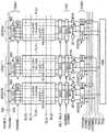
图7是示出实施方式一的液晶显示装置1的构成的框图。在图7中,详细地示出图5示出的模块500中的公共电极、第一电路CGW1、第二电路CGW2及驱动器用半导体装置DDIC。虽然是示意性示出,但图7配合实际的配置而描绘。FIG. 7 is a block diagram showing the configuration of the liquid
在同一图中,TL(0)~TL(p)是公共电极,在图7中,以公共电极TL(0)、TL(1)及TL(p)作为代表示出。另外,在图7中,在公共电极TL(0)、TL(1)及TL(p)上所描绘的虚线显示信号线,点划线显示扫描线GL(0)~GL(p)。In the same figure, TL(0) to TL(p) are common electrodes, and in FIG. 7 , the common electrodes TL(0), TL(1), and TL(p) are shown as representatives. In addition, in FIG. 7 , the dotted lines drawn on the common electrodes TL(0), TL(1), and TL(p) represent signal lines, and the dashed-dotted lines represent scanning lines GL(0) to GL(p).
在图7中,SP11~SP16显示形成各TFT基板300的端子,由端子 SP11~SP16构成对应一个公共电极的端子群(SP11~SP16)。由于在图7 中示出三个公共电极TL(0)、TL(1)及TL(p),因此,示出三组端子群(SP11~SP16)。端子SP11~SP16与驱动器用半导体装置DDIC的○印显示的端子连接,在显示期间,由驱动器用半导体装置DDIC的端子(○印)供给图像信号。另外,驱动器用半导体装置DDIC在触摸检测期间,使○印的端子为高阻抗状态。In FIG. 7 , SP11 to SP16 show terminals forming each of the
信号线选择器6(图1)由多个单位信号线选择器6(0)~6(p)构成。单位信号线选择器6(0)~6(p)分别具有彼此相同的构成,各个单位信号线选择器根据选择信号SEL1、SEL2的电压,将端子SP11~SP16 与对应该端子SP11~SP16的公共电极上配置的信号线连接。在图7中,以描绘在最左侧的单位信号线选择器6(0)为例说明,单位信号线选择器 6(0)根据选择信号SEL1、SEL2的电压,将端子SP11与信号线SL(0) 0(R)或SL(0)0(B)连接。例如,如果选择信号SEL1或者SEL2的电压为高电平,端子SP11连接信号线SL(0)0(R)或SL(0)0(B)。The signal line selector 6 ( FIG. 1 ) includes a plurality of unit signal line selectors 6( 0 ) to 6(p). The unit signal line selectors 6( 0 ) to 6(p) have the same configuration, respectively, and each unit signal line selector selects the terminals SP11 to SP16 and the corresponding terminals SP11 to SP16 in common according to the voltages of the selection signals SEL1 and SEL2 Connect to the signal line configured on the electrode. In FIG. 7 , the unit signal line selector 6( 0 ) depicted on the far left is taken as an example, and the unit signal line selector 6( 0 ) connects the terminal SP11 to the signal line SL according to the voltages of the selection signals SEL1 and SEL2 (0) 0(R) or SL(0)0(B) connection. For example, if the voltage of the selection signal SEL1 or SEL2 is at a high level, the terminal SP11 is connected to the signal line SL(0)0(R) or SL(0)0(B).
由此,在显示期间,通过选择性地使选择信号SEL1及SEL2为高电平,能够将从驱动器用半导体装置DDIC供给到端子SP11的图像信号供给到信号线SL(0)0(R)或SL(0)0(B)。剩余的端子SP12~SP16 也同样。在显示期间,驱动器用半导体装置DDIC向端子SP11~SP16的各个分时性供给图像信号,通过使选择信号SEL1、SEL2的电压高电平,能够适当地向信号线供给图像信号。Accordingly, in the display period, by selectively setting the selection signals SEL1 and SEL2 to high level, the image signal supplied from the driver semiconductor device DDIC to the terminal SP11 can be supplied to the signal line SL(0)0(R) or the signal line SL(0)0(R) SL(0)0(B). The same applies to the remaining terminals SP12 to SP16. During the display period, the driver semiconductor device DDIC supplies an image signal to each of the terminals SP11 to SP16 in a time-divisional manner, and by making the voltages of the selection signals SEL1 and SEL2 high, the image signal can be appropriately supplied to the signal lines.
另一方面,在触摸检测期间,驱动器用半导体装置DDIC使选择信号 SEL1、SEL2分别为高电平。由此,单位信号线选择器6(0)将端子SP11 连接信号线SL(0)0(R)及SL(0)0(B)。单位信号线选择器6(0) 将剩余的端子SP12~SP16的各个也同样地,各两个信号线连接一个端子。On the other hand, in the touch detection period, the driver semiconductor device DDIC sets the selection signals SEL1 and SEL2 to high level, respectively. Thereby, the unit signal line selector 6(0) connects the terminal SP11 to the signal lines SL(0)0(R) and SL(0)0(B). The unit signal line selector 6 ( 0 ) also connects each of the remaining terminals SP12 to SP16 to one terminal each of two signal lines in the same manner.
以单位信号线选择器6(0)为例进行说明,剩余的单位信号线选择器 6(1)~6(p)也相同。The unit signal line selector 6(0) will be described as an example, and the same applies to the remaining unit signal line selectors 6(1) to 6(p).
在该实施方式二中,第二电路CGW2由多个单位选择电路UCG2 (0)~UCG2(p)构成,第一电路(第一驱动电极电路)CGW1由多个单位驱动电极电路UCG1(0)~UCG1(p)构成。多个单位选择电路UCG2 (0)~UCG2(p)分别具有彼此相同的构成,多个单位驱动电极电路UCG(0)~UCG1(p)分别也具有相同的构成。单位选择电路UCG2(0)~ UCG2(p)及单位驱动电极电路UCG1(0)~UCG1(p)分别一对一对应公共电极TL(0)~TL(p)。若以图7显示的单位选择电路UCG2(0)、 UCG2(1)及UCG2(p),单位驱动电极电路UCG1(0)、UCG1(1)及 UCG1(p)为例进行说明,单位选择电路UCG2(0)和单位驱动电极电路UCG1(0)对应公共电极TL(0)。同样地,单位选择电路UCG2(1) 和单位驱动电极电路UCG1(1)对应公共电极TL(1),单位选择电路UCG2(p)和单位驱动电极电路UCG1(p)对应公共电极TL(p)。In the second embodiment, the second circuit CGW2 is composed of a plurality of unit selection circuits UCG2(0) to UCG2(p), and the first circuit (first drive electrode circuit) CGW1 is composed of a plurality of unit drive electrode circuits UCG1(0) ~UCG1(p) composition. Each of the plurality of unit selection circuits UCG2 ( 0 ) to UCG2 (p) has the same configuration as each other, and each of the plurality of unit drive electrode circuits UCG( 0 ) to UCG1 (p) also has the same configuration. The unit selection circuits UCG2(0)-UCG2(p) and the unit driving electrode circuits UCG1(0)-UCG1(p) correspond to the common electrodes TL(0)-TL(p) one-to-one, respectively. Taking the unit selection circuits UCG2(0), UCG2(1) and UCG2(p) and the unit driving electrode circuits UCG1(0), UCG1(1) and UCG1(p) shown in FIG. 7 as examples, the unit selection circuit UCG2(0) and the unit drive electrode circuit UCG1(0) correspond to the common electrode TL(0). Similarly, the unit selection circuit UCG2(1) and the unit drive electrode circuit UCG1(1) correspond to the common electrode TL(1), and the unit selection circuit UCG2(p) and the unit drive electrode circuit UCG1(p) correspond to the common electrode TL(p) .
接着,以单位选择电路UCG2(0)和与此对应的单位驱动电极电路 UCG1(0)为例,说明与对应的公共电极TL(0)的关系。单位选择电路 UCG2(0)具备开关电路SW2。向开关电路SW2供给与控制信号 VCOMSEL、xVCOMSEL及公共电极TL(0)对应的选择信号TP(0)。通过控制信号VCOMSEL、xVCOMSEL,开关电路SW2在触摸检测期间成为导通状态(接通(ON)状态),向端子SP16传递选择信号TP(0)。由此,选择信号TP(0)传递到控制线SS(0)。在该实施方式一中,控制线SS(0)为信号线SL(0)2(B),在显示期间,显示青(B)的图像信号从驱动器用半导体装置DDIC经由单位信号线选择器6(0)供给。此外,在图7中,由于信号线SL(0)2(B)显示与控制线SS(0)分时使用,因此,作为SS(0)[SL(0)2(B)]显示。Next, the relationship with the corresponding common electrode TL(0) will be described by taking the unit selection circuit UCG2(0) and the corresponding unit drive electrode circuit UCG1(0) as examples. The unit selection circuit UCG2(0) includes a switch circuit SW2. A selection signal TP(0) corresponding to the control signals VCOMSEL, xVCOMSEL and the common electrode TL(0) is supplied to the switch circuit SW2. By the control signals VCOMSEL and xVCOMSEL, the switch circuit SW2 is brought into the conductive state (ON state) during the touch detection period, and the selection signal TP( 0 ) is transmitted to the terminal SP16 . Thereby, the selection signal TP(0) is transmitted to the control line SS(0). In the first embodiment, the control line SS( 0 ) is the signal line SL( 0 ) 2 (B), and during the display period, the image signal for displaying cyan (B) is transmitted from the driver semiconductor device DDIC via the unit signal line selector 6 (0) Supply. In addition, in FIG. 7 , since the signal line SL(0)2(B) is displayed in a time-sharing manner with the control line SS(0), it is displayed as SS(0) [SL(0)2(B)].
与公共电极TL(0)对应的单位驱动电极电路UCG1(0)具有开关电路SW1和单位驱动电极驱动器12(0)。开关电路SW1连接在控制线SS(0)和单位驱动电极驱动器12(0)之间,通过控制信号VCOMSEL 控制。该开关电路SW1,在触摸检测期间,与控制线SS(0)和单位驱动电极驱动器12(0)电连接,在显示期间,与控制线SS(0)[SL(0)2 (B)]电性分离。换言之,开关电路SW1在显示期间是与控制线SS(0) [SL(0)2(B)]和单位驱动电极驱动器12(0)电性分离的分离电路。The unit drive electrode circuit UCG1(0) corresponding to the common electrode TL(0) has a switch circuit SW1 and a unit drive electrode driver 12(0). The switch circuit SW1 is connected between the control line SS(0) and the unit drive electrode driver 12(0), and is controlled by the control signal VCOMSEL. The switch circuit SW1 is electrically connected to the control line SS(0) and the unit drive electrode driver 12(0) during the touch detection period, and is electrically connected to the control line SS(0) [SL(0)2(B)] during the display period Electrical separation. In other words, the switch circuit SW1 is a separate circuit electrically separated from the control line SS(0) [SL(0)2(B)] and the unit drive electrode driver 12(0) during the display period.
在该实施方式一中,在显示期间,来自驱动器用半导体装置DDIC的图像信号向端子SP11~SP16供给,经由单位信号线选择器6(0)供给到信号线SL(0)。在图7的例子中,供给到信号线SL(0)0(R)、SL(0) 0(B)、SL(0)2(R)、SL(2)2(B),并按照图像信号进行图像的显示。In the first embodiment, in the display period, the image signal from the driver semiconductor device DDIC is supplied to the terminals SP11 to SP16 and supplied to the signal line SL( 0 ) via the unit signal line selector 6( 0 ). In the example of FIG. 7, it is supplied to the signal lines SL(0)0(R), SL(0)0(B), SL(0)2(R), SL(2)2(B), and the signal for image display.
另一方面,在触摸检测期间,驱动器用半导体装置DDIC使该输出端子(○印)进入高阻抗状态。此时,通过控制信号VCOMSEL、xVCOMSEL,构成单位选择电路UCG2(0)的开关电路SW2成为导通状态,由触摸用半导体装置7输出的选择信号TP(0)经由开关电路SW2传递到控制线 SS(0)[SL(0)2(B)],选择信号TP(0)经由该控制线SS(0)供给到单位驱动电极电路UCG1(0)。在单位驱动电极电路UCG1(0)中,在触摸检测期间,开关电路SW1通过控制信号VCOMSEL成为导通状态,将所供给的选择信号TP(0)供给到单位驱动电极驱动器12(0)。单位驱动电极驱动器12(0)根据所供给的选择信号TP(0)是否将公共电极指定为选择公共电极,将驱动电极TL(0)连接到信号布线503或电压布线 700。此处,向信号布线503供给作为公共驱动信号的控制信号TSVCOM,向电压布线700供给相当于接地电压的电压VCOMDC。On the other hand, during the touch detection period, the driver semiconductor device DDIC brings the output terminal (○ mark) into a high-impedance state. At this time, the switch circuit SW2 constituting the unit selection circuit UCG2(0) is turned on by the control signals VCOMSEL and xVCOMSEL, and the selection signal TP(0) output from the
当选择信号TP(0)指定对应的公共电极TL(0)作为选择公共电极时,单位驱动电极驱动器12(0)将信号布线503与公共电极TL(0)连接。另一方面,当选择信号TP(0)指定对应的公共电极TL(0)作为非选择公共电极时,单位驱动电极驱动器12(0)将电压布线700与公共电极TL(0)连接。由此,在触摸检测期间,当公共电极TL(0)被指定为选择公共电极时,作为驱动信号Tx(0)供给电压周期性变化的控制信号 TSVCOM。其结果,能够对该公共电极TL(0)的附近是否被触摸进行检测。另一方面,在触摸检测期间,当公共电极TL(0)被指定为非选择公共电极时,向这个公共电极TL(0)供给作为接地电压的电压VCOMDC。When the selection signal TP(0) designates the corresponding common electrode TL(0) as the selection common electrode, the unit driving electrode driver 12(0) connects the
构成单位选择电路UCG2(0)的开关电路SW2在显示期间成为高阻抗状态。另外,在显示期间,开关电路SW1作为分离电路动作。由此,供给到端子SP16的图像信号能够传递到信号线SL(0)2(B),并能够向连接信号线SL(0)2(B)的像素供给图像信号。The switch circuit SW2 constituting the unit selection circuit UCG2(0) is in a high-impedance state during the display period. In addition, during the display period, the switch circuit SW1 operates as a separate circuit. Thereby, the image signal supplied to the terminal SP16 can be transmitted to the signal line SL(0)2(B), and the image signal can be supplied to the pixel connected to the signal line SL(0)2(B).
其他单位选择电路UCG2(1)~UCG2(p)及单位驱动电极电路UCG1 (1)~UCG(p)分别与上述单位选择电路UCG2(0)及单位驱动电极电路UCG1(0)同样地动作。此外,在图7所示的例子中,与公共电极 TL(1)对应的信号线中,信号线SL(1)2(B)在触摸检测期间被用作控制信号SS(1)。另外,与公共电极TL(p)对应的信号线中,信号线 SL(p)2(B)在触摸检测期间被用作控制信号SS(p)。The other unit selection circuits UCG2(1) to UCG2(p) and the unit drive electrode circuits UCG1(1) to UCG(p) operate in the same manner as the unit selection circuit UCG2(0) and the unit drive electrode circuit UCG1(0) described above, respectively. Further, in the example shown in FIG. 7 , among the signal lines corresponding to the common electrode TL(1), the signal lines SL(1) 2(B) are used as the control signal SS(1) during touch detection. In addition, among the signal lines corresponding to the common electrode TL(p), the signal line SL(p)2(B) is used as the control signal SS(p) during touch detection.
在实施方式一中,可视为由单位驱动电极驱动器12(0)~12(p)构成图1显示的驱动电极驱动器12。In the first embodiment, it can be considered that the
<单位选择电路及单位驱动电极电路的构成><Configuration of unit selection circuit and unit drive electrode circuit>
接下来,说明图7中显示的单位选择电路UCG2(0)~UCG2(p) 及单位驱动电极电路UCG1(0)~UCG1(p)的构成。在此,以单位选择电路UCG2(0)及单位驱动电极电路UCG1(0)为代表进行说明。Next, the configurations of the unit selection circuits UCG2(0) to UCG2(p) and the unit drive electrode circuits UCG1(0) to UCG1(p) shown in FIG. 7 will be described. Here, the unit selection circuit UCG2( 0 ) and the unit drive electrode circuit UCG1( 0 ) are representatively described.
图8是示出实施方式一的液晶显示装置1的主要构成的电路图。在同一图中,显示单位选择电路UCG2(0)及单位驱动电极电路UCG1(0) 的构成和公共电极TL(0)这两部分的像素。为了避免图面复杂,图8中仅示出端子SP11~SP16中的端子SP11~SP13、SP16。另外,信号线也仅示出多条信号线中的信号线SL(0)0(R)、SL(0)0(G)、SL(0)0 (B)及信号线SL(0)2(B)。在此,由于信号线SL(0)2(B)在触摸检测期间发挥作为控制线SS(0)的功能,因此,显示为SS(0)[SL (0)2(B)]。此外,在同一图中,R、G、B显示像素。8 is a circuit diagram showing the main configuration of the liquid
此外,在图8中,显示触摸检测期间的单位信号线选择器6(0)的状态。即,显示通过选择信号SEL1、SEL2,单位信号线选择器6(0)与端子SP11~SP13、SP16的各个及信号线SL(0)连接的状态。In addition, in FIG. 8, the state of the unit signal line selector 6(0) during the touch detection period is shown. That is, the state where the unit signal line selector 6( 0 ) is connected to each of the terminals SP11 to SP13 and SP16 and the signal line SL( 0 ) by the selection signals SEL1 and SEL2 is shown.
单位信号线选择器6(0)具有通过选择信号SEL1接通(ON)/断开 (OFF)控制的多个开关S11和通过选择信号SEL2接通/断开控制的多个开关S12。在显示期间,通过选择信号SEL1和SEL2互补地成为高电平,开关S11和开关S12互补地成为接通状态。由此,向端子SP11~SP16分别供给的图像信号被供给到适合的信号线。另一方面,在触摸检测期间,没有特别的限制,选择信号SEL1及SEL2的双方可均为高电平。由此,如图8所示,端子SP11~SP16与公共电极TL(0)对应的多条信号线连接。The unit signal line selector 6(0) has a plurality of switches S11 controlled on/off by a selection signal SEL1 and a plurality of switches S12 controlled on/off by a selection signal SEL2. During the display period, when the selection signals SEL1 and SEL2 are complementarily brought to the high level, the switch S11 and the switch S12 are complementarily brought into the ON state. Thereby, the image signals supplied to the terminals SP11 to SP16, respectively, are supplied to appropriate signal lines. On the other hand, during the touch detection period, there is no particular limitation, and both the selection signals SEL1 and SEL2 may be at a high level. Thereby, as shown in FIG. 8 , the terminals SP11 to SP16 are connected to a plurality of signal lines corresponding to the common electrode TL( 0 ).
构成单位选择电路UCG2(0)的开关SW2具有P沟道型MOSFET (以下称为P型MOSFET)TP1和N沟道型MOSFET(以下称为N型 MOSFET)TN1。P型MOSFETTP1的一端的电极(源极或漏极)经由节点n1与端子SP16连接,N型MOSFETTN1的一端的电极(漏极或源极) 也经由节点n1与端子SP16连接。P型MOSFETTP1的另一端的电极(漏极或源极)和N型MOSFETTN1的另一端的电极(源极或漏极)共同与节点n2连接,并向该节点n2供给来自触摸用半导体装置7的选择信号 TP(0)。向P型MOSFETTP1的栅极供给控制信号xVCOMSEL,向N型 MOSFETTN1的栅极供给控制信号VCOMFEL。The switch SW2 constituting the unit selection circuit UCG2(0) includes a P-channel MOSFET (hereinafter referred to as a P-type MOSFET) TP1 and an N-channel MOSFET (hereinafter referred to as an N-type MOSFET) TN1. One end electrode (source or drain) of P-type MOSFETTP1 is connected to terminal SP16 via node n1, and one end electrode (drain or source) of N-type MOSFETTN1 is also connected to terminal SP16 via node n1. The electrode (drain or source) at the other end of the P-type MOSFETTP1 and the electrode (source or drain) at the other end of the N-type MOSFETTN1 are connected to the node n2 in common, and the node n2 is supplied with the
在触摸检测期间,触摸用半导体装置7使控制信号VCOMSEL成为高电平,使控制信号xVCOMSEL成为低电平。另外,触摸用半导体装置7 使作为选择公共电极指定的公共电极对应的选择信号为高电平,使作为非选择公共电极指定的公共电极对应的指定信号为低电平。例如,将公共电极TL(0)指定为选择公共电极时,触摸用半导体装置7使公共电极TL (0)对应的选择信号TP(0)为高电平,将公共电极TL(0)作为非选择公共电极指定时,使选择信号TP(0)为低电平。During the touch detection period, the
由此,构成开关电路SW2的P型MOSFETTP1及N型MOSFETTN1 分别在触摸检测期间成为接通状态,向节点n2供给的选择信号TP(0) 经由节点n1供给到端子SP16。另一方面,在显示期间,控制信号 VCOMSEL成为低电平,控制信号xVCOMSEL成为高电平。由此,P型MOSFETTP1及N型MOSFETTN1分别成为断开状态。其结果,作为开关电路SW2的输出端子节点n1成为高阻抗状态。Thereby, the P-type MOSFETTP1 and the N-type MOSFETTN1 constituting the switch circuit SW2 are respectively turned on during the touch detection period, and the selection signal TP(0) supplied to the node n2 is supplied to the terminal SP16 via the node n1. On the other hand, during the display period, the control signal VCOMSEL becomes the low level, and the control signal xVCOMSEL becomes the high level. Thereby, the P-type MOSFETTP1 and the N-type MOSFETTN1 are respectively turned off. As a result, the node n1 which is the output terminal of the switch circuit SW2 is brought into a high-impedance state.
在触摸检测期间,向端子SP16供给的选择信号TP(0)传播控制线 SS(0),供给到单位驱动电极电路UCG1(0)。即,选择信号TP(0)供给到单位驱动电极电路UCG1(0)内的开关电路SW1。开关电路SW1具有连接在选择线SS(0)和信号布线800之间的开关S40。开关S40通过控制信号VCOMSEL进行开关控制。如前所述,由于控制信号VCOMSEL 在触摸检测期间成为高电平,因此,开关电路SW1在触摸检测期间成为接通状态,在显示期间成为断开状态。During the touch detection period, the selection signal TP(0) supplied to the terminal SP16 is propagated to the control line SS(0) and supplied to the unit drive electrode circuit UCG1(0). That is, the selection signal TP(0) is supplied to the switch circuit SW1 in the unit drive electrode circuit UCG1(0). The switch circuit SW1 has a switch S40 connected between the selection line SS( 0 ) and the
构成单位驱动电极电路UCG1(0)的单位驱动电极驱动器12(0)具有P型MOSFETTP2、缓冲电路BF1、换流电路IV1、开关S20~S23及开关S30~S33。开关S20~S23分别并列连接在电压布线700和公共电极 TL(0)之间,开关S30~S33分别并列连接在信号布线503和公共电极 TL(0)之间。开关S20~S23分别根据换流电路IV1的输出信号进行接通/断开控制,开关S30~S33分别根据缓冲电路BF1的输出信号进行接通 /断开控制。换流电路IV1的输入和缓冲电路BF1的输入连接信号布线800。另外,该信号布线800与P型MOSFETTP2的漏极连接。该P型 MOSFETTP2的源极与相当于接地电压的电压VGL连接,向其栅极供给控制信号VCOMSEL。The unit drive electrode driver 12 ( 0 ) constituting the unit drive electrode circuit UCG1 ( 0 ) includes a P-type MOSFET TP2 , a buffer circuit BF1 , a commutation circuit IV1 , switches S20 to S23 , and switches S30 to S33 . The switches S20 to S23 are connected in parallel between the
由于在触摸检测期间,控制信号VCOMSEL成为高电平,P型 MOSFETTP2成为断开状态。由此,信号布线800的电压成为与经由开关电路SW1所供给的选择信号TP(0)的电压相同的电压。将公共电极TL (0)指定为选择公共电极时,由于选择信号TP(0)成为高电平,缓冲电路BF1输出高电平,换流电路IV1输出低电平。由此,开关S30~S33 分别成为接通状态,公共电极TL(0)经由开关S30~S33连接信号布线 503。供给到信号布线503的控制信号TSVCOM是在触摸检测期间,其电压周期性变化的时钟信号。因此,将公共电极TL(0)指定为选择公共电极时,供给电压周期性变化的驱动信号,能够进行该公共电极TL(0)的附近是否被触摸的判定。During the touch detection period, the control signal VCOMSEL is at a high level, and the P-type MOSFETTP2 is turned off. Thereby, the voltage of the
与此相对,公共电极TL(0)被指定为非选择公共电极时,选择信号 TP(0)成为低电平。该选择信号TP(0)的低电平传递信号布线800并向缓冲电路BF1及换流电路IV1供给。由此,缓冲电路BF1输出低电平,换流电路IV1输出高电平。换流电路IV的输出为高电平,从而开关S20~ S23分别成为接通状态。另一方面,缓冲电路BF1的输出为低电平,从而开关S30~S33分别成为断开状态。其结果,公共电极TL(0)经由开关 S20~S23连接电压布线700,供给接地电压。作为非选择公共电极指定公共电极TL(0)时,由于公共电极TL(0)的电压被固定在接地电压,因此即使触摸该公共电极TL(0)的附近,也不能进行触摸的检测。On the other hand, when the common electrode TL(0) is designated as a non-selected common electrode, the selection signal TP(0) becomes a low level. The low level of the selection signal TP( 0 ) transmits the
在显示期间,由于控制信号VCOMSEL成为低电平,所以开关电路 SW1进入断开状态。其结果,信号布线800和信号线SL(0)2(B)电分离,从而能够防止图像信号向单位驱动电极驱动器12(0)的供给。另外,此时,由于P型MOSFETTP2为接通状态,因此,经由P型MOSFETTP2 向信号布线800供给电压VGL。其结果,缓冲电路BF1的输出为低电平,换流电路IV1的输出为高电平。换流电路IV1的输出为高电平,开关S20~ S23分别成为接通状态。由此,在显示期间,经由开关S20~S23,向公共电极TL(p)供给电压VCOMDC。此时,电压VCOMDC是与接地电压对应的电压VCOMDC。通过这样的方式,在显示期间,能够向公共电极 TL(0)的显示供给适当的电压VCOMDC。During the display period, since the control signal VCOMSEL becomes a low level, the switch circuit SW1 is turned off. As a result, the
<单位选择电路及单位驱动电极电路的动作><Operation of the unit selection circuit and the unit drive electrode circuit>
接着,说明图8显示的液晶显示装置1的动作。图9的(A)~(E) 是示出图8显示的液晶显示装置1的动作的波形图。在图9中,横轴表示时间,纵轴表示电压。图9的(A)显示选择信号SEL1的波形,图9的 (B)显示控制信号VCOMSEL的波形,图9的(C)显示控制信号TSVCOM的波形。Next, the operation of the liquid
在图9中,显示触摸检测期间和显示期间的波形,关于触摸检测期间示出了图8显示的公共电极TL(0)相关的波形。即,图9的(D)显示选择信号TP(0)的波形,图9的(E)显示供给到公共电极TL(0)的驱动信号Tx(0)的波形。在图9中,“触摸检测期间(选择公共电极)”显示由触摸用半导体装置7指定公共电极TL(0)为选择公共电极的情况。另外,“触摸检测期间(非选择公共电极)”显示由触摸用半导体装置7指定公共电极TL(0)为非选择公共电极的情况。In FIG. 9 , the waveforms during the touch detection period and the display period are shown, and the waveform related to the common electrode TL( 0 ) shown in FIG. 8 is shown for the touch detection period. That is, FIG. 9(D) shows the waveform of the selection signal TP( 0 ), and FIG. 9(E) shows the waveform of the drive signal Tx( 0 ) supplied to the common electrode TL( 0 ). In FIG. 9 , “touch detection period (selection of common electrode)” shows the case where the common electrode TL( 0 ) is designated as the selection common electrode by the
如图9所示,触摸检测期间和显示期间交替产生还是从触摸检测期间转向显示期间之前,没有特别的限定,但设置信号线预充期间。在该信号线预充期间,预充电信号线SL(0)~SL(p),使各信号线的电压为规定的电压。由此,当显示期间转移时,能够抑制不希望的显示发生。As shown in FIG. 9 , whether the touch detection period and the display period are alternately generated or before the touch detection period turns to the display period is not particularly limited, but a signal line precharge period is set. In this signal line precharge period, the signal lines SL( 0 ) to SL(p) are precharged so that the voltage of each signal line becomes a predetermined voltage. Thereby, when the display period is shifted, it is possible to suppress the occurrence of unintended display.
在显示期间,触摸用半导体装置7使控制信号VCOMSEL为低电平,使控制信号TSVCOM为低电平。另外,选择信号SEL1、SEL2互补地为高电平。在图9的(A)中,仅显示了选择信号SEL1的波形,但期待理解为选择信号SEL2在选择信号SEL1为低电平时成为高电平。由此,图 8显示的开关S11和S12交替进入接通状态,将向端子SP11~SP16供给的图像信号分时供给到适当的信号线。During the display period, the
另外,在显示期间,控制信号VCOMSEL成为低电平,图8显示的P 型MOSFETTP2为导通状态,开关电路SW1成为非导通状态。由此,信号布线800从信号线SL(0)2(B)分离,成为低电平的电压VGL。由于低电平的电压VGL被供给到换流电路IV1,开关S20~S23进入接通状态,相当于接地电压的电压VCOMDC作为显示时的驱动电压,经由开关 S20~S23被供给到公共电极TL(0)。In addition, during the display period, the control signal VCOMSEL is at a low level, the P-type MOSFET TP2 shown in FIG. 8 is turned on, and the switch circuit SW1 is turned off. Thereby, the
并且,由于控制信号xVCOMSEL是相对于控制信号VCOMSEL相位相反的信号,因此在显示期间,成为高电平。由此,构成图8显示的开关电路SW2的P型MOSFETTP1及N型MOSFETTN1的双方为断开状态,开关电路SW2的输出节点n1进入高阻抗状态。由此,从驱动器用半导体装置DDIC供给到端子SP11~SP16的图像信号传递到信号线SL(0)0 (R)、SL(0)0(G)、SL(0)0(B)~SL(0)2(R)、SL(0)2(G)、 SL(0)2(B),根据图像信号进行显示。In addition, since the control signal xVCOMSEL is a signal whose phase is opposite to that of the control signal VCOMSEL, it becomes a high level during the display period. Accordingly, both the P-type MOSFETTP1 and the N-type MOSFET TN1 constituting the switch circuit SW2 shown in FIG. 8 are turned off, and the output node n1 of the switch circuit SW2 is brought into a high-impedance state. As a result, the image signals supplied from the driver semiconductor device DDIC to the terminals SP11 to SP16 are transmitted to the signal lines SL(0)0(R), SL(0)0(G), and SL(0)0(B) to SL (0)2(R), SL(0)2(G), and SL(0)2(B) are displayed according to the image signal.
在触摸检测期间,驱动器用半导体装置DDIC使选择信号SEL1、SEL2 的双方为高电平。由此,图8显示的开关S11和S12双方成为接通状态。另外,触摸用半导体装置7使控制信号VCOMSEL为高电平,使控制信号 TSVCOM的电压周期性变化。During the touch detection period, the driver semiconductor device DDIC sets both the selection signals SEL1 and SEL2 to high level. As a result, both switches S11 and S12 shown in FIG. 8 are turned on. In addition, the
触摸检测期间是触摸检测期间(选择公共电极)时,触摸用半导体装置7使选择信号TP(0)为高电平。控制信号VCOMSEL为高电平,控制信号xVCOMSEL为低电平,因此开关电路SW2为导通状态,高电平的选择信号TP(0)经由开关电路SW2供给到端子SP16。此时,驱动器用半导体装置DDIC的输出端子(图7的○印)为高阻抗状态,供给到端子SP16 的选择信号TP(0)传播控制线SS(0),供给到单位驱动电极电路UCG1 (0)。When the touch detection period is the touch detection period (the common electrode is selected), the
在单位驱动电极电路UCG1(0)中,由于控制信号VCOMSEL为高电平状态,开关电路SW1为导通状态,P型MOSFETTP2为断开状态。因此,控制线SS(0)经由开关电路SW1连接信号布线800,信号布线 800的电压为高电平。信号布线800的电压为高电平,从而缓冲电路BF1的输出为高电平,换流电路IV1输出低电平。由此,开关S20~S23进入断开状态,开关S30~S33进入接通状态。开关S30~S33成为接通状态,公共电极TL(0)经由开关S30~S33连接信号布线503。由于其电压周期性变化,信号布线503的控制信号TSVCOM向驱动电极TL(0)供给如图9(E)所示电压周期性变化的驱动信号Tx(0)。由此,如在图2说明的那样,能够进行驱动电极TL(0)的附近是否被触摸的检测。In the unit drive electrode circuit UCG1( 0 ), since the control signal VCOMSEL is in the high-level state, the switch circuit SW1 is in the ON state, and the P-type MOSFETTP2 is in the OFF state. Therefore, the control line SS(0) is connected to the
另一方面,触摸检测期间是触摸检测期间(非选择公共电极)时,触摸用半导体装置7使选择信号TP(0)为低电平。控制信号VCOMSEL为高电平,控制信号xVCOMSEL为低电平,因此开关电路SW2为导通状态,低电平的选择信号TP(0)经由开关电路SW2供给到端子SP16。此时,驱动器用半导体装置DDIC的输出端子(图7的○印)为高阻抗状态,供给到端子SP16的选择信号TP(0)传播控制线SS(0),供给到单位驱动电极电路UCG1(0)。On the other hand, when the touch detection period is the touch detection period (the common electrode is not selected), the
在单位驱动电极电路UCG1中,由于控制信号VCOMSEL为高电平状态,开关电路SW1为导通状态,P型MOSFETTP2为断开状态。因此,控制线SS(0)经由开关电路SW1连接信号布线800,信号布线800的电压为低电平。信号布线800的电压为低电平,从而缓冲电路BF1的输出为低电平,换流电路IV1的输出为高电平。由此,开关S30~S33进入断开状态,开关S20~S23进入接通状态。开关S20~S23成为接通状态,公共电极TL(0)经由开关S20~S23连接电压布线700。其结果,不向公共电极TL(0)供给其电压周期性变化的控制信号TSVCOM,而供给作为接地电压的电压VCOMDC。由此,即便公共电极TL(0)的附近被触摸,检测信号的电压不发生变化,不进行触摸有无的检测。In the unit drive electrode circuit UCG1, since the control signal VCOMSEL is in the high-level state, the switch circuit SW1 is in the ON state, and the P-type MOSFET TP2 is in the OFF state. Therefore, the control line SS( 0 ) is connected to the
以公共电极TL(0)、单位选择电路UCG2(0)及单位驱动电极电路 UCG1(0)为代表例进行了说明,公共电极TL(1)~TL(p)、单位选择电路UCG2(1)~UCG2(p)及单位驱动电极电路UCG1(1)~UCG1 (p)的构成及动作也相同。The common electrode TL(0), the unit selection circuit UCG2(0), and the unit drive electrode circuit UCG1(0) are used as representative examples for description. The common electrodes TL(1) to TL(p), the unit selection circuit UCG2(1) The configurations and operations of to UCG2(p) and the unit drive electrode circuits UCG1(1) to UCG1(p) are also the same.
在实施方式一中,由于能够以少数元件(P型MOSFETTP1、N型 MOSFETTN1)构成沿着液晶面板2的短边2-D配置的第二电路CGW2,从而可以窄化液晶面板2的下侧边框。另外,由于沿着液晶面板2的短边 2-U配置的第一电路(第一驱动电极电路)CGW1驱动公共电极TL(0)~ TL(p),能够进行的触摸的检测。此外,作为从第二电路CGW2向第一电路CGW1传递选择信号的布线,在触摸检测期间,通过将显示时传递图像信号的信号线用作控制线,能够抑制显示面板2的侧面边框的变大。In the first embodiment, since the second circuit CGW2 arranged along the short side 2-D of the
在图7及图8中,作为控制线SS(0),使用信号线SL(0)2(B) 的例子进行了说明,但不限定于此。公共电极TL(0)对应的信号线SL (0)的多条信号线,例如所有的信号线SL(0)0(R)、SL(0)0(G)、 SL(0)0(B)~SL(0)2(R)、SL(0)2(G)、SL(0)2(B)或这些信号线的至少一部分信号线可用作控制线SS(0)。此时,例如,也可在端子SP11~SP16分别设置相当于开关电路SW2的开关电路,将开关电路的输出节点n1与端子SP11~SP16连接,在各个信号线和信号布线800 之间设置相当于开关电路SW1的开关电路。信号线SL(1)~SL(p)分别也能够和信号线SL(0)同样地,不是一条信号线而是至少一部分的信号线被兼用作控制线。In FIGS. 7 and 8 , an example in which the signal line SL( 0 ) 2 (B) is used as the control line SS( 0 ) has been described, but the present invention is not limited to this. Multiple signal lines of the signal line SL(0) corresponding to the common electrode TL(0), for example, all the signal lines SL(0)0(R), SL(0)0(G), SL(0)0(B ) to SL(0)2(R), SL(0)2(G), SL(0)2(B) or at least a part of these signal lines may be used as the control line SS(0). In this case, for example, a switch circuit corresponding to the switch circuit SW2 may be provided at the terminals SP11 to SP16 , the output node n1 of the switch circuit may be connected to the terminals SP11 to SP16 , and a switch circuit corresponding to the
这样,在公共电极对应的各个信号线SL(0)~SL(p)中,通过将多条信号线兼用作控制线,能够减少选择信号TP(0)~TP(p)传播时的延迟时间。In this way, in each of the signal lines SL( 0 ) to SL(p) corresponding to the common electrodes, by using a plurality of signal lines also as control lines, it is possible to reduce the delay time when the selection signals TP( 0 ) to TP(p) propagate. .
(实施方式二)(Embodiment 2)
<液晶显示装置1的结构><Configuration of Liquid
图10是示出实施方式二涉及的液晶显示装置1的构成的框图。在图 10中,将图5示出的模块500中的公共电极、第一电路CGW1、第二电路CGW2及驱动器用半导体装置DDIC详细地示出。虽然是示意性示出,但图10配合实际的配置而描绘。10 is a block diagram showing the configuration of the liquid
图10显示的液晶显示装置的结构与图7显示的液晶显示装置的构成类似。在此,以和图7显示的液晶显示装置的不同点为主进行说明。首先,说明不同点的概要,在实施方式二涉及的液晶显示装置1中,第一电路 CGW1包括与实施方式一相同的第一驱动电极电路,第二电路CGW2也包括向公共电极TL(0)~TL(p)供给驱动信号Tx(0)~Tx(p)的第二驱动电极电路。另外,该实施方式二涉及的液晶显示装置1包括将公共电极TL(0)~TL(p)在显示期间与电压VCOMDC连接,在触摸检测期间与端子SP11~SP16中的一部分端子连接的切换电路100。The structure of the liquid crystal display device shown in FIG. 10 is similar to that of the liquid crystal display device shown in FIG. 7 . Here, the description will be given mainly on the differences from the liquid crystal display device shown in FIG. 7 . First, the outline of the difference will be described. In the liquid
第一电路CGW1和实施方式一同样地为第一驱动电极电路,其包括多个第一单位驱动电极电路UCG1(0)~UCG1(p)。该第一单位驱动电极电路UCG1(0)~UCG1(p)与公共电极TL(0)~TL(p)一对一对应,彼此具有相同的构成。以第一单位驱动电极电路UCG1(0)为代表进行说明,第一单位驱动电极电路UCG1(0)包括第一单位驱动电极驱动器12-1(0)和开关电路SW3。第一单位驱动电极驱动器12-1(0)具有与实施方式一叙述的单位驱动电极驱动器12(0)相同的构成。The first circuit CGW1 is a first drive electrode circuit like the first embodiment, and includes a plurality of first unit drive electrode circuits UCG1( 0 ) to UCG1(p). The first unit drive electrode circuits UCG1(0) to UCG1(p) correspond one-to-one with the common electrodes TL(0) to TL(p), and have the same configuration. The first unit drive electrode circuit UCG1( 0 ) will be described as a representative. The first unit drive electrode circuit UCG1( 0 ) includes a first unit drive electrode driver 12 - 1 ( 0 ) and a switch circuit SW3 . The first unit drive electrode driver 12-1(0) has the same configuration as the unit drive electrode driver 12(0) described in the first embodiment.
开关电路SW3由控制信号VCOMSEL控制,在触摸检测期间,将经由控制线SS(0)供给的选择信号传递到信号布线800。另外,在触摸检测期间,开关电路SW3将除去与控制线SS(0)对应的信号线的信号线与公共电极TL(0)连接。The switch circuit SW3 is controlled by the control signal VCOMSEL, and transmits the selection signal supplied via the control line SS( 0 ) to the
第二电路CGW2是第二驱动电极电路,其包括多个第二单位驱动电极电路UCG2(0)~UCG2(p)。该第二单位驱动电极电路UCG2(0)~ UCG2(p)与公共电极TL(0)~TL(p)一对一对应,彼此具有相同的构成。以第二单位驱动电极电路UCG2(0)为代表进行说明,则第二单位驱动电极电路UCG2(0)包括第二单位驱动电极驱动器12-2(0)和开关电路SW2。第二单位驱动电极驱动器12-2(0)和第一单位驱动电极驱动器12-1(0)类似,在触摸检测期间,当选择信号TP(0)将公共电极 TL(0)指定为选择公共电极时,将电压周期性变化的控制信号TSVCOM 向端子SP11~SP16中的规定的端子SP11~SP15供给。The second circuit CGW2 is a second drive electrode circuit, which includes a plurality of second unit drive electrode circuits UCG2( 0 ) to UCG2(p). The second unit drive electrode circuits UCG2(0) to UCG2(p) correspond to the common electrodes TL(0) to TL(p) one-to-one, and have the same configuration. Taking the second unit drive electrode circuit UCG2(0) as a representative for description, the second unit drive electrode circuit UCG2(0) includes a second unit drive electrode driver 12-2(0) and a switch circuit SW2. The second unit driving electrode driver 12-2(0) is similar to the first unit driving electrode driver 12-1(0), during touch detection, when the selection signal TP(0) designates the common electrode TL(0) as the selection common During the electrode operation, a control signal TSVCOM whose voltage is periodically changed is supplied to predetermined terminals SP11 to SP15 among the terminals SP11 to SP16.
开关电路SW2具有与实施方式一中叙述的开关电路SW2相同的构成,在触摸检测期间,向控制线SS(0)供给选择信号TP(0)。The switch circuit SW2 has the same configuration as the switch circuit SW2 described in the first embodiment, and supplies the selection signal TP( 0 ) to the control line SS( 0 ) during the touch detection period.
切换电路100也由多个单位切换电路100(0)~100(p)构成。单位切换电路100(0)~100(p)与公共电极TL(0)~TL(p)一对一对应,彼此具有相同的构成。以单位切换电路100(0)为代表进行说明,单位切换电路100(0)对应公共电极TL(0),按照控制信号VCOMSEL,将对应的公共电极TL(0)与规定的端子SP11~SP15或电压VCOMDC连接。即,控制信号VCOMSEL在显示显示期间时,单位切换电路100(0)将对应的公共电极TL(0)与电压VCOMDC连接,控制信号VCOMSEL在显示触摸检测期间时,将公共电极TL(0)连接到端子SP11~SP15。The
在触摸检测期间,通过单位切换电路100(0),公共电极TL(0)与端子SP11~SP15连接,来自第二单位驱动电极驱动器12-2(0)的驱动信号经由端子SP11~SP15供给到公共电极TL(0)。此时,也向与控制线 SS(0)对应的除信号线SL(0)2(B)之外的信号线供给来自第二单位驱动电极驱动器12-2(0)的驱动信号。During the touch detection period, the common electrode TL(0) is connected to the terminals SP11 to SP15 through the unit switching circuit 100(0), and the driving signal from the second unit driving electrode driver 12-2(0) is supplied to the terminals SP11 to SP15 through the terminals SP11 to SP15. The common electrode TL(0). At this time, the drive signal from the second unit drive electrode driver 12-2(0) is also supplied to the signal lines other than the signal line SL(0)2(B) corresponding to the control line SS(0).
在触摸检测期间,与实施方式一同样地,经由开关SW2,向控制线 SS(0)[SL(0)2(B)]供给选择信号TP(0)。该选择信号TP(0)传递控制线SS(0)[SL(0)2(B)],经由开关电路SW3供给到信号布线 800。与实施方式一的驱动电极驱动器12(0)同样地,第一单位驱动电极驱动器12-1(0)按照信号布线800的电压,形成驱动信号,并向公共电极TL(0)供给。此时,开关电路SW3将除去与控制线SS(0)对应的信号线SL(0)2(B)的信号线与公共电极TL(0)连接。因此,由第一单位驱动电极驱动器12-1(0)所形成的驱动信号也被供给到除与控制线SS(0)对应的信号线[SL(0)2(B)]之外的信号线。During the touch detection period, as in the first embodiment, the selection signal TP(0) is supplied to the control line SS(0) [SL(0)2(B)] via the switch SW2. The selection signal TP(0) is transmitted to the control line SS(0) [SL(0)2(B)], and is supplied to the
由此,在触摸检测期间,通过沿着液晶面板2的各个短边2-U(第一边)、2-D(第二边)配置的第一单位驱动电极驱动器12-1(0)及第二单位驱动电极驱动器12-2(0),从公共电极TL(0)的两侧供给驱动信号。另外,通过开关电路SW3及切换电路100(0),除控制线SS(0)[SL(0) 2(B)]之外的信号线与公共电极TL(0)并列连接,能够使合成阻抗降低。其结果,即使第一单位驱动电极驱动器12-1(0)及第二单位驱动电极驱动器12-2(0)的驱动能力降低,能够驱动公共电极TL(0),从而可实现第一及第二单位驱动电极驱动器12-1(0)、12-2(0)的小型化。由此,液晶面板2的上侧及下侧的边框能够变窄。Thus, during the touch detection period, the first unit drive electrode drivers 12 - 1 ( 0 ) and the The second unit drive electrode driver 12-2(0) supplies drive signals from both sides of the common electrode TL(0). In addition, by the switch circuit SW3 and the switch circuit 100(0), the signal lines other than the control line SS(0) [SL(0) 2(B)] are connected in parallel with the common electrode TL(0), so that the combined impedance can be made reduce. As a result, even if the driving capabilities of the first unit driving electrode driver 12-1(0) and the second unit driving electrode driver 12-2(0) are lowered, the common electrode TL(0) can be driven, and the first and second unit driving electrode drivers 12-2(0) can be driven. Miniaturization of the two-unit drive electrode drivers 12-1(0) and 12-2(0). As a result, the upper and lower frames of the
另外,与实施方式一同样地,将在显示期间作为信号线SL(0)2(B) 发挥功能的布线用作传递选择信号TP(0)的控制线,因此,能够防止液晶面板2的右侧及左侧的边框的变大。Also, as in the first embodiment, the wiring that functions as the signal line SL( 0 ) 2 (B) during the display period is used as the control line for transmitting the selection signal TP( 0 ). The side and left borders are enlarged.
以第一单位驱动电极电路UCG1(0)、第二单位驱动电极电路UCG2 (0)及单位切换电路100(0)作为代表进行了说明,但剩余的第一单位驱动电极电路UCG1(1)~UCG1(p)、第二单位驱动电极电路UCG2(1)~ UCG2(p)及单位切换电路100(1)~100(p)的构成及动作相同。The first unit drive electrode circuit UCG1 ( 0 ), the second unit drive electrode circuit UCG2 ( 0 ), and the unit switching circuit 100 ( 0 ) have been described as representatives, but the remaining first unit drive electrode circuits UCG1 ( 1 ) to UCG1(p), the second unit drive electrode circuits UCG2(1) to UCG2(p), and the unit switching circuits 100(1) to 100(p) have the same configurations and operations.
<第一单位驱动电极电路及第二单位驱动电极电路的构成><Configuration of the first unit drive electrode circuit and the second unit drive electrode circuit>
接下来,说明图10中显示的第一单位驱动电路UCG1(0)~UCG1 (p)及第二单位驱动电极电路UCG2(0)~UCG2(p)的构成。在此,以第一单位驱动电路UCG1(0)及第二单位驱动电极电路UCG2(0)为代表,使用图11进行说明。Next, the configurations of the first unit drive circuits UCG1(0) to UCG1(p) and the second unit drive electrode circuits UCG2(0) to UCG2(p) shown in FIG. 10 will be described. Here, the first unit drive circuit UCG1( 0 ) and the second unit drive electrode circuit UCG2( 0 ) will be described with reference to FIG. 11 .
图11是示出实施方式二涉及的液晶显示装置1的主要构成的电路图。由于图11显示的电路图和图8显示的电路图类似,因此,在此主要说明不同点。11 is a circuit diagram showing the main configuration of the liquid
包括在第一单位驱动电极电路UCG1(0)的第一单位驱动电极驱动器12-1(0)的构成和图8显示的单位驱动电极驱动器12(0)的构成相同。即,第一单位驱动电极驱动器12-1(0)具有P型MOSFETTP2、开关S20~S23、S30~S33、阻抗电路IV1及缓冲电路BF1。The configuration of the first unit driving electrode driver 12-1(0) included in the first unit driving electrode circuit UCG1(0) is the same as that of the unit driving electrode driver 12(0) shown in FIG. 8 . That is, the first unit drive electrode driver 12-1(0) includes a P-type MOSFET TP2, switches S20 to S23, S30 to S33, an impedance circuit IV1, and a buffer circuit BF1.
开关电路SW3具备通过控制信号VCOMSEL进行开关控制的开关 S40~S43。在此,与图8同样,开关S40连接在信号布线800和信号线 SL(0)2(B)之间。与实施方式一相同,该信号线SL(0)2(B)在显示期间被用于传递图像信号,在触摸检测期间,被用作传递选择信号的控制线SS(0)。在显示期间,由于开关S40通过控制信号VCOMSEL进入断开状态,因此作为分离信号布线800和信号线SL(0)2(B)的分离电路发挥功能。The switch circuit SW3 includes switches S40 to S43 whose switching is controlled by the control signal VCOMSEL. Here, the switch S40 is connected between the
开关S41~S43连接在除公共电极TL(0)和信号线SL(0)2(B) 之外的信号线之间。在图10中,示出连接在公共电极TL(0)和信号线 SL(0)0(R)、SL(0)0(G)、SL(0)0(B)之间的开关S41~S43。当控制信号VCOMSEL显示触摸检测期间时,即控制信号VCOMSEL为高电平时,开关S41~S43分别成为接通状态。另一方面,当控制信号 VCOMSEL显示显示期间时,即控制信号VCOMSEL为低电平时,开关 S41~S43分别成为断开状态。The switches S41 to S43 are connected between the signal lines other than the common electrode TL(0) and the signal line SL(0)2(B). In FIG. 10 , switches S41 to SL(0)0(B) connected between the common electrode TL(0) and the signal lines SL(0)0(R), SL(0)0(G), and SL(0)0(B) are shown. S43. When the control signal VCOMSEL shows a touch detection period, that is, when the control signal VCOMSEL is at a high level, the switches S41 to S43 are turned on, respectively. On the other hand, when the control signal VCOMSEL shows a display period, that is, when the control signal VCOMSEL is at a low level, the switches S41 to S43 are turned off, respectively.
与实施方式一同样地,在触摸检测期间,经由控制线SS(0)及开关 S40,选择信号被供给到信号布线800。选择信号将公共电极TL(0)指定为选择公共电极时,选择信号TP(0)成为高电平。由此,与图8说明的同样,第一单位驱动电极驱动器12-1(0)内的开关S30~S33分别成为接通状态,控制信号TSVCOM作为驱动信号Tx(0)被供给到公共电极TL (0)。此时,由于开关电路SW3内的开关S41~S43也成为接通状态,因此,经由信号线SL(0)0(R)、SL(0)0(G)、SL(0)0(B)分别经由开关S41~S43,将控制信号TSVCOM作为驱动信号Tx(0)供给。As in the first embodiment, during the touch detection period, the selection signal is supplied to the
此处,应注意在被用作控制线SS(0)的信号线SL(0)2(B)和公共电极TL(0)之间未设置开关。在触摸检测期间,由于该信号线SL(0) 2(B)作为用于传递选择信号的控制线SS(0)使用,为了不供给驱动信号而未设置开关。Here, it should be noted that no switch is provided between the signal line SL(0)2(B) used as the control line SS(0) and the common electrode TL(0). During touch detection, since the signal lines SL(0) to 2(B) are used as control lines SS(0) for transmitting selection signals, switches are not provided so as not to supply drive signals.
另外,在触摸检测期间,选择信号将公共电极TL(0)指定为非选择公共电极时,选择信号成为低电平。由此,与图8说明的同样,第一单位驱动电极驱动器12-1(0)内的开关S20~S23分别成为接通状态。由此,向公共电极TL(0)及信号线SL(0)0(R)、SL(0)0(G)、SL(0)0 (B)供给接地电压对应的电压VCOMDC。In addition, during the touch detection period, when the selection signal designates the common electrode TL(0) as a non-selected common electrode, the selection signal becomes a low level. As a result, the switches S20 to S23 in the first unit drive electrode driver 12 - 1 ( 0 ) are turned on, respectively, as described in FIG. 8 . Thereby, the voltage VCOMDC corresponding to the ground voltage is supplied to the common electrode TL(0) and the signal lines SL(0)0(R), SL(0)0(G), and SL(0)0(B).
在显示期间,由于控制信号VCOMSEL成为低电平,开关电路SW3 内的开关S40~S43成为断开状态。由此,信号线SL(0)2(B)从信号布线800分离,与图8所述相同,开关S20~S23成为接通状态,向公共电极TL(0)供给来自第一单位驱动电极电路UCG1(0)的显示时的驱动电压。During the display period, since the control signal VCOMSEL becomes the low level, the switches S40 to S43 in the switch circuit SW3 are turned off. As a result, the signal line SL( 0 ) 2 (B) is separated from the
第二单位驱动电极电路UCG2(0)具有第二单位驱动电极驱动器12-2 (0)和开关驱动电路SW2。开关电路SW2具有与图8显示的开关电路 SW2相同的构成。即,开关电路SW2具有由控制信号VCOMSEL控制的 N型MOSFETTN1和由控制信号xVCOMSEL控制的P型MOSFETTP1。向开关电路SW2的输入节点n2供给来自触摸用半导体装置7的选择信号 TP(0),开关电路SW2的输出节点n1与端子SP16连接。The second unit drive electrode circuit UCG2(0) has a second unit drive electrode driver 12-2(0) and a switch drive circuit SW2. The switch circuit SW2 has the same configuration as the switch circuit SW2 shown in Fig. 8 . That is, the switch circuit SW2 has the N-type MOSFETTN1 controlled by the control signal VCOMSEL and the P-type MOSFETTP1 controlled by the control signal xVCOMSEL. The selection signal TP(0) from the
第二单位驱动电极驱动器12-2(0)具备在各个端子SP11~SP16和信号布线503之间连接的第一开关、以及在各个端子SP11~SP16和电压布线700之间连接的第二开关。图11示出在第一开关及第二开关中,在端子SP11~SP13及SP16和信号布线503之间连接的第一开关S60~S63、以及在端子SP11~SP13及SP16和电压布线700之间连接的第二开关 S70~S73。另外,第二单位驱动电极电路UCG2(0)具备供给来自触摸用半导体装置7的选择信号TP(0)的换流电路IV2、供给选择信号TP (0)的缓冲电路BF2、以及接收换流电路IV2的输出和控制信号 VCOMSEL的二输入和(AND)电路ND1。缓冲电路BF2输出和选择信号TP(0)同相位的开关控制信号SW1_C。换流电路IV2形成将选择信号TP(0)相位反转的反转信号。二输入和电路ND1接收控制信号 VCOMSEL和反转信号,输出开关控制信号SW2_C。The second unit drive electrode driver 12 - 2 ( 0 ) includes a first switch connected between the terminals SP11 to SP16 and the
第一开关中,在除端子SP16之外的端子(图11中SP11~SP13)和信号布线503之间连接的第一开关(图11中S60~S62)通过开关控制信号SW1_C进行开关控制。另外,在第二开关中,在除端子SP16之外的端子(图11中SP11~SP13)和电压布线700之间连接的第二开关(图11 中S70~S72)通过开关控制信号SW2_C进行开关控制。与此相对,在端子SP16和信号布线503之间连接的第一开关S63为保持断开状态。另外,在端子SP16和电压布线700之间连接的第二开关S73也为保持断开状态。例如,向第一开关S63和第二开关S73之间保持供给低电平的控制信号。Among the first switches, the first switches ( S60 to S62 in FIG. 11 ) connected between terminals other than the terminal SP16 ( SP11 to SP13 in FIG. 11 ) and the
第二单位驱动电极驱动器12-2(0)与图8叙述的单位驱动电极驱动器12(0)同样地动作。即,在触摸检测期间,当选择信号TP(0)的电压为高电平时,缓冲电路BF2输出高电平的开关控制信号SW1_C。此时,换流电路IV2输出低电平的反转信号。在触摸检测期间,为了使控制信号 VCOMSEL为高电平,二输入和电路ND1将来自换流电路IV2的反转信号作为开关控制信号SW2_C输出。即,二输入和电路ND1输出低电平的开关控制信号SW2_C。由此,除去第一开关S63,第一开关(S60~S62) 为接通状态,第二开关(S70~S72)为断开状态。相反,选择信号TP(0) 的电压为低电平时,缓冲电路BF2输出低电平的开关控制信号SW1_C,换流电路IV2输出高电平的反转信号。二输入和电路ND1将高电平反转信号作为开关控制信号SW2_C输出。由此,除去第二开关S73,第二开关(S70~S72)为接通状态,第一开关(S60~S62)为断开状态。The second unit drive electrode driver 12-2(0) operates in the same manner as the unit drive electrode driver 12(0) described in FIG. 8 . That is, during the touch detection period, when the voltage of the selection signal TP( 0 ) is at the high level, the buffer circuit BF2 outputs the switch control signal SW1_C at the high level. At this time, the commutation circuit IV2 outputs a low-level inversion signal. During the touch detection period, in order to make the control signal VCOMSEL high, the two-input sum circuit ND1 outputs the inverted signal from the inverter circuit IV2 as the switch control signal SW2_C. That is, the two-input sum circuit ND1 outputs a low-level switch control signal SW2_C. Thereby, except for the first switch S63, the first switches (S60 to S62) are turned on, and the second switches (S70 to S72) are turned off. Conversely, when the voltage of the selection signal TP( 0 ) is at a low level, the buffer circuit BF2 outputs a low level switch control signal SW1_C, and the inverter circuit IV2 outputs a high level inversion signal. The two-input sum circuit ND1 outputs the high-level inversion signal as the switch control signal SW2_C. Thereby, except for the second switch S73, the second switches (S70 to S72) are turned on, and the first switches (S60 to S62) are turned off.
如上所述,将公共电极TL(0)指定为选择公共电极时,触摸用半导体装置7使与该公共电极TL(0)对应的选择信号TP(0)为高电平。另一方面,将公共电极TL(0)指定为非选择公共电极时,触摸用半导体装置7使与该公共电极TL(0)对应的选择信号TP(0)为低电平。其结果,将公共电极TL(0)指定为选择公共电极时,除开关S63之外的第一开关 (S60~S62)为接通状态,经由这些第一开关,电压周期性变化的控制信号TSVCOM作为驱动信号被供给到端子SP11~SP15。另一方面,将公共电极TL(0)指定为非选择公共电极时,除开关S73之外的第二开关(S70~ S72)为接通状态,经由这些第二开关,与接地电压对应的电压VCOMDC 从电压布线700供给到端子SP11~SP15。As described above, when the common electrode TL(0) is designated as the selection common electrode, the
在触摸检测期间,如图8中所述,开关电路SW2为接通状态。因此,供给到开关电路SW2的输入节点n2的选择信号TP(0)经由开关电路SW2 供给到端子SP16。During touch detection, as described in FIG. 8 , the switch circuit SW2 is in an on state. Therefore, the selection signal TP(0) supplied to the input node n2 of the switch circuit SW2 is supplied to the terminal SP16 via the switch circuit SW2.
即,在触摸检测期间,当选择信号TP(0)为高电平时,端子SP11~ SP15的电压依照控制信号TSVCOM的电压变化而变化,端子SP16成为与选择信号TP(0)的电压相当的电压。That is, during the touch detection period, when the selection signal TP( 0 ) is at the high level, the voltages of the terminals SP11 to SP15 change according to the voltage of the control signal TSVCOM, and the terminal SP16 becomes a voltage corresponding to the voltage of the selection signal TP( 0 ). .
单位切换电路100(0)具备通过控制信号VCOMSEL进行控制的多个第三开关。在此,第三开关是具有公共端子C和两个输入端子P1、P2 的二输入开关,按照控制信号VCOMSEL的电压,将公共电子C与输入端子P1或P2连接。多个第三开关的各个的公共端子C与公共电极TL(0) 连接,各个输入端子P1与供给电压VCOMDC的电压布线111连接。另外,第三开关输入端子P2与端子SP11~SP16连接。在图11中,第三开关中,输入端子P2与端子SP11~SP13及SP16连接的第三开关作为S50~ S53显示。在该实施方式二中,与端子SP11~SP16连接的第三开关中,该输入端子P2与端子SP16连接的第三开关S53,无论控制信号VCOMSEL 的电压,而经常被控制为公共端子C与输入端子P1连接。The unit switching circuit 100( 0 ) includes a plurality of third switches controlled by the control signal VCOMSEL. Here, the third switch is a two-input switch having a common terminal C and two input terminals P1 and P2, and connects the common electron C to the input terminal P1 or P2 according to the voltage of the control signal VCOMSEL. The common terminal C of each of the plurality of third switches is connected to the common electrode TL( 0 ), and each input terminal P1 is connected to the voltage wiring 111 for supplying the voltage VCOMDC. In addition, the third switch input terminal P2 is connected to the terminals SP11 to SP16. In FIG. 11 , among the third switches, the third switches in which the input terminal P2 is connected to the terminals SP11 to SP13 and SP16 are shown as S50 to S53. In the second embodiment, among the third switches connected to the terminals SP11 to SP16, the third switch S53 connected to the input terminal P2 and the terminal SP16 is always controlled to be the common terminal C and the input regardless of the voltage of the control signal VCOMSEL. Terminal P1 is connected.
在该实施方式二中,当控制信号VCOMSEL为低电平时,第三开关将公共端子C与输入端子P1连接,当控制信号VCOMSEL为高电平时,将公共端子C与输入端子P2连接。此外,例如向第三开关中的第三开关S53 经常供给低电平的控制信号。In the second embodiment, the third switch connects the common terminal C to the input terminal P1 when the control signal VCOMSEL is at a low level, and connects the common terminal C to the input terminal P2 when the control signal VCOMSEL is at a high level. In addition, for example, a low-level control signal is always supplied to the third switch S53 of the third switches.
由此,在触摸检测期间,由于控制信号VCOMSEL成为高电平,在除去第三开关S53之外的第三开关(S50~S52)中,公共端子C经由输入端子P2,与对应的端子SP11~SP15连接。即,在触摸检测期间,公共电极TL(0)与端子SP11~SP15连接。另外,如在实施方式一中所述,单位信号线选择器6(0)的开关S11及S12在触摸检测期间均为接通状态。Therefore, in the touch detection period, since the control signal VCOMSEL becomes high level, in the third switches ( S50 to S52 ) other than the third switch S53 , the common terminal C is connected to the corresponding terminals SP11 to SP11 through the input terminal P2 through the input terminal P2 . SP15 connection. That is, during the touch detection period, the common electrode TL( 0 ) is connected to the terminals SP11 to SP15 . In addition, as described in the first embodiment, the switches S11 and S12 of the unit signal line selector 6( 0 ) are both turned on during the touch detection period.
因此,在触摸检测期间,从第二驱动电极驱动器12-2(0)供给到端子SP11~SP15的驱动信号被供给到除作为控制线SS(0)发挥功能的信号线SL(0)2(B)之外的信号线及公共电极TL(0)。Therefore, during the touch detection period, the drive signals supplied from the second drive electrode driver 12-2(0) to the terminals SP11 to SP15 are supplied to the signal line SL(0) 2() other than the signal line SL(0) that functions as the control line SS(0). Signal lines and common electrodes TL(0) other than B).
另外,在显示期间,由于经由第三开关S50~S53,公共电极TL(0) 与电压布线700连接,因此,能够向公共电极TL(0)付与显示时的驱动电压。在显示期间,触摸用半导体装置7使选择信号TP(0)~TP(p) 为低电平。另外,控制信号VCOMSEL为低电平。由此,从缓冲电路BF2 输出低电平的开关控制信号SW1_C,从二输入和电路ND1也输出低电平的开关控制信号SW2_C。其结果,第一开关S60~S62及第二开关S70~ S72均为断开状态,第二单位驱动电极驱动器12-2(0)的输出成为高阻抗状态。由此,从驱动器用半导体装置DDIC供给到端子SP11~SP16的图像信号供给到单位信号线选择器6(0),并供给到适合的信号线。In addition, in the display period, since the common electrode TL(0) is connected to the
在该实施方式二中,第一开关S63、第二开关S73及第三开关S53不发挥作为开关的功能。因此,也可不设置第一开关S63及第二开关S73。另外,第三开关S53也可作为连接公共电极TL(0)和电压布线700的布线。然而,通过设置第一开关S63、第二开关S73及第三开关S53,并通过反复配置第一开关、第二开关及第三开关,可以构成第二驱动电极驱动器12-2(0)及切换电路100(0),能够实现设计及制造的简化。此外,从不发挥作为开关的功能这一观点出发,第一开关S63、第二开关S73及第三开关S53分别可视为虚设开关。In the second embodiment, the first switch S63, the second switch S73, and the third switch S53 do not function as switches. Therefore, the first switch S63 and the second switch S73 may not be provided. In addition, the third switch S53 may also serve as a wiring for connecting the common electrode TL( 0 ) and the
以第一单位驱动电极电路UCG1(0)及第二单位驱动电极电路UCG2 (0)作为代表进行了说明,但剩余的第一单位驱动电极电路UCG1(1)~ UCG1(p)及第二单位驱动电极电路UCG2(1)~UCG2(p)也相同。The first unit drive electrode circuit UCG1(0) and the second unit drive electrode circuit UCG2(0) have been described as representative, but the remaining first unit drive electrode circuits UCG1(1) to UCG1(p) and the second unit drive electrode circuits UCG1(1) to UCG1(p) The same applies to the drive electrode circuits UCG2( 1 ) to UCG2(p).
<第一单位驱动电极电路及第二单位驱动电极电路的动作><Operations of the First Unit Drive Electrode Circuit and the Second Unit Drive Electrode Circuit>
接着,说明图11显示的液晶显示装置1的动作。图12的(A)~(E) 是示出图11显示的液晶显示装置1的动作的波形图。在图12中,横轴表示时间,纵轴表示电压。图12的(A)显示选择信号SEL1的波形,图12 的(B)显示控制信号VCOMSEL的波形,图12的(C)显示控制信号 TSVCOM的波形。Next, the operation of the liquid
在图12中,显示触摸检测期间和显示期间的波形,关于触摸检测期间示出了图11显示的公共电极TL(0)相关波形。即,图12的(D)显示选择信号TP(0)的波形,图12的(E)显示供给到公共电极TL(0) 的驱动信号Tx(0)的波形。在图12中,“触摸检测期间(选择公共电极)”显示由触摸用半导体装置7指定公共电极TL(0)为选择公共电极的情况。另外,“触摸检测期间(非选择公共电极)”显示由触摸用半导体装置7指定公共电极TL(0)为非选择公共电极的情况。In FIG. 12 , waveforms during the touch detection period and the display period are shown, and the waveform related to the common electrode TL( 0 ) shown in FIG. 11 is shown for the touch detection period. That is, FIG. 12(D) shows the waveform of the selection signal TP(0), and FIG. 12(E) shows the waveform of the drive signal Tx(0) supplied to the common electrode TL(0). In FIG. 12 , “touch detection period (selection of common electrode)” shows the case where the common electrode TL( 0 ) is designated as the selection common electrode by the
在图12中,信号线预充期间及显示期间的动作和在图9中说明的动作大致相同,因此仅说明不同点。在实施方式一中,在信号线预充期间及显示期间,从单位驱动电极电路UCG1(0)向公共电极TL(0)供给与接地电压对应的电压VCOMDC。相对于此,在实施方式二中,从第一单位驱动电极电路UCG1(0)和单位切换电路100(0)的双方向公共电极 TL(0)供给与接地电压对应的电压VCOMDC。由此,能够使显示时的公共电极TL(0)的电压更加稳定。In FIG. 12 , the operations in the signal line precharge period and the display period are substantially the same as the operations described in FIG. 9 , so only the differences will be described. In the first embodiment, the voltage VCOMDC corresponding to the ground voltage is supplied from the unit drive electrode circuit UCG1(0) to the common electrode TL(0) during the signal line precharge period and the display period. On the other hand, in the second embodiment, the voltage VCOMDC corresponding to the ground voltage is supplied from the bidirectional common electrode TL(0) of the first unit drive electrode circuit UCG1(0) and the unit switching circuit 100(0). Thereby, the voltage of the common electrode TL( 0 ) during display can be further stabilized.
在触摸检测期间,驱动器用半导体装置DDIC使选择信号SEL1、SEL2 两者为高电平。由此,图11显示的开关S11和S12双方成为接通状态。另外,触摸用半导体装置7使控制信号VCOMSEL为高电平,使控制信号 TSVCOM的电压周期性变化。During the touch detection period, the driver semiconductor device DDIC sets both the selection signals SEL1 and SEL2 to high level. As a result, both switches S11 and S12 shown in FIG. 11 are turned on. In addition, the
触摸检测期间是触摸检测期间(选择公共电极)时,触摸用半导体装置7使选择信号TP(0)为高电平。控制信号VCOMSEL为高电平,控制信号xVCOMSEL为低电平,因此开关电路SW2为导通状态,高电平的选择信号TP(0)经由开关电路SW2供给到端子SP16。此时,由于驱动器用半导体装置DDIC的输出端子(图7的○印)为高阻抗状态,供给到端子SP16的选择信号TP(0)传递控制线SS(0)[SL(0)2(B)],供给到第一单位驱动电极电路UCG1(0)。When the touch detection period is the touch detection period (the common electrode is selected), the
在第一单位驱动电极电路UCG1(0)中,由于控制信号VCOMSEL 为高电平状态,开关电路SW3的开关S40~S43为导通状态,P型 MOSFETTP2成为断开状态。因此,控制线SS(0)经由开关S40连接信号布线800,信号布线800的电压为高电平。通过信号布线800的电压为高电平,从而缓冲电路BF1输出高电平,换流电路IV1输出低电平。由此,开关S20~S23成为断开状态,开关S30~S33成为接通状态。开关S30~ S33成为接通状态,公共电极TL(0)经由开关S30~S33连接信号布线 503。由于其电压周期性变化,信号布线503的控制信号TSVCOM向驱动电极TL(0)供给如图12的(E)所示的电压周期性变化的驱动信号Tx (0)。In the first unit drive electrode circuit UCG1(0), since the control signal VCOMSEL is at a high level, the switches S40 to S43 of the switch circuit SW3 are turned on, and the P-type MOSFET TP2 is turned off. Therefore, the control line SS( 0 ) is connected to the
另外,由于选择信号TP(0)为高电平,第二单位驱动电极电路UCG2 (0)的作为缓冲电路BF2的输出信号的开关控制信号SW1_C为高电平。此时,从换流电路IV2输出的反转信号为低电平,二输入和电路ND1输出低电平的开关控制信号SW2_C。由此,第一开关(S60~S62)成为接通状态,第二开关(S70~S72)成为断开状态。由此,电压周期性变化的控制信号TSVCOM经由第一开关,供给到端子SP11~SP15。In addition, since the selection signal TP( 0 ) is at the high level, the switch control signal SW1_C which is the output signal of the buffer circuit BF2 of the second unit drive electrode circuit UCG2 ( 0 ) is at the high level. At this time, the inverted signal output from the commutation circuit IV2 is at a low level, and the two-input sum circuit ND1 outputs a low-level switch control signal SW2_C. As a result, the first switches ( S60 to S62 ) are turned on, and the second switches ( S70 to S72 ) are turned off. Thereby, the control signal TSVCOM whose voltage periodically changes is supplied to the terminals SP11 to SP15 via the first switch.
由于图12的(B)显示的控制信号VCOMSEL为高电平,单位切换电路100(0)的第三开关(S50~S52)中,公共端子C与输入端子P2连接。因此,供给到端子SP11~SP15的控制信号TSVOM经由第三开关,供给到公共电极TL(0)。另外,由于单位信号线选择器6(0)的开关S11、S12为接通状态,控制信号TSVOM也向除发挥控制线SS(0)功能的信号线SL(0)2(B)之外的信号线供给。Since the control signal VCOMSEL shown in FIG. 12(B) is at the high level, in the third switches ( S50 to S52 ) of the unit switching circuit 100 ( 0 ), the common terminal C is connected to the input terminal P2 . Therefore, the control signal TSVOM supplied to the terminals SP11 to SP15 is supplied to the common electrode TL( 0 ) via the third switch. In addition, since the switches S11 and S12 of the unit signal line selector 6(0) are in the ON state, the control signal TSVOM is also directed to the signal line SL(0)2(B) other than the signal line SL(0)2(B) which functions as the control line SS(0). signal line supply.
由此,公共电极TL(0)从其两端作为驱动信号Tx(0)供给控制信号TSVCOM,如图2的说明,能够进行驱动电极TL(0)的附近是否被触摸的检测。Thereby, the control signal TSVCOM is supplied from both ends of the common electrode TL(0) as the drive signal Tx(0), and it is possible to detect whether or not the vicinity of the drive electrode TL(0) is touched as described in FIG. 2 .
另一方面,触摸检测期间是触摸检测期间(非选择公共电极)时,触摸用半导体装置7使选择信号TP(0)为低电平。控制信号VCOMSEL为高电平,控制信号xVCOMSEL为低电平,因此开关电路SW2为导通状态,低电平的选择信号TP(0)经由开关电路SW2供给到端子SP16。此时,由于驱动器用半导体装置DDIC的输出端子(图7的○印)为高阻抗状态,供给到端子SP16的选择信号TP(0)传递控制线SS(0),供给到第一单位驱动电极电路UCG1(0)。On the other hand, when the touch detection period is the touch detection period (the common electrode is not selected), the
在第一单位驱动电极电路UCG1中,由于控制信号VCOMSEL为高电平状态,开关电路SW3的开关S40~S43为导通状态,P型MOSFETTP2 成为断开状态。因此,控制线SS(0)经由开关电路SW1连接信号布线 800,信号布线800的电压为低电平。信号布线800的电压为低电平,从而缓冲电路BF1输出低电平,换流电路IV1输出高电平。由此,开关S30~ S33成为断开状态,开关S20~S23成为接通状态。开关S20~S23成为接通状态,公共电极TL(0)经由开关S20~S23连接电压布线700。其结果,不向公共电极TL(0)供给其电压周期性变化的控制信号TSVCOM,而供给作为接地电压的电压VCOMDC。In the first unit drive electrode circuit UCG1, since the control signal VCOMSEL is in the high level state, the switches S40 to S43 of the switch circuit SW3 are turned on, and the P-type MOSFET TP2 is turned off. Therefore, the control line SS(0) is connected to the
在第二单位驱动电极电路UCG2(0)中,通过选择信号TP(0)为低电平,缓冲电路BF2输出低电平的开关控制信号SW1_C。并且,换流电路IV2输出高电平的反转信号。此时,由于控制信号VCOMSEL为高电平,二输入和电路ND1输出高电平的开关控制信号SW2_C。In the second unit drive electrode circuit UCG2( 0 ), when the selection signal TP( 0 ) is at the low level, the buffer circuit BF2 outputs the switch control signal SW1_C at the low level. In addition, the commutation circuit IV2 outputs a high-level inversion signal. At this time, since the control signal VCOMSEL is at a high level, the two-input sum circuit ND1 outputs a switch control signal SW2_C at a high level.
由此,第一开关(S60~S62)成为断开状态,第二开关(S70~S72) 成为接通状态。第二开关成为接通状态,经由第二开关向端子SP11~SP15 供给与接地电压对应的电压VCOMDC。由此,向公共电极TL(0)及除与控制线SS(0)对应的信号线之外的信号线供给电压VCOMDC。Thereby, the first switches ( S60 to S62 ) are turned off, and the second switches ( S70 to S72 ) are turned on. The second switch is turned on, and the voltage VCOMDC corresponding to the ground voltage is supplied to the terminals SP11 to SP15 via the second switch. Thereby, the voltage VCOMDC is supplied to the common electrode TL( 0 ) and the signal lines other than the signal line corresponding to the control line SS( 0 ).
此时,由于在公共电极TL(0)的两端供给电压VCOMDC,能够使公共电极TL(0)的电压更加稳定。由于向公共电极TL(0)供给固定电压(VCOMDC),即便公共电极TL(0)的附近被触摸,检测信号的电压不发生变化,不进行触摸有无的检测。At this time, since the voltage VCOMDC is supplied to both ends of the common electrode TL(0), the voltage of the common electrode TL(0) can be further stabilized. Since the constant voltage (VCOMDC) is supplied to the common electrode TL(0), even if the vicinity of the common electrode TL(0) is touched, the voltage of the detection signal does not change, and the presence or absence of the touch is not detected.
以公共电极TL(0)、第一单位驱动电极电路UCG1(0)及第二单位驱动电极电路UCG2(0)为代表例进行了说明,公共电极TL(1)~TL (p)、第一单位驱动电极电路UCG1(1)~UCG2(p)及第二单位驱动电极电路UCG2(1)~UCG1(p)的构成及动作也相同。The common electrode TL(0), the first unit drive electrode circuit UCG1(0), and the second unit drive electrode circuit UCG2(0) are used as representative examples for description. The configuration and operation of the unit drive electrode circuits UCG1( 1 ) to UCG2(p) and the second unit drive electrode circuits UCG2( 1 ) to UCG1(p) are also the same.
在实施方式二中,通过沿着液晶面板2的短边2-U、2-D配置的第一驱动电极电路CGW1及第二驱动电极电路CGW2两者,驱动公共电极TL (0)~TL(p)。因此,即使第一驱动电极电路CGW1及第二驱动电极电路UCW2各自的驱动能力降低,也可驱动公共电极,能够窄化液晶面板2 的下侧及上侧边框。另外,作为从第二驱动电极电路CGW2向第一驱动电极电路CGW1传递选择信号的布线,在触摸检测期间,通过将显示时传递图像信号的信号线用作控制线,能够抑制显示面板2的侧面边框的变大。In the second embodiment, the common electrodes TL( 0 )˜TL( p). Therefore, even if the driving capability of each of the first driving electrode circuit CGW1 and the second driving electrode circuit UCW2 is lowered, the common electrode can be driven, and the lower and upper frames of the
在图10~图12中,作为控制线SS(0),说明了使用信号线SL(0) 2(B)的例子,但不限定于此。能够将信号线的至少一部分用作控制线。In FIGS. 10 to 12 , an example in which the signal line SL(0) 2(B) is used as the control line SS(0) has been described, but the present invention is not limited to this. At least a part of the signal line can be used as a control line.
(实施方式三)(Embodiment 3)
<液晶显示装置1的结构><Configuration of Liquid
图13是示出实施方式三涉及的液晶显示装置1的构成的框图。在图 13中,将图5示出的模块500中的公共电极、第一电路CGW1、第二电路CGW2及驱动器用半导体装置DDIC详细地示出。虽然是示意性示出,但图13也配合实际的配置而描绘。13 is a block diagram showing the configuration of the liquid
图13显示的液晶显示装置的结构与图10显示的液晶显示装置的构成类似。在此,说明以和图10显示的液晶显示装置的不同点为主进行说明。首先,叙述不同点的概要,在实施方式三涉及的液晶显示装置1中,在触摸检测期间,触摸用半导体装置7对作为选择公共电极指定的公共电极供给电压周期性变化的选择信号,对作为非选择公共电极指定的公共电极供给电压值不随时间变化的选择信号。第一电路CGW1及第二电路CGW2 分别具有驱动电极电路,当供给周期性变化的选择信号时,该驱动电极电路与该选择信号同步地,将与该选择信号对应的公共电极交替与第一电压 (TPH)和第二电压(VCOMDC)连接。与实施方式二同样地,在此,将第一电路CGW1作为第一驱动电极电路CGW1,将第二电路CGW2作为第二驱动电极电路CGW2。The structure of the liquid crystal display device shown in FIG. 13 is similar to that of the liquid crystal display device shown in FIG. 10 . Here, the description will focus on the differences from the liquid crystal display device shown in FIG. 10 . First, the outline of the difference will be described. In the liquid
第一驱动电极电路CGW1和实施方式二同样地,包括多个第一单位驱动电极电路UCG1(0)~UCG1(p)。该第一单位驱动电极电路UCG1 (0)~UCG1(p)与公共电极TL(0)~TL(p)一对一对应,彼此具有相同的构成。以第一单位驱动电极电路UCG1(0)为代表进行说明,第一单位驱动电极电路UCG1(0)包括第一单位驱动电极驱动器12-1(0) 和开关电路SW4。当指定公共电极TL(0)为选择公共电极TL(0)时,第一单位驱动电极驱动器12-1(0)与经由信号布线800供给的选择信号的电压变化同步地,使公共电极TL(0)交替与第一电压布线1300和第二电压布线700连接。此处,向第一电压布线1300供给高电平的第一电压TPH,向第二电压布线700供给与接地电压对应的第二电压VCOMDC。第一电压TPH是电压值比第二电压VCOMDC高的电压。Like the second embodiment, the first drive electrode circuit CGW1 includes a plurality of first unit drive electrode circuits UCG1( 0 ) to UCG1(p). The first unit drive electrode circuits UCG1 ( 0 ) to UCG1 ( p ) correspond to the common electrodes TL ( 0 ) to TL ( p ) one-to-one, and have the same configuration. The first unit drive electrode circuit UCG1(0) will be described as a representative, and the first unit drive electrode circuit UCG1(0) includes a first unit drive electrode driver 12-1(0) and a switch circuit SW4. When the common electrode TL( 0 ) is designated as the selection common electrode TL( 0 ), the first unit drive electrode driver 12 - 1 ( 0 ) causes the common electrode TL( 0) Alternately connected to the
开关电路SW4由控制信号VCOMSEL控制,在触摸检测期间,将经由信号线SL(0)供给的选择信号传递到信号布线800。此外,在图3中,作为信号线SL(0),示出信号线SL(0)0(R)、SL(0)0(B)、SL(0) 2(R)、SL(0)2(B)。The switch circuit SW4 is controlled by the control signal VCOMSEL, and transmits the selection signal supplied via the signal line SL( 0 ) to the
第二驱动电极电路CGW2也包括多个第二单位驱动电极电路UCG2 (0)~UCG2(p)。该第二单位驱动电极电路UCG2(0)~UCG2(p) 与公共电极TL(0)~TL(p)一对一对应,彼此具有相同的构成。以第二单位驱动电极电路UCG2(0)为代表进行说明,在第二单位驱动电极电路UCG2(0)中,在触摸检测期间,选择信号TP(0)将公共电极TL (0)指定为选择公共电极时,与选择信号TP(0)的电压变化同步地,将端子SP11~SP16交替与第一电压布线1300和第二电压布线700连接。与实施方式二同样,在触摸检测期间,单位信号线选择器6(0)将端子SP11~SP16与公共电极TL(0)及信号线SL(0)连接。因此,能够将该第二驱动电极电路UCG2(0)视为第二驱动电极驱动器。The second drive electrode circuit CGW2 also includes a plurality of second unit drive electrode circuits UCG2 ( 0 ) to UCG2 (p). The second unit drive electrode circuits UCG2(0) to UCG2(p) correspond to the common electrodes TL(0) to TL(p) one-to-one, and have the same configuration. The second unit drive electrode circuit UCG2(0) will be described as a representative. In the second unit drive electrode circuit UCG2(0), during touch detection, the selection signal TP(0) designates the common electrode TL(0) as the selection In the case of a common electrode, the terminals SP11 to SP16 are alternately connected to the
以第一单位驱动电极电路UCG1(0)及第二单位驱动电极电路UCG2 (0)为代表进行了说明,但剩余的第一单位驱动电极电路UCG1(1)~ UCG1(p)及第二单位驱动电极电路UCG2(1)~UCG2(p)的构成及动作也相同。The first unit drive electrode circuit UCG1 ( 0 ) and the second unit drive electrode circuit UCG2 ( 0 ) have been described as a representative, but the remaining first unit drive electrode circuits UCG1 ( 1 ) to UCG1 (p) and the second unit drive electrode circuits UCG1 ( 1 ) to UCG1 (p) The configuration and operation of the drive electrode circuits UCG2( 1 ) to UCG2(p) are also the same.
<第一单位驱动电极电路及第二单位驱动电极电路的构成><Configuration of the first unit drive electrode circuit and the second unit drive electrode circuit>
接下来,说明图13中显示的第一单位驱动电极电路UCG1(0)~UCG1 (p)及第二单位驱动电极电路UCG2(0)~UCG2(p)的构成。在此,以第一单位驱动电路UCG1(0)及第二单位驱动电极电路UCG2(0)为代表,使用图14进行说明。Next, the configurations of the first unit drive electrode circuits UCG1(0) to UCG1(p) and the second unit drive electrode circuits UCG2(0) to UCG2(p) shown in FIG. 13 will be described. Here, the first unit drive circuit UCG1( 0 ) and the second unit drive electrode circuit UCG2( 0 ) will be described with reference to FIG. 14 .
图14是示出实施方式三涉及的液晶显示装置1的主要构成的电路图。由于图14显示的电路的构成和图11显示的电路的构成类似,因此,在此主要说明不同点。14 is a circuit diagram showing the main configuration of the liquid
在实施方式二中,当选择信号TP(0)为高电平时,第一单位驱动电极电路UCG1(0)及第二单位驱动电极电路UCG2(0)分别进行将电压周期性变化的控制信号TSVCOM供给到公共电极TL(0)的动作。相对于此,在实施方式三中,当选择信号TP(0)的电压周期性变化时,与该电压变化同步地,将公共电极TL(0)交替与第一电压布线1300和第二电压布线700连接。由此,即使形成控制信号TSVCOM的电路的驱动能力降低,也能够在期待的时间内进行选择公共电极的电压变化。In the second embodiment, when the selection signal TP(0) is at a high level, the first unit driving electrode circuit UCG1(0) and the second unit driving electrode circuit UCG2(0) respectively perform the control signal TSVCOM for periodically changing the voltage Action of supplying to the common electrode TL(0). On the other hand, in the third embodiment, when the voltage of the selection signal TP(0) changes periodically, the common electrode TL(0) is alternately connected to the
首先,说明第一单位驱动电极电路UCG1(0)。包括在第一单位驱动电极驱动器UCG1(0)的第一单位驱动电极驱动器12-1(0)的构成和图 11显示的第一单位驱动电极驱动器12(0)类似。即,第一单位驱动电极驱动器12-1(0)具有P型MOSFETTP2、开关S20~S23、S30~S33、换流电路IV1及缓冲电路BF1。在图11中,开关S30~S33连接在公共电极 TL(0)和信号布线503之间。然而,在实施方式三中,开关S30~S33 连接在公共电极TL(0)和第一电压布线1300之间。First, the first unit drive electrode circuit UCG1(0) will be described. The configuration of the first unit driving electrode driver 12-1(0) included in the first unit driving electrode driver UCG1(0) is similar to that of the first unit driving electrode driver 12(0) shown in FIG. 11 . That is, the first unit drive electrode driver 12-1(0) includes a P-type MOSFET TP2, switches S20 to S23, S30 to S33, a commutation circuit IV1, and a snubber circuit BF1. In Fig. 11 , switches S30 to S33 are connected between the common electrode TL(0) and the
另外,包括在第一单位驱动电极电路UCG1(0)的开关电路SW4具备通过控制信号VCOMSEL进行开关控制的开关S40-1~S40-4。在此,开关S40-1~40-3连接在信号布线800和信号线SL(0)之间。在图14中,以信号线SL(0)为例,示出信号线SL(0)0(R)、SL(0)0(G)、SL(0)0(B)及SL(0)2(B)。与实施方式二同样地,该信号线SL(0) 0(R)、SL(0)0(G)、SL(0)0(B)及SL(0)2(B)在显示期间被用于传递图像信号,在触摸检测期间,被用作传递选择信号的信号线。在显示期间,由于开关S40-1~S40-3通过控制信号VCOMSEL成为断开状态,因此作为分离信号布线800和信号线SL(0)0(R)、SL(0)0(G)、 SL(0)0(B)及SL(0)2(B)的分离电路发挥功能。从传递选择信号的观点看,信号线SL(0)0(R)、SL(0)0(G)、SL(0)0(B)及SL (0)2(B)可视为构成控制线SS(0)。In addition, the switch circuit SW4 included in the first unit drive electrode circuit UCG1( 0 ) includes switches S40 - 1 to S40 - 4 whose switching is controlled by the control signal VCOMSEL. Here, the switches S40-1 to 40-3 are connected between the
与实施方式二同样地,在触摸检测期间,经由信号线SL(0)0(R)、 SL(0)0(G)、SL(0)0(B)、SL(0)2(B)及开关S40-1~S40-3,向信号布线800供给选择信号。As in the second embodiment, during the touch detection period, the signal lines SL(0)0(R), SL(0)0(G), SL(0)0(B), and SL(0)2(B) and switches S40 - 1 to S40 - 3 to supply a selection signal to the
接着,说明第二单位驱动电极电路UCG2(0)。第二单位驱动电极电路UCG2(0)具备在端子SP11~SP16和第一电压布线1300之间连接的多个第四开关、以及在端子SP11~SP16和第二电压布线700之间连接的多个第五开关。另外,第二单位驱动电极电路UCG2(0)具有换流电路 IV3、缓冲电路BF3及二输入和(AND)电路ND2。缓冲电路BF3及换流电路IV3接收来自触摸用半导体装置7的选择信号TP(0),缓冲电路 BF3将和选择信号TP(0)同相位的信号作为开关控制信号SW3_C输出。另外,换流电路IV3将选择信号TP(0)相位反转,并将反转信号供给到二输入和电路ND2。二输入和电路ND2接收反转信号和控制信号 VCOMSEL,输出开关控制信号SW4_C。Next, the second unit drive electrode circuit UCG2(0) will be described. The second unit drive electrode circuit UCG2( 0 ) includes a plurality of fourth switches connected between the terminals SP11 to SP16 and the
在图14中,作为第四开关示出在端子SP11~SP13及SP16和第一电压布线1300之间连接的开关S80~S83。另外,作为第五开关示出在端子 SP11~SP13及SP16和第二电压布线700之间连接的开关S90~S93。第四开关S80~S83通过开关控制信号SW3_C进行开关控制,第五开关 S90~S93通过开关控制信号SW4_C进行开关控制。In FIG. 14 , switches S80 to S83 connected between the terminals SP11 to SP13 and SP16 and the
在触摸检测期间,控制信号VCOMSEL为高电平。触摸用半导体装置 7将公共电极TL(0)指定为选择公共电极时,触摸用半导体装置7使选择信号TP(0)的电压周期性变化。由此,从缓冲电路BF3输出的开关控制信号SW3_C的电压周期性变化。另外,由于供给高电平的控制信号 VCOMSEL,二输入和电路ND2将相对于选择信号TP(0)相位反转的信号作为开关控制信号SW4_C输出。由此,第四开关(S80~S83)和第五开关(S90~S93)交替成为接通状态。其结果,端子SP11~SP16经由第四开关和第五开关,交替与第一电压布线1300和第二电压布线700连接。During touch detection, the control signal VCOMSEL is at a high level. When the
另一方面,触摸用半导体装置7将公共电极TP(0)指定为非选择公共电极时,触摸用半导体装置7输出低电平的选择信号TP(0)。此时,开关控制信号SW3_C为低电平,开关控制信号SW4_C为高电平,并维持各自的电压值。其结果,第四开关(S80~S83)成为断开状态,第五开关(S90~S93)成为接通状态。因此,端子SP11~SP16经由第五开关,与第二电压布线700连接。On the other hand, when the
与实施方式二同样地,单位切换电路100(0)由多个第三开关构成。在图14中,与实施方式二同样地,作为第三开关示出开关S50~S53。在此,与实施方式二不同,在实施方式三中,第三开关分别根据控制信号 VCOMSEL,将公共电极TL(0)与信号线SL(0)或端子SP11~SP16 连接。即,在实施方式二中,如图11所示,第三开关S53发挥作为虚设开关的功能,但在实施方式三中,第三开关S53作为开关发挥以下功能:根据控制信号VCOMSEL,将其公共电极C经由输入端子P1或P2与电压布线700或端子SP16连接。As in the second embodiment, the unit switching circuit 100( 0 ) includes a plurality of third switches. In FIG. 14 , similarly to the second embodiment, switches S50 to S53 are shown as third switches. Here, unlike the second embodiment, in the third embodiment, the third switch connects the common electrode TL(0) to the signal line SL(0) or the terminals SP11 to SP16 according to the control signal VCOMSEL, respectively. That is, in the second embodiment, as shown in FIG. 11 , the third switch S53 functions as a dummy switch, but in the third embodiment, the third switch S53 functions as a switch by sharing the common switch according to the control signal VCOMSEL. The electrode C is connected to the
如实施方式一及二所述,选择信号SEL1、SE1在显示期间,和构成单位信号线选择器6(0)的开关S11、S12互补地成为接通状态。由此,向端子SP11~SP16供给的图像信号通过单位信号线选择器6(0),向适合的信号线SL(0)供给。另一方面,在触摸检测期间,选择信号SEL1、 SEL2分别为高电平。其结果,构成单位信号线选择器6(0)的开关S11 及S12双方成为接通状态。As described in the first and second embodiments, during the display period, the selection signals SEL1 and SE1 and the switches S11 and S12 constituting the unit signal line selector 6( 0 ) are brought into the ON state complementary to each other. Thereby, the image signals supplied to the terminals SP11 to SP16 are supplied to the appropriate signal line SL( 0 ) through the unit signal line selector 6( 0 ). On the other hand, during the touch detection period, the selection signals SEL1 and SEL2 are respectively at a high level. As a result, both switches S11 and S12 constituting the unit signal line selector 6(0) are turned on.
与实施方式二同样地,在显示期间,向端子SP11~SP16供给来自驱动器用半导体装置DDIC的图像信号。另一方面,在触摸检测期间,驱动器用半导体装置DDIC使该输出端子(图13的○印)进入高阻抗状态。在触摸检测期间,由于控制信号VCOMSEL为高电平,构成单位切换电路 100(0)的第三开关S50~S53各自的公共端子C与输入端子P2连接。此外,在此期间,单位信号线选择器6(0)的各个开关S11及S12为接通状态。As in the second embodiment, in the display period, the image signals from the driver semiconductor device DDIC are supplied to the terminals SP11 to SP16. On the other hand, during the touch detection period, the driver semiconductor device DDIC brings the output terminal (circle mark in FIG. 13 ) into a high-impedance state. During the touch detection period, since the control signal VCOMSEL is at a high level, the common terminal C of each of the third switches S50 to S53 constituting the unit switching circuit 100(0) is connected to the input terminal P2. In addition, during this period, the respective switches S11 and S12 of the unit signal line selector 6(0) are in the ON state.
因此,在触摸检测期间,当选择信号TP(0)的电压周期性变化时,与选择信号TP(0)的电压变化同步,端子SP11~SP16、公共电极TL(0) 及信号线SL(0)交替与第一电压布线1300和第二电压布线700连接,电压发生变化。换言之,按照选择信号TP(0)的驱动信号Tx(0)供给到端子SP11~SP16、公共电极TL(0)及信号线SL(0)。信号线SL(0) 的电压变化经由开关S40-1~40-3,供给到信号布线800。换言之,由第二单位驱动电极电路UCG2(0)形成的驱动信号Tx(0)作为选择信号,被供给到第一单位驱动电极电路UCG1(0),并向包括第一单位驱动电极电路UCG1(0)的驱动电极驱动器12-1(0)供给。Therefore, during the touch detection period, when the voltage of the selection signal TP(0) changes periodically, in synchronization with the voltage change of the selection signal TP(0), the terminals SP11 to SP16, the common electrode TL(0) and the signal line SL(0 ) are alternately connected to the
通过信号布线800的电压变化,构成第一单位驱动电极驱动器12-1 (0)的开关S30~S33和开关S20~S23交替进入接通状态。开关S30~ S33在第一电压布线1300和公共电极TL(0)之间连接,开关S20~S23 在第二电压布线700和公共电极TL(0)之间连接。由此,第一单位驱动电极电路UCG1(0)也与选择信号TP(0)的电压变化同步,向对应的公共电极TL(0)供给驱动信号Tx(0)。即,公共电极TL(0)从配置在其两端的第一单位驱动电极电路UCG1(0)及第二单位驱动电极电路 UCG2(0)供给驱动信号Tx(0)而被驱动。当然,来自第一单位驱动电极电路UCG1(0)的驱动信号Tx(0)和来自第二单位驱动电极电路UCG2 (0)的驱动信号Tx(0)彼此为同相位。The switches S30 to S33 and the switches S20 to S23 constituting the first unit drive electrode driver 12-1(0) are alternately turned on by the voltage change of the
另一方面,在触摸检测期间,当选择信号TP(0)指定公共电极TL (0)为非选择公共电极时,即,选择信号TP(0)维持接地电压时,第二单位驱动电极电路UCG2(0)中,第五开关(S90~S93)为接通状态。另外,第四开关(S80~S83)为断开状态。由此,第二电压布线700的第二电压VCOMDC经由第五开关(S90~S93),供给到端子SP11~SP16、公共电极TL(0)及信号线SL(0)。信号线SL(0)的第二电压VCOMDC 经由开关S40-1~40-3,供给到信号布线800。由此,驱动电极驱动器12-1 (0)的开关S20~S23成为接通状态,来自第一单位驱动电极电路UCG1 (0)、来自第二电压布线700的第二电压VCOMDC供给到公共电极TL (0)。On the other hand, during touch detection, when the selection signal TP(0) designates the common electrode TL(0) as a non-selection common electrode, that is, when the selection signal TP(0) maintains the ground voltage, the second unit drive electrode circuit UCG2 In (0), the fifth switches ( S90 to S93 ) are turned on. In addition, the fourth switches ( S80 to S83 ) are turned off. Thereby, the second voltage VCOMDC of the
另外,在显示期间,触摸用半导体装置7使选择信号TP(0)~TP (p)分别为低电平。此时,控制信号VCOMSEL为低电平。其结果,第二单位驱动电极电路UCG2(0)的第四开关(S80~S83)及第五开关(S90~ S93)为断开状态。由此,第二单位驱动电极电路UCG2(0)的输出为高阻抗状态。另一方面,在显示期间,由于通过低电平的控制信号VCOMSEL,构成单位切换电路100(0)的第三开关(S50~S53)的公共端子C与输入端子P1连接,通过单位切换电路100(0),公共电极TL(0)与第二电压布线700连接。此时,由于第一单位驱动电极UCG1(0)的P型MOSFETTP2成为接通状态,驱动电极驱动器12-1(0)的开关S20~S23 也为接通状态。因此,也从第一单位驱动电极电路UCG1(0)对公共电极TL(0)供给第二电压VCOMDC。In addition, in the display period, the
其结果,在显示期间,通过第一单位驱动电极电路UCG1(0)和单位切换电路100(0),从公共电极TL(0)的两端供给第二电压VCOMDC。另外,显示期间显示的图像信号被从驱动器用半导体装置DDIC供给到端子SP11~SP16,并传递到信号线SL(0)。As a result, during the display period, the second voltage VCOMDC is supplied from both ends of the common electrode TL(0) through the first unit driving electrode circuit UCG1(0) and the unit switching circuit 100(0). In addition, the image signal displayed during the display period is supplied from the driver semiconductor device DDIC to the terminals SP11 to SP16 and transmitted to the signal line SL( 0 ).
这样,在触摸检测期间,由于从驱动电极TL(0)的两端供给驱动信号Tx(0),能够使第一单位驱动电极电路UCG1(0)及第二单位驱动电极电路UCG2(0)小型化,并能够实现上侧及下侧的边框窄化。另外,由于在显示期间传递图像信号的信号线在触摸检测期间用作传递选择信号的控制线,因此能够抑制右侧及左侧的边框变大。此外,在显示期间,作为显示时的驱动电压的第二电压VCOMDC能够使为了从驱动电极TL (0)的两端供给的显示期间的公共电极的电压稳定。In this way, since the drive signal Tx(0) is supplied from both ends of the drive electrode TL(0) during the touch detection period, the first unit drive electrode circuit UCG1(0) and the second unit drive electrode circuit UCG2(0) can be reduced in size , and can realize the narrowing of the frame on the upper side and the lower side. In addition, since the signal line that transmits the image signal during the display period is used as the control line that transmits the selection signal during the touch detection period, it is possible to suppress the enlargement of the right and left borders. In addition, in the display period, the second voltage VCOMDC, which is a driving voltage at the time of display, can stabilize the voltage of the common electrode in the display period to be supplied from both ends of the driving electrode TL(0).
<第一单位驱动电极电路及第二单位驱动电极电路的动作><Operations of the First Unit Drive Electrode Circuit and the Second Unit Drive Electrode Circuit>
接着,说明图14显示的液晶显示装置1的动作。图15的(A)~(E) 是示出图14显示的液晶显示装置1的动作的波形图。在图15中,横轴表示时间,纵轴表示电压。图15的(A)显示选择信号SEL1的波形,图15 的(B)显示控制信号VCOMSEL的波形,图15的(C)显示选择信号 TP(0)的波形。Next, the operation of the liquid
图15的(D)显示对第四开关进行开关控制的开关控制信号SW3_C 的波形,图15的(E)显示对第五开关进行开关控制的开关控制信号SW4_C 的波形。在图15中,“触摸检测期间(选择公共电极)”显示由触摸用半导体装置7指定公共电极TL(0)为选择公共电极的情况。另外,“触摸检测期间(非选择公共电极)”显示由触摸用半导体装置7指定公共电极 TL(0)为非选择公共电极的情况。FIG. 15(D) shows the waveform of the switch control signal SW3_C for switching the fourth switch, and FIG. 15(E) shows the waveform of the switch control signal SW4_C for switching the fifth switch. In FIG. 15 , the “touch detection period (selection of common electrode)” shows the case where the common electrode TL( 0 ) is designated as the selection common electrode by the
在图15中,信号线预充期间及显示期间的动作和图12中说明的动作相同,因此省略说明。In FIG. 15 , the operations in the signal line precharge period and the display period are the same as the operations described in FIG. 12 , so the description is omitted.
在触摸检测期间,驱动器用半导体装置DDIC使选择信号SEL1、SEL2 两者为高电平。由此,图14显示的开关S11和S12双方成为接通状态。另外,使控制信号VCOMSEL为高电平。During the touch detection period, the driver semiconductor device DDIC sets both the selection signals SEL1 and SEL2 to high level. As a result, both switches S11 and S12 shown in FIG. 14 are turned on. In addition, the control signal VCOMSEL is brought to a high level.
触摸检测期间是触摸检测期间(选择公共电极)时,触摸用半导体装置7使选择信号TP(0)的电压周期性变化。由于控制信号VCOMSEL为高电平,二输入和电路ND2将选择信号TP(0)的反转信号作为开关控制信号SW4_C输出。由此,如图15的(D)及(E)所示,开关控制信号SW3_C与选择信号TP(0)同相位变化,开关控制信号SW4_C与选择信号TP(0)逆相位变化。由此,第四开关(S80~S83)和第五开关(S90~ S93)交替进入接通状态。由于选择信号SEL1、SEL2均为高电平,通过单位信号线选择器6(0),信号线SL(0)与端子SP11~SP16连接。另外,由于控制信号VCOMSEL为高电平,通过单位切换电路100(0),公共电极TL(0)与端子SP11~SP16连接。When the touch detection period is the touch detection period (the common electrode is selected), the
由此,在触摸检测期间(选择),公共电极TL(0)及信号线SL(0) 与第一电压布线1300和第二电压布线700交替连接,各自电压与选择信号TP(0)的电压变化同步地周期性变化。As a result, during the touch detection period (selection), the common electrode TL(0) and the signal line SL(0) are alternately connected to the
另外,信号线SL(0)的电压变化经由开关电路SW4,供给到信号布线800。通过信号布线800的电压变化,第一单位驱动电极驱动器12-1(0) 的开关S20~S23和开关S30~S33交替进入接通状态。其结果,公共电极 TL(0)在第一驱动电极电路UCG1(0)中也与第一电压布线1300和第二电压布线700交替连接。In addition, the voltage change of the signal line SL( 0 ) is supplied to the
由此,驱动电极TL(0)从其两端交替供给第一电压TPH和第二电压VCOMDC,电压变化。由此,如在图2说明的那样,能够进行公共电极TL(0)的附近是否被触摸的检测。Thereby, the first voltage TPH and the second voltage VCOMDC are alternately supplied from both ends of the drive electrode TL( 0 ), and the voltage changes. Thereby, as described with reference to FIG. 2 , it is possible to detect whether or not the vicinity of the common electrode TL( 0 ) is touched.
另一方面,触摸检测期间是触摸检测期间(非选择公共电极)时,如图15的(C)及(B)所示,触摸用半导体装置7使选择信号TP(0)为低电平,使控制信号VCOMSEL为高电平。由于选择信号TP(0)为低电平,二输入和电路ND2将选择信号TP(0)的相位反转的高电平的反转信号作为开关控制信号SW4_C输出。由此,公共电极TL(0)及信号线SL(0)经由第五开关(S90~S93),与第二电压布线700连接,第二电压 VCOMDC供给到公共电极TL(0)及信号线SL(0)。此时的信号线SL (0)的电压经由开关电路SW4,供给到信号布线800。由于信号布线800的电压成为与接地电压对应的第二电压VCOMDC,第一单位驱动电极驱动器12-1(0)的开关S30~S33为接通状态。其结果,经由开关S30~S33,公共电极TL(0)与第二电压布线700连接,供给第二电压VCOMDC。On the other hand, when the touch detection period is the touch detection period (the common electrode is not selected), as shown in (C) and (B) of FIG. 15 , the
由此,在公共电极TL(0)被指定为非选择公共电极时,从这两端供给与接地电压对应的第二电压VCOMDC,固定在第二电压VCOMDC。由于供给固定的电压(VCOMDC),即便公共电极TL(0)的附近被触摸,不使检测信号的电压发生变化,不进行触摸有无的检测。Accordingly, when the common electrode TL( 0 ) is designated as a non-selected common electrode, the second voltage VCOMDC corresponding to the ground voltage is supplied from both ends and fixed at the second voltage VCOMDC. Since the constant voltage (VCOMDC) is supplied, even if the vicinity of the common electrode TL( 0 ) is touched, the voltage of the detection signal is not changed, and the presence or absence of the touch is not detected.
以公共电极TL(0)、第一单位驱动电极电路UCG1(0)及第二单位驱动电极电路UCG2(0)为代表例进行了说明,公共电极TL(1)~TL (p)、第一单位驱动电极电路UCG1(1)~UCG2(p)及第二单位驱动电极电路UCG2(1)~UCG1(p)的构成及动作也相同。The common electrode TL(0), the first unit drive electrode circuit UCG1(0), and the second unit drive electrode circuit UCG2(0) are used as representative examples for description. The configuration and operation of the unit drive electrode circuits UCG1( 1 ) to UCG2(p) and the second unit drive electrode circuits UCG2( 1 ) to UCG1(p) are also the same.
在实施方式三中,通过沿着液晶面板2的短边2-U、2-D配置的第一驱动电极电路CGW1及第二驱动电极电路CGW2两者,驱动公共电极TL (0)~TL(p)。因此,即使第一驱动电极电路CGW1及第二驱动电极电路UCW2各自的驱动能力降低,也可驱动公共电极,能够窄化液晶面板2 的下侧及上侧边框。另外,作为从第二驱动电极电路CGW2向第一驱动电极电路CGW1传递选择信号的布线,在触摸检测期间,通过将显示时传递图像信号的信号线用作控制线,能够抑制显示面板2的侧面边框的变大。In the third embodiment, the common electrodes TL(0)˜TL( p). Therefore, even if the driving capability of each of the first driving electrode circuit CGW1 and the second driving electrode circuit UCW2 is lowered, the common electrode can be driven, and the lower and upper frames of the
在图13~图15中,说明了以与公共电极TL(0)对应的信号线SL (0),即图14中,使用信号线SL(0)0(R)、SL(0)0(G)、SL(0) 0(B)及SL(0)2(B)作为控制线的例子,但不限定于此。将与一个公共电极对应的多条信号线中的至少一个信号线作为控制线使用即可。然而,通过将多条信号线用作控制线,用作控制线时,能够减少选择信号的延迟。In FIGS. 13 to 15 , the signal lines SL(0) corresponding to the common electrode TL(0) are described, that is, in FIG. 14 , the signal lines SL(0)0(R) and SL(0)0( G), SL(0)0(B), and SL(0)2(B) are examples of control lines, but not limited thereto. At least one signal line among a plurality of signal lines corresponding to one common electrode may be used as a control line. However, by using a plurality of signal lines as control lines, the delay of selection signals can be reduced when used as control lines.
在本发明的思想范畴中,本领域技术人员可得到各种变形例及修正列,被理解为这些变形例及修正例也属于本发明的范围。Those skilled in the art can obtain various modifications and corrections within the scope of the idea of the present invention, and it is understood that these modifications and corrections also belong to the scope of the present invention.
例如,相对于上述各实施方式,本领域技术人员能够进行适当的构成要素的追加、删除或设计变更,或者工程的追加、省略及条件变更,只要具备本发明的要旨,都包括在本发明的范围内。For example, those skilled in the art can perform appropriate additions, deletions, or design changes of constituent elements, or additions, omissions, and changes of conditions to the above-described embodiments, as long as the gist of the present invention is satisfied, all of which are included in the scope of the present invention. within the range.
例如,在实施方式中,说明了公共电极TL(0)~TL(p)及信号线 SL(0)~SL(p)在列方向延伸,配置在行方向的情况,但行方向及列方向由观察视点而变化。改变观察视点,公共电极TL(0)~TL(p)及信号线SL(0)~SL(p)在行方向延伸,配置在列方向的情况也包括在本发明的范围内。另外,在图14中,也可不设置P型MOSFETTP2。For example, in the embodiment, the case where the common electrodes TL(0) to TL(p) and the signal lines SL(0) to SL(p) extend in the column direction and are arranged in the row direction has been described. Varies by viewing point of view. Changing the viewing point, the common electrodes TL( 0 ) to TL(p) and the signal lines SL( 0 ) to SL(p) extend in the row direction and are arranged in the column direction are also included in the scope of the present invention. In addition, in FIG. 14, the P-type MOSFETTP2 may not be provided.
附图标记说明Description of reference numerals
1带触摸检测功能的液晶显示装置1 Liquid crystal display device with touch detection function
2液晶面板 5显示控制装置2
6信号线选择器6 signal line selector
7触摸控制装置(触摸用半导体装置)7 Touch control device (semiconductor device for touch)
8栅极驱动器 10驱动电路8
11信号线驱动器 12驱动电极驱动器11
17驱动信号形成部 SS(0)~SS(p)控制线17 Drive signal forming part SS(0)~SS(p) control line
SPix液晶显示元件 TL(0)~TL(p)公共电极SPix liquid crystal display element TL(0)~TL(p) common electrode
SL(0)~SL(p)信号线 RL(0)~RL(p)检测电极SL(0)~SL(p) signal line RL(0)~RL(p) detection electrode
GL(0)~GL(p)扫描线GL(0)~GL(p) scan line
CGW1第一电路(第一驱动电极电路)CGW1 first circuit (first drive electrode circuit)
CGW2第二电路(第二驱动电极电路)CGW2 second circuit (second drive electrode circuit)
UCG1(0)~UCG1(p)第一单位驱动电极电路UCG1(0)~UCG1(p) first unit drive electrode circuit
UCG2(0)~UCG2(p)第二单位驱动电极电路UCG2(0)~UCG2(p) Second unit drive electrode circuit
DDIC驱动器用半导体装置。Semiconductor device for DDIC driver.
Claims (7)
Translated fromChineseApplications Claiming Priority (3)
| Application Number | Priority Date | Filing Date | Title |
|---|---|---|---|
| JP2015-044976 | 2015-03-06 | ||
| JP2015044976AJP6363039B2 (en) | 2015-03-06 | 2015-03-06 | Display device |
| CN201610125420.1ACN105938406B (en) | 2015-03-06 | 2016-03-04 | display device |
Related Parent Applications (1)
| Application Number | Title | Priority Date | Filing Date |
|---|---|---|---|
| CN201610125420.1ADivisionCN105938406B (en) | 2015-03-06 | 2016-03-04 | display device |
Publications (2)
| Publication Number | Publication Date |
|---|---|
| CN110147177A CN110147177A (en) | 2019-08-20 |
| CN110147177Btrue CN110147177B (en) | 2022-09-13 |
Family
ID=56850700
Family Applications (2)
| Application Number | Title | Priority Date | Filing Date |
|---|---|---|---|
| CN201610125420.1AActiveCN105938406B (en) | 2015-03-06 | 2016-03-04 | display device |
| CN201910414391.4AActiveCN110147177B (en) | 2015-03-06 | 2016-03-04 | Display device |
Family Applications Before (1)
| Application Number | Title | Priority Date | Filing Date |
|---|---|---|---|
| CN201610125420.1AActiveCN105938406B (en) | 2015-03-06 | 2016-03-04 | display device |
Country Status (3)
| Country | Link |
|---|---|
| US (3) | US9916054B2 (en) |
| JP (1) | JP6363039B2 (en) |
| CN (2) | CN105938406B (en) |
Families Citing this family (5)
| Publication number | Priority date | Publication date | Assignee | Title |
|---|---|---|---|---|
| CN104699312B (en)* | 2015-04-01 | 2017-08-08 | 上海天马微电子有限公司 | Touch screen display panel and electronic equipment |
| US9812077B2 (en)* | 2015-04-01 | 2017-11-07 | Shanghai Tianma Micro-electronics Co., Ltd. | Display panel of touch screen and electronic device |
| KR102349822B1 (en)* | 2015-07-31 | 2022-01-11 | 엘지디스플레이 주식회사 | Touch Integrated Circuit, And Touch Display Device And Method Of Driving The Same |
| CN109933241B (en)* | 2019-03-18 | 2022-07-05 | 京东方科技集团股份有限公司 | Touch display driving method, touch display driving device, and touch display |
| CN112825233A (en)* | 2019-11-21 | 2021-05-21 | 北京小米移动软件有限公司 | Display panel and electronic device |
Citations (4)
| Publication number | Priority date | Publication date | Assignee | Title |
|---|---|---|---|---|
| CN101329831A (en)* | 2003-10-28 | 2008-12-24 | 三星电子株式会社 | Common voltage driver circuit, common electrode driving method and liquid crystal display device |
| CN101494020A (en)* | 2008-01-25 | 2009-07-29 | 株式会社日立显示器 | Display device |
| CN102598108A (en)* | 2009-11-06 | 2012-07-18 | 夏普株式会社 | Pixel circuit and display device |
| CN103853409A (en)* | 2012-12-05 | 2014-06-11 | 株式会社日本显示器 | Display device with touch detection function and electronic apparatus |
Family Cites Families (13)
| Publication number | Priority date | Publication date | Assignee | Title |
|---|---|---|---|---|
| US8922521B2 (en)* | 2009-02-02 | 2014-12-30 | Apple Inc. | Switching circuitry for touch sensitive display |
| KR101735386B1 (en)* | 2010-06-25 | 2017-05-30 | 엘지디스플레이 주식회사 | Liquid crystal display device having touch sensor embedded therein, method for driving the same and method for fabricating the same |
| JP5710449B2 (en) | 2011-04-13 | 2015-04-30 | 株式会社ジャパンディスプレイ | Display device, driving circuit, driving method, and electronic apparatus |
| US8791916B2 (en)* | 2011-04-13 | 2014-07-29 | Japan Display West, Inc. | Display panel with touch detection function, method of driving the same, driving circuit, and electronic unit |
| JP6050728B2 (en)* | 2012-07-24 | 2016-12-21 | 株式会社ジャパンディスプレイ | Liquid crystal display device with touch sensor and electronic device |
| TWI469125B (en)* | 2012-08-31 | 2015-01-11 | Au Optronics Corp | Touch display apparatus and display-driving method |
| KR102068588B1 (en)* | 2012-11-13 | 2020-02-11 | 엘지디스플레이 주식회사 | Display Device With Integrated Touch Screen |
| JP5908850B2 (en)* | 2013-01-08 | 2016-04-26 | 株式会社ジャパンディスプレイ | Display device with touch detection function, driving method of display device with touch detection function, and electronic apparatus |
| JP5980157B2 (en)* | 2013-03-29 | 2016-08-31 | 株式会社ジャパンディスプレイ | Display device with touch detection function and electronic device |
| JP5990134B2 (en)* | 2013-06-11 | 2016-09-07 | 株式会社ジャパンディスプレイ | Display device with touch detection function and electronic device |
| KR102112089B1 (en)* | 2013-10-16 | 2020-06-04 | 엘지디스플레이 주식회사 | Display device and driving method thereof |
| JP6304814B2 (en)* | 2014-05-23 | 2018-04-04 | 株式会社ワコム | Position detecting device and position indicator |
| DE112016000678T5 (en)* | 2015-02-10 | 2017-10-19 | Mitsubishi Electric Corporation | Touch screen and touch panel device |
- 2015
- 2015-03-06JPJP2015044976Apatent/JP6363039B2/enactiveActive
- 2016
- 2016-03-02USUS15/058,767patent/US9916054B2/enactiveActive
- 2016-03-04CNCN201610125420.1Apatent/CN105938406B/enactiveActive
- 2016-03-04CNCN201910414391.4Apatent/CN110147177B/enactiveActive
- 2017
- 2017-12-28USUS15/856,595patent/US10282048B2/enactiveActive
- 2019
- 2019-04-18USUS16/388,125patent/US10809860B2/enactiveActive
Patent Citations (4)
| Publication number | Priority date | Publication date | Assignee | Title |
|---|---|---|---|---|
| CN101329831A (en)* | 2003-10-28 | 2008-12-24 | 三星电子株式会社 | Common voltage driver circuit, common electrode driving method and liquid crystal display device |
| CN101494020A (en)* | 2008-01-25 | 2009-07-29 | 株式会社日立显示器 | Display device |
| CN102598108A (en)* | 2009-11-06 | 2012-07-18 | 夏普株式会社 | Pixel circuit and display device |
| CN103853409A (en)* | 2012-12-05 | 2014-06-11 | 株式会社日本显示器 | Display device with touch detection function and electronic apparatus |
Also Published As
| Publication number | Publication date |
|---|---|
| US20160259449A1 (en) | 2016-09-08 |
| CN110147177A (en) | 2019-08-20 |
| US20180120980A1 (en) | 2018-05-03 |
| CN105938406B (en) | 2019-06-04 |
| US10809860B2 (en) | 2020-10-20 |
| CN105938406A (en) | 2016-09-14 |
| US10282048B2 (en) | 2019-05-07 |
| JP6363039B2 (en) | 2018-07-25 |
| JP2016164742A (en) | 2016-09-08 |
| US20190243490A1 (en) | 2019-08-08 |
| US9916054B2 (en) | 2018-03-13 |
Similar Documents
| Publication | Publication Date | Title |
|---|---|---|
| US10955953B2 (en) | Liquid crystal display device | |
| JP6358935B2 (en) | Display device and touch detection method | |
| US20220413646A1 (en) | Touch detection device and liquid crystal display device | |
| TWI581164B (en) | Liquid crystal display device | |
| JP5710449B2 (en) | Display device, driving circuit, driving method, and electronic apparatus | |
| US10073556B2 (en) | Liquid crystal display device with touch panel | |
| CN110147177B (en) | Display device | |
| JP6653401B2 (en) | Liquid crystal display |
Legal Events
| Date | Code | Title | Description |
|---|---|---|---|
| PB01 | Publication | ||
| PB01 | Publication | ||
| SE01 | Entry into force of request for substantive examination | ||
| SE01 | Entry into force of request for substantive examination | ||
| GR01 | Patent grant | ||
| GR01 | Patent grant | ||
| TR01 | Transfer of patent right | Effective date of registration:20250728 Address after:Tokyo, Japan Patentee after:Magno Haote Co.,Ltd. Country or region after:Japan Address before:Tokyo, Japan Patentee before:JAPAN DISPLAY Inc. Country or region before:Japan | |
| TR01 | Transfer of patent right |