CN110083212B - Electronic equipment - Google Patents
Electronic equipmentDownload PDFInfo
- Publication number
- CN110083212B CN110083212BCN201910030915.XACN201910030915ACN110083212BCN 110083212 BCN110083212 BCN 110083212BCN 201910030915 ACN201910030915 ACN 201910030915ACN 110083212 BCN110083212 BCN 110083212B
- Authority
- CN
- China
- Prior art keywords
- electronic device
- face
- groove
- edge
- cover
- Prior art date
- Legal status (The legal status is an assumption and is not a legal conclusion. Google has not performed a legal analysis and makes no representation as to the accuracy of the status listed.)
- Active
Links
Images


Classifications
- H—ELECTRICITY
- H05—ELECTRIC TECHNIQUES NOT OTHERWISE PROVIDED FOR
- H05K—PRINTED CIRCUITS; CASINGS OR CONSTRUCTIONAL DETAILS OF ELECTRIC APPARATUS; MANUFACTURE OF ASSEMBLAGES OF ELECTRICAL COMPONENTS
- H05K5/00—Casings, cabinets or drawers for electric apparatus
- H05K5/10—Casings, cabinets or drawers for electric apparatus comprising several parts forming a closed casing
- H05K5/13—Casings, cabinets or drawers for electric apparatus comprising several parts forming a closed casing assembled by screws
- A—HUMAN NECESSITIES
- A63—SPORTS; GAMES; AMUSEMENTS
- A63F—CARD, BOARD, OR ROULETTE GAMES; INDOOR GAMES USING SMALL MOVING PLAYING BODIES; VIDEO GAMES; GAMES NOT OTHERWISE PROVIDED FOR
- A63F13/00—Video games, i.e. games using an electronically generated display having two or more dimensions
- A63F13/90—Constructional details or arrangements of video game devices not provided for in groups A63F13/20 or A63F13/25, e.g. housing, wiring, connections or cabinets
- G—PHYSICS
- G06—COMPUTING OR CALCULATING; COUNTING
- G06F—ELECTRIC DIGITAL DATA PROCESSING
- G06F1/00—Details not covered by groups G06F3/00 - G06F13/00 and G06F21/00
- G06F1/16—Constructional details or arrangements
- G06F1/18—Packaging or power distribution
- G06F1/181—Enclosures
- G—PHYSICS
- G06—COMPUTING OR CALCULATING; COUNTING
- G06F—ELECTRIC DIGITAL DATA PROCESSING
- G06F1/00—Details not covered by groups G06F3/00 - G06F13/00 and G06F21/00
- G06F1/16—Constructional details or arrangements
- G06F1/20—Cooling means
- H—ELECTRICITY
- H05—ELECTRIC TECHNIQUES NOT OTHERWISE PROVIDED FOR
- H05K—PRINTED CIRCUITS; CASINGS OR CONSTRUCTIONAL DETAILS OF ELECTRIC APPARATUS; MANUFACTURE OF ASSEMBLAGES OF ELECTRICAL COMPONENTS
- H05K5/00—Casings, cabinets or drawers for electric apparatus
- H05K5/02—Details
- H05K5/0247—Electrical details of casings, e.g. terminals, passages for cables or wiring
- H—ELECTRICITY
- H05—ELECTRIC TECHNIQUES NOT OTHERWISE PROVIDED FOR
- H05K—PRINTED CIRCUITS; CASINGS OR CONSTRUCTIONAL DETAILS OF ELECTRIC APPARATUS; MANUFACTURE OF ASSEMBLAGES OF ELECTRICAL COMPONENTS
- H05K5/00—Casings, cabinets or drawers for electric apparatus
- H05K5/02—Details
- H05K5/03—Covers
- H—ELECTRICITY
- H05—ELECTRIC TECHNIQUES NOT OTHERWISE PROVIDED FOR
- H05K—PRINTED CIRCUITS; CASINGS OR CONSTRUCTIONAL DETAILS OF ELECTRIC APPARATUS; MANUFACTURE OF ASSEMBLAGES OF ELECTRICAL COMPONENTS
- H05K5/00—Casings, cabinets or drawers for electric apparatus
- H05K5/10—Casings, cabinets or drawers for electric apparatus comprising several parts forming a closed casing
- H—ELECTRICITY
- H05—ELECTRIC TECHNIQUES NOT OTHERWISE PROVIDED FOR
- H05K—PRINTED CIRCUITS; CASINGS OR CONSTRUCTIONAL DETAILS OF ELECTRIC APPARATUS; MANUFACTURE OF ASSEMBLAGES OF ELECTRICAL COMPONENTS
- H05K7/00—Constructional details common to different types of electric apparatus
- H05K7/14—Mounting supporting structure in casing or on frame or rack
- H05K7/1422—Printed circuit boards receptacles, e.g. stacked structures, electronic circuit modules or box like frames
- H05K7/1427—Housings
- H—ELECTRICITY
- H05—ELECTRIC TECHNIQUES NOT OTHERWISE PROVIDED FOR
- H05K—PRINTED CIRCUITS; CASINGS OR CONSTRUCTIONAL DETAILS OF ELECTRIC APPARATUS; MANUFACTURE OF ASSEMBLAGES OF ELECTRICAL COMPONENTS
- H05K7/00—Constructional details common to different types of electric apparatus
- H05K7/20—Modifications to facilitate cooling, ventilating, or heating
- H05K7/20009—Modifications to facilitate cooling, ventilating, or heating using a gaseous coolant in electronic enclosures
- H05K7/20136—Forced ventilation, e.g. by fans
- H05K7/20145—Means for directing air flow, e.g. ducts, deflectors, plenum or guides
- H—ELECTRICITY
- H05—ELECTRIC TECHNIQUES NOT OTHERWISE PROVIDED FOR
- H05K—PRINTED CIRCUITS; CASINGS OR CONSTRUCTIONAL DETAILS OF ELECTRIC APPARATUS; MANUFACTURE OF ASSEMBLAGES OF ELECTRICAL COMPONENTS
- H05K7/00—Constructional details common to different types of electric apparatus
- H05K7/20—Modifications to facilitate cooling, ventilating, or heating
- H05K7/20009—Modifications to facilitate cooling, ventilating, or heating using a gaseous coolant in electronic enclosures
- H05K7/20136—Forced ventilation, e.g. by fans
- H05K7/20181—Filters; Louvers
Landscapes
- Engineering & Computer Science (AREA)
- Microelectronics & Electronic Packaging (AREA)
- Physics & Mathematics (AREA)
- Theoretical Computer Science (AREA)
- Multimedia (AREA)
- Thermal Sciences (AREA)
- Human Computer Interaction (AREA)
- General Engineering & Computer Science (AREA)
- General Physics & Mathematics (AREA)
- Computer Hardware Design (AREA)
- Power Engineering (AREA)
- Cooling Or The Like Of Electrical Apparatus (AREA)
Abstract
Description
Translated fromChinese本申请是一项分案申请,相应母案的申请日为2014年05月07日,申请号为201480026516.1,发明名称为电子设备,申请人为索尼电脑娱乐公司。This application is a divisional application. The filing date of the corresponding parent case is May 07, 2014. The application number is 201480026516.1. The title of the invention is electronic equipment. The applicant is Sony Computer Entertainment.
技术领域technical field
本发明涉及一种既可铅直放置也可水平放置的电子设备。The invention relates to an electronic device which can be placed vertically or horizontally.
背景技术Background technique
传统上,电子设备被使用作为游戏机或音频/视频设备。在所述类型的一些电子设备中,外部空气通过驱动冷却风扇来吸入,并用来冷却微处理器例如CPU或GPU(例如,美国专利No.7755896)。在包括内置冷却风扇的电子设备中,形成通气孔来吸入或排出空气。Traditionally, electronic devices are used as game consoles or audio/video devices. In some electronic devices of this type, external air is drawn in by driving a cooling fan and used to cool a microprocessor such as a CPU or GPU (eg, US Patent No. 7755896). In an electronic device including a built-in cooling fan, vent holes are formed to suck in or exhaust air.
发明内容Contents of the invention
在美国专利No.7755896中,通气孔设置在电子设备的侧面上。然而,在某些电子设备中,水平放置和铅直放置两者应当作为使用时放置的方式,在水平放置时底面位于下侧,在铅直放置时侧面位于下侧。在所述的此种电子设备中,当该电子设备被铅直放置时,通气孔被堵住,并由此降低了形成在侧壁上的通气孔的通气效率。In US Patent No. 7755896, vent holes are provided on the side of the electronic device. However, in some electronic devices, both horizontal placement and vertical placement should be used as the placement mode, the bottom surface is on the lower side when placed horizontally, and the side is placed on the lower side when placed vertically. In such an electronic device as described, when the electronic device is placed vertically, the vent holes are blocked, thereby reducing the ventilation efficiency of the vent holes formed on the side walls.
本文披露的电子设备包括:多个通气穿孔,设置在电子设备侧面上并用以相互连通该电子设备的内部与外部;风扇,用以通过该多个通气穿孔吸入或排出空气;和第一槽,形成在该侧面上并在前后方向上延伸。该多个通气孔形成在该侧面的第一槽的内面上。采用该电子设备,在该电子设备被铅直放置时,由于避免了通气孔被堵住,通气效率的降低可得到避免。The electronic device disclosed herein includes: a plurality of ventilation holes provided on the side of the electronic device to communicate the inside and outside of the electronic device with each other; a fan for sucking or exhausting air through the plurality of ventilation holes; and a first slot, formed on the side and extending in the front-rear direction. The plurality of ventilation holes are formed on the inner surface of the first groove of the side. With the electronic device, when the electronic device is placed vertically, since the vent hole is prevented from being blocked, the reduction of the ventilation efficiency can be avoided.
附图说明Description of drawings
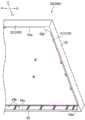
图1是从前侧观察的根据本发明实施例的电子设备的上面的透视图。FIG. 1 is a perspective view of an upper side of an electronic device according to an embodiment of the present invention viewed from the front side.
图2是该电子设备的前视立面图。Fig. 2 is a front elevational view of the electronic device.
图3是该电子设备的俯视平面图。Fig. 3 is a top plan view of the electronic device.
图4是该电子设备的侧视立面图。Fig. 4 is a side elevational view of the electronic device.
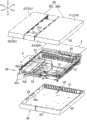
图5是设置在该电子设备中的下盖、上盖和框架的分解透视图。FIG. 5 is an exploded perspective view of a lower cover, an upper cover, and a frame provided in the electronic device.
图6是沿图3中VI-VI线截取的剖面视图。Fig. 6 is a sectional view taken along line VI-VI in Fig. 3 .
图7是沿图3中VII-VII线截取的剖面视图。Fig. 7 is a sectional view taken along line VII-VII in Fig. 3 .
图8是从后侧观察的电子设备的底面的透视图。8 is a perspective view of the bottom surface of the electronic device viewed from the rear side.
图9是下盖的透视图。Fig. 9 is a perspective view of the lower cover.
图10是上盖内侧的透视图。Fig. 10 is a perspective view of the inside of the upper cover.
具体实施方式Detailed ways
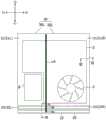
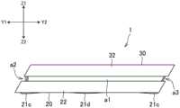
在下文中,参照附图对本发明的实施例进行描述。图1是从前侧观察的根据本发明实施例的电子设备1的上面的透视图。图2是该电子设备1的前视立面图;图3是俯视平面图;而图4是侧视立面图。图5是设置在该电子设备1中的下盖20、上盖30和框架50的分解透视图。图6是沿图3中VI-VI线截取的剖面视图,而图7是沿图3中VII-VII线截取的剖面视图。图8是从后侧观察的电子设备的底面的透视图。图9是下盖20的透视图。图10是上盖30内侧的透视图。在下文的描述中,图1中的附图标记Y1和Y2分别表示向前的方向和向后的方向。X1和X2分别表示向右的方向和向左的方向。Z1和Z2分别表示向上的方向和向下的方向。Hereinafter, embodiments of the present invention are described with reference to the accompanying drawings. FIG. 1 is a perspective view of an upper side of an
电子设备1是用作游戏设备或音频/视频设备的娱乐设备。电子设备1从例如光盘等记录介质获取游戏程序或视频/音频数据。电子设备1具备有线通信功能和/或无线通信功能。由此,在不同的示例中,电子设备1利用通信功能获取游戏程序或视频/音频数据。电子设备1将通过执行游戏程序所产生的动画数据或获取的视频/音频数据输出到显示设备,例如电视机。The
在电子设备1的前面设置有插入槽52c,光盘插入其中(参见图2)。另外,在电子设备1的前面还设置有连接器7,用于连接游戏控制器、外部设备或类似设备。在图2的示例中,前面设置有两个连接器7。应该指出的是,插入槽52c和连接器7并不是必须设置。如图3所示,电子设备1具有:电路板2,其上安装有集成电路例如CPU和存储器;冷却风扇3,用于吸入外部空气;供电单元(未示出)以及其他。电路板2上的集成电路和供电单元由冷却风扇3形成的空气气流进行冷却。An
电子设备1的外部形式大致为平行六面体的形状,具有六个面,其中的每一个面具有四边形形状,且每两个相对的面基本上彼此平行地延伸。特别地,电子设备1的上面和底面基本上彼此平行地延伸;同样,前面和背面基本上彼此平行地延伸;同样,左侧面和右侧面基本上彼此平行地延伸。左侧面和右侧面是平面的。因此,电子设备1可以选择性地设置为其中底面位于下侧的水平放置和侧面位于下侧的铅直放置。从侧视立面图(参见图4)的角度看,此处描述的示例的电子设备1具有大致平行四边形的形状。电子设备1的其他面各自具有大致矩形的形状。The external form of the
电子设备1包括下盖20和上盖30,它们形成外部轮廓。在此处描述的示例中,上盖30包括右上盖30R和左上盖30L,右上盖30R和左上盖30L在左右方向上可以相互隔开(参见图5)。电子设备1包括框架50,内设于电子设备1中的各种部件和装置例如电路板2和冷却风扇3安装于该框架(参见附图5)。下盖20覆盖框架50的下侧并装接于框架50。上盖30覆盖框架50的上侧并装接于框架50。框架50限定出一空间,电子设备1的内设装置放置在该空间内。例如,冷却风扇3放置在空间S1中。同时,光盘驱动器设置在插入槽52c的后侧,且框架50覆盖该光盘驱动器。框架50由例如树脂模制而成。The
如图1所示,用于彼此贯通地连通电子设备1的内部与外部的多个通气孔h设置在电子设备1的侧面上。此处描述的示例的通气孔h是吸入空气的孔。当冷却风扇3被驱动时,空气经由通气孔h被吸入到电子设备1的内部。槽a1形成在电子设备1的侧面,从而在前后方向上延伸。在此处描述的示例中,单一的槽a1形成在该侧面上。槽a1在上下方向上经过该侧面的中心,与电子设备1的上面和底面大致平行地延伸。As shown in FIG. 1 , a plurality of vent holes h for communicating the inside and outside of the
多个通气孔h形成在槽a1的内面上,并在槽a1的延伸方向(在前后方向)上并排设置。形成在侧面上的多个通气孔h的所有通气孔或大部分通气孔位于槽a1内。换句话说,多个通气孔h的位置集中在槽a1内。在图1的示例中,所有多个通气孔h形成在槽a1的内面上,同时没有通气孔h形成在侧面的其他部位。根据所描述的构造,即使在电子设备被铅直放置时,通气孔h也不会封死,并因此电子设备1铅直放置时吸入效率的降低可以被消除。槽a1和通气孔h形成在电子设备1的左和右两个侧面上。另外,通气孔h也可只形成在侧面的其中之一上。A plurality of ventilation holes h are formed on the inner surface of the groove a1 and are arranged side by side in the extending direction of the groove a1 (in the front-rear direction). All or most of the ventilation holes h of the plurality of ventilation holes formed on the side are located in the groove a1. In other words, the positions of the plurality of vent holes h are concentrated in the groove a1. In the example of FIG. 1 , all of the plurality of vent holes h are formed on the inner face of the groove a1 , while none of the vent holes h are formed on other parts of the side. According to the described configuration, even when the
如图1所示,槽a1延伸至电子设备1侧面的前缘b1。槽a1在其前端向前开口。另外,槽a1延伸至电子设备1侧面的后缘c1。槽a1在其后端向后开口。采用所述的结构,当电子设备1被铅直放置时,空气通过槽a1的前端至后端流入槽a1。该空气经由通气孔h被吸入电子设备1内。As shown in FIG. 1 , the groove a1 extends to the front edge b1 of the side of the
如图4所示,电子设备1的前面和背面相对于铅直平面倾斜。特别地,前面从底面向上延伸并向后侧倾斜。背面从底面向上延伸并向后侧倾斜。因此,即使电子设备1被容放在支架或类似物上这样的小地方,也能在前面的前侧和背面的后侧形成空间。由此,通过槽a1的前端和后端流入槽a1的气得以顺畅进行。As shown in FIG. 4 , the front and back of the
如图6所示,框架50具有侧壁部51,沿着电子设备1的侧面延伸。突出部51a和51b形成在侧壁部51上,从而它们向侧方突出并在上下方向上彼此相对。突出部51a和51b在前后方向上延伸。槽a1由侧壁部51和突出部51a和51b构造而成。通气孔h形成在突出部51a和51b中。通气孔h不形成在侧壁部51中。As shown in FIG. 6 , the
换句话说,槽a1的内面具有在上下方向上彼此相对的两个面。特别地,槽a1包括由突出部51a形成的第一面和由突出部51b形成的第二面。槽a1的内面还包括将第一面和第二面相互连接的第三面(由侧壁部51形成的面)。通气孔h形成在第一面和第二面中。采用所述的结构,可以避免通气孔h从电子设备1的外观上突出。通气孔h可以仅形成在下侧的突出部51a(第一面)和上侧的突出部51b(第二面)之一上。In other words, the inner face of the groove a1 has two faces facing each other in the up-down direction. In particular, the groove a1 includes a first face formed by the protruding
在上述的突出部51a和51b的端缘,分别形成安装壁部51c和51d以在前后方向上延伸。安装壁部51c相对于突出部51a朝向槽a1的相对侧(下侧)突出。类似地,安装壁部51d相对于突出部51b朝向槽a1的相对侧(上侧)突出。At the end edges of the above-mentioned
下盖20包括构成电子设备1底面的底面部21,和构成电子设备1侧面的侧面部22。在侧面部22上没有形成通气孔,并且侧面部22具有平坦的外面。突出部51a和安装壁部51c设置在下盖20的底面部21和侧面部22的内侧。侧面部22沿着安装壁部51c设置,并通过多个结合部22a安装在安装壁部51c上,结合部22a形成在侧面部22的内面上并在前后方向上并排设置。在图6的示例中,结合部22a是凸起。安装壁部51c上形成有多个孔或凹部。结合部22a配装在形成在安装壁部51c上的孔或凹部中。The
上盖30包括构成电子设备1上面的上面部31,和构成电子设备1侧面的侧面部32。在侧面部32上没有形成通气孔,并且侧面部32具有平坦的外面。突出部51b和安装壁部51d设置在上面部31和侧面部32的内侧。侧面部32沿着安装壁部51d设置,并通过多个结合部32a安装在安装壁部51d上,结合部32a形成在侧面部32的内面上。在图6的示例中,结合部32a是凸起。安装壁部51d上具有有多个孔或凹部。结合部32a配装在形成在安装壁部51d上的孔或凹部中。The
槽a1的结构不限于以上所述。例如,突出部51a可以与下盖20一体形成,突出部51b可以与上盖30一体形成。The structure of the groove a1 is not limited to the above. For example, the
如图6所示,突出部51a包括将相邻两个通气孔h分隔开的壁部51e。壁部51e朝向与上下方向相正交的方向。在此处描述的示例中,壁部51e相对于前后方向倾斜地设置。壁部51e的铅直尺寸设置为使得电子设备1的内部不会被暴露于外部。As shown in FIG. 6, the protruding
电子设备1在其前面形成有槽a2,从而在左右方向上延伸。槽a2经过前面在上下方向上的中心。如上所述,插入槽52c和连接器7设置在前面上。插入槽52c和连接器7位于槽a2中并在左右方向上并排设置。由此,插入槽52c和连接器7不那么可能从电子设备1的外观突出。而且,灰尘不易进入连接器7或插入槽52c。槽a2从前面的右端延伸至左端。槽a2在其端部连接至形成在侧面上的槽a1。The
如图7所示,框架50包括沿电子设备1前面设置的前壁部52。前壁部52上形成有用于经由其暴露连接器7的孔和插入槽52c。下盖20具有前面部23,该前面部23从底面部21的前缘向上延伸并构成电子设备1的前面。前面部23相对于前壁部52位于前侧。突出部23a形成在前面部23的上缘并朝向前壁部52延伸。上盖30具有前面部33,该前面部33从上面部31的前缘向下延伸,并构成电子设备1的前面。前面部33相对于前壁部52位于前侧。突出部33a还形成在前面部33的下缘并朝向前壁部52延伸。突出部23a和33a在上下方向上彼此相对。槽a2由突出部23a、33a和前壁部52限定。特别地,槽a2的内面包括在上下方向上彼此相对的第一面和第二面,以及将第一面和第二面相互连接的第三面,类似于槽a1。第一面和第二面分别由突出部23a和33a形成,而第三面由前壁部52形成。插入槽52c和将连接器7暴露于外部的孔形成在槽a2的第三面上。此处描述的示例中的前面部23向后侧倾斜。另外,前面部33向下延伸并向前侧倾斜。前面部23和33跨越槽a2而位于彼此相对的两侧,且构成同一平面。As shown in FIG. 7 , the
用作通气孔(在此处描述的示例中,用于吸入空气的孔)的间隙C形成在前壁部52和突出部23a、33a的边缘之间。当冷却风扇3被驱动时,空气经由间隙C被吸入。换句话说,通气孔不但设置在槽a1的内面而且还设置于槽a2的内面。A gap C serving as a vent hole (in the example described here, a hole for sucking in air) is formed between the
在前壁部52上形成有确保间隙C的多个肋52a和52b。肋52a从前壁部52朝向前面部23和底面部21突出。肋52b从前壁部52朝向前面部33突出。A plurality of
前壁部52向上延伸超过突出部33a的位置。另外,前壁部52向下延伸超过突出部23a的位置。因此,可以防止电子设备1的内部经由间隙C外露。应指出的是,间隙C并不是必须设置。在这种情况下,突出部23a和33a可以形成在前壁部52上。The
如图9所示,形成在下盖20前面部23上的突出部23a延伸至侧面部22的前端的上缘。特别是,突出部23a的端部23b设置在侧面部22的上缘和前面部23的上缘之间的拐角处。突出部23a的端部23b从该拐角朝向框架50延伸。另外,本示例中的下盖20具有背面部24,下文将进行详细描述。突出部24a也形成在背面部24的上缘。突出部24a延伸至侧面部22的后端的上缘,而突出部24a的端部24d设置在侧面部22的上缘和背面部24的上缘之间的拐角处。换句话说,下盖20的上缘的四个拐角中的每一个处均设置有突出部。四个拐角处的突出部作为整体围绕框架50。位于拐角处的突出部和框架50的突出部51a一起,构成槽a1的第一面。采用上述的结构,即使在下盖20和框架50之间的拐角处生成空隙,该空隙也不大可能突出,因此可以便利地确保了良好的外观。另外,也可以便利地确保前面部23、侧面部22和背面部24的刚性。As shown in FIG. 9 , the protruding
与下盖20类似地,上盖30也在其每一个拐角处具有突出部。特别是,如图10所示,前面部33的突出部33a延伸至侧面部32的前端的下缘。更特别的是,突出部33a的端部33b设置在侧面部32的下缘和前面部33的下缘之间的拐角处。另外,如下文详细描述地,上盖30具有背面部34。突出部34a也形成在背面部34的下缘。突出部34a延伸至侧面部32的后端的下缘,而突出部34a的端部34d设置在侧面部32的下缘和背面部34的下缘之间的拐角处。换句话说,上盖30的下缘的四个拐角中的每一个处均设置有突出部。位于拐角处的突出部和框架50的突出部51b一起,构成槽a1的第二面。采用上述的结构,即使在上盖30和框架50之间的拐角处生成空隙,该空隙也不大可能突出,因此可以便利地确保良好的外观。另外,也可以便利地确保前面部33、侧面部32和背面部34的刚性。Similar to the
如图1所示,电子设备1的前面设置有按键9a和9b。按键9a和9b其中一个是,例如,电源按键,而另一个是,例如,光盘弹出键。按键9a位于槽a2的下侧,而按键9b位于槽a2的上侧。按键9a和9b不从电子设备1的前面向前突出。特别是,按键9a和9b的前面位于与前面部23、33构成的平面相同的平面上,或从前面部23、33构成的平面稍微靠后一些。如上所述,电子设备1的前面朝向后侧倾斜。因此,可以防止按键9a和9b成为盲点。例如,即使在电子设备1被铅直放置而电子设备1的底面抵靠在支架的内面上的情况下,由于电子设备1的前面倾斜,使用者仍能够看到按键9a和9b。As shown in FIG. 1 ,
一槽形成在下盖20的前面部23,从而在上下方向上延伸。按键9a是铅直细长的部件,并设置在前面部23的槽内。另一槽也形成在上盖30的前面部33从而在上下方向上延伸。按键9b是铅直细长的部件,并设置在前面部33的槽内。前面部33的槽位于前面部23的槽的延长部分上。换句话说,下盖20的槽在左右方向上的位置与上盖30的槽在左右方向上的位置相互重合。A groove is formed in the
如上所述,上盖30包括可以在左右方向上彼此隔开的左上盖30L和右上盖30R。在图5的示例中,结合部31c和31d分别形成在左上盖30L的右边缘和右上盖30R的左边缘,从而结合部31c和31d相互接合。例如,结合部31c和31d其中之一具有被另一结合部卡住的弹簧部。As described above, the
在耦接的状态下一槽形成在左上盖30L和右上盖30R之间。特别是,其中设置有按键9b的上述槽形成在左上盖30L的前面部33L和右上盖的前面部33R之间。A groove is formed between the upper
槽a4(图1)形成在左上盖30L的上面部31L和右上盖30R的上面部31R之间,从而它在前后方向上延伸。上面部31L和31R之间的槽从上面部31L和31R的前缘延伸至后缘。槽a4在其前端与前面部33L和33R之间的槽相连接。在上面部31L和31R之间的槽a4内可设置用于指示电子设备1的操作状态(例如,电源的开/关状态)的指示器。特别是,在上面部31L和31R之间的槽a4内可设置发光元件,用于发射代表电子设备1的操作状态的某种颜色的光。A groove a4 ( FIG. 1 ) is formed between the
在此描述的示例中,设置在电子设备1的前面和上面的上述槽进一步延伸至背面和底面并围绕整个电子设备1。特别是,槽a5形成在下盖20的底面部21,从而它在前后方向上延伸,如图8所示。底面部21的槽a5在其前端与设置有按键9a槽相连接。在下文描述的下盖20的背面部24上形成有槽a6,其从底面部21的槽a5延伸。另外,在下文描述的上盖30的背面部34上形成有槽a7,其从上面部31的槽a4延伸。In the example described here, the above-mentioned grooves provided on the front and upper surfaces of the
如图8所示,在下盖20的底面部21的槽的前端和后端设置有支撑部21c,它们从底面21稍微突出。当电子设备1被水平放置时,支撑部21c支撑电子设备1。每一个支撑部21c具有与槽5a的宽度相对应的宽度。采用所述构造,支撑部21c不大可能突出。另外,在底面部21的右侧或左侧的边缘上(本示例中,在右缘上)设置有支撑部21d,其从底面部21稍微突出。As shown in FIG. 8 , at the front and rear ends of the groove of the
电子设备1包括可由使用者更换的部件。电子设备1包括作为该部件的例子的硬盘驱动器8(参见附图3和5)。硬盘驱动器8设置在框架50上,被左上盖30L覆盖。如上所述,左上盖30L可与右上盖30R分隔开来。使用者可以通过移除左上盖30L来更换硬盘驱动器8。The
左上盖30L形成电子设备1的四个面。特别是,左上盖30L包括上面部31L、侧面部、前面部33L和背面部34L,如图1所示,并且所述各面部形成电子设备1的上面、侧面、前面和背面。因此,如果左上盖30L被移除,那么框架50将在宽的区域上暴露。因此,提高了更换硬盘驱动器8工作的可操作性。The left
如图8所示,多个连接器设置在电子设备1的背面。连接器6a是电源连接器。连接器6b、6c、6d和6e是,例如,AV端子、用于Ethernet(注册商标)或其他的通信端子、用于连接外部设备的AUX端子等等。连接器6a设置在背面的下侧部,而连接器6b、6c、6d和6e设置在背面的上侧部。如上所述,电子设备1的背面朝向后侧倾斜。因此,可以防止外力作用在与连接器6b、6c、6d和6e连接的缆线的端部。连接器6a、6b、6c、6d和6e设置在背面的左右方向上的一侧上(在此描述的示例中,在右侧上)。当电子设备1被铅直摆放时,其被放置为所述一侧居于下侧。As shown in FIG. 8 , a plurality of connectors are provided on the back of the
如下所述,下盖20和右上盖30R通过背面上的螺钉安装到框架50。同时,左上盖30L之于框架50的安装不使用螺钉,并且可以通过解除结合部31c和31d的接合来移除左上盖30L。换句话说,与下盖20和右上盖30R相比较,左上盖30L可以便利地移除。所有的连接器6a、6b、6c、6d和6e位于相对而言较难移除的盖的内侧(下盖20和右上盖30R的内侧)。As described below, the
多个通气孔p设置在电子设备1的背面(在此描述的示例中,通气孔p是排出空气的孔)。当冷却风扇3被驱动,空气经由通气孔p被排出。如上所述,电子设备1的背面朝向后侧倾斜。因此,即使电子设备1被容放在支架等相对狭窄的地方,由于在背面的后侧形成一空间,空气排出效率的降低可以得到避免。A plurality of vent holes p are provided on the back of the electronic device 1 (in the example described here, the vent holes p are holes for exhausting air). When the cooling
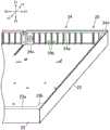
如图8所示,下盖20具有背面部24(参见图9),其从底面部21的后缘向上延伸并朝向后侧倾斜。上盖30具有背面部34(参见图10),其从上面部31的后缘向下延伸并朝向前侧倾斜。框架50具有后壁部53(参见图5),其位于背面部24和34的内侧并沿背面部24和34设置。框架50的后壁部53上形成有通气孔p。每两个相邻的通气孔p由隔栅53a分隔开。用于暴露通气孔p或连接器6b、6c、6d和6e的孔口24b和34b(参见图9和10)分别形成在盖20和30的背面部24和34。As shown in FIG. 8 , the
通过在上盖30和下盖20上分别设置背面部24和34,可以增加上盖30和下盖20的刚性。如图10所示,突出部34a形成在背面部34的下缘,从而其向后壁部53延伸。如图9所示,突出部24a形成在背面部24的上缘,从而其向后壁部53延伸。背面部34的突出部34a和背面部24的突出部24a在上下方向上彼此相对。由此,在电子设备1的背面,槽a3(参见图4)由两个突出部24a、34a和后壁部53形成。换句话说,槽a3的内面包括在上下方向上彼此相对的第一面和第二面,以及将第一面和第二面相互连接的第三面,与槽a1类似。第一面和第二面分别由突出部24a和34a形成,而第三面由后壁部53形成。多个通气孔p形成在第三面上。槽a3在其左右端部连接至形成在侧面上的槽a1。换句话说,一系列槽a1、a2和a3形成在电子设备1的整个周边。应该指出的是,背面的槽a3并不是必须设置。Rigidity of the
在电子设备1上形成通气孔h和p、用于暴露连接器7的孔口、以及用于记录介质的插入槽52c。所述孔和孔口形成在槽a1、a2和a3的内面上。尤其是在电子设备1的侧面和前面上,通气孔h、用于暴露连接器7的孔口、以及用于记录介质的插入槽52c的位置集中在槽a1和a2内。采用所述的结构,与其中孔和孔口的位置散部在电子设备1外面上的其他结构相比较,很容易保证电子设备1的外部部件的刚性。在本示例中,通气孔h、用于暴露连接器7的孔口、以及用于记录介质的插入槽52c都形成在框架50上。因此,很容易保证作为外部部件的盖20和30的刚性。另外,按键9a和9b和指示器设置在前面上形成的槽和上面上形成的槽a4内。换句话说,按键9a和9b和指示器也整合在相对小的区域内。因此。与散部在电子设备1外面上的其他结构相比较,可以便利地保证外部部件的刚性。Vent holes h and p, an aperture for exposing the
如图9所示,在下盖20的背面部24上形成有孔口24c,用于将下盖20固定到框架50的螺钉有待插入所述孔口24c。如上所述,用于将下盖20装接到框架50的侧壁部51的结合部22a形成在下盖20的左和右侧面部22上。在右上盖30R的背面部34R上形成有孔口34c(参见图8),用于将右上盖30R固定到框架50的螺钉有待插入所述孔口34c。设置在右上盖30R左缘上的结合部31d也通过螺钉安装到框架50。同时,左上盖30L之于框架50的安装不使用螺钉。特别是,左上盖30L通过与右上盖30R接合的结合部31c以及在左上盖30L的侧面部形成的结合部32a(参见图6)固定。因此,使用者可以在更换硬盘驱动器8的时候,通过解除结合部31c和结合部32a的接合来移除左上盖30L。As shown in FIG. 9 ,
如上所述,采用电子设备1,槽a1形成在侧面上,设置在该侧面上的多个通气孔h形成在槽a1内。因此,即使当电子设备被铅直放置时,也避免了通气孔h封死,并因此通气效率的降低也得到避免。As described above, with the
应当指出的是,本发明不限于上述电子设备1而是允许各种替代装置。It should be noted that the present invention is not limited to the
例如,在侧面上的槽a1内,可以设置用于排出空气的孔作为通气孔。For example, in the groove a1 on the side surface, a hole for exhausting air may be provided as a vent hole.
框架50并不是必须设置。在这种情况下,上盖30和下盖20可以互相联合以形成盒状的外壳。The
上盖30并不一定要被分隔成左上盖30L和右上盖30R。The
电子设备1在侧视立面图中观察时并不一定要具有平行四边形的形状。例如,电子设备1在侧视立面图中观察时可以具有大致矩形的形状。The
Claims (9)
Priority Applications (1)
| Application Number | Priority Date | Filing Date | Title |
|---|---|---|---|
| CN201910030915.XACN110083212B (en) | 2013-05-17 | 2014-05-07 | Electronic equipment |
Applications Claiming Priority (5)
| Application Number | Priority Date | Filing Date | Title |
|---|---|---|---|
| JP2013-105607 | 2013-05-17 | ||
| JP2013105607 | 2013-05-17 | ||
| CN201480026516.1ACN105229558B (en) | 2013-05-17 | 2014-05-07 | Electronic equipment |
| PCT/JP2014/062250WO2014185310A1 (en) | 2013-05-17 | 2014-05-07 | Electronic device |
| CN201910030915.XACN110083212B (en) | 2013-05-17 | 2014-05-07 | Electronic equipment |
Related Parent Applications (1)
| Application Number | Title | Priority Date | Filing Date |
|---|---|---|---|
| CN201480026516.1ADivisionCN105229558B (en) | 2013-05-17 | 2014-05-07 | Electronic equipment |
Publications (2)
| Publication Number | Publication Date |
|---|---|
| CN110083212A CN110083212A (en) | 2019-08-02 |
| CN110083212Btrue CN110083212B (en) | 2023-07-14 |
Family
ID=51898289
Family Applications (2)
| Application Number | Title | Priority Date | Filing Date |
|---|---|---|---|
| CN201910030915.XAActiveCN110083212B (en) | 2013-05-17 | 2014-05-07 | Electronic equipment |
| CN201480026516.1AActiveCN105229558B (en) | 2013-05-17 | 2014-05-07 | Electronic equipment |
Family Applications After (1)
| Application Number | Title | Priority Date | Filing Date |
|---|---|---|---|
| CN201480026516.1AActiveCN105229558B (en) | 2013-05-17 | 2014-05-07 | Electronic equipment |
Country Status (5)
| Country | Link |
|---|---|
| US (4) | US9832908B2 (en) |
| EP (1) | EP2998825B1 (en) |
| JP (1) | JP6055090B2 (en) |
| CN (2) | CN110083212B (en) |
| WO (1) | WO2014185310A1 (en) |
Families Citing this family (14)
| Publication number | Priority date | Publication date | Assignee | Title |
|---|---|---|---|---|
| PH25408A (en) | 1988-03-11 | 1991-07-01 | Enzyme Bio Systems Ltd | Method for retarding staling of baking products |
| CN110083212B (en)* | 2013-05-17 | 2023-07-14 | 索尼电脑娱乐公司 | Electronic equipment |
| JP6585368B2 (en)* | 2015-04-03 | 2019-10-02 | 株式会社ソニー・インタラクティブエンタテインメント | Electronics |
| FR3042327B1 (en)* | 2015-10-07 | 2019-08-02 | Guillemot Corporation | COOLING SYSTEM OF AN ELECTRIC MOTOR |
| DE102015119364B4 (en) | 2015-11-10 | 2022-05-12 | Andreas Fischer | HOUSING FOR AN ELECTRICAL AND/OR ELECTRONIC COMPONENT |
| JP6538607B2 (en)* | 2016-03-31 | 2019-07-03 | 株式会社ソニー・インタラクティブエンタテインメント | Electronics |
| CA3090944A1 (en) | 2017-02-08 | 2018-08-16 | Upstream Data Inc. | Blockchain mine at oil or gas facility |
| JP2019102545A (en)* | 2017-11-29 | 2019-06-24 | 株式会社デンソー | Electronic device |
| WO2019181804A1 (en) | 2018-03-22 | 2019-09-26 | 株式会社ソニー・インタラクティブエンタテインメント | Electronic apparatus |
| USD920330S1 (en)* | 2018-04-18 | 2021-05-25 | Seagate Technology Llc | Storage device |
| CA3139776A1 (en) | 2019-05-15 | 2020-11-19 | Upstream Data Inc. | Portable blockchain mining system and methods of use |
| CA3076653A1 (en) | 2020-03-21 | 2021-09-21 | Upstream Data Inc. | Portable blockchain mining systems and methods of use |
| JP2022185414A (en)* | 2021-06-02 | 2022-12-14 | キオクシア株式会社 | semiconductor storage device |
| EP4149224A1 (en) | 2021-09-09 | 2023-03-15 | Stryker European Operations Limited | Housing assembly for accommodating printed circuit boards |
Citations (4)
| Publication number | Priority date | Publication date | Assignee | Title |
|---|---|---|---|---|
| CN1327711A (en)* | 1999-09-06 | 2001-12-19 | 索尼计算机娱乐公司 | Electronic device and case for said electronic device |
| JP2008010769A (en)* | 2006-06-30 | 2008-01-17 | Toshiba Corp | Information recording / reproducing device |
| CN201751662U (en)* | 2010-07-23 | 2011-02-23 | 陈音奇 | Heat radiation seat for notebook computer |
| CN105229558B (en)* | 2013-05-17 | 2019-08-16 | 索尼电脑娱乐公司 | Electronic equipment |
Family Cites Families (78)
| Publication number | Priority date | Publication date | Assignee | Title |
|---|---|---|---|---|
| DE3603915A1 (en) | 1986-02-07 | 1987-08-13 | Siemens Ag | Instrument case |
| JPH062317Y2 (en)* | 1988-08-09 | 1994-01-19 | 株式会社東芝 | Case structure |
| US5339362A (en)* | 1992-01-07 | 1994-08-16 | Rockford Corporation | Automotive audio system |
| JP2577674Y2 (en)* | 1992-06-09 | 1998-07-30 | アルパイン株式会社 | Automotive electronics |
| JPH06188581A (en)* | 1992-12-16 | 1994-07-08 | Ricoh Co Ltd | Heat dissipation structure for electronic devices |
| DE9300661U1 (en) | 1993-01-20 | 1993-03-04 | Mannesmann Kienzle GmbH, 7730 Villingen-Schwenningen | Housing for an electronic device |
| JPH06314139A (en) | 1993-04-30 | 1994-11-08 | Toshiba Corp | Portable electronic devices |
| JPH0784673A (en) | 1993-09-09 | 1995-03-31 | Toshiba Corp | Portable electronic device and assembling method thereof |
| JPH10270879A (en) | 1997-03-26 | 1998-10-09 | Toshiba Corp | Electronic equipment cooling structure |
| JPH10307637A (en) | 1997-05-07 | 1998-11-17 | Toshiba Corp | Portable electronic devices |
| JP2001148578A (en) | 1999-09-06 | 2001-05-29 | Sony Computer Entertainment Inc | Electronic equipment housing and electronic equipment |
| JP2001210981A (en)* | 2000-01-28 | 2001-08-03 | Nintendo Co Ltd | Electronic appliance having radiating structure, and television-game machine having the radiating structure |
| JP2002132387A (en)* | 2000-10-25 | 2002-05-10 | Sony Computer Entertainment Inc | Control method for cooling fan and information processor |
| JP2002185157A (en) | 2000-12-13 | 2002-06-28 | Sony Corp | Case of high-frequency device |
| US6538886B2 (en)* | 2001-04-18 | 2003-03-25 | Chung Che Yu | Hard disk driver casing bottom-mounted heat sink |
| US6900984B2 (en)* | 2001-04-24 | 2005-05-31 | Apple Computer, Inc. | Computer component protection |
| JP3652634B2 (en)* | 2001-10-05 | 2005-05-25 | 本田技研工業株式会社 | Cooling structure for high piezoelectric parts |
| JP2003218545A (en)* | 2002-01-23 | 2003-07-31 | Seiko Epson Corp | Exterior case for electronic equipment, projector equipped with this exterior case for electronic equipment |
| US6914779B2 (en)* | 2002-02-15 | 2005-07-05 | Microsoft Corporation | Controlling thermal, acoustic, and/or electromagnetic properties of a computing device |
| JP4382511B2 (en)* | 2004-02-05 | 2009-12-16 | パイオニア株式会社 | Conduction device |
| US7068516B2 (en)* | 2004-02-06 | 2006-06-27 | Chan Eric K D | Enclosure with pre-formed interchangeable panels |
| JP2005331945A (en) | 2004-05-18 | 2005-12-02 | Samsung Sdi Co Ltd | Plasma display device |
| JP2006156501A (en)* | 2004-11-25 | 2006-06-15 | Orion Denki Kk | Electronic device with housing |
| JP2006179712A (en)* | 2004-12-22 | 2006-07-06 | Toshiba Corp | Electronic device and display device using the same |
| US8009426B2 (en)* | 2005-11-23 | 2011-08-30 | Comcast Cable Holdings Llc | Housing for protecting electronic components having vents |
| JP4675283B2 (en) | 2006-06-14 | 2011-04-20 | トヨタ自動車株式会社 | Heat sink and cooler |
| US7733659B2 (en)* | 2006-08-18 | 2010-06-08 | Delphi Technologies, Inc. | Lightweight audio system for automotive applications and method |
| US7898806B2 (en) | 2006-09-04 | 2011-03-01 | Kabushiki Kaisha Yaskawa Denki | Motor controller |
| US7817421B2 (en) | 2006-09-13 | 2010-10-19 | Kabushiki Kaisha Yaskawa Denki | Motor controller |
| JP4699967B2 (en) | 2006-09-21 | 2011-06-15 | 株式会社ソニー・コンピュータエンタテインメント | Information processing device |
| US8004837B2 (en)* | 2006-10-13 | 2011-08-23 | Kabushiki Kaisha Yaskawa Denki | Control device |
| US8498117B2 (en) | 2006-11-16 | 2013-07-30 | Advanced Micro Devices, Inc. | Variable mount voltage regulator |
| JP2008162479A (en)* | 2006-12-28 | 2008-07-17 | Sony Corp | On-vehicle equipment |
| JP2008197392A (en)* | 2007-02-13 | 2008-08-28 | Sharp Corp | Thin display device |
| JP2008270485A (en) | 2007-04-19 | 2008-11-06 | Toyota Industries Corp | Semiconductor device |
| ES2504515T3 (en) | 2007-05-25 | 2014-10-08 | Sma Solar Technology Ag | Investor Housing |
| TWM328610U (en) | 2007-09-14 | 2008-03-11 | Touch Electronic Co Ltd | Power supply heat dissipation structure |
| DE102007045733B3 (en)* | 2007-09-25 | 2009-02-05 | Qimonda Ag | Memory module comprises board with two sides, where memory chips are arranged on former and latter side, where longitudinally proceeding heat pipe module is arranged on former side |
| KR101407622B1 (en) | 2007-11-09 | 2014-06-13 | 삼성디스플레이 주식회사 | Display device |
| EP2120263A4 (en)* | 2007-11-30 | 2010-10-13 | Panasonic Corp | HEAT DISSIPATING STRUCTURE BASE PLATE, MODULE USING HEAT DISSIPATING STRUCTURE BASE PLATE, AND METHOD FOR MANUFACTURING HEAT DISSIPATING STRUCTURE BASE PLATE |
| JP4857252B2 (en) | 2007-12-07 | 2012-01-18 | 株式会社日立製作所 | Electronics |
| US7742307B2 (en) | 2008-01-17 | 2010-06-22 | Raytheon Company | High performance power device |
| US7796376B2 (en) | 2008-01-17 | 2010-09-14 | Yaskawa America, Inc. | Electrical enclosure cooling structure assembly and method |
| US7961463B2 (en) | 2008-04-02 | 2011-06-14 | Microsoft Corporation | Power efficient data center |
| US8064200B1 (en)* | 2008-04-16 | 2011-11-22 | Cyan Optics, Inc. | Cooling a chassis by moving air through a midplane between two sets of channels oriented laterally relative to one another |
| EP2110929B1 (en)* | 2008-04-18 | 2018-08-29 | Grundfos Management a/s | Frequency inverter being mounted on a motor |
| US7859858B2 (en)* | 2008-05-12 | 2010-12-28 | Cisco Technology, Inc. | Locking hinge design |
| TWM348453U (en)* | 2008-05-19 | 2009-01-01 | Micro Star Int Co Ltd | Display module capable of adjusting location of an opening of an electronic device |
| JP4657329B2 (en)* | 2008-07-29 | 2011-03-23 | 日立オートモティブシステムズ株式会社 | Power converter and electric vehicle |
| US7746639B2 (en) | 2008-10-02 | 2010-06-29 | Raytheon Company | Canister housing |
| JP2010238941A (en)* | 2009-03-31 | 2010-10-21 | Sanyo Electric Co Ltd | Light emitting device |
| JP5378863B2 (en) | 2009-04-02 | 2013-12-25 | 株式会社ソニー・コンピュータエンタテインメント | Electronics |
| DE102009018787A1 (en) | 2009-04-24 | 2010-10-28 | Akasol Engineering Gmbh | battery module |
| EP2299582B1 (en) | 2009-09-18 | 2015-03-11 | SMA Solar Technology AG | Inverter with a housing and electric and electronic components assembled within same |
| WO2011059644A1 (en) | 2009-11-11 | 2011-05-19 | Nextronex Energy Systems, Llc | Inverter system |
| TW201121395A (en) | 2009-12-03 | 2011-06-16 | Hon Hai Prec Ind Co Ltd | Server heat dissipation device and fan module thereof |
| JP4818429B2 (en)* | 2009-12-28 | 2011-11-16 | 株式会社東芝 | Electronics |
| US8164897B2 (en) | 2010-02-19 | 2012-04-24 | International Business Machines Corporation | Airflow recirculation and cooling apparatus and method for an electronics rack |
| JP2011192809A (en)* | 2010-03-15 | 2011-09-29 | Omron Corp | Power conditioner device and module substrate structure using the same |
| US8072756B1 (en) | 2010-05-28 | 2011-12-06 | Rockwell Automation Technologies, Inc. | Air cooling of medium voltage drive components |
| US8243451B2 (en) | 2010-06-08 | 2012-08-14 | Toyota Motor Engineering & Manufacturing North America, Inc. | Cooling member for heat containing device |
| JP2012023329A (en)* | 2010-06-14 | 2012-02-02 | Toshiba Corp | Substrate unit and electronic device |
| JP2012064897A (en)* | 2010-09-17 | 2012-03-29 | Toshiba Corp | Electronic apparatus |
| JP2012069685A (en)* | 2010-09-22 | 2012-04-05 | Panasonic Corp | Electronic apparatus |
| CN102478949B (en) | 2010-11-30 | 2014-10-29 | 英业达股份有限公司 | server |
| JP5483209B2 (en)* | 2011-03-30 | 2014-05-07 | 株式会社安川電機 | Power converter |
| JP5161992B2 (en)* | 2011-03-31 | 2013-03-13 | 株式会社東芝 | Electronics |
| JP5383740B2 (en)* | 2011-04-18 | 2014-01-08 | 株式会社ソニー・コンピュータエンタテインメント | Electronics |
| JP5236771B2 (en)* | 2011-04-18 | 2013-07-17 | 株式会社ソニー・コンピュータエンタテインメント | Electronics |
| JP2012243961A (en) | 2011-05-19 | 2012-12-10 | Sony Computer Entertainment Inc | Electronic apparatus |
| JP5803327B2 (en) | 2011-06-27 | 2015-11-04 | 富士電機株式会社 | Inverter device waterproof cover |
| CN102852943B (en)* | 2011-06-28 | 2016-08-17 | 富泰华工业(深圳)有限公司 | Lock solid structure and there is the electronic equipment of this lock solid structure |
| JP5638484B2 (en)* | 2011-08-04 | 2014-12-10 | 株式会社ソニー・コンピュータエンタテインメント | Electronics |
| US8902607B1 (en)* | 2011-11-03 | 2014-12-02 | Veex Inc. | Modular electronic testing apparatus and methods |
| JP2013247346A (en)* | 2012-05-29 | 2013-12-09 | Fujitsu Ltd | Outdoor mobile communication base station equipment |
| FR3004062B1 (en)* | 2013-03-27 | 2015-04-24 | Thales Sa | RACK FOR EQUIPPING AERONAUTICAL PLATFORM. |
| JP5805141B2 (en)* | 2013-06-07 | 2015-11-04 | 株式会社ソニー・コンピュータエンタテインメント | Electronics |
| JP5801848B2 (en)* | 2013-06-07 | 2015-10-28 | 株式会社ソニー・コンピュータエンタテインメント | Electronic device stand |
- 2014
- 2014-05-07CNCN201910030915.XApatent/CN110083212B/enactiveActive
- 2014-05-07WOPCT/JP2014/062250patent/WO2014185310A1/enactiveApplication Filing
- 2014-05-07JPJP2015517039Apatent/JP6055090B2/enactiveActive
- 2014-05-07CNCN201480026516.1Apatent/CN105229558B/enactiveActive
- 2014-05-07EPEP14797356.4Apatent/EP2998825B1/enactiveActive
- 2014-05-07USUS14/891,677patent/US9832908B2/enactiveActive
- 2017
- 2017-03-23USUS15/466,877patent/US9955593B2/enactiveActive
- 2018
- 2018-03-30USUS15/941,158patent/US10791634B2/enactiveActive
- 2020
- 2020-08-27USUS17/004,859patent/US11013129B2/enactiveActive
Patent Citations (4)
| Publication number | Priority date | Publication date | Assignee | Title |
|---|---|---|---|---|
| CN1327711A (en)* | 1999-09-06 | 2001-12-19 | 索尼计算机娱乐公司 | Electronic device and case for said electronic device |
| JP2008010769A (en)* | 2006-06-30 | 2008-01-17 | Toshiba Corp | Information recording / reproducing device |
| CN201751662U (en)* | 2010-07-23 | 2011-02-23 | 陈音奇 | Heat radiation seat for notebook computer |
| CN105229558B (en)* | 2013-05-17 | 2019-08-16 | 索尼电脑娱乐公司 | Electronic equipment |
Also Published As
| Publication number | Publication date |
|---|---|
| US20170196098A1 (en) | 2017-07-06 |
| JPWO2014185310A1 (en) | 2017-02-23 |
| EP2998825A1 (en) | 2016-03-23 |
| JP6055090B2 (en) | 2016-12-27 |
| US20180228035A1 (en) | 2018-08-09 |
| US10791634B2 (en) | 2020-09-29 |
| US20200396848A1 (en) | 2020-12-17 |
| EP2998825B1 (en) | 2018-11-28 |
| US9955593B2 (en) | 2018-04-24 |
| CN110083212A (en) | 2019-08-02 |
| CN105229558A (en) | 2016-01-06 |
| EP2998825A4 (en) | 2017-03-01 |
| WO2014185310A1 (en) | 2014-11-20 |
| US20160120061A1 (en) | 2016-04-28 |
| US11013129B2 (en) | 2021-05-18 |
| CN105229558B (en) | 2019-08-16 |
| US9832908B2 (en) | 2017-11-28 |
Similar Documents
| Publication | Publication Date | Title |
|---|---|---|
| CN110083212B (en) | Electronic equipment | |
| US9629274B2 (en) | Electronic apparatus and fabrication method therefor | |
| JP5805141B2 (en) | Electronics | |
| JP5314481B2 (en) | Electronics | |
| US20090147477A1 (en) | Electronic device | |
| CN107806672B (en) | Air conditioner outdoor unit | |
| JP5643030B2 (en) | Projection display | |
| JP5801848B2 (en) | Electronic device stand | |
| CN104244638A (en) | Electronic apparatus | |
| JP5882818B2 (en) | Electronics | |
| TW201328493A (en) | Electronic device enclosure | |
| JP5228006B2 (en) | Game machine | |
| JP5867156B2 (en) | Air conditioner | |
| JP7062048B2 (en) | Electronics | |
| KR100561746B1 (en) | TV chiller |
Legal Events
| Date | Code | Title | Description |
|---|---|---|---|
| PB01 | Publication | ||
| PB01 | Publication | ||
| SE01 | Entry into force of request for substantive examination | ||
| SE01 | Entry into force of request for substantive examination | ||
| GR01 | Patent grant | ||
| GR01 | Patent grant |