CN110073584B - Hybrid secondary side regulation - Google Patents
Hybrid secondary side regulationDownload PDFInfo
- Publication number
- CN110073584B CN110073584BCN201880004926.4ACN201880004926ACN110073584BCN 110073584 BCN110073584 BCN 110073584BCN 201880004926 ACN201880004926 ACN 201880004926ACN 110073584 BCN110073584 BCN 110073584B
- Authority
- CN
- China
- Prior art keywords
- power switch
- controller
- primary
- voltage
- switch
- Prior art date
- Legal status (The legal status is an assumption and is not a legal conclusion. Google has not performed a legal analysis and makes no representation as to the accuracy of the status listed.)
- Active
Links
- 238000000034methodMethods0.000claimsabstractdescription17
- 238000004804windingMethods0.000claimsdescription44
- 230000006854communicationEffects0.000claimsdescription14
- 238000004891communicationMethods0.000claimsdescription14
- 230000001351cycling effectEffects0.000claimsdescription10
- 230000008569processEffects0.000claimsdescription7
- 230000004044responseEffects0.000claimsdescription6
- 238000001514detection methodMethods0.000abstractdescription9
- 238000012545processingMethods0.000description5
- 239000003990capacitorSubstances0.000description4
- 210000003127kneeAnatomy0.000description4
- 230000002159abnormal effectEffects0.000description3
- 230000000694effectsEffects0.000description3
- 238000002955isolationMethods0.000description3
- 238000012986modificationMethods0.000description3
- 230000004048modificationEffects0.000description3
- 230000001105regulatory effectEffects0.000description3
- 230000007704transitionEffects0.000description3
- WHXSMMKQMYFTQS-UHFFFAOYSA-NLithiumChemical compound[Li]WHXSMMKQMYFTQS-UHFFFAOYSA-N0.000description2
- 230000008901benefitEffects0.000description2
- 238000013461designMethods0.000description2
- 229910052744lithiumInorganic materials0.000description2
- 239000000463materialSubstances0.000description2
- 238000006467substitution reactionMethods0.000description2
- 230000001360synchronised effectEffects0.000description2
- 230000007175bidirectional communicationEffects0.000description1
- 230000002457bidirectional effectEffects0.000description1
- 230000001276controlling effectEffects0.000description1
- 230000008878couplingEffects0.000description1
- 238000010168coupling processMethods0.000description1
- 238000005859coupling reactionMethods0.000description1
- 230000007812deficiencyEffects0.000description1
- 238000010586diagramMethods0.000description1
- 238000001914filtrationMethods0.000description1
- 238000004519manufacturing processMethods0.000description1
- 230000010355oscillationEffects0.000description1
- 230000011664signalingEffects0.000description1
Images

Classifications
- H—ELECTRICITY
- H02—GENERATION; CONVERSION OR DISTRIBUTION OF ELECTRIC POWER
- H02M—APPARATUS FOR CONVERSION BETWEEN AC AND AC, BETWEEN AC AND DC, OR BETWEEN DC AND DC, AND FOR USE WITH MAINS OR SIMILAR POWER SUPPLY SYSTEMS; CONVERSION OF DC OR AC INPUT POWER INTO SURGE OUTPUT POWER; CONTROL OR REGULATION THEREOF
- H02M3/00—Conversion of DC power input into DC power output
- H02M3/22—Conversion of DC power input into DC power output with intermediate conversion into AC
- H02M3/24—Conversion of DC power input into DC power output with intermediate conversion into AC by static converters
- H02M3/28—Conversion of DC power input into DC power output with intermediate conversion into AC by static converters using discharge tubes with control electrode or semiconductor devices with control electrode to produce the intermediate AC
- H02M3/325—Conversion of DC power input into DC power output with intermediate conversion into AC by static converters using discharge tubes with control electrode or semiconductor devices with control electrode to produce the intermediate AC using devices of a triode or a transistor type requiring continuous application of a control signal
- H02M3/335—Conversion of DC power input into DC power output with intermediate conversion into AC by static converters using discharge tubes with control electrode or semiconductor devices with control electrode to produce the intermediate AC using devices of a triode or a transistor type requiring continuous application of a control signal using semiconductor devices only
- H02M3/33507—Conversion of DC power input into DC power output with intermediate conversion into AC by static converters using discharge tubes with control electrode or semiconductor devices with control electrode to produce the intermediate AC using devices of a triode or a transistor type requiring continuous application of a control signal using semiconductor devices only with automatic control of the output voltage or current, e.g. flyback converters
- H02M3/33523—Conversion of DC power input into DC power output with intermediate conversion into AC by static converters using discharge tubes with control electrode or semiconductor devices with control electrode to produce the intermediate AC using devices of a triode or a transistor type requiring continuous application of a control signal using semiconductor devices only with automatic control of the output voltage or current, e.g. flyback converters with galvanic isolation between input and output of both the power stage and the feedback loop
- H—ELECTRICITY
- H02—GENERATION; CONVERSION OR DISTRIBUTION OF ELECTRIC POWER
- H02J—CIRCUIT ARRANGEMENTS OR SYSTEMS FOR SUPPLYING OR DISTRIBUTING ELECTRIC POWER; SYSTEMS FOR STORING ELECTRIC ENERGY
- H02J7/00—Circuit arrangements for charging or depolarising batteries or for supplying loads from batteries
- H02J7/02—Circuit arrangements for charging or depolarising batteries or for supplying loads from batteries for charging batteries from AC mains by converters
- H—ELECTRICITY
- H02—GENERATION; CONVERSION OR DISTRIBUTION OF ELECTRIC POWER
- H02M—APPARATUS FOR CONVERSION BETWEEN AC AND AC, BETWEEN AC AND DC, OR BETWEEN DC AND DC, AND FOR USE WITH MAINS OR SIMILAR POWER SUPPLY SYSTEMS; CONVERSION OF DC OR AC INPUT POWER INTO SURGE OUTPUT POWER; CONTROL OR REGULATION THEREOF
- H02M1/00—Details of apparatus for conversion
- H02M1/32—Means for protecting converters other than automatic disconnection
- H—ELECTRICITY
- H02—GENERATION; CONVERSION OR DISTRIBUTION OF ELECTRIC POWER
- H02M—APPARATUS FOR CONVERSION BETWEEN AC AND AC, BETWEEN AC AND DC, OR BETWEEN DC AND DC, AND FOR USE WITH MAINS OR SIMILAR POWER SUPPLY SYSTEMS; CONVERSION OF DC OR AC INPUT POWER INTO SURGE OUTPUT POWER; CONTROL OR REGULATION THEREOF
- H02M1/00—Details of apparatus for conversion
- H02M1/36—Means for starting or stopping converters
- H—ELECTRICITY
- H02—GENERATION; CONVERSION OR DISTRIBUTION OF ELECTRIC POWER
- H02M—APPARATUS FOR CONVERSION BETWEEN AC AND AC, BETWEEN AC AND DC, OR BETWEEN DC AND DC, AND FOR USE WITH MAINS OR SIMILAR POWER SUPPLY SYSTEMS; CONVERSION OF DC OR AC INPUT POWER INTO SURGE OUTPUT POWER; CONTROL OR REGULATION THEREOF
- H02M3/00—Conversion of DC power input into DC power output
- H02M3/22—Conversion of DC power input into DC power output with intermediate conversion into AC
- H02M3/24—Conversion of DC power input into DC power output with intermediate conversion into AC by static converters
- H02M3/28—Conversion of DC power input into DC power output with intermediate conversion into AC by static converters using discharge tubes with control electrode or semiconductor devices with control electrode to produce the intermediate AC
- H02M3/325—Conversion of DC power input into DC power output with intermediate conversion into AC by static converters using discharge tubes with control electrode or semiconductor devices with control electrode to produce the intermediate AC using devices of a triode or a transistor type requiring continuous application of a control signal
- H02M3/335—Conversion of DC power input into DC power output with intermediate conversion into AC by static converters using discharge tubes with control electrode or semiconductor devices with control electrode to produce the intermediate AC using devices of a triode or a transistor type requiring continuous application of a control signal using semiconductor devices only
- H02M3/33507—Conversion of DC power input into DC power output with intermediate conversion into AC by static converters using discharge tubes with control electrode or semiconductor devices with control electrode to produce the intermediate AC using devices of a triode or a transistor type requiring continuous application of a control signal using semiconductor devices only with automatic control of the output voltage or current, e.g. flyback converters
- H—ELECTRICITY
- H02—GENERATION; CONVERSION OR DISTRIBUTION OF ELECTRIC POWER
- H02M—APPARATUS FOR CONVERSION BETWEEN AC AND AC, BETWEEN AC AND DC, OR BETWEEN DC AND DC, AND FOR USE WITH MAINS OR SIMILAR POWER SUPPLY SYSTEMS; CONVERSION OF DC OR AC INPUT POWER INTO SURGE OUTPUT POWER; CONTROL OR REGULATION THEREOF
- H02M3/00—Conversion of DC power input into DC power output
- H02M3/22—Conversion of DC power input into DC power output with intermediate conversion into AC
- H02M3/24—Conversion of DC power input into DC power output with intermediate conversion into AC by static converters
- H02M3/28—Conversion of DC power input into DC power output with intermediate conversion into AC by static converters using discharge tubes with control electrode or semiconductor devices with control electrode to produce the intermediate AC
- H02M3/325—Conversion of DC power input into DC power output with intermediate conversion into AC by static converters using discharge tubes with control electrode or semiconductor devices with control electrode to produce the intermediate AC using devices of a triode or a transistor type requiring continuous application of a control signal
- H02M3/335—Conversion of DC power input into DC power output with intermediate conversion into AC by static converters using discharge tubes with control electrode or semiconductor devices with control electrode to produce the intermediate AC using devices of a triode or a transistor type requiring continuous application of a control signal using semiconductor devices only
- H02M3/33569—Conversion of DC power input into DC power output with intermediate conversion into AC by static converters using discharge tubes with control electrode or semiconductor devices with control electrode to produce the intermediate AC using devices of a triode or a transistor type requiring continuous application of a control signal using semiconductor devices only having several active switching elements
- H02M3/33576—Conversion of DC power input into DC power output with intermediate conversion into AC by static converters using discharge tubes with control electrode or semiconductor devices with control electrode to produce the intermediate AC using devices of a triode or a transistor type requiring continuous application of a control signal using semiconductor devices only having several active switching elements having at least one active switching element at the secondary side of an isolation transformer
- H02M3/33592—Conversion of DC power input into DC power output with intermediate conversion into AC by static converters using discharge tubes with control electrode or semiconductor devices with control electrode to produce the intermediate AC using devices of a triode or a transistor type requiring continuous application of a control signal using semiconductor devices only having several active switching elements having at least one active switching element at the secondary side of an isolation transformer having a synchronous rectifier circuit or a synchronous freewheeling circuit at the secondary side of an isolation transformer
- H—ELECTRICITY
- H02—GENERATION; CONVERSION OR DISTRIBUTION OF ELECTRIC POWER
- H02J—CIRCUIT ARRANGEMENTS OR SYSTEMS FOR SUPPLYING OR DISTRIBUTING ELECTRIC POWER; SYSTEMS FOR STORING ELECTRIC ENERGY
- H02J2207/00—Indexing scheme relating to details of circuit arrangements for charging or depolarising batteries or for supplying loads from batteries
- H02J2207/20—Charging or discharging characterised by the power electronics converter
- H—ELECTRICITY
- H02—GENERATION; CONVERSION OR DISTRIBUTION OF ELECTRIC POWER
- H02J—CIRCUIT ARRANGEMENTS OR SYSTEMS FOR SUPPLYING OR DISTRIBUTING ELECTRIC POWER; SYSTEMS FOR STORING ELECTRIC ENERGY
- H02J7/00—Circuit arrangements for charging or depolarising batteries or for supplying loads from batteries
- H—ELECTRICITY
- H02—GENERATION; CONVERSION OR DISTRIBUTION OF ELECTRIC POWER
- H02M—APPARATUS FOR CONVERSION BETWEEN AC AND AC, BETWEEN AC AND DC, OR BETWEEN DC AND DC, AND FOR USE WITH MAINS OR SIMILAR POWER SUPPLY SYSTEMS; CONVERSION OF DC OR AC INPUT POWER INTO SURGE OUTPUT POWER; CONTROL OR REGULATION THEREOF
- H02M1/00—Details of apparatus for conversion
- H02M1/0048—Circuits or arrangements for reducing losses
- H02M1/0054—Transistor switching losses
- H02M1/0058—Transistor switching losses by employing soft switching techniques, i.e. commutation of transistors when applied voltage is zero or when current flow is zero
- Y—GENERAL TAGGING OF NEW TECHNOLOGICAL DEVELOPMENTS; GENERAL TAGGING OF CROSS-SECTIONAL TECHNOLOGIES SPANNING OVER SEVERAL SECTIONS OF THE IPC; TECHNICAL SUBJECTS COVERED BY FORMER USPC CROSS-REFERENCE ART COLLECTIONS [XRACs] AND DIGESTS
- Y02—TECHNOLOGIES OR APPLICATIONS FOR MITIGATION OR ADAPTATION AGAINST CLIMATE CHANGE
- Y02B—CLIMATE CHANGE MITIGATION TECHNOLOGIES RELATED TO BUILDINGS, e.g. HOUSING, HOUSE APPLIANCES OR RELATED END-USER APPLICATIONS
- Y02B40/00—Technologies aiming at improving the efficiency of home appliances, e.g. induction cooking or efficient technologies for refrigerators, freezers or dish washers
- Y—GENERAL TAGGING OF NEW TECHNOLOGICAL DEVELOPMENTS; GENERAL TAGGING OF CROSS-SECTIONAL TECHNOLOGIES SPANNING OVER SEVERAL SECTIONS OF THE IPC; TECHNICAL SUBJECTS COVERED BY FORMER USPC CROSS-REFERENCE ART COLLECTIONS [XRACs] AND DIGESTS
- Y02—TECHNOLOGIES OR APPLICATIONS FOR MITIGATION OR ADAPTATION AGAINST CLIMATE CHANGE
- Y02B—CLIMATE CHANGE MITIGATION TECHNOLOGIES RELATED TO BUILDINGS, e.g. HOUSING, HOUSE APPLIANCES OR RELATED END-USER APPLICATIONS
- Y02B70/00—Technologies for an efficient end-user side electric power management and consumption
- Y02B70/10—Technologies improving the efficiency by using switched-mode power supplies [SMPS], i.e. efficient power electronics conversion e.g. power factor correction or reduction of losses in power supplies or efficient standby modes
Landscapes
- Engineering & Computer Science (AREA)
- Power Engineering (AREA)
- Dc-Dc Converters (AREA)
Abstract
Translated fromChinese
Description
Translated fromChinese相关申请的交叉引用CROSS-REFERENCE TO RELATED APPLICATIONS
本申请要求2017年1月12日提交的美国临时申请第62/445,660号的权益。This application claims the benefit of US Provisional Application No. 62/445,660, filed January 12, 2017.
技术领域technical field
本申请涉及开关电源转换器,并且更具体地涉及用于反激转换器的混合次级侧调节方案。The present application relates to switching power converters, and more particularly to hybrid secondary-side regulation schemes for flyback converters.
背景技术Background technique
与线性调节器相比,开关电源转换器提供了更高的效率。虽然线性调节器相对便宜,但是它们通过简单地将差异作为热量燃烧来从较高输入电压调节较低输出电压。结果,线性调节器通常消耗比实际提供给负载的更多的功率。相比之下,开关电源转换器通过电源开关的循环提供相对小的能量增量来调节其输出电压。开关电源转换器中的电源开关不是关闭就是开启,因此与线性调节器相比,效率得到显著提高。因此,诸如反激转换器之类的开关电源转换器通常用于为移动设备的电池充电。Compared to linear regulators, switching power converters offer higher efficiency. Although linear regulators are relatively inexpensive, they regulate lower output voltages from higher input voltages by simply burning the difference as heat. As a result, linear regulators typically consume more power than is actually delivered to the load. In contrast, a switching power converter regulates its output voltage by providing relatively small increments of energy through cycling of the power switch. The power switches in switching power converters are either off or on, resulting in significantly improved efficiency compared to linear regulators. Therefore, switching power converters such as flyback converters are often used to charge the batteries of mobile devices.
反激转换器不仅高效,而且它们的变压器提供正被充电的设备与AC电源的安全隔离。但是该隔离导致调节问题,因为输出电压(或输出电流)是从变压器的次级绕组传递的,而电源开关连接到变压器的初级绕组。因此,控制器的自然位置在初级侧,以通过调节电源开关的循环来调节输出功率输送。但是初级侧控制器不能简单地诸如通过导线或引线直接读取输出电压,因为那样的话,变压器的初级侧和次级侧之间的隔离将被破坏。因此,初级侧控制器通常通过诸如光隔离器之类的隔离通信信道来接收关于输出电压的反馈信息。虽然初级侧控制器然后可以接收反馈信息,但是光隔离器引起稳定性问题并给反激转换器设计增加费用。Not only are flyback converters efficient, but their transformers provide safe isolation of the device being charged from the AC power source. But this isolation causes regulation problems because the output voltage (or output current) is delivered from the secondary winding of the transformer, and the power switch is connected to the primary winding of the transformer. Therefore, the natural location of the controller is on the primary side to regulate the output power delivery by regulating the cycling of the power switch. But the primary side controller cannot simply read the output voltage directly, such as through wires or leads, because then the isolation between the primary and secondary sides of the transformer would be broken. Therefore, the primary side controller typically receives feedback information on the output voltage through an isolated communication channel such as an opto-isolator. While the primary side controller can then receive feedback information, optoisolators cause stability issues and add expense to the flyback converter design.
为了避免这样的稳定性和费用问题,反激转换器设计演变为使用仅初级反馈(primary-only feedback)。在仅初级反馈中,初级侧在次级电流在电源开关的循环之后斜坡下降到零时的时刻感测辅助绕组(或初级绕组)上的电压。该时刻被称为变压器复位时间,并且表示通过辅助绕组电压间接地对输出电压进行采样的理想时间,因为在变压器复位时间在输出电压和辅助绕组电压之间存在线性关系。但是在变压器复位时间之后,辅助绕组电压将开始共振振荡。因此难以在变压器复位时间的精确时刻对辅助绕组电压进行采样。另外,噪声和其他非理想性限制了仅初级反馈的准确性。例如,通过仅初级反馈来调节输出电压的准确性受限于以下各项:变压器的非完美耦合,次级侧整流二极管正向压降变化,以及同步整流MOSFET Rds变化,组件变化,以及转换器负载范围和工作条件。To avoid such stability and cost issues, flyback converter designs evolved to use primary-only feedback. In primary-only feedback, the primary side senses the voltage on the auxiliary winding (or primary winding) at the moment when the secondary current ramps down to zero after cycling of the power switch. This moment is called the transformer reset time and represents the ideal time to sample the output voltage indirectly through the auxiliary winding voltage, since there is a linear relationship between the output voltage and the auxiliary winding voltage at the transformer reset time. But after the transformer reset time, the auxiliary winding voltage will start to oscillate in resonance. It is therefore difficult to sample the auxiliary winding voltage at the precise moment of the transformer reset time. Additionally, noise and other non-idealities limit the accuracy of primary feedback only. For example, the accuracy of regulating the output voltage with primary-only feedback is limited by imperfect coupling of the transformer, secondary-side rectifier diode forward voltage drop variation, and synchronous rectifier MOSFET Rds variation, component variation, and converter load range and operating conditions.
鉴于仅初级反馈的限制,它不适用于要求极高准确性的应用,诸如误差不超过百分之一的电压调节。为了提供额外的准确性,已经实现了各种次级侧调节方案。如名称所暗示的,次级侧调节涉及感测输出电压并将所感测的输出电压与参考电压进行比较以产生误差电压。对误差电压进行滤波以形成控制电压,该控制电压由电源开关控制器进一步处理以控制电源开关循环。在一种形式的传统次级侧调节中,次级侧控制器对控制电压进行处理以生成迫使电源开关循环接通(cycle on)的活动信号。在这样的实施例中,初级侧可包括基本控制器,该基本控制器然后在达到固定峰值电流或接通时间之后关闭电源开关。或者,次级侧控制器还可以控制电源开关的关闭时间以及接通时间。Given the limitation of primary-only feedback, it is not suitable for applications that require extremely high accuracy, such as voltage regulation with an error of less than one percent. To provide additional accuracy, various secondary side adjustment schemes have been implemented. As the name implies, secondary side regulation involves sensing the output voltage and comparing the sensed output voltage to a reference voltage to generate an error voltage. The error voltage is filtered to form a control voltage, which is further processed by the power switch controller to control power switch cycling. In one form of conventional secondary side regulation, the secondary side controller processes the control voltage to generate an activity signal that forces the power switch to cycle on. In such embodiments, the primary side may include a base controller that then turns off the power switch after a fixed peak current or on-time is reached. Alternatively, the secondary-side controller can also control the off-time and on-time of the power switch.
代替发送活动信号来刺激电源开关周期,传统的次级侧调节的其他实施例将控制电压本身发送到初级侧控制器。然后,初级侧控制器可以处理控制电压以相应地控制电源开关循环。但是无论是活动信号还是控制信号被从次级侧发送到初级侧,都会因从初级侧反馈到次级侧调节的转变而妨碍某些操作模式。例如,锂电池的充电必须遵循恒定电压操作模式和恒定电流操作模式之间的某一转变。具体而言,现代智能电话通常相当昂贵,但其一个或多个锂电池永久或半永久地集成在智能电话的外壳中。如果反激转换器通过不正确的充电顺序破坏电池,那么整个智能电话都被破坏。因此,在电池充电过程期间适当调节适当的恒定电压操作模式和恒定电流操作模式是至关重要的。但是,次级侧控制器需要在次级侧插入电流感测电阻器(或感测输出电流的某一其他手段),以调节向负载的恒定电流功率输送。在具有传统次级侧调节的反激转换器的次级侧的输出电流路径中添加电流感测电阻器降低了效率并增加了制造复杂性和成本。Instead of sending an activity signal to stimulate a power switching cycle, other embodiments of conventional secondary side regulation send the control voltage itself to the primary side controller. The primary side controller can then process the control voltage to control the power switching cycle accordingly. But whether an activity signal or a control signal is sent from the secondary side to the primary side, certain modes of operation are hampered by the transition from primary side feedback to secondary side regulation. For example, charging of a lithium battery must follow some transition between a constant voltage mode of operation and a constant current mode of operation. In particular, modern smartphones are often quite expensive, but have one or more lithium batteries permanently or semi-permanently integrated into the smartphone's housing. If the flyback converter destroys the battery through an incorrect charging sequence, the entire smartphone is destroyed. Therefore, it is critical to properly adjust the appropriate constant voltage and constant current modes of operation during the battery charging process. However, the secondary side controller needs to insert a current sense resistor (or some other means of sensing the output current) on the secondary side to regulate the constant current power delivery to the load. Adding a current sense resistor in the output current path of the secondary side of a flyback converter with conventional secondary side regulation reduces efficiency and increases manufacturing complexity and cost.
因此,本领域中存在对改进形式的次级侧调节的需要。Accordingly, there is a need in the art for an improved form of secondary side regulation.
发明内容SUMMARY OF THE INVENTION
为了避免传统次级侧调节的缺陷,提供了一种反激转换器,其中初级侧控制器保留仅初级反馈能力。例如,初级侧控制器可包括波形分析器,其通过Vsense引脚或端子来感测辅助绕组电压。如在仅初级反馈领域中已知的,波形分析器在变压器复位时间对Vsense引脚电压进行采样。但与传统的仅初级反馈不同,输出电压调节不是基于采样的Vsense引脚电压。相反,输出电压调节基于次级侧调节(SSR)。To avoid the drawbacks of traditional secondary side regulation, a flyback converter is provided in which the primary side controller retains primary-only feedback capability. For example, the primary side controller may include a waveform analyzer that senses the auxiliary winding voltage through the Vsense pin or terminal. As known in the field of primary-only feedback, the waveform analyzer samples the Vsense pin voltage at the transformer reset time. But unlike traditional primary-only feedback, output voltage regulation is not based on the sampled Vsense pin voltage. Instead, output voltage regulation is based on secondary side regulation (SSR).
具体而言,初级侧控制器可以基于来自SSR的输出电压反馈在当前功率开关周期中计算功率开关晶体管的期望峰值电流。例如,次级侧控制器可以将输出电压与参考电压进行比较以生成误差电压,然后在环路滤波器中对该误差电压进行滤波以产生控制电压。次级侧控制器然后将该控制电压发送到初级侧控制器。该控制电压用于实现恒定电压操作模式。例如,初级侧控制器可以将控制电压转换为脉冲频率调制的开关频率,这将产生期望的恒定输出电压。或者,初级侧控制器可以将控制电压转换为当前功率开关周期的峰值电流,这将产生期望的恒定输出电压。但请注意通过保留根据辅助绕组的感测确定变压器复位时间、波形形状和定时信息(诸如电压电平、环形谐振周期以及谷值和峰值检测)(在替代实施例中,可以感测初级绕组电压本身以确定这些因素)的能力来实现的智能调制。由于初级侧控制器知道功率开关晶体管循环关断(cycle off)时的峰值电流,因此鉴于变压器的匝数比,初级侧控制器也知道次级绕组电流的峰值电流。初级侧控制器因此可以基于峰值次级电流和变压器复位时间来确定平均输出电流,因为次级绕组电流仅在变压器复位时间的持续时间内流动。初级侧控制器然后可以调节后一功率循环的峰值电流,使得不违反期望的输出电流。Specifically, the primary-side controller may calculate the desired peak current of the power switching transistor in the current power switching cycle based on the output voltage feedback from the SSR. For example, the secondary side controller can compare the output voltage to a reference voltage to generate an error voltage, which is then filtered in a loop filter to generate the control voltage. The secondary side controller then sends this control voltage to the primary side controller. This control voltage is used to achieve a constant voltage mode of operation. For example, the primary side controller can convert the control voltage to a pulse frequency modulated switching frequency, which will produce the desired constant output voltage. Alternatively, the primary side controller can convert the control voltage to the peak current of the current power switching cycle, which will produce the desired constant output voltage. Note however that the transformer reset time, waveform shape and timing information (such as voltage level, ring resonant period, and valley and peak detection) is determined by retaining from the sensing of the auxiliary winding (in an alternative embodiment, the primary winding voltage may be sensed the ability to determine these factors) to achieve intelligent modulation. Since the primary side controller knows the peak current when the power switching transistor cycles off, the primary side controller also knows the peak current of the secondary winding current given the turns ratio of the transformer. The primary side controller can therefore determine the average output current based on the peak secondary current and the transformer reset time, since the secondary winding current only flows for the duration of the transformer reset time. The primary side controller can then adjust the peak current for the subsequent power cycle so that the desired output current is not violated.
例如,假设正在充电的电池被相当耗尽,使得其电压相当低。可以由移动设备将该电压传送到次级侧控制器,因为通过诸如USB电缆或闪电(Lightning)电缆之类的数据电缆发生充电。鉴于该电池充电状态,存在相应的输出电流限制(例如,1A或2A等)。如果输出电流超过该限制,则电池可能被损坏。次级侧控制器可以将该输出电流限制传送到初级侧控制器,初级侧控制器然后相应地监视变压器复位时间以控制是否应该建立恒定电流操作模式。作为结果的调节因此是相当有利的,因为如果输出电流超过恒定电流限制,则可以享有次级侧调节的输出电压准确性,而没有次级侧感测电阻器为了强制执行恒定电流操作模式的电力抢夺需求。此外,对Vsense波形形状和定时信息的智能检测和处理(如本文所使用的,“Vsense”指的是使用仅初级反馈技术感测的电压信号,而不管这样的电压信号是从辅助绕组得到还是从初级绕组得到)可以实现附加特征,诸如实现平滑的功率转换器启动、谷值(valley)模式切换以及针对各种异常和故障状况的保护。For example, assume that the battery being charged is fairly drained so that its voltage is fairly low. This voltage can be communicated by the mobile device to the secondary side controller as charging occurs through a data cable such as a USB cable or Lightning cable. Given this battery state of charge, there is a corresponding output current limit (eg, 1A or 2A, etc.). If the output current exceeds this limit, the battery may be damaged. The secondary side controller can communicate this output current limit to the primary side controller, which then monitors the transformer reset time accordingly to control whether the constant current mode of operation should be established. The resulting regulation is thus quite advantageous, since if the output current exceeds the constant current limit, the output voltage accuracy of the secondary side regulation can be enjoyed without the power of the secondary side sense resistor in order to enforce the constant current mode of operation robbing demand. Additionally, intelligent detection and processing of Vsense waveform shape and timing information (as used herein, "Vsense" refers to voltage signals sensed using primary-only feedback techniques, regardless of whether such voltage signals are derived from auxiliary windings or derived from the primary winding) may enable additional features such as enabling smooth power converter startup, valley mode switching, and protection against various abnormal and fault conditions.
通过考虑下面的具体实施方式,可以更好地理解这些有利特征和另外的发明特征。These advantageous and additional inventive features can be better understood by considering the following detailed description.
附图说明Description of drawings
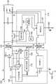
图1是根据本公开的一方面的具有混合次级侧调节的改进的反激转换器的电路图。1 is a circuit diagram of an improved flyback converter with hybrid secondary side regulation in accordance with an aspect of the present disclosure.
图2示出了在检测变压器复位时间期间的辅助绕组电压波形。Figure 2 shows the auxiliary winding voltage waveform during the reset time of the detection transformer.
通过参考接下来的具体实施方式,本公开的实施例及其优点得到最好的理解。应当认识到,相似的附图标记用于标识一个或多个附图中所示的相似元素。Embodiments of the present disclosure and their advantages are best understood by reference to the detailed description which follows. It should be appreciated that like reference numerals are used to identify like elements shown in one or more of the figures.
具体实施方式Detailed ways
现在转到附图,图1中示出了示例反激转换器100。初级侧控制器105包括用于控制NMOS功率开关晶体管M1的循环的开关控制器111。在替代实施例中,可以使用其他类型的功率开关晶体管,诸如GaN功率开关晶体管或双极结型功率开关晶体管。当功率开关晶体管M1被循环接通时,取决于输入电压轨(rail)上的输入电压Vin和初级绕组T1的磁化电感,磁化电流开始流过变压器101的初级绕组T1。如在反激转换器领域中已知的,开关控制器111可以在低到中等负载水平期间使用谷值模式开关来循环功率开关晶体管M1。然而,在高功率操作模式期间,使用零电压开关来循环功率开关晶体管M1是更有利的。Turning now to the drawings, an
为了实现零电压开关,功率开关晶体管M1的漏极连接到NMOS高边(HS)开关晶体管的源极,HS开关晶体管具有通过电容器C连接到输入电压轨的漏极。为了实现零电压开关,在功率开关晶体管M1已被循环关断之后,开关控制器111可以使HS开关晶体管循环接通。然后将绕组T1的漏电感(leakage inductance)能量存储在电容器C1上。当HS开关晶体管被循环关断时,功率开关晶体管M1的漏极将被拉至地(ground)。为了检测该漏极电压的过零点,开关控制器111可包括过零检测器,诸如比较器155,其将漏极电压与地进行比较。当比较器155指示漏极电压被放电时,开关控制器111然后可以在随后的开关循环中使功率开关晶体管M1循环接通,其中功率开关晶体管M1的漏极到源极电压为零,如在零电压开关领域中已知的。To achieve zero voltage switching, the drain of power switch transistor M1 is connected to the source of an NMOS high-side (HS) switching transistor, which has a drain connected through capacitor C to the input voltage rail. To achieve zero voltage switching, the
当功率开关晶体管M1导通时,变压器101的次级绕组S1不传导。例如,次级侧控制器111可包括同步整流(SR)控制器135,其监视NMOS SR开关晶体管的漏极到源极电压。当SR开关晶体管的漏极到源极电压指示电源开关M1被关闭时,SR控制器135使SR开关晶体管循环接通。如本文将进一步解释的,SR开关晶体管的导通控制还可以响应于来自初级侧控制器105的通信——即功率开关晶体管M1已被循环关断。以这种方式,避免了穿通的危险,其中在功率开关晶体管M1仍然导通时SR开关晶体管被循环接通。SR控制器135还可以监视SR开关晶体管的源极到漏极电压,以确定何时使SR开关晶体管循环关断。When the power switch transistor M1 is turned on, the secondary winding S1 of the
有利地,仅在稳态操作期间实施输出电压的次级侧调节。如本文将进一步解释的,仅初级反馈信息由初级侧控制器105用于在转变到稳态操作之前控制平滑启动模式。为了在稳态操作期间执行输出电压的次级侧调节,次级侧控制器110包括误差放大器140,其响应于反激转换器的输出电压VBUS与参考电压(诸如来自带隙(bandgap,BG)源145的带隙电压)之间的差异而生成误差电压Verr。注意,在替代实施例中,这两个电压的缩放版本可以应用于误差放大器140。环路滤波器145对误差电压进行滤波以产生控制电压Vc。然后该控制电压可被传送到初级侧控制器105,如本文进一步讨论的。Advantageously, secondary-side regulation of the output voltage is only implemented during steady state operation. As will be explained further herein, only the primary feedback information is used by the
在SR开关晶体管导通时流动的次级绕组电流利用输出电压VBUS对输出电容器Cout充电。该输出电压通过如在数据电缆接口领域中已知的诸如USB电缆接口130之类的数据电缆接口对负载(未示出)充电,USB电缆接口130还包括D+端子、D-端子和接地端子。通信接口150监视数据端子D+和D-以检测移动设备是否已被连接到数据电缆接口。如果检测到移动设备,则次级侧控制器110可以通过隔离通信信道(诸如具有次级绕组S2和初级绕组T3的信号变压器170)警告初级侧控制器105。替代的隔离通信信道包括诸如通过光电二极管160和接收双极结型晶体管165形成的光隔离器。或者,电容器(未示出)也可用于形成合适的隔离通信信道。有利地,信号变压器170是双向的,使得它支持从次级侧控制器110到初级侧控制器105以及从初级侧控制器105到次级侧控制器110的通信。The secondary winding current flowing when the SR switching transistor is on charges the output capacitor Cout with the output voltage VBUS. This output voltage charges a load (not shown) through a data cable interface such as
通信接口150通过次级绕组S2使用数字或模拟的信令来发送控制电压,以在初级绕组T3上引起由通信接口125接收的对应的数字或模拟的信号。在替代实施例中,可以发送误差电压,使得初级侧控制器105将执行环路滤波。通信接口125然后可以将控制电压(或误差电压)恢复为数字或模拟的信号,使得其可以由开关控制器111处理。开关控制器111然后可以将控制电压处理成如在脉冲频率调制中使用的脉冲开关频率,或将控制电压处理成脉冲宽度调制的峰值开关电流,如在反激领域中已知的。无论根据脉冲频率调制还是根据脉冲宽度调制来循环功率开关晶体管M1,开关控制器111都将相应地使功率开关晶体管M1循环接通和循环关断。例如,在脉冲宽度调制操作模式中,开关控制器响应于对控制电压的处理而确定功率开关晶体管M1的电流开关周期的峰值电流。该处理可以包括使用如在反激领域中已知的比例—积分(PI)或比例—积分—微分(PID)控制。在功率开关晶体管M1的导通时间期间,开关控制器111通过感测电阻器Rs来监视由功率开关晶体管M1传导的漏极电流ID,感测电阻器Rs耦合在功率开关晶体管M1的源极和地之间。感测电阻器两端产生的电流感测(CS)电压表示漏极电流。当开关控制器111检测到漏极电流(如通过CS电压所感测的)等于期望的峰值电流时,它使功率开关晶体管M1循环关断。
基于对控制电压的处理所产生的功率开关晶体管M1的循环导致输出电压VBUS的恒定电压操作模式。但是如先前讨论,存在多种操作模式,诸如对已放电电池充电的初始阶段,其中恒定电压操作将导致流入电池的过高水平的输出电流。为了防止发生这样潜在危险水平的输出电流,初级侧控制器105使用仅初级反馈技术来检测变压器复位时间。由于初级绕组电流的峰值是已知的,因此次级绕组电流的峰值也是已知的,因为它通过变压器101的匝数比而与峰值绕组电流成比例。因此,初级侧控制器105可以有利地使用变压器复位时间来基于开关周期、峰值次级绕组电流和变压器复位时间计算平均输出电流。如果该平均输出电流超过电流限制,则开关控制器111然后可以在下一个开关周期中“忽略”控制电压,并且改为控制功率开关晶体管M1的导通时间来产生如通过仅初级反馈技术所监视的期望峰值电流。The cycling of the power switch transistor M1 based on the processing of the control voltage results in a constant voltage mode of operation of the output voltage VBUS. But as previously discussed, there are various modes of operation, such as the initial phase of charging a discharged battery, where constant voltage operation would result in an excessively high level of output current flowing into the battery. To prevent such potentially dangerous levels of output current from occurring, the primary-
作为结果的混合控制是相当有利的,因为反激转换器100然后享有如通过次级侧调节实现的准确恒定电压操作,而没有变压器101的次级侧的感测电阻器的电力抢夺需求。为了检测变压器复位时间,初级侧控制器105可以通过分压器120感测辅助绕组T2上的辅助绕组电压。然后由波形分析器处理所产生的分压后的辅助绕组电压,以检测辅助绕组电压中的“拐点(knee)”。这可以参考图2得到更好地理解,图2示出了响应于在时间t0使电源开关循环关闭的辅助绕组电压VAUX。作为响应,辅助绕组电压将跳高。在某一吉布斯(Gibbs)振荡之后,辅助绕组电压然后将随着次级电流(未示出)斜坡变为零而缓慢斜坡下降。当次级电流耗尽时,辅助绕组电压在时间t1达到其拐点,于是它迅速下降并开始共振振荡。时间t0和t1之间的持续时间是变压器复位时间(TRST)。The resulting hybrid control is quite advantageous because the
在仅初级反馈中,通过图2所示的方程1的反演来检测输出电压Vo将是常规的。但是次级侧调节已经准确得多地提供了该输出电压。因此,初级侧控制器101所需要的是变压器复位时间本身,从而可以确定输出电流。如在仅初级反馈技术中已知的,存在多种检测拐点(以及因此变压器复位时间)以及其他波形形状和定时信息(诸如拐点电压,波形的持续时间,共振振铃周期,以及谷值和峰值检测)的方式,使得波形分析器115的细节将被本领域普通技术人员理解。无论初级侧控制器如何检测变压器复位时间,开关控制器111然后可以继续相应地计算输出电流。In primary-only feedback, it would be conventional to detect the output voltage Vo by the inversion of Equation 1 shown in Figure 2. But secondary side regulation already provides this output voltage much more accurately. Therefore, all that is required by the
但是请注意,Vsense波形本身还可以被初级侧控制器105用于除了仅检测变压器复位时间之外的目的。例如,初级侧控制器105可以使用拐点电压以及电流感测电压来确保在启动期间输出电压的平滑过渡。例如,当反激转换器100从零或非常低的输出电压启动时,输出电压调节远离其稳定状态,所以难以具有输出电压的平滑增加。通过智能地处理和利用初级侧中的Vsense和电流感测信息,反激转换器100可以实现平滑启动,而没有过冲(overshoot)、下冲(undershoot)、振荡或其他不期望的行为。一旦启动完成并且电压稳定到接近参考点,初级侧控制就可以决定切换到次级侧调节,这将在稳态下实现更精确的电压调节。此外,波形分析器115可被配置用于谷值检测,使得开关控制器111可以根据谷值模式切换来接通功率开关晶体管M1。还请注意,监视Vsense波形的能力使初级侧控制器105能够检测异常状况或故障状况,诸如辅助绕组开路、短路或软短路。特别是,如果辅助绕组T2由于例如电路板故障而接地,则Vsense波形将保持在零伏特。波形分析器115然后可以检测到Vsense波形的该不足,使得开关控制器111可以停止功率开关晶体管M1的循环。辅助绕组T3的开路也将引起异常Vsense波形,该异常Vsense波形可被波形分析器115检测到,使得开关控制器115可以停止功率开关晶体管M1的循环。其他故障示例可包括电流感测(CS)电阻器短路(或部分短路)、CS电阻器开路以及控制器引脚短路或开路。通过在初级侧智能地处理和利用这些指示,初级侧控制器可以检测异常和故障,并进行快速适当动作(诸如关闭电源开关),而无需等待次级侧进行检测和发送警报(这将太晚)。Note, however, that the Vsense waveform itself can also be used by the
本领域普通技术人员还将认识到,可以针对反激转换器100进行许多修改。例如,初级侧控制器105可以向次级侧控制器110警告HS和M1电源开关的接通/关闭状态。以这种方式,可以避免穿通的危险以及错误的零电压切换。此外,变压器复位时间的检测使开关控制器110能够检测辅助绕组T3处的短路或开路,从而可以相应地警告次级侧控制器110。此外,变压器复位时间以及其他波形形状和定时信息的检测使开关控制器111能够检测过压或欠压状况,从而可以相应地警告初级侧控制器105。总之,反激转换器将保留仅初级反馈技术、特性和能力,同时利用次级侧调节进行稳态电压调节,并且它还将具有初级侧和次级侧之间的双向通信。因此,本领域技术人员将认识到,在不脱离本公开的范围的情况下,可以在本公开的设备的材料、装置、配置和使用方法中进行许多修改、替换和变化并可以对本公开的设备的材料、装置、配置和使用方法进行许多修改、替换和变化。鉴于此,本公开的范围不应限于本文示出和描述的特定实施例的范围,因为它们仅仅当作其一些示例,而是应该与所附权利要求及其功能等同物的范围完全相称。Those of ordinary skill in the art will also recognize that many modifications may be made to the
Claims (9)
Applications Claiming Priority (3)
| Application Number | Priority Date | Filing Date | Title |
|---|---|---|---|
| US201762445660P | 2017-01-12 | 2017-01-12 | |
| US62/445,660 | 2017-01-12 | ||
| PCT/US2018/013655WO2018132761A1 (en) | 2017-01-12 | 2018-01-12 | Hybrid secondary-side regulation |
Publications (2)
| Publication Number | Publication Date |
|---|---|
| CN110073584A CN110073584A (en) | 2019-07-30 |
| CN110073584Btrue CN110073584B (en) | 2022-06-14 |
Family
ID=62840402
Family Applications (1)
| Application Number | Title | Priority Date | Filing Date |
|---|---|---|---|
| CN201880004926.4AActiveCN110073584B (en) | 2017-01-12 | 2018-01-12 | Hybrid secondary side regulation |
Country Status (3)
| Country | Link |
|---|---|
| US (4) | US10461646B2 (en) |
| CN (1) | CN110073584B (en) |
| WO (1) | WO2018132761A1 (en) |
Families Citing this family (31)
| Publication number | Priority date | Publication date | Assignee | Title |
|---|---|---|---|---|
| US10320301B2 (en) | 2017-09-15 | 2019-06-11 | Semiconductor Components Industries, Llc | Power converter responsive to device connection status |
| DE102017126696A1 (en)* | 2017-11-14 | 2019-05-16 | Infineon Technologies Austria Ag | Voltage transformer control, voltage converter and method of operating a voltage converter |
| CN109995254B (en)* | 2017-12-29 | 2020-12-29 | 东南大学 | A method for improving dynamic performance of synchronous rectifier primary-side feedback flyback power supply |
| DE102018116883A1 (en)* | 2018-07-12 | 2020-01-16 | Infineon Technologies Austria Ag | Flyback converter control, flyback converter and method for operating the flyback converter |
| US10367422B1 (en)* | 2018-10-26 | 2019-07-30 | Infineon Technologies Austria Ag | Valley mode switching with fixed frequency for switching mode power supply |
| TWI681615B (en) | 2018-10-31 | 2020-01-01 | 通嘉科技股份有限公司 | Secondary controller applied to a secondary side of a power converter and operation method thereof |
| JP7168422B2 (en)* | 2018-11-22 | 2022-11-09 | ローム株式会社 | Isolated DC/DC converters, AC/DC converters, power adapters and electrical equipment |
| US10763756B2 (en) | 2018-12-13 | 2020-09-01 | Power Integrations, Inc. | Apparatus and methods for sensing resonant circuit signals to enhance control in a resonant converter |
| US10693384B1 (en)* | 2019-06-26 | 2020-06-23 | Cypress Semiconductor Corporation | Accurate feed-forward sensing in flyback-transformer based secondary controller |
| US10651753B1 (en) | 2019-06-26 | 2020-05-12 | Cypress Semiconductor Corporation | Accurate valley detection for secondary controlled flyback converter |
| US10554140B1 (en) | 2019-06-26 | 2020-02-04 | Cypress Semiconductor Corporation | AC-DC converter with secondary side-control and synchronous rectifier sense architecture |
| US10651754B1 (en) | 2019-06-26 | 2020-05-12 | Cypress Semiconductor Corporation | Accurate peak detection architecture for secondary controlled AC-DC converter |
| US11758631B2 (en) | 2019-06-27 | 2023-09-12 | Tridonic Gmbh & Co Kg | Synchronous flyback converter for driving LED loads |
| US10951107B2 (en)* | 2019-06-27 | 2021-03-16 | Cypress Semiconductor Corporation | Communicating fault indications between primary and secondary controllers in a secondary-controlled flyback converter |
| US10756644B1 (en)* | 2019-08-22 | 2020-08-25 | Cypress Semiconductor Corporation | Controlled gate-source voltage N-channel field effect transistor (NFET) gate driver |
| CN110611431B (en)* | 2019-09-30 | 2020-06-23 | 东南大学 | Primary side regulation control system and control method of active clamp flyback converter |
| US11223283B2 (en)* | 2020-04-20 | 2022-01-11 | Dialog Semiconductor Inc. | Universal output current regulation for a flyback converter |
| TWI736275B (en)* | 2020-05-21 | 2021-08-11 | 宏碁股份有限公司 | Power supply device for over current protection |
| US11394303B2 (en)* | 2020-05-29 | 2022-07-19 | Dialog Semiconductor, Inc. | Flyback converter with synchronous rectifier switch fault detection |
| US11736026B2 (en)* | 2020-05-29 | 2023-08-22 | Dialog Semiconductor Inc. | Flyback converter with fast load transient detection |
| US11527962B2 (en)* | 2020-09-14 | 2022-12-13 | Dialog Semiconductor Inc. | Power adapter having ultra low standby power |
| CN112467992A (en)* | 2020-11-30 | 2021-03-09 | 北京精密机电控制设备研究所 | Magnetic isolation feedback power conversion circuit |
| US12155313B2 (en)* | 2021-02-10 | 2024-11-26 | Innoscience (Suzhou) Technology Co., Ltd. | Multi-functional PCB for assembling GaN-based power converter |
| US11916490B2 (en) | 2021-02-10 | 2024-02-27 | Innoscience (Suzhou) Technology Co., Ltd. | Multi-functional PCB for assembling GaN-based power converter |
| US11916488B2 (en)* | 2021-02-10 | 2024-02-27 | Innoscience (Suzhou) Technology Co., Ltd. | High efficiency and high density GaN-based power converter |
| US11916489B2 (en) | 2021-02-10 | 2024-02-27 | Innoscience (Suzhou) Technology Co., Ltd. | High efficiency and high density GaN-based power converter |
| WO2022170577A1 (en) | 2021-02-10 | 2022-08-18 | Innoscience (Suzhou) Technology Co., Ltd. | HIGH EFFICIENCY AND HIGH DENSITY GaN- BASED POWER CONVERTER AND METHOD FOR MANUFACTURING THE SAME |
| US11916005B2 (en) | 2021-02-10 | 2024-02-27 | Innoscience (Suzhou) Technology Co., Ltd. | Multi-functional PCB for assembling GaN-based power converter and method for manufacturing the same |
| CN115800747B (en)* | 2021-09-10 | 2025-07-04 | 台达电子企业管理(上海)有限公司 | Hybrid flyback circuit and control method |
| TWI858945B (en)* | 2023-10-03 | 2024-10-11 | 群光電能科技股份有限公司 | Power converter and method for feedback control the same |
| WO2025136361A1 (en)* | 2023-12-19 | 2025-06-26 | Power Integrations, Inc. | Magnetic assembly with an integrated communication link |
Citations (4)
| Publication number | Priority date | Publication date | Assignee | Title |
|---|---|---|---|---|
| CN103227568A (en)* | 2012-01-26 | 2013-07-31 | 凌力尔特公司 | Flyback converter with primary side voltage sensing and overvoltage protection during low load operation |
| CN103296904A (en)* | 2012-02-29 | 2013-09-11 | 黄煜梅 | Power-factor correction constant current controller and control method |
| CN103840673A (en)* | 2012-11-20 | 2014-06-04 | 德克萨斯仪器股份有限公司 | Flyback power supply regulation apparatus and methods |
| CN104052290A (en)* | 2013-03-13 | 2014-09-17 | 戴乐格半导体公司 | Switching Power Converter with Secondary-to-Primary Messaging |
Family Cites Families (32)
| Publication number | Priority date | Publication date | Assignee | Title |
|---|---|---|---|---|
| EP1495531B1 (en)* | 2002-04-12 | 2006-05-17 | DET International Holding Limited | High efficiency flyback converter |
| US7443700B2 (en)* | 2006-11-09 | 2008-10-28 | Iwatt Inc. | On-time control for constant current mode in a flyback power supply |
| US7911808B2 (en)* | 2007-02-10 | 2011-03-22 | Active-Semi, Inc. | Primary side constant output current controller with highly improved accuracy |
| US7974109B2 (en)* | 2007-05-07 | 2011-07-05 | Iwatt Inc. | Digital compensation for cable drop in a primary side control power supply controller |
| US8553431B2 (en)* | 2009-02-03 | 2013-10-08 | Iwatt Inc. | Switching power converter with load impedance detection |
| US8199537B2 (en)* | 2009-02-19 | 2012-06-12 | Iwatt Inc. | Detecting light load conditions and improving light load efficiency in a switching power converter |
| TWI431918B (en)* | 2009-06-19 | 2014-03-21 | Leadtrend Tech Corp | Control method, constant current control method, method for generating a real current source to represent average current through a winding, constant current and constant voltage power converter, switch controller, and average voltage detector |
| TW201123701A (en)* | 2009-12-23 | 2011-07-01 | Leadtrend Tech Corp | Control method and controller |
| JP5223874B2 (en)* | 2010-03-09 | 2013-06-26 | 株式会社村田製作所 | Isolated switching power supply |
| JP5170165B2 (en)* | 2010-06-11 | 2013-03-27 | 株式会社村田製作所 | Isolated switching power supply |
| TWI477051B (en)* | 2011-03-28 | 2015-03-11 | Neoenergy Microelectronics Inc | Flyback converter with primary side and secondary side control and method for the same |
| KR101858059B1 (en)* | 2011-08-17 | 2018-06-29 | 페어차일드코리아반도체 주식회사 | Switch control circuit, power factor corrector comprising the same, and driving mehtod of the power factor corrector |
| TWI496396B (en)* | 2012-02-18 | 2015-08-11 | Richtek Technology Corp | Isolated power converter circuit and control circuit and control method thereof |
| US8780590B2 (en)* | 2012-05-03 | 2014-07-15 | Hong Kong Applied Science & Technology Research Institute Company, Ltd. | Output current estimation for an isolated flyback converter with variable switching frequency control and duty cycle adjustment for both PWM and PFM modes |
| US9071152B2 (en) | 2012-07-03 | 2015-06-30 | Cognipower, Llc | Power converter with demand pulse isolation |
| US9331589B2 (en)* | 2012-09-24 | 2016-05-03 | Dialog Semiconductor Inc. | Primary feedback switching power converter controller with intelligent determination of and response to output voltage drops due to dynamic load conditions |
| EP2717450B1 (en)* | 2012-10-05 | 2016-12-28 | Nxp B.V. | Isolated switched-mode power supply |
| JP2014166024A (en)* | 2013-02-25 | 2014-09-08 | Rohm Co Ltd | Power supply device and startup method for the same, ac adapter, electronic apparatus, and power supply system |
| KR20150025935A (en)* | 2013-08-30 | 2015-03-11 | 삼성전기주식회사 | Circuit for generating reference signal for controlling peak current of converter switch, isolated converter and method for generating reference signal for controlling peak current of converter switch |
| TWI560537B (en)* | 2013-10-04 | 2016-12-01 | Leadtrend Tech Corp | Controller for adjusting an output voltage of a power converter |
| US9379625B2 (en)* | 2013-12-26 | 2016-06-28 | Dialog Semiconductor Inc. | Current meter for load modulation communication receiver architecture |
| US9825541B2 (en)* | 2014-01-17 | 2017-11-21 | Fairchild Korea Semiconductor Ltd. | Output current estimating method and power supply device using the same |
| CN103944427B (en)* | 2014-05-09 | 2016-02-03 | 东南大学 | A kind of control method of AC-DC converter output current and control system thereof |
| CN105305825B (en)* | 2014-07-18 | 2018-02-09 | 绿达光电股份有限公司 | power supply controller and related control method |
| US9742288B2 (en) | 2014-10-21 | 2017-08-22 | Power Integrations, Inc. | Output-side controller with switching request at relaxation ring extremum |
| US9819274B2 (en)* | 2014-11-20 | 2017-11-14 | Microchip Technology Incorporated | Start-up controller for a power converter |
| CN104660022B (en)* | 2015-02-02 | 2017-06-13 | 昂宝电子(上海)有限公司 | The system and method that overcurrent protection is provided for supply convertor |
| CN104767372B (en)* | 2015-04-24 | 2017-12-19 | 矽力杰半导体技术(杭州)有限公司 | Control circuit, control method and apply its inverse excitation type converter |
| US9774270B2 (en)* | 2015-06-15 | 2017-09-26 | Apple Inc. | Systems and methods of operation for power converters having series-parallel mode active clamps |
| US10868473B2 (en)* | 2015-11-30 | 2020-12-15 | Semiconductor Components Industries, Llc | Secondary side controlled control circuit for power converter with synchronous rectifier |
| JP2017163779A (en)* | 2016-03-11 | 2017-09-14 | ローム株式会社 | Power supply device, primary side controller, ac adapter, electronic equipment, and short-circuit detection method |
| US9973094B2 (en)* | 2016-03-31 | 2018-05-15 | Infineon Technologies Austria Ag | Power converter and power conversion method |
- 2018
- 2018-01-12CNCN201880004926.4Apatent/CN110073584B/enactiveActive
- 2018-01-12WOPCT/US2018/013655patent/WO2018132761A1/ennot_activeCeased
- 2018-08-10USUS16/100,934patent/US10461646B2/enactiveActive
- 2019
- 2019-09-30USUS16/588,854patent/US10855188B2/enactiveActive
- 2020
- 2020-12-01USUS17/109,006patent/US20210083586A1/ennot_activeAbandoned
- 2022
- 2022-01-18USUS17/578,353patent/US11955895B2/enactiveActive
Patent Citations (4)
| Publication number | Priority date | Publication date | Assignee | Title |
|---|---|---|---|---|
| CN103227568A (en)* | 2012-01-26 | 2013-07-31 | 凌力尔特公司 | Flyback converter with primary side voltage sensing and overvoltage protection during low load operation |
| CN103296904A (en)* | 2012-02-29 | 2013-09-11 | 黄煜梅 | Power-factor correction constant current controller and control method |
| CN103840673A (en)* | 2012-11-20 | 2014-06-04 | 德克萨斯仪器股份有限公司 | Flyback power supply regulation apparatus and methods |
| CN104052290A (en)* | 2013-03-13 | 2014-09-17 | 戴乐格半导体公司 | Switching Power Converter with Secondary-to-Primary Messaging |
Also Published As
| Publication number | Publication date |
|---|---|
| US20180351462A1 (en) | 2018-12-06 |
| US11955895B2 (en) | 2024-04-09 |
| CN110073584A (en) | 2019-07-30 |
| US10855188B2 (en) | 2020-12-01 |
| US20210083586A1 (en) | 2021-03-18 |
| US20200036291A1 (en) | 2020-01-30 |
| US20220140735A1 (en) | 2022-05-05 |
| US10461646B2 (en) | 2019-10-29 |
| WO2018132761A1 (en) | 2018-07-19 |
Similar Documents
| Publication | Publication Date | Title |
|---|---|---|
| CN110073584B (en) | Hybrid secondary side regulation | |
| US11201556B2 (en) | Accurate peak detection architecture for secondary controlled AC-DC converter | |
| US10903752B2 (en) | AC-DC converter with secondary side-control and synchronous rectifier sense architecture | |
| US10651753B1 (en) | Accurate valley detection for secondary controlled flyback converter | |
| US9407155B2 (en) | Isolated switching converter with secondary side modulation and control method | |
| US9331589B2 (en) | Primary feedback switching power converter controller with intelligent determination of and response to output voltage drops due to dynamic load conditions | |
| US9866108B2 (en) | PFC shutdown circuit for light load | |
| US8976547B2 (en) | Switching mode power supply with synchronous rectifying control circuit | |
| US7633780B2 (en) | Switching power supply apparatus with low loss synchronous rectification | |
| US8693217B2 (en) | Power supply controller with minimum-sum multi-cycle modulation | |
| CN103904903B (en) | Flyback converter | |
| CN110879319B (en) | Voltage and current protection using secondary side rectified voltage sensing | |
| US9647560B2 (en) | Secondary-side dynamic load detection and communication device | |
| TW201334377A (en) | Isolated flyback converter with efficient light load operation | |
| US20150280573A1 (en) | System and Method for a Switched-Mode Power Supply | |
| JP4950320B2 (en) | Switching power supply | |
| JP2007014196A (en) | Method for detecting failure in switching power supply and detecting apparatus thereof | |
| WO2012077588A1 (en) | Insulating direct current power supply device | |
| US10483861B1 (en) | Flyback converter controller with single pin detection of over-voltage and auxiliary winding faults | |
| CN118432449A (en) | Controller for power converter, power converter and operation method thereof | |
| US12308758B2 (en) | Switching mode power supply with stable zero crossing detection, the control circuit and the method thereof | |
| US12155312B2 (en) | Power converter controller, power converter and method for operating control of a power stage based on an intermediate voltage with respect to a threshold value determined from a turns ratio of a transformer | |
| US12074528B2 (en) | Secondary side controlled QR flyback converter using a programmable valley algorithm | |
| US10742125B1 (en) | Direct feedback for isolated switching converters | |
| Mode | Integrated Critical Mode PFC/Quasi-Resonant Current Mode PWM Controller |
Legal Events
| Date | Code | Title | Description |
|---|---|---|---|
| PB01 | Publication | ||
| PB01 | Publication | ||
| SE01 | Entry into force of request for substantive examination | ||
| SE01 | Entry into force of request for substantive examination | ||
| GR01 | Patent grant | ||
| GR01 | Patent grant |